EP3385982A1 - Halbleiterchip, halbleiterbauelement und elektronische vorrichtung - Google Patents
Halbleiterchip, halbleiterbauelement und elektronische vorrichtung Download PDFInfo
- Publication number
- EP3385982A1 EP3385982A1 EP15909815.1A EP15909815A EP3385982A1 EP 3385982 A1 EP3385982 A1 EP 3385982A1 EP 15909815 A EP15909815 A EP 15909815A EP 3385982 A1 EP3385982 A1 EP 3385982A1
- Authority
- EP
- European Patent Office
- Prior art keywords
- semiconductor
- power transistor
- surface electrode
- semiconductor chip
- back surface
- Prior art date
- Legal status (The legal status is an assumption and is not a legal conclusion. Google has not performed a legal analysis and makes no representation as to the accuracy of the status listed.)
- Withdrawn
Links
Images


Classifications
-
- H—ELECTRICITY
- H10—SEMICONDUCTOR DEVICES; ELECTRIC SOLID-STATE DEVICES NOT OTHERWISE PROVIDED FOR
- H10D—INORGANIC ELECTRIC SEMICONDUCTOR DEVICES
- H10D84/00—Integrated devices formed in or on semiconductor substrates that comprise only semiconducting layers, e.g. on Si wafers or on GaAs-on-Si wafers
- H10D84/01—Manufacture or treatment
- H10D84/0123—Integrating together multiple components covered by H10D12/00 or H10D30/00, e.g. integrating multiple IGBTs
- H10D84/0126—Integrating together multiple components covered by H10D12/00 or H10D30/00, e.g. integrating multiple IGBTs the components including insulated gates, e.g. IGFETs
- H10D84/016—Integrating together multiple components covered by H10D12/00 or H10D30/00, e.g. integrating multiple IGBTs the components including insulated gates, e.g. IGFETs the components including vertical IGFETs
-
- H—ELECTRICITY
- H01—ELECTRIC ELEMENTS
- H01M—PROCESSES OR MEANS, e.g. BATTERIES, FOR THE DIRECT CONVERSION OF CHEMICAL ENERGY INTO ELECTRICAL ENERGY
- H01M10/00—Secondary cells; Manufacture thereof
- H01M10/42—Methods or arrangements for servicing or maintenance of secondary cells or secondary half-cells
- H01M10/44—Methods for charging or discharging
-
- H—ELECTRICITY
- H02—GENERATION; CONVERSION OR DISTRIBUTION OF ELECTRIC POWER
- H02J—ELECTRIC POWER NETWORKS; CIRCUIT ARRANGEMENTS OR SYSTEMS FOR SUPPLYING OR DISTRIBUTING ELECTRIC POWER; SYSTEMS FOR STORING ELECTRIC ENERGY
- H02J7/00—Circuit arrangements for charging or discharging batteries or for supplying loads from batteries
- H02J7/60—Circuit arrangements for charging or discharging batteries or for supplying loads from batteries including safety or protection arrangements
- H02J7/663—Circuit arrangements for charging or discharging batteries or for supplying loads from batteries including safety or protection arrangements using battery or load disconnect circuits
-
- H—ELECTRICITY
- H02—GENERATION; CONVERSION OR DISTRIBUTION OF ELECTRIC POWER
- H02J—ELECTRIC POWER NETWORKS; CIRCUIT ARRANGEMENTS OR SYSTEMS FOR SUPPLYING OR DISTRIBUTING ELECTRIC POWER; SYSTEMS FOR STORING ELECTRIC ENERGY
- H02J7/00—Circuit arrangements for charging or discharging batteries or for supplying loads from batteries
- H02J7/90—Regulation of charging or discharging current or voltage
- H02J7/92—Regulation of charging or discharging current or voltage with prioritisation of loads or sources
-
- H—ELECTRICITY
- H03—ELECTRONIC CIRCUITRY
- H03K—PULSE TECHNIQUE
- H03K17/00—Electronic switching or gating, i.e. not by contact-making and –breaking
- H03K17/51—Electronic switching or gating, i.e. not by contact-making and –breaking characterised by the components used
- H03K17/56—Electronic switching or gating, i.e. not by contact-making and –breaking characterised by the components used by the use, as active elements, of semiconductor devices
- H03K17/687—Electronic switching or gating, i.e. not by contact-making and –breaking characterised by the components used by the use, as active elements, of semiconductor devices the devices being field-effect transistors
- H03K17/6871—Electronic switching or gating, i.e. not by contact-making and –breaking characterised by the components used by the use, as active elements, of semiconductor devices the devices being field-effect transistors the output circuit comprising more than one controlled field-effect transistor
- H03K17/6874—Electronic switching or gating, i.e. not by contact-making and –breaking characterised by the components used by the use, as active elements, of semiconductor devices the devices being field-effect transistors the output circuit comprising more than one controlled field-effect transistor in a symmetrical configuration
-
- H—ELECTRICITY
- H10—SEMICONDUCTOR DEVICES; ELECTRIC SOLID-STATE DEVICES NOT OTHERWISE PROVIDED FOR
- H10D—INORGANIC ELECTRIC SEMICONDUCTOR DEVICES
- H10D30/00—Field-effect transistors [FET]
- H10D30/60—Insulated-gate field-effect transistors [IGFET]
- H10D30/64—Double-diffused metal-oxide semiconductor [DMOS] FETs
- H10D30/66—Vertical DMOS [VDMOS] FETs
- H10D30/668—Vertical DMOS [VDMOS] FETs having trench gate electrodes, e.g. UMOS transistors
-
- H—ELECTRICITY
- H10—SEMICONDUCTOR DEVICES; ELECTRIC SOLID-STATE DEVICES NOT OTHERWISE PROVIDED FOR
- H10D—INORGANIC ELECTRIC SEMICONDUCTOR DEVICES
- H10D84/00—Integrated devices formed in or on semiconductor substrates that comprise only semiconducting layers, e.g. on Si wafers or on GaAs-on-Si wafers
- H10D84/01—Manufacture or treatment
- H10D84/02—Manufacture or treatment characterised by using material-based technologies
- H10D84/03—Manufacture or treatment characterised by using material-based technologies using Group IV technology, e.g. silicon technology or silicon-carbide [SiC] technology
- H10D84/038—Manufacture or treatment characterised by using material-based technologies using Group IV technology, e.g. silicon technology or silicon-carbide [SiC] technology using silicon technology, e.g. SiGe
-
- H—ELECTRICITY
- H10—SEMICONDUCTOR DEVICES; ELECTRIC SOLID-STATE DEVICES NOT OTHERWISE PROVIDED FOR
- H10D—INORGANIC ELECTRIC SEMICONDUCTOR DEVICES
- H10D84/00—Integrated devices formed in or on semiconductor substrates that comprise only semiconducting layers, e.g. on Si wafers or on GaAs-on-Si wafers
- H10D84/80—Integrated devices formed in or on semiconductor substrates that comprise only semiconducting layers, e.g. on Si wafers or on GaAs-on-Si wafers characterised by the integration of at least one component covered by groups H10D12/00 or H10D30/00, e.g. integration of IGFETs
- H10D84/82—Integrated devices formed in or on semiconductor substrates that comprise only semiconducting layers, e.g. on Si wafers or on GaAs-on-Si wafers characterised by the integration of at least one component covered by groups H10D12/00 or H10D30/00, e.g. integration of IGFETs of only field-effect components
- H10D84/83—Integrated devices formed in or on semiconductor substrates that comprise only semiconducting layers, e.g. on Si wafers or on GaAs-on-Si wafers characterised by the integration of at least one component covered by groups H10D12/00 or H10D30/00, e.g. integration of IGFETs of only field-effect components of only insulated-gate FETs [IGFET]
- H10D84/83125—Integrated devices formed in or on semiconductor substrates that comprise only semiconducting layers, e.g. on Si wafers or on GaAs-on-Si wafers characterised by the integration of at least one component covered by groups H10D12/00 or H10D30/00, e.g. integration of IGFETs of only field-effect components of only insulated-gate FETs [IGFET] the IGFETs characterised by having shared source or drain regions
-
- H—ELECTRICITY
- H10—SEMICONDUCTOR DEVICES; ELECTRIC SOLID-STATE DEVICES NOT OTHERWISE PROVIDED FOR
- H10D—INORGANIC ELECTRIC SEMICONDUCTOR DEVICES
- H10D84/00—Integrated devices formed in or on semiconductor substrates that comprise only semiconducting layers, e.g. on Si wafers or on GaAs-on-Si wafers
- H10D84/80—Integrated devices formed in or on semiconductor substrates that comprise only semiconducting layers, e.g. on Si wafers or on GaAs-on-Si wafers characterised by the integration of at least one component covered by groups H10D12/00 or H10D30/00, e.g. integration of IGFETs
- H10D84/82—Integrated devices formed in or on semiconductor substrates that comprise only semiconducting layers, e.g. on Si wafers or on GaAs-on-Si wafers characterised by the integration of at least one component covered by groups H10D12/00 or H10D30/00, e.g. integration of IGFETs of only field-effect components
- H10D84/83—Integrated devices formed in or on semiconductor substrates that comprise only semiconducting layers, e.g. on Si wafers or on GaAs-on-Si wafers characterised by the integration of at least one component covered by groups H10D12/00 or H10D30/00, e.g. integration of IGFETs of only field-effect components of only insulated-gate FETs [IGFET]
- H10D84/837—Integrated devices formed in or on semiconductor substrates that comprise only semiconducting layers, e.g. on Si wafers or on GaAs-on-Si wafers characterised by the integration of at least one component covered by groups H10D12/00 or H10D30/00, e.g. integration of IGFETs of only field-effect components of only insulated-gate FETs [IGFET] comprising vertical IGFETs
- H10D84/839—Integrated devices formed in or on semiconductor substrates that comprise only semiconducting layers, e.g. on Si wafers or on GaAs-on-Si wafers characterised by the integration of at least one component covered by groups H10D12/00 or H10D30/00, e.g. integration of IGFETs of only field-effect components of only insulated-gate FETs [IGFET] comprising vertical IGFETs comprising VDMOS
-
- H—ELECTRICITY
- H10—SEMICONDUCTOR DEVICES; ELECTRIC SOLID-STATE DEVICES NOT OTHERWISE PROVIDED FOR
- H10W—GENERIC PACKAGES, INTERCONNECTIONS, CONNECTORS OR OTHER CONSTRUCTIONAL DETAILS OF DEVICES COVERED BY CLASS H10
- H10W20/00—Interconnections in chips, wafers or substrates
- H10W20/40—Interconnections external to wafers or substrates, e.g. back-end-of-line [BEOL] metallisations or vias connecting to gate electrodes
-
- H—ELECTRICITY
- H10—SEMICONDUCTOR DEVICES; ELECTRIC SOLID-STATE DEVICES NOT OTHERWISE PROVIDED FOR
- H10W—GENERIC PACKAGES, INTERCONNECTIONS, CONNECTORS OR OTHER CONSTRUCTIONAL DETAILS OF DEVICES COVERED BY CLASS H10
- H10W70/00—Package substrates; Interposers; Redistribution layers [RDL]
- H10W70/01—Manufacture or treatment
- H10W70/05—Manufacture or treatment of insulating or insulated package substrates, or of interposers, or of redistribution layers
- H10W70/08—Manufacture or treatment of insulating or insulated package substrates, or of interposers, or of redistribution layers by depositing layers on the chip or wafer, e.g. "chip-first" RDLs
- H10W70/09—Manufacture or treatment of insulating or insulated package substrates, or of interposers, or of redistribution layers by depositing layers on the chip or wafer, e.g. "chip-first" RDLs extending onto an encapsulation that laterally surrounds the chip or wafer, e.g. fan-out wafer level package [FOWLP] RDLs
-
- H—ELECTRICITY
- H10—SEMICONDUCTOR DEVICES; ELECTRIC SOLID-STATE DEVICES NOT OTHERWISE PROVIDED FOR
- H10W—GENERIC PACKAGES, INTERCONNECTIONS, CONNECTORS OR OTHER CONSTRUCTIONAL DETAILS OF DEVICES COVERED BY CLASS H10
- H10W70/00—Package substrates; Interposers; Redistribution layers [RDL]
- H10W70/40—Leadframes
- H10W70/411—Chip-supporting parts, e.g. die pads
-
- H—ELECTRICITY
- H10—SEMICONDUCTOR DEVICES; ELECTRIC SOLID-STATE DEVICES NOT OTHERWISE PROVIDED FOR
- H10W—GENERIC PACKAGES, INTERCONNECTIONS, CONNECTORS OR OTHER CONSTRUCTIONAL DETAILS OF DEVICES COVERED BY CLASS H10
- H10W70/00—Package substrates; Interposers; Redistribution layers [RDL]
- H10W70/40—Leadframes
- H10W70/481—Leadframes for devices being provided for in groups H10D8/00 - H10D48/00
-
- H—ELECTRICITY
- H10—SEMICONDUCTOR DEVICES; ELECTRIC SOLID-STATE DEVICES NOT OTHERWISE PROVIDED FOR
- H10W—GENERIC PACKAGES, INTERCONNECTIONS, CONNECTORS OR OTHER CONSTRUCTIONAL DETAILS OF DEVICES COVERED BY CLASS H10
- H10W70/00—Package substrates; Interposers; Redistribution layers [RDL]
- H10W70/60—Insulating or insulated package substrates; Interposers; Redistribution layers
- H10W70/611—Insulating or insulated package substrates; Interposers; Redistribution layers for connecting multiple chips together
- H10W70/614—Insulating or insulated package substrates; Interposers; Redistribution layers for connecting multiple chips together the multiple chips being integrally enclosed
-
- H—ELECTRICITY
- H10—SEMICONDUCTOR DEVICES; ELECTRIC SOLID-STATE DEVICES NOT OTHERWISE PROVIDED FOR
- H10W—GENERIC PACKAGES, INTERCONNECTIONS, CONNECTORS OR OTHER CONSTRUCTIONAL DETAILS OF DEVICES COVERED BY CLASS H10
- H10W70/00—Package substrates; Interposers; Redistribution layers [RDL]
- H10W70/60—Insulating or insulated package substrates; Interposers; Redistribution layers
- H10W70/62—Insulating or insulated package substrates; Interposers; Redistribution layers characterised by their interconnections
- H10W70/65—Shapes or dispositions of interconnections
- H10W70/652—Cross-sectional shapes
- H10W70/6525—Cross-sectional shapes for securing the interconnections to the substrate, e.g. to prevent peeling
-
- H—ELECTRICITY
- H10—SEMICONDUCTOR DEVICES; ELECTRIC SOLID-STATE DEVICES NOT OTHERWISE PROVIDED FOR
- H10W—GENERIC PACKAGES, INTERCONNECTIONS, CONNECTORS OR OTHER CONSTRUCTIONAL DETAILS OF DEVICES COVERED BY CLASS H10
- H10W72/00—Interconnections or connectors in packages
-
- H—ELECTRICITY
- H10—SEMICONDUCTOR DEVICES; ELECTRIC SOLID-STATE DEVICES NOT OTHERWISE PROVIDED FOR
- H10W—GENERIC PACKAGES, INTERCONNECTIONS, CONNECTORS OR OTHER CONSTRUCTIONAL DETAILS OF DEVICES COVERED BY CLASS H10
- H10W72/00—Interconnections or connectors in packages
- H10W72/01—Manufacture or treatment
- H10W72/0198—Manufacture or treatment batch processes
-
- H—ELECTRICITY
- H10—SEMICONDUCTOR DEVICES; ELECTRIC SOLID-STATE DEVICES NOT OTHERWISE PROVIDED FOR
- H10W—GENERIC PACKAGES, INTERCONNECTIONS, CONNECTORS OR OTHER CONSTRUCTIONAL DETAILS OF DEVICES COVERED BY CLASS H10
- H10W72/00—Interconnections or connectors in packages
- H10W72/90—Bond pads, in general
-
- H—ELECTRICITY
- H10—SEMICONDUCTOR DEVICES; ELECTRIC SOLID-STATE DEVICES NOT OTHERWISE PROVIDED FOR
- H10W—GENERIC PACKAGES, INTERCONNECTIONS, CONNECTORS OR OTHER CONSTRUCTIONAL DETAILS OF DEVICES COVERED BY CLASS H10
- H10W74/00—Encapsulations, e.g. protective coatings
- H10W74/10—Encapsulations, e.g. protective coatings characterised by their shape or disposition
- H10W74/111—Encapsulations, e.g. protective coatings characterised by their shape or disposition the semiconductor body being completely enclosed
- H10W74/127—Encapsulations, e.g. protective coatings characterised by their shape or disposition the semiconductor body being completely enclosed characterised by arrangements for sealing or adhesion
-
- H—ELECTRICITY
- H10—SEMICONDUCTOR DEVICES; ELECTRIC SOLID-STATE DEVICES NOT OTHERWISE PROVIDED FOR
- H10W—GENERIC PACKAGES, INTERCONNECTIONS, CONNECTORS OR OTHER CONSTRUCTIONAL DETAILS OF DEVICES COVERED BY CLASS H10
- H10W70/00—Package substrates; Interposers; Redistribution layers [RDL]
- H10W70/01—Manufacture or treatment
- H10W70/05—Manufacture or treatment of insulating or insulated package substrates, or of interposers, or of redistribution layers
- H10W70/093—Connecting or disconnecting other interconnections thereto or therefrom, e.g. connecting bond wires or bumps
-
- H—ELECTRICITY
- H10—SEMICONDUCTOR DEVICES; ELECTRIC SOLID-STATE DEVICES NOT OTHERWISE PROVIDED FOR
- H10W—GENERIC PACKAGES, INTERCONNECTIONS, CONNECTORS OR OTHER CONSTRUCTIONAL DETAILS OF DEVICES COVERED BY CLASS H10
- H10W70/00—Package substrates; Interposers; Redistribution layers [RDL]
- H10W70/60—Insulating or insulated package substrates; Interposers; Redistribution layers
- H10W70/62—Insulating or insulated package substrates; Interposers; Redistribution layers characterised by their interconnections
- H10W70/63—Vias, e.g. via plugs
- H10W70/635—Through-vias
-
- H—ELECTRICITY
- H10—SEMICONDUCTOR DEVICES; ELECTRIC SOLID-STATE DEVICES NOT OTHERWISE PROVIDED FOR
- H10W—GENERIC PACKAGES, INTERCONNECTIONS, CONNECTORS OR OTHER CONSTRUCTIONAL DETAILS OF DEVICES COVERED BY CLASS H10
- H10W72/00—Interconnections or connectors in packages
- H10W72/01—Manufacture or treatment
- H10W72/019—Manufacture or treatment of bond pads
- H10W72/01931—Manufacture or treatment of bond pads using blanket deposition
- H10W72/01933—Manufacture or treatment of bond pads using blanket deposition in liquid form, e.g. spin coating, spray coating or immersion coating
- H10W72/01935—Manufacture or treatment of bond pads using blanket deposition in liquid form, e.g. spin coating, spray coating or immersion coating by plating, e.g. electroless plating or electroplating
-
- H—ELECTRICITY
- H10—SEMICONDUCTOR DEVICES; ELECTRIC SOLID-STATE DEVICES NOT OTHERWISE PROVIDED FOR
- H10W—GENERIC PACKAGES, INTERCONNECTIONS, CONNECTORS OR OTHER CONSTRUCTIONAL DETAILS OF DEVICES COVERED BY CLASS H10
- H10W72/00—Interconnections or connectors in packages
- H10W72/01—Manufacture or treatment
- H10W72/019—Manufacture or treatment of bond pads
- H10W72/01931—Manufacture or treatment of bond pads using blanket deposition
- H10W72/01938—Manufacture or treatment of bond pads using blanket deposition in gaseous form, e.g. by CVD or PVD
-
- H—ELECTRICITY
- H10—SEMICONDUCTOR DEVICES; ELECTRIC SOLID-STATE DEVICES NOT OTHERWISE PROVIDED FOR
- H10W—GENERIC PACKAGES, INTERCONNECTIONS, CONNECTORS OR OTHER CONSTRUCTIONAL DETAILS OF DEVICES COVERED BY CLASS H10
- H10W72/00—Interconnections or connectors in packages
- H10W72/01—Manufacture or treatment
- H10W72/019—Manufacture or treatment of bond pads
- H10W72/01951—Changing the shapes of bond pads
- H10W72/01953—Changing the shapes of bond pads by etching
-
- H—ELECTRICITY
- H10—SEMICONDUCTOR DEVICES; ELECTRIC SOLID-STATE DEVICES NOT OTHERWISE PROVIDED FOR
- H10W—GENERIC PACKAGES, INTERCONNECTIONS, CONNECTORS OR OTHER CONSTRUCTIONAL DETAILS OF DEVICES COVERED BY CLASS H10
- H10W72/00—Interconnections or connectors in packages
- H10W72/071—Connecting or disconnecting
- H10W72/073—Connecting or disconnecting of die-attach connectors
- H10W72/07351—Connecting or disconnecting of die-attach connectors characterised by changes in properties of the die-attach connectors during connecting
- H10W72/07352—Connecting or disconnecting of die-attach connectors characterised by changes in properties of the die-attach connectors during connecting changes in structures or sizes
-
- H—ELECTRICITY
- H10—SEMICONDUCTOR DEVICES; ELECTRIC SOLID-STATE DEVICES NOT OTHERWISE PROVIDED FOR
- H10W—GENERIC PACKAGES, INTERCONNECTIONS, CONNECTORS OR OTHER CONSTRUCTIONAL DETAILS OF DEVICES COVERED BY CLASS H10
- H10W72/00—Interconnections or connectors in packages
- H10W72/30—Die-attach connectors
- H10W72/321—Structures or relative sizes of die-attach connectors
-
- H—ELECTRICITY
- H10—SEMICONDUCTOR DEVICES; ELECTRIC SOLID-STATE DEVICES NOT OTHERWISE PROVIDED FOR
- H10W—GENERIC PACKAGES, INTERCONNECTIONS, CONNECTORS OR OTHER CONSTRUCTIONAL DETAILS OF DEVICES COVERED BY CLASS H10
- H10W72/00—Interconnections or connectors in packages
- H10W72/50—Bond wires
- H10W72/531—Shapes of wire connectors
- H10W72/5366—Shapes of wire connectors the bond wires having kinks
-
- H—ELECTRICITY
- H10—SEMICONDUCTOR DEVICES; ELECTRIC SOLID-STATE DEVICES NOT OTHERWISE PROVIDED FOR
- H10W—GENERIC PACKAGES, INTERCONNECTIONS, CONNECTORS OR OTHER CONSTRUCTIONAL DETAILS OF DEVICES COVERED BY CLASS H10
- H10W72/00—Interconnections or connectors in packages
- H10W72/50—Bond wires
- H10W72/59—Bond pads specially adapted therefor
-
- H—ELECTRICITY
- H10—SEMICONDUCTOR DEVICES; ELECTRIC SOLID-STATE DEVICES NOT OTHERWISE PROVIDED FOR
- H10W—GENERIC PACKAGES, INTERCONNECTIONS, CONNECTORS OR OTHER CONSTRUCTIONAL DETAILS OF DEVICES COVERED BY CLASS H10
- H10W72/00—Interconnections or connectors in packages
- H10W72/851—Dispositions of multiple connectors or interconnections
- H10W72/874—On different surfaces
- H10W72/884—Die-attach connectors and bond wires
-
- H—ELECTRICITY
- H10—SEMICONDUCTOR DEVICES; ELECTRIC SOLID-STATE DEVICES NOT OTHERWISE PROVIDED FOR
- H10W—GENERIC PACKAGES, INTERCONNECTIONS, CONNECTORS OR OTHER CONSTRUCTIONAL DETAILS OF DEVICES COVERED BY CLASS H10
- H10W72/00—Interconnections or connectors in packages
- H10W72/90—Bond pads, in general
- H10W72/921—Structures or relative sizes of bond pads
- H10W72/926—Multiple bond pads having different sizes
-
- H—ELECTRICITY
- H10—SEMICONDUCTOR DEVICES; ELECTRIC SOLID-STATE DEVICES NOT OTHERWISE PROVIDED FOR
- H10W—GENERIC PACKAGES, INTERCONNECTIONS, CONNECTORS OR OTHER CONSTRUCTIONAL DETAILS OF DEVICES COVERED BY CLASS H10
- H10W72/00—Interconnections or connectors in packages
- H10W72/90—Bond pads, in general
- H10W72/931—Shapes of bond pads
- H10W72/934—Cross-sectional shape, i.e. in side view
-
- H—ELECTRICITY
- H10—SEMICONDUCTOR DEVICES; ELECTRIC SOLID-STATE DEVICES NOT OTHERWISE PROVIDED FOR
- H10W—GENERIC PACKAGES, INTERCONNECTIONS, CONNECTORS OR OTHER CONSTRUCTIONAL DETAILS OF DEVICES COVERED BY CLASS H10
- H10W72/00—Interconnections or connectors in packages
- H10W72/90—Bond pads, in general
- H10W72/941—Dispositions of bond pads
- H10W72/9413—Dispositions of bond pads on encapsulations
-
- H—ELECTRICITY
- H10—SEMICONDUCTOR DEVICES; ELECTRIC SOLID-STATE DEVICES NOT OTHERWISE PROVIDED FOR
- H10W—GENERIC PACKAGES, INTERCONNECTIONS, CONNECTORS OR OTHER CONSTRUCTIONAL DETAILS OF DEVICES COVERED BY CLASS H10
- H10W72/00—Interconnections or connectors in packages
- H10W72/90—Bond pads, in general
- H10W72/941—Dispositions of bond pads
- H10W72/944—Dispositions of multiple bond pads
-
- H—ELECTRICITY
- H10—SEMICONDUCTOR DEVICES; ELECTRIC SOLID-STATE DEVICES NOT OTHERWISE PROVIDED FOR
- H10W—GENERIC PACKAGES, INTERCONNECTIONS, CONNECTORS OR OTHER CONSTRUCTIONAL DETAILS OF DEVICES COVERED BY CLASS H10
- H10W74/00—Encapsulations, e.g. protective coatings
-
- H—ELECTRICITY
- H10—SEMICONDUCTOR DEVICES; ELECTRIC SOLID-STATE DEVICES NOT OTHERWISE PROVIDED FOR
- H10W—GENERIC PACKAGES, INTERCONNECTIONS, CONNECTORS OR OTHER CONSTRUCTIONAL DETAILS OF DEVICES COVERED BY CLASS H10
- H10W90/00—Package configurations
-
- H—ELECTRICITY
- H10—SEMICONDUCTOR DEVICES; ELECTRIC SOLID-STATE DEVICES NOT OTHERWISE PROVIDED FOR
- H10W—GENERIC PACKAGES, INTERCONNECTIONS, CONNECTORS OR OTHER CONSTRUCTIONAL DETAILS OF DEVICES COVERED BY CLASS H10
- H10W90/00—Package configurations
- H10W90/10—Configurations of laterally-adjacent chips
-
- H—ELECTRICITY
- H10—SEMICONDUCTOR DEVICES; ELECTRIC SOLID-STATE DEVICES NOT OTHERWISE PROVIDED FOR
- H10W—GENERIC PACKAGES, INTERCONNECTIONS, CONNECTORS OR OTHER CONSTRUCTIONAL DETAILS OF DEVICES COVERED BY CLASS H10
- H10W90/00—Package configurations
- H10W90/701—Package configurations characterised by the relative positions of pads or connectors relative to package parts
- H10W90/731—Package configurations characterised by the relative positions of pads or connectors relative to package parts of die-attach connectors
- H10W90/736—Package configurations characterised by the relative positions of pads or connectors relative to package parts of die-attach connectors between a chip and a stacked lead frame, conducting package substrate or heat sink
-
- H—ELECTRICITY
- H10—SEMICONDUCTOR DEVICES; ELECTRIC SOLID-STATE DEVICES NOT OTHERWISE PROVIDED FOR
- H10W—GENERIC PACKAGES, INTERCONNECTIONS, CONNECTORS OR OTHER CONSTRUCTIONAL DETAILS OF DEVICES COVERED BY CLASS H10
- H10W90/00—Package configurations
- H10W90/701—Package configurations characterised by the relative positions of pads or connectors relative to package parts
- H10W90/751—Package configurations characterised by the relative positions of pads or connectors relative to package parts of bond wires
- H10W90/756—Package configurations characterised by the relative positions of pads or connectors relative to package parts of bond wires between a chip and a stacked lead frame, conducting package substrate or heat sink
-
- Y—GENERAL TAGGING OF NEW TECHNOLOGICAL DEVELOPMENTS; GENERAL TAGGING OF CROSS-SECTIONAL TECHNOLOGIES SPANNING OVER SEVERAL SECTIONS OF THE IPC; TECHNICAL SUBJECTS COVERED BY FORMER USPC CROSS-REFERENCE ART COLLECTIONS [XRACs] AND DIGESTS
- Y02—TECHNOLOGIES OR APPLICATIONS FOR MITIGATION OR ADAPTATION AGAINST CLIMATE CHANGE
- Y02E—REDUCTION OF GREENHOUSE GAS [GHG] EMISSIONS, RELATED TO ENERGY GENERATION, TRANSMISSION OR DISTRIBUTION
- Y02E60/00—Enabling technologies; Technologies with a potential or indirect contribution to GHG emissions mitigation
- Y02E60/10—Energy storage using batteries
Definitions
- the present invention relates to a semiconductor chip and a semiconductor device, and an electronic device and relates to, for example, a technique effectively applied to a semiconductor device including a structural body in which a semiconductor chip in which a power transistor is formed is covered with a sealing member.
- Patent Document 1 a technique is described in which a semiconductor chip is embedded in a multilayer substrate including a resin layer and surface roughness of a back surface of the semiconductor chip is roughened.
- Patent Document 2 Japanese Patent Application Laid-Open Publication No. 2003-163240 (Patent Document 2), a technique of embedding a semiconductor chip among a plurality of substrates is described.
- a semiconductor device is made up of a structural body in which a semiconductor component is sealed with a sealing member.
- a semiconductor chip as a semiconductor component in which an integrated circuit is formed, but this semiconductor chip is often made mainly of silicon. Therefore, from the viewpoint of improving reliability of the semiconductor device, in order to improve adhesion between the semiconductor chip and the sealing member, a study is often made to improve adhesion between silicon and a material of the sealing member.
- the adhesion between the back surface electrode and the sealing member is worse than the adhesion between the silicon and the material of the sealing member, and therefore, in order to improve the reliability of the semiconductor device, it is required to devise measures of improving the adhesion between the back surface electrode and the sealing member.
- a semiconductor device is made up of a structural body in which a semiconductor chip having a power transistor formed therein is sealed with a sealing member, in order to improve the reliability of the semiconductor device, it is desired to devise measures of improving the adhesion between the back surface electrode and the sealing member.
- an uneven shape is formed on a front surface of a back surface electrode formed on a back surface of the semiconductor chip.
- reliability of a semiconductor device can be improved.
- the number of the elements when referring to the number of elements (including number of pieces, values, amount, range, and the like), the number of the elements is not limited to a specific number unless otherwise stated or except the case where the number is apparently limited to a specific number in principle. The number larger or smaller than the specific number is also applicable.
- an “electronic component” means a component making use of electrons.
- a component making use of electrons in a semiconductor is a “semiconductor component”
- An example of this "semiconductor component” is a semiconductor chip. Therefore, the term including the “semiconductor chip” is the “semiconductor component.”
- the broader concept of the “semiconductor component” is the “electronic component.”
- the “semiconductor device” is a structural body including a semiconductor component and an external connection terminal electrically connected to the semiconductor component and means a structural body (including a structural body embedded in a wiring substrate) in which the semiconductor component is covered with a sealing body.
- the “semiconductor device” is configured to be electrically connectable with an external device by the external connection terminal.
- a “power transistor” means an aggregate of unit transistors realizing a function of a unit transistor even at a current larger than an allowable current of the unit transistor by connecting a plurality of unit transistors (cell transistors) in parallel (for example, connecting several thousands to hundreds of thousands of unit transistors in parallel).
- the "power transistor” becomes a switching element applicable also to a current larger than the allowable current of the unit transistor.
- the term “power transistor” is used as a term indicating a broader concept including, for example, both a "power MOSFET” and an "IGBT.”
- FIG 1 is a plan view of a mobile phone (smartphone) MP viewed from a rear side.
- the mobile phone MP according to this first embodiment has a substantially rectangular shape.
- a battery pack BPAC including a power supply for operating the mobile phone MP is built in.
- the battery pack BPAC has, for example, a chargeable and dischargeable secondary battery.
- the secondary battery functions as a power source for operating the mobile phone MP.
- the battery pack BPAC can be removed from the mobile phone MP. When performance of the battery pack BPAC deteriorates, the battery pack BPAC can easily be replaced with a new battery pack BPAC.
- FIG 2 is a schematic diagram showing a schematic configuration of the battery pack BPAC.
- the battery pack BPAC includes a lithium ion battery LIB which is an example of a chargeable and dischargeable secondary battery, and a semiconductor device SA which controls charging and discharging of the lithium ion battery LIB.
- the battery pack BPAC is configured as an electronic device in which the lithium ion battery LIB and the semiconductor device SA are electrically connected.
- the semiconductor device SA includes a semiconductor chip CHP1 in which a power transistor is formed, a semiconductor chip CHP2 in which an integrated circuit is formed, and an electronic component such as a capacitor (capacitive element) and a resistive element
- a size of the semiconductor chip CHP1 is larger than a size of the semiconductor chip CHP2.
- the semiconductor chip (control chip) CHP2 functions as a control unit controlling charging and discharging of the lithium ion battery LIB.
- the semiconductor chip CHP1 is electrically connected to this control unit and functions as a bidirectional connection unit through which charge and discharge currents flow.
- an external connection terminal TE connectable to the outside is formed. By connecting the external connection terminal TE formed in this semiconductor device SAto the mobile phone main body, it is possible to supply power from the battery pack BPAC to the mobile phone main body.
- the schematic configuration of the battery pack BPAC is formed as described above.
- the battery pack BPAC includes a semiconductor chip CHP1 functioning as the bidirectional connection unit.
- the bidirectional connection unit is used for a purpose of flowing current in two directions.
- the bidirectional connection unit is made up of the semiconductor chip CHP1 in which a power transistor is formed as a semiconductor component flowing charge and discharge currents of the secondary battery.
- FIG 3 is a circuit diagram showing a simple circuit configuration of a bidirectional connection unit IRU formed in the semiconductor chip CHP1.
- the bidirectional connection unit IRU has a configuration in which a discharge power transistor Q1 including an n-channel field effect transistor and a charge power transistor Q2 including an n-channel field effect transistor are reversely connected in series. That is, in the bidirectional connection unit IRU, the discharge power transistor Q1 and the charge power transistor Q2 are connected such that a drain of the discharge power transistor Q1 and a drain of the charge power transistor Q2 are electrically connected to each other.
- the discharge power transistor Q1 and the charge power transistor Q2 are connected such that a cathode of a body diode BD1 parasitically formed in the discharge power transistor Q1 and a cathode of a body diode BD2 parasitically formed in the charge power transistor Q2 are electrically connected.
- the bidirectional connection unit IRU configured in this manner, for example, as shown in FIG 3 , a discharge current is allowed to flow from a left side to a right side, and a charge current is allowed to flow from the right side to the left side. That is, a discharge current and a charge current in opposite directions flow in the bidirectional connection unit IRU.
- the bidirectional connection unit IRU includes only the discharge power transistor Q1. Also in this case, it can be considered that the discharge current and the charge current are allowed to flow by setting the discharge power transistor Q1 to an ON state.
- the bidirectional connection unit IRU includes only the discharge power transistor Q1
- the discharge current flows through the body diode BD1 parasitically formed in the discharge power transistor Q1.
- the bidirectional connection unit IRU includes only the discharge power transistor Q1 a disadvantage that the discharge current cannot be stopped is caused.
- the bidirectional connection unit IRU includes only the charge power transistor Q2, even if the charge power transistor Q2 is set to an OFF state to stop the charge current, the charge current flows through the body diode BD2 parasitically formed in the charge power transistor Q2.
- the bidirectional connection unit IRU includes only the charge power transistor Q2, a disadvantage that the charge current cannot be stopped is caused.
- the bidirectional connection unit IRU has both the discharge power transistor Q1 and the charge power transistor Q2 as shown in FIG 3 , and the discharge power transistor Q1 and the charge power transistor Q2 are reversely connected in series. As a result, control to stop a discharge current and a charge current can be performed. The reason will be described below.
- the charge power transistor Q2 is in the OFF state, and the body diode BD2 parasitically formed in the charge power transistor Q2 is in a direction opposite to a flowing direction of a discharge current For this reason, the flow of the discharge current is blocked by the body diode BD2. Accordingly, the bidirectional connection unit IRU shown in FIG 3 can perform control so as to stop the discharge current
- the discharge power transistor Q1 when the discharge power transistor Q1 is set to the ON state and the charge power transistor Q2 is set to the ON state, a charge current is allowed to flow.
- the discharge power transistor Q1 is set to the OFF state and the charge power transistor Q2 is set to the OFF state. In this case, even when the charge power transistor Q2 is set to the OFF state, the charge current flows through the body diode BD2 parasitically present in the charge power transistor Q2.
- the bidirectional connection unit IRU shown in FIG 3 has the discharge power transistor Q1 reversely connected in series with the charge power transistor Q2.
- the discharge power transistor Q1 is in the OFF state, and the body diode BD1 parasitically formed in the discharge power transistor Q1 is in a direction opposite to the flowing direction of a charge current For this reason, the flow of the charge current is blocked by the body diode BD1. For this reason, the bidirectional connection unit IRU shown in FIG 3 can perform control so as to stop the charge current
- the bidirectional connection unit IRU when the bidirectional connection unit IRU includes the discharge power transistor Q1 and the charge power transistor Q2 which are reversely connected in series, ON/OFF control of each of the discharge current and the charge current can be carried out. That is, the bidirectional connection unit IRU shown in FIG 3 enables ON/OFF control of each of the discharge current and the charge current In this respect, the bidirectional connection unit IRU shown in FIG 3 is useful.
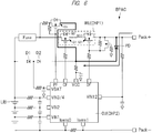
- FIG 4 is a circuit diagram showing a circuit configuration example of the battery pack BPAC.
- the battery pack BPAC includes the lithium ion battery LIB which is an example of a chargeable and dischargeable secondary battery between a positive terminal Pack+ and a negative terminal Pack- of the battery pack BPAC.
- This lithium ion battery LIB is electrically connected to a control unit CU which controls the charge and discharge of the lithium ion battery LIB.
- the control unit CU includes, for example, a control IC, and the lithium ion battery LIB and input terminals (terminals VIN1, VIN2, and VIN3/4) of the control unit CU are electrically connected.
- the terminals (Isens0, Isens1) of the control unit CU are electrically connected to the negative terminal Pack- of the battery pack BPAC.
- the lithium ion battery LIB and the bidirectional connection unit IRU are electrically connected via a fuse (Fuse). Furthermore, the bidirectional connection unit IRU is electrically connected to the positive terminal Pack+ of the battery pack BPAC.
- the bidirectional connection unit IRU includes the discharge power transistor Q1 and the charge power transistor Q2 that are reversely connected in series to each other. In the discharge power transistor Q1, the body diode BD1 is parasitically formed. Likewise, the body diode BD2 is parasitically formed also in the charge power transistor Q2.
- the bidirectional connection unit IRU and the control unit CU are electrically connected. More specifically, a gate of the discharge power transistor Q1 and a terminal CF of the control unit CU are electrically connected, and a gate of the charge power transistor Q2 and a terminal DF of the control unit CU are electrically connected to each other. As a result, the control unit CU controls ON/OFF of charge and discharge currents flowing through the bidirectional connection unit IRU.
- a power supply terminal VCC of the control unit CU is electrically connected to the lithium ion battery LIB via a diode D1 and a diode D2 connected in series. Also, a connection node between the diode D1 and the diode D2 is electrically connected to a terminal VBAT of the control unit CU.
- a protection diode PD is connected between the positive terminal Pack+ of the battery pack BPAC and the power supply terminal VCC of the control unit CU. More specifically, an anode of this protection diode PD is connected to the positive terminal Pack+ of the battery pack BPAC. A cathode of this protection diode PD is connected to the power supply terminal VCC of the control unit CU.
- a normally-on power transistor Q3 of a p-channel field effect transistor is electrically connected to the power supply terminal VCC of the control unit CU.
- This normally-on power transistor Q3 is connected to a connection node between the fuse (Fuse) and the bidirectional connection unit IRU. A gate of the normally-on power transistor Q3 is electrically connected to a terminal PF of the control unit CU. In this manner, the circuit configuration of the battery pack BPAC is made.
- FIG 4 a basic operation of charge and discharge will be described. An operation of connecting a load between the positive terminal Pack+ and the negative terminal Pack- of the battery pack BPAC to flow a discharge current from the lithium ion battery LIB will be described.
- a gate voltage equal to or higher than a threshold voltage is applied from the terminal CF of the control unit CU to the gate of the discharge power transistor Q1
- a gate voltage equal to or higher than the threshold voltage is applied to the gate of the charge power transistor Q2 from the terminal DF of the control unit CU. Accordingly, the discharge power transistor Q1 and the charge power transistor Q2 constituting the bidirectional connection unit IRU are in the ON state.
- the discharge current flows from the lithium ion battery LIB to the positive terminal Pack+ of the battery pack BPAC via the fuse and the bidirectional connection unit IRU.
- a gate voltage lower than the threshold voltage is applied from the terminal CF of the control unit CU to the gate of the discharge power transistor Q1
- a gate voltage lower than the threshold voltage is applied from the terminal DF of the control unit CU to the gate of the charge power transistor Q2.
- the discharge power transistor Q1 and the charge power transistor Q2 constituting the bidirectional connection unit IRU are in the OFF state.
- the discharge current from the lithium ion battery LIB is cut off at the bidirectional connection unit IRU.
- a gate voltage equal to or higher than a threshold voltage is applied from the terminal CF of the control unit CU to the gate of the discharge power transistor Q1
- a gate voltage equal to or higher than the threshold voltage is applied from the terminal DF of the control unit CU to the gate of the charge power transistor Q2. Accordingly, the discharge power transistor Q1 and charge power transistor Q2 constituting the bidirectional connection unit IRU are in the ON state.
- a charge current flows from the positive terminal Pack+ of the battery pack BPAC connected to the charger to the lithium ion battery LIB via the bidirectional connection unit IRU and the fuse.
- a gate voltage lower than the threshold voltage is applied from the terminal CF of the control unit CU to the gate of the discharge power transistor Q1
- a gate voltage lower than the threshold voltage is applied from the terminal DF of the control unit CU to the gate of the charge power transistor Q2.
- the discharge power transistor Q1 and charge power transistor Q2 constituting the bidirectional connection unit IRU are in the OFF state.
- the charge current from the charger is cut off at the bidirectional connection unit IRU.
- FIG 5 is a diagram for explaining the power supply path from the lithium ion battery LIB to the control unit CU during normal operation.
- the path shown below is the power supply path from the lithium ion battery LIB to the control unit CU during normal operation.
- FIG 6 is a diagram for explaining a power supply path from the charger to the control unit CU at the time of precharge.
- FIG 6 there is a path from the positive terminal Pack+ of the battery pack BPAC to the power supply terminal VCC of the control unit CU via the protection diode PD, as the power supply path from the charger to the control unit CU at the time of precharge.
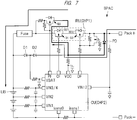
- FIG 7 is a diagram for explaining a current path through which a precharge current from the charger to the lithium ion battery LIB flows at the time of precharge.
- a current path through which the precharge current flows a path flowing from the positive terminal Pack+ of the battery pack BPAC to the lithium ion battery LIB via the bidirectional connection unit IRU and the fuse is conceivable.
- an operating voltage of the control unit CU cannot be obtained sufficiently, especially in an overdischarge state (a state in which a battery voltage is significantly lowered).
- FIG 8 is a diagram for explaining a path where the reverse charging current is cut off.
- a negative potential is applied to the positive terminal Pack+ of the battery pack BPAC
- a positive potential is applied to the negative terminal Pack- of the battery pack BPAC.
- the reverse charging current flowing from the lithium ion battery LIB via the fuse to the bidirectional connection unit IRU is cut off by the body diode BD2 parasitically formed in the charge power transistor Q2 in the bidirectional connection unit IRU.
- the reverse charging current flows from the lithium ion battery LIB to the positive terminal Pack+ of the battery pack BPAC via the diode D1 and the diode D2. Furthermore, the reverse charging current includes reverse charging current flowing to the positive terminal Pack+ of the battery pack BPAC via the normally-on power transistor Q3 and reverse charging current flowing from the power supply terminal VCC of the control unit CU to the positive terminal Pack+ of the battery pack BPAC. These reverse charging currents are cut off by the protection diode PD as shown in FIG 8 . Therefore, in the battery pack BPAC, the function of cutting off the reverse charging current is realized by the body diode BD2 in the bidirectional connection unit IRU and the protection diode PD.
- the battery pack BPAC configured as described above, there is an increasing demand for reducing a thickness of the semiconductor device SA in the battery pack BPAC in order to realize reduction of a thickness of the mobile phone MP and an increase of an occupation rate of the secondary battery in the battery pack BPAC for increasing a charge capacity, for example.
- a technique of embedding the semiconductor chip CHP1, the semiconductor chip CHP2, and the electronic component EPT inside the wiring substrate, as shown in FIG 2 , for example, without providing them on a front surface of the wiring substrate has been studied. This is because such a configuration that components are embedded inside the wiring substrate can make the thickness of the semiconductor device SA smaller than a configuration in which the components are mounted on the front surface of the wiring substrate.
- the semiconductor chip CHP1 in which the bidirectional connection unit IRU is formed has the discharge power transistor Q1 and the charge power transistor Q2 formed therein as shown in FIG 3 .
- the discharge power transistor Q1 and the charge power transistor Q2 are reversely connected in series. Therefore, it is necessary to connect the drain of the discharge power transistor Q1 and the drain of the charge power transistor Q2.
- a back surface electrode made of a metal film is formed on a back surface of the semiconductor chip CHP1.
- the adhesion between the back surface electrode and the embedding member is worse than the adhesion between the silicon and the embedding member.
- FIG 9 is a diagram schematically showing a correspondence relation between the semiconductor chip CHP1 and circuit elements in the first embodiment.
- the semiconductor chip CHP1 according to this first embodiment includes, for example, a semiconductor substrate SUB made of silicon.
- the discharge power transistor Q1 including a power metal oxide semiconductor field effect transistor (MOSFET) and the charge power transistor Q2 including a power MOSFET are formed in this semiconductor substrate SUB.
- an electrode (back surface electrode BE) is formed on a back surface of the semiconductor substrate SUB.
- This back surface electrode BE is connected to the drain of the discharge power transistor Q1 and the drain of the charge power transistor Q2. That is, the back surface electrode BE functions as a common drain electrode.
- an electrode (front surface electrode, source electrode (source pad)) S1 electrically connected to a source of the discharge power transistor Q1 is formed, and an electrode (front surface electrode, gate electrode (gate pad) G1) electrically connected to the gate of the discharge power transistor Q1 is formed.
- an electrode (front surface electrode, source electrode (source pad) S2) electrically connected to the source of the charge power transistor Q2 is formed, and an electrode (front surface electrode, gate electrode (gate pad) G2) electrically connected to the gate of the charge power transistor Q2 is formed.
- the body diode BD1 is parasitically formed in the discharge power transistor Q1 formed in the semiconductor substrate SUB and an anode of the body diode BD1 is electrically connected to the source of the discharge power transistor Q1 as well as a cathode of the body diode BD1 is electrically connected to the drain of the discharge power transistor Q1.
- the body diode BD2 is parasitically formed in the charge power transistor Q2 formed in the semiconductor substrate SUB, and an anode of the body diode BD2 is electrically connected to the source of the charge power transistor Q2 as well as a cathode of the body diode BD2 is electrically connected to the drain of the charge power transistor Q2.
- the discharge power transistor Q1 and the charge power transistor Q2 are formed in the semiconductor chip CHP1 according to this first embodiment, and the discharge power transistor Q1 and the charge power transistor Q2 are reversely connected in series. As a result, the bidirectional connection unit is formed in the semiconductor chip CHP1.
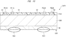
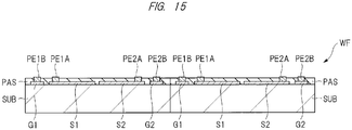
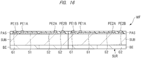
- FIG 10 is a cross-sectional view showing a specific configuration of the semiconductor chip CHP1 according to the first embodiment.
- the semiconductor chip CHP1 according to this first embodiment includes the semiconductor substrate SUB.
- the discharge power transistor (not shown) and the charge power transistor (not shown) reversely connected in series with each other are formed in this semiconductor substrate SUB.
- the back surface electrode BE functioning as the common drain electrode for the discharge power transistor and the charge power transistor is formed on the back surface of the semiconductor substrate SUB.
- an uneven shape RG1 is formed on a front surface of the back surface electrode BE, ie., a surface of the back surface electrode BE opposite to a surface facing the back surface of the semiconductor substrate SUB (or a surface on the same side as the back surface of the semiconductor substrate SUB) (hereinafter referred to as an "exposed surface SUR").
- the source electrode S1 and the gate electrode G1 are formed on the front surface opposite to the back surface of the semiconductor substrate SUB. At this time, the source electrode S1 is electrically connected to the source of the discharge power transistor, and the gate electrode G1 is electrically connected to the gate of the discharge power transistor. Also, on the front surface opposite to the back surface of the semiconductor substrate SUB, the source electrode S2 and the gate electrode G2 are also formed. At this time, the source electrode S2 is electrically connected to the source of the charge power transistor, and the gate electrode G2 is electrically connected to the gate of the charge power transistor. Then, as shown in FIG 10 , a front surface protection film (passivation film, insulating film) PAS is formed so as to cover the front surface of the semiconductor substrate SUB.
- a front surface protection film passivation film, insulating film
- a part of a front surface of the source electrode S1, and a part of a front surface of the source electrode S2 are exposed from the front surface protection film PAS.
- a columnar electrode (pillar electrode) PE1A is formed on the front surface of the source electrode S1 exposed from the front surface protection film PAS.
- a columnar electrode PE2A is formed on the front surface of the source electrode S2 exposed from the front surface protection film PAS.
- a columnar electrode PE1B is formed on the front surface protection film PAS.
- a columnar electrode PE1B is formed on the front surface of the gate electrode G2 exposed from the front surface protection film PAS.
- the semiconductor chip CHP1 includes the semiconductor substrate SUB in which a plurality of power transistors are formed.
- the source electrode (first front surface electrode) S1 electrically connected to the source of the first power transistor (discharge power transistor) out of the plurality of power transistors is formed, and the source electrode (second front surface electrode) S2 electrically connected to the source of the second power transistor (charge power transistor) out of the plurality of power transistors is formed.
- the gate electrode (first control electrode) G1 electrically connected to the gate of the first power transistor (discharge power transistor) is formed, and the gate electrode (second control electrode) G2 electrically connected to the gate of the second power transistor (charge power transistor) is formed.
- the back surface electrode (common drain electrode) BE electrically connected to the drain of the first power transistor (discharge power transistor) and the drain of the second power transistor (charge power transistor) is formed.
- the uneven shape RG1 is formed on the exposed surface (lower surface) SUR of the back surface electrode BE.
- the semiconductor substrate SUB is made of silicon, and inside the semiconductor substrate SUB, an n-type semiconductor region in which n-type impurities such as phosphorus (P) and arsenic (As) are doped into silicon, and a p-type semiconductor region in which p-type impurities such as boron (B) are doped into silicon are formed, for example.
- n-type impurities such as phosphorus (P) and arsenic (As) are doped into silicon
- p-type impurities such as boron (B) are doped into silicon
- the back surface electrode BE is formed, for example, of a layered film including a titanium film (Ti film), a nickel film (Ni film) formed on the titanium film, and a silver film (Ag film) formed on the nickel film.
- Ti film titanium film
- Ni film nickel film
- Ag film silver film
- the back surface electrode BE is not limited thereto.
- a nickel film may be further formed on the silver film, taking into account marking of signs with a laser on the exposed surface SUR of the back surface electrode BE.
- the back surface electrode BE may also be formed of a layered film including a titanium film and a copper film (Cu film).
- the source electrode S1 and the source electrode S2 are formed of, for example, an aluminum film or an aluminum alloy film.
- the gate electrode G1 and the gate electrode G2 are also formed of, for example, an aluminum film or an aluminum alloy film. That is, the source electrodes S1 and S2 and the gate electrodes G1 and G2 are formed of an aluminum film or an aluminum alloy film formed in the same layer.
- a columnar electrode PE1A formed on the source electrode S1, a columnar electrode PE1B formed on the gate electrode G1, a columnar electrode PE2A formed on the source electrode S2, and a columnar electrode PE2B formed on the gate electrode G2 are each mainly composed of a copper film.
- the front surface protection film PAS is constructed of an insulating film such as a silicon oxide film or a silicon nitride film, for example.
- a thickness of the semiconductor substrate SUB is, for example, substantially 100 ⁇ m to 200 ⁇ m.
- a thickness of each of the source electrodes S1 and S2 and the gate electrodes G1 and G2 formed on the front surface of the semiconductor substrate SUB is, for example, substantially 4 ⁇ m to 5 ⁇ m.
- a thickness of the back surface electrode BE formed on the back surface of the semiconductor substrate SUB is, for example, substantially 10 ⁇ m to 30 ⁇ m.
- a difference (unevenness) between a top and a bottom of a projection of the uneven shape RG1 formed on the exposed surface SUR of the back surface electrode BE is, for example, substantially 3 ⁇ m to 5 ⁇ m.
- the thickness of the back surface electrode BE is larger than the thickness of each of the source electrodes S1 and S2 and the gate electrodes G1 and G2.
- a surface roughness of the exposed surface SUR of the back surface electrode BE where the uneven shape RG1 is formed is rougher than a surface roughness of the front surface of each of the source electrodes S1 and S2 and the gate electrodes G1 and G2. That is, in this first embodiment, the uneven shape is intentionally formed on the exposed surface SUR of the back surface electrode BE, whereas an uneven shape is not intentionally formed on the front surface of each of the source electrodes S1 and S2 and the gate electrodes G1 and G2.
- the uneven shape formed on the front surface of each of the source electrodes S1 and S2 and the gate electrodes G1 and G2 is smaller than the uneven shape RG1 intentionally formed on the exposed surface SUR of the back surface electrode BE.
- the uneven shape RG1 intentionally formed on the exposed surface SUR of the back surface electrode BE is larger than the uneven shape formed on the front surface of each of the source electrodes S1 and S2 and the gate electrodes G1 and G2.
- the semiconductor chip CHP1 according to this first embodiment is configured.
- the discharge power transistor Q1 and the charge power transistor Q2 formed of a vertical transistor flowing current in a thickness direction of the semiconductor chip CHP1 are formed. More specifically, in FIG 9 , the discharge power transistor Q1 is formed in the left side region of a center line CL. The charge power transistor Q2 is formed in the right side region of the center line CL.
- the back surface electrode BE shown in FIG 9 functions as the drain of the discharge power transistor Q1 formed in the left side region of the center line CL and also functions as the drain of the charge power transistor Q2 formed in the right side region of the center line CL.
- the drain of the discharge power transistor Q1 and the drain of the charge power transistor Q2 formed in the semiconductor chip CHP1 are electrically connected.
- the device structure of the discharge power transistor Q1 is equal to the device structure of the charge power transistor Q2. Therefore, in the following description, for example, the device structure of the power transistor will be described focusing on the discharge power transistor Q1.
- the discharge power transistor Q1 is configured by connecting several thousands to hundreds of thousands of unit transistors (cell transistors) in parallel. In FIG 11 described below, the device structure of the discharge power transistor Q1 will be described by taking two adjacent unit transistors as an example.
- FIG 11 is a cross-sectional view showing an example of the device structure of the unit transistor formed in a cell forming region.
- an epitaxial layer EPI is formed on a substrate layer 1S made of silicon containing n-type impurities such as phosphorus (P) and arsenic (As).
- This epitaxial layer EPI is formed of a semiconductor layer containing silicon as a main component into which n-type impurities such as phosphorus (P) and arsenic (As) are doped, for example.
- the substrate layer 1S and the epitaxial layer EPI are components functioning as the drains of the power transistors (discharge power transistor Q1 and charge power transistor Q2). Note that, in this first embodiment, as shown in FIG 11 , combination of the substrate layer 1S and the epitaxial layer EPI is referred to as the semiconductor substrate SUB.
- an element portion is formed in a front surface of the epitaxial layer EPI. More specifically, in the element portion according to this first embodiment, a channel region CH is formed in the front surface of the epitaxial layer EPI. A trench TR penetrating this channel region CH and reaching the epitaxial layer EPI is formed. At this time, a gate insulating film GOX is formed on an inner wall of the trench TR. A gate GE is formed so as to bury the trench TR over this gate insulating film GOX.
- the gate insulating film GOX is formed of, for example, a silicon oxide film, but the gate insulating film GOX is not limited thereto.
- the gate insulating film GOX may be formed of a high dielectric constant film having a dielectric constant higher than, for example, a silicon oxide film. Further, the gate GE is formed of, for example, a polysilicon film.
- a source region SR is formed in a front surface of the channel region CH adjacent to the trench TR.
- An insulating film BPSG is formed over an upper surface of the trench RE in which the gate GE is embedded and over the source region SR.
- the channel region CH includes a semiconductor region into which p-type impurities such as boron (B) are doped, for example, and the source region SR includes a semiconductor region into which n-type impurities such as phosphorus (P) and arsenic (As) are doped, for example.
- This body contact region BC includes a semiconductor region into which p-type impurities such as boron (B) are doped, for example, and an impurity concentration of the body contact region BC is higher than an impurity concentration of the channel region CH.
- a plug PLG1 made of a barrier conductor film BCF and a tungsten film is formed so as to bury the groove having the body contact region BC formed at the bottom thereof
- the barrier conductor film BCF and the aluminum alloy film AF are formed over an insulating film BPSG
- the aluminum alloy film AF is electrically connected with the source region SR and also electrically connected with the channel region CH via the body contact region BC. That is, the aluminum alloy film AF shown in FIG 11 constitutes, for example, the source electrode S1 (the source electrode S2) shown in FIG 10 .
- the body contact region BC has a function of securing ohmic contact with the plug PLG1. Due to presence of this body contact region BC, the source region SR and the channel region CH are electrically connected at the same potential.
- the source region SR as an emitter region
- the channel region CH as a base region
- the epitaxial layer EPI as a collector region. That is, the fact that the source region SR and the channel region CH are electrically connected at the same potential means that there is no potential difference between the emitter region and the base region of the parasitic npn bipolar transistor, so that this can suppress the ON operation of the parasitic npn bipolar transistor.
- the back surface electrode BE is formed On the exposed surface SUR of this back surface electrode BE, the uneven shape RG1 intentionally formed is present.
- the device structure of the power transistor (the discharge power transistor Q1 or the charge power transistor Q2) is formed inside the semiconductor chip CHP1 according to the present embodiment
- the body diode which is a parasitic diode is formed by the epitaxial layer EPI which is an n-type semiconductor layer and the channel region CH which is a p-type semiconductor layer. That is, the body diode which is a pn junction diode having the channel region CH as the anode and the epitaxial layer EPI as the cathode is formed between the epitaxial layer EPI and the channel region CH.
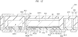
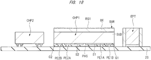
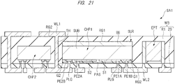
- FIG 12 is a cross-sectional view showing a configuration of a semiconductor device SA1 according to the first embodiment.
- a plurality of electronic components including a semiconductor component are mounted on a substrate 2S. More specifically, the semiconductor chip CHP1, the semiconductor chip CHP2, and the electronic component EPT such as a capacitor or a resistive element are mounted over the substrate 2S.
- the semiconductor device SA1 according to this first embodiment includes, for example, the semiconductor chip CHP1 in which the bidirectional connection unit IRU shown in FIG 4 is formed, the semiconductor chip CHP2 in which the control unit CU is formed, and the electronic component EPT including other passive components. Therefore, the semiconductor device SA1 according to this first embodiment is a semiconductor device controlling charge and discharge of the lithium ion battery LIB which is an example of a chargeable and dischargeable secondary battery.
- the semiconductor chip CHP1 is connected with the substrate 2S in a state in which a front surface of the semiconductor chip CHP1 faces an upper surface of the substrate 2S (facedown mounting). More specifically, the semiconductor chip CHP1 is mounted over the substrate 2S such that each of a columnar electrode PE1A formed on the source electrode S1, a columnar electrode PE1B formed on the gate electrode G1, a columnar electrode PE2A formed on the source electrode S2, and a columnar electrode PE2B formed on the gate electrode G2 is connected to a terminal (not shown) formed in the substrate 2S. Similarly, the semiconductor chip CHP2 is connected with the substrate 2S in a state in which a front surface of the semiconductor chip CHP2 faces the upper surface of the substrate 2S. In addition, the electronic component EPT is mounted over the substrate 2S such that a terminal of the electronic component EPT is connected to a terminal of the substrate 2S.
- a plug PLG that electrically connects with a terminal formed in the upper surface of the substrate 2S is formed so as to penetrate the substrate 2S.
- a plurality of wirings WL2 are formed on a lower surface of the substrate 2S, and the plug PLG and the wiring WL2 are electrically connected. Therefore, the terminal formed in the upper surface of the substrate 2S and the wiring WL2 formed on the lower surface of the substrate 2S are electrically connected via the plug PLG
- a resin sealing member R1 is formed so as to cover the semiconductor chip CHP1, the semiconductor chip CHP2, and the electronic component EPT mounted over the upper surface of the substrate 2S.
- a through hole TH is formed so as to penetrate the resin sealing member R1 and the substrate 2S.
- a plurality of wirings WL1 are formed on a front surface of the resin sealing member R1. This wiring WL1 is electrically connected with the wiring WL2 formed on the lower surface of the substrate 2S via the through hole TH.
- the semiconductor chip CHP1, the semiconductor chip CHP2, and the electronic component EPT are embedded inside a wiring substrate WB including the substrate 2S and the resin sealing member R1.
- the back surface electrode BE formed in the semiconductor chip CHP1 is in contact with the resin sealing member R1.
- a surface of the back surface electrode BE which is in contact with the resin sealing member R1 has the uneven shape RG1.
- the uneven shape RG2 is also formed on a surface of the wiring WL1 in contact with of the resin sealing member R1.
- the uneven shape RG2 is also formed on a surface of the wiring WL1 in contact with of the resin sealing member R1.
- a surface roughness of the surface, which is in contact with the resin sealing member R1, of the back surface electrode BE where the uneven shape RG1 is formed is equivalent to a surface roughness of the front surface of each of the wiring WL1 and the wiring WL2 where the uneven shape RG2 is formed.
- the difference (unevenness) between the top and the bottom of the projection of the uneven shape RG1 formed on the back surface electrode BE is equivalent to difference between a top and a bottom of a projection of the uneven shape RG2 formed on the wiring WL1 and the wiring WL2.
- the uneven shape RG1 is always formed on the surface, which is in contact with the resin sealing member R1, of the back surface electrode BE, while the wiring WL1 and the wiring WL2 do not necessarily have the uneven shape RG2 formed thereon. Therefore, in this case, it can be said that the surface roughness of the surface, which is in contact with the resin sealing member R1, of the back surface electrode BE where the uneven shape RG1 is formed is rougher than the surface roughness of each of the front surface of the wiring WL1 and the front surface of the wiring WL2.
- an external size of the semiconductor chip CHP1 is larger than an external size of the semiconductor chip CHP2, and in particular, a thickness of the semiconductor chip CHP1 is larger than a thickness of the semiconductor chip CHP2.
- the power transistor is formed in the semiconductor chip CHP1
- an integrated circuit such as a logic circuit as a representative is formed in the semiconductor chip CHP2. That is, several thousands to several hundreds of thousands of unit transistors are formed in the semiconductor chip CHP1, and a thick epitaxial layer is formed in order to secure a withstand voltage. Therefore, the semiconductor chip CHP1 has a larger external size than the semiconductor chip CHP2 in which an integrated circuit with low power consumption such as a logic circuit as a representative is formed.
- the semiconductor chip CHP1 in which the power transistor is formed handles a larger current than the semiconductor chip CHP2 in which the integrated circuit is formed and needs to ensure a higher withstand voltage than the semiconductor chip CHP2. Therefore, the external size of the semiconductor chip CHP1 is larger than the external size of the semiconductor chip CHP2.
- the thickness of the back surface electrode BE formed in the semiconductor chip CHP1 is substantially the same as a thickness of the wiring WL and a thickness of the wiring WL2 formed in the wiring substrate WB.
- the back surface electrode BE formed in the semiconductor chip CHP1 is formed of a layered film of a titanium film, a nickel film, and a silver film, but is not limited thereto.
- the back surface electrode BE formed in the semiconductor chip CHP1 can also be formed of a layered film of a titanium film and a copper film which is the same material as the wiring WL1 and the wiring WL2. That is, metal films with low resistivity can be widely applied to the back surface electrode BE.
- the first feature point of this first embodiment is in that, for example, as shown in FIG 12 , the semiconductor chip CHP1 in which the power transistor is formed is embedded inside the wiring substrate WB.
- the semiconductor device SA1 can be made thinner than a configuration in which the semiconductor chip CHP1 is mounted on the wiring substrate WB.
- a thickness of the entire semiconductor device including the wiring substrate WB and the semiconductor chip CHP1 is a sum of a thickness of the wiring substrate WB itself and the thickness of the semiconductor chip CHP1, and furthermore, considering that it is necessary to seal the semiconductor chip CHP1 with a sealing member, a thickness of the sealing member covering the semiconductor chip CHP1 is also added.
- a thickness of the sealing member covering the semiconductor chip CHP1 is also added.
- the semiconductor chip CHP1 in which a power transistor is formed is embedded inside the wiring substrate WB (first feature point).
- the thickness of the entire semiconductor device SA1 according to this first embodiment is equivalent to the thickness of the wiring substrate WB, which makes it possible to reduce the thickness of the semiconductor device SA1.
- the wiring substrate WB itself functions as a sealing member covering the semiconductor chip CHP1.
- the semiconductor device SA1 according to this first embodiment there is no need to newly provide a sealing member covering the semiconductor chip CHP1. Therefore, according to this first embodiment, there is no need to consider a thickness of a sealing member to be newly formed, and the semiconductor device SA1 can be made thinner by a thickness equivalent to the thickness of this sealing member.
- the thickness of the semiconductor device SA1 can be defined only by the thickness of the wiring substrate WB, almost irrespective of the thickness of the semiconductor chip CHP1, which makes it possible to reduce the thickness of the semiconductor device SA1.
- the wiring substrate WB itself functions as a sealing member for protecting the semiconductor chip CHP1, and this eliminates the necessity of providing a new sealing member for sealing the semiconductor chip CHP1.
- a secondary effect since there is no need to use a new sealing member, an effect that manufacturing costs of the semiconductor device SA1 can be reduced is also obtained.
- the semiconductor device SA1 due to a synergistic effect resulting from the direct effect and the indirect effect caused by embedding the above-mentioned semiconductor chip CHP1 inside the wiring substrate WB, it is possible to obtain a remarkable effect that the semiconductor device SA1 can be made thinner. As a result, for example, by using the semiconductor device SA1 of this first embodiment for a battery pack, it is possible to realize a thinner battery pack. Thus, according to this first embodiment, it is possible to provide the semiconductor device SA1 that contributes to thinning of a mobile phone and an increase in occupation ratio of a secondary battery in a battery pack for increasing a charge capacity.
- the following advantages can also be obtained.
- an electronic component including the semiconductor chip CHP1 is mounted on the front surface of the wiring substrate WB, it is necessary to form an underfill resin or a fillet of a solder material in order to improve connection reliability between the wiring substrate WB and the electronic component.
- the electronic component is embedded inside the wiring substrate WB, and in this case, it is not necessary to form the underfill resin or the fillet of the solder material. Therefore, according to this first embodiment, it is unnecessary to secure the region for forming the underfill resin or the fillet of the solder material, and as a result, the size of the semiconductor device SA1 can be reduced. That is, the first feature point of this first embodiment is useful for not only reducing the thickness of the semiconductor device SA1 but also reducing the size of the semiconductor device SA1.
- the second feature point of this first embodiment is in that, for example, as shown in FIG 12 , the back surface electrode BE is formed on the back surface of the semiconductor chip CHP1 in which the power transistor is formed, and the thickness of the back surface electrode BE is larger than the thickness of each of the source electrodes S1 and S2 formed on the front surface of the semiconductor chip CHP1. As a result, it is possible to reduce ON resistance of the power transistor formed in the semiconductor chip CHP1.
- the bidirectional connection unit is formed in the semiconductor chip CHP1 according to this first embodiment and includes the discharge power transistor and the charge power transistor reversely connected in series with each other. That is, since the discharge power transistor and the charge power transistor are reversely connected in series, the drain of the discharge power transistor and the drain of the charge power transistor are electrically connected. That is, in this first embodiment, due to the epitaxial layer which functions as the drain of the discharge power transistor and also as the drain of the charge power transistor, the drain of the discharge power transistor and the drain of the charge power transistor are electrically connected. However, since the epitaxial layer is the semiconductor layer, the ON resistance becomes large when the drain of the discharge power transistor and the drain of the charge power transistor are electrically connected only by the epitaxial layer.
- the back surface electrode BE formed of, for example, a low resistance metal film is formed on the back surface of the semiconductor chip CHP1.
- the drain of the discharge power transistor and the drain of the charge power transistor are electrically connected not only by the epitaxial layer but also by the low resistance back surface electrode BE, so that the ON resistance can be reduced.
- the thickness of the back surface electrode BE is increased in order to increase an effect of reducing the ON resistance. This is because, as the thickness of the back surface electrode BE is increased, the resistance of the back surface electrode BE decreases. More specifically, in this first embodiment, the thickness of the back surface electrode BE is larger than the thickness of each of the source electrodes S1 and S2 formed on the front surface of the semiconductor chip CHP1. Thus, the ON resistance of the semiconductor chip CHP1 functioning as a bidirectional connection unit can be reduced. However, from the viewpoint of reducing the ON resistance, it is desirable to increase the thickness of the back surface electrode BE.
- the thickness of the back surface electrode BE is made too large, the wiring substrate WB tends to warp due to difference in linear expansion coefficient from the wiring substrate WB in which the semiconductor chip CHP1 is embedded.
- the thickness of the back surface electrode BE is made to be smaller than substantially 30 ⁇ m in order to suppress warpage occurring in the wiring substrate WB.
- the semiconductor device SA1 of this first embodiment has the above-described first feature point and second feature point, which makes it possible to improve performance of the semiconductor device SA1 by reducing the thickness and the size of the semiconductor device SA1 and reducing the ON resistance of the semiconductor device SA1.
- the back surface electrode BE is peeled off from the embedding member, resulting in reduction in reliability of the semiconductor device SA1.
- this peeling is likely to be caused by the fact that the adhesion between the back surface electrode BE and the embedding material is not so good and by the fact that, for example, as shown in FIG 12 , the external size of the semiconductor chip CHP1 is larger than the external size of the semiconductor chip CHP2.
- the peeling between the back surface electrode BE and the wiring substrate WB is likely to become apparent. That is, in the semiconductor chip CHP1 in which the power transistor is formed, peeling from the wiring substrate is likely to be more apparent than the semiconductor chip CHP2 because the back surface electrode BE having poor adhesion to the embedding material is formed on the back surface of the semiconductor chip CHP1, the thickness of the back surface electrode BE is formed to be large, and the external size of the semiconductor chip CHP1 becomes large.
- the third feature point according to this first embodiment is in that, for example, as shown in FIG 12 , the uneven shape RG1 is intentionally formed on the surface of the back surface electrode BE which is in contact with the embedding member (wiring substrate WB).
- the adhesion between the back surface electrode BE and the wiring substrate WB can be improved by an anchor effect caused by the uneven shape RG1 formed on the back surface electrode BE.
- peeling of the semiconductor chip CHP1 from the wiring substrate WB is effectively suppressed by improving the adhesion between the back surface electrode BE and the wiring substrate WB, whereby the reliability of the semiconductor device SA1 can be improved.
- the uneven shape RG1 formed on the back surface electrode BE preferably has a large difference between the top and the bottom of the projection. More specifically, the difference (unevenness) between the top and the bottom of the projection of the uneven shape RG1 can be substantially 3 ⁇ m to 5 ⁇ m.
- the uneven shape RG2 may also be formed on the wiring WL1 and the wiring WL2 formed in the wiring substrate WB. In this case, the uneven shape RG1 formed on the back surface electrode BE can be equivalent to the uneven shape RG2 formed on the wiring WL1 and the wiring WL2.
- the wiring WL1 and the wiring WL2 formed in the wiring substrate WB are made of materials having good adhesion from the viewpoint of improving the adhesion to the wiring substrate WB (epoxy resin). Therefore, when the material of the back surface electrode BE formed on the back surface of the semiconductor chip CHKP1 is made of the same material as the materials of the wiring WL1 and the wiring WL2, the adhesion to the wiring substrate WB can be further improved.
- the wiring WL1 and the wiring WRL2 are formed of a layered film including a titanium film and a copper film.
- the back surface electrode BE can be also formed of a layered film including a titanium film and a copper film.
- the copper constituting the copper film has an electrical resistivity as low as that of silver and is cheaper than silver, so that it is also possible to reduce the manufacturing costs of the semiconductor device SA1.
- FIG 13 illustrates a chip forming region CR1 and a chip forming region CR2 included in the semiconductor wafer WF.
- the following device structure has already been formed by a device forming process executed before the process to be described. That is, in the semiconductor wafer WF, both the discharge power transistor and the charge power transistor which are reversely connected in series with each other are formed in the semiconductor substrate SUB of each of the chip forming region CR1 and the chip forming region CR2.
- the source electrode S1 electrically connected to the source of the discharge power transistor and the gate electrode G1 electrically connected to the gate of the discharge power transistor are formed on the front surface of the semiconductor substrate SUB of each of the chip forming region CR1 and the chip forming region CR2.
- the source electrode S2 electrically connected to the source of the charge power transistor and the gate electrode G2 electrically connected to the gate of the charge power transistor are formed on the front surface of the semiconductor substrate SUB of each of the chip forming region CR1 and the chip forming region CR2.
- a front surface protection film PAS is formed so as to cover the source electrodes S1 and S2 and the gate electrodes G1 and G2, and the front surface protection film PAS has an opening portion OP which exposes a part of the front surface of each of the source electrodes S1 and S2 and the gate electrodes G1 and G2 formed therein.
- a columnar electrode (Cu pillar electrode) is formed so as to fill the opening portion OP formed in the front surface protection film PAS. More specifically, a columnar electrode PElAis formed on the front surface of the source electrode S1 exposed in the opening portion OP, and a columnar electrode PE1B is formed on the front surface of the gate electrode G1 exposed in the opening portion OP. Likewise, a columnar electrode PE2A is formed on the front surface of the source electrode S2 exposed in the opening portion OP, and a columnar electrode PE2B is formed on the front surface of the gate electrode G2 exposed in the opening portion OP. These columnar electrodes PE1A to PE2B have a columnar shape made of copper having a height of substantially 10 ⁇ m to 20 ⁇ m.
- the back surface of the semiconductor substrate SUB is ground as shown in FIG 15 . More specifically, for example, the back surface of the semiconductor substrate SUB is ground such that the thickness of the semiconductor substrate SUB becomes substantially 100 ⁇ m to 200 ⁇ m.
- the back surface electrode BE is formed on the back surface of the semiconductor substrate SUB.
- This back surface electrode BE is formed of, for example, a layered film including a titanium film, a nickel film, and a silver film, or a layered film including a titanium film and a copper film, and can be formed by sputtering or plating, for example.
- the material constituting the back surface electrode BE is not limited thereto.
- the wiring formed in the wiring substrate is formed of the copper film in consideration of improvement of the adhesion to the wiring substrate, it is desirable to form the back surface electrode BE with a copper film from the viewpoint of improving the adhesion between the back surface electrode BE and the wiring substrate when buried in the wiring substrate.
- the back surface electrode BE functions as the common drain electrode for the discharge power transistor and the charge power transistor reversely connected in series with each other. Therefore, in order to reduce the ON resistance, the back surface electrode BE is formed thicker than the thickness of the source electrode S1 and the source electrode S2 formed on the front surface of the semiconductor substrate SUB. Accordingly, resistance of the back surface electrode BE can be reduced. As a result, it is possible to reduce ON resistance generated when the charge and discharge currents flow between the discharge power transistor and the charge power transistor reversely connected in series with each other.
- the uneven shape RG1 is formed on the exposed surface (lower surface) SUR of the back surface electrode BE.
- the exposed surface SUR of the back surface electrode BE is subjected to wet etching using a chemical solution, so that the uneven shape RG1 can be formed.
- a chemical solution that roughens the exposed surface SUR of the back surface electrode BE is sprayed, so that the uneven shape RG1 can be formed quickly and easily on the exposed surface SUR of the back surface electrode BE.
- a chemical solution that roughens the copper film constituting the back surface electrode BE is often used for wiring formed in the wiring substrate, and it is possible to easily select chemical solutions of various specifications.
- the semiconductor wafer WF is cut into a plurality of semiconductor chips CHP1 by dicing. For example, by dicing at a portion between the chip forming region CR1 and the chip forming region CR2 shown in FIG 17 , the chip forming region CR1 and the chip forming region CR2 are cut apart, and as a result, a semiconductor chip including the separated chip forming region CR1 and a semiconductor chip including the separated chip forming region CR2 are obtained. After that, the singulated semiconductor chip CHP1 goes through necessary inspections such as an electrical characteristic inspection and a visual inspection, and then, the singulated semiconductor chip CHP1 is packed by a tape storage, a tray storage, or the like to be shipped out
- the manufacturing method of a semiconductor device according to this first embodiment includes various manufacturing methods, and the manufacturing method of the semiconductor device indicated below is one example and is not limited thereto.
- a substrate 2S is prepared, and a plurality of electronic components are prepared. More specifically, the plurality of electronic components include a semiconductor chip CHP1 functioning as a bidirectional connection unit through which charge and discharge currents flow, a semiconductor chip CHP2 functioning as a control unit controlling charge/discharge of a secondary battery, and an electronic component EPT formed of a passive component such as a capacitor or a resistive element
- the semiconductor chip CHP1, the semiconductor chip CHP2, and the electronic component EPT are mounted over the substrate 2S. That is, a plurality of terminals are formed in a front surface of the substrate 2S, and the semiconductor chip CHP1, the semiconductor chip CHP2, and the electronic component EPT are mounted over the substrate 2S such that the plurality of terminals are electrically connected with the semiconductor chip CHP1, the semiconductor chip CHP2, and the electronic component EPT.
- the semiconductor chip CHP1 when the semiconductor chip CHP1 is focused, the semiconductor chip CHP1 is mounted over the substrate 2S in a state in which the front surface of the semiconductor chip CHP1 faces downward such that columnar electrodes PE1A to PE2B formed in the semiconductor chip CHP1 and the terminals formed in the substrate 2S are connected to each other. Therefore, a back surface of the semiconductor chip CHP1 on which a back surface electrode BE is formed will face upward.
- the semiconductor chip CHP1, the semiconductor chip CHP2, and the electronic component EPT mounted over the substrate 2S are covered (sealed) with an insulating resin sealing member R1.
- the resin sealing member R1 used in this first embodiment is made of an epoxy resin material, for example.
- the semiconductor chip CHKP2 and the electronic component EPT are embedded in the wiring substrate WB made of the substrate 2S and the resin sealing member R1.
- the back surface electrode BE formed on the back surface of the semiconductor chip CHP1 comes into contact with the resin sealing member R1.
- the uneven shape RG1 is formed on the back surface electrode BE, the adhesion between the back surface electrode BE and the resin sealing member R1 due to the anchor effect caused by the uneven shape RG1 can be improved.
- holes are formed in the substrate 2S, for example, by using a laser. Thereafter, for example, by using a plating method, a copper film is embedded in this hole to form a via VA.
- a manufacturing method of a battery pack (electronic device) according to this first embodiment will be described.
- a chargeable and dischargeable secondary battery for example, a lithium ion battery
- a semiconductor device SA1 according to this first embodiment which controls this secondary battery is prepared. Then, by electrically connecting the secondary battery and the semiconductor device SA1, a battery pack according to this first embodiment can be manufactured.
- a discharge power transistor and a charge power transistor are formed in a semiconductor chip in which a bidirectional connection unit is formed.
- each of the discharge power transistor and the charge power transistor includes several thousands to hundreds of thousands of unit transistors connected in parallel with each other.
- a magnitude of the charge and discharge currents flowing through the discharge power transistor and the charge power transistor is increased in accordance with increase in the charge capacity of the secondary battery.
- increase of the allowable current of the discharge power transistor and the charge power transistor and reduction of the ON resistance are considered, it is necessary to increase the number of unit transistors constituting each of the discharge power transistor and the charge power transistor.
- a size of the chip mounting portion having a semiconductor chip in which a power transistor is formed mounted thereon is usually larger than the size of the semiconductor chip in view of flowing a large current and improving heat dissipation efficiency (large tab structure).
- the size of the semiconductor chip is increased, it is necessary to further increase the size of the chip mounting portion so as to have the larger semiconductor chip disposed inside the chip mounting portion in a plan view. In other words, it is necessary to increase the size of the chip mounting portion such that the back surface of the semiconductor chip is not exposed from the chip mounting portion. That is, in this structure (large tab structure), the size of the chip mounting portion must also be increased according to increase in the size of the semiconductor chip, resulting in significant increase in the size of the semiconductor device SA1.
- the second embodiment adopts a configuration in which, in consideration of increase of the allowable current and reduction of the ON resistance, the external size of the semiconductor chip is increased and the external size of the chip mounting portion is maintained as it is.
- the external size of the semiconductor chip is increased, while the external size of the chip mounting portion is maintained as it is. Therefore, as shown in FIG 22 , the external size of the semiconductor chip inevitably becomes larger than the external size of the chip mounting portion.
- the semiconductor chip has a portion (protruding portion) protruding from the chip mounting portion.
- the inventor of the present application found that new matters to be improved arise due to the presence of the portion protruding from the chip mounting portion. That is, the portion protruding from the chip mounting portion comes into contact with the sealing body. That is, in the portion of the semiconductor chip protruding from the chip mounting portion, the back surface electrode formed in the semiconductor chip is in contact with the sealing body. At this time, the adhesion between the back surface electrode and the sealing body is not good. Therefore, in the portion protruding from the chip mounting portion, peeling tends to occur between the back surface electrode and the sealing body, and as a result, it is concerned that reliability of the semiconductor device may be reduced.
- FIG 22 is a cross-sectional view showing a configuration of a semiconductor device SA2 according to a second embodiment.
- the semiconductor device SA2 according to this second embodiment includes a chip mounting portion (component mounting portion) TAB and a lead LD1 and a lead LD2 arranged outside the chip mounting portion TAB.
- a semiconductor chip CHP1 having a bidirectional connection unit formed therein is mounted over the chip mounting portion TAB via an adhesive ADH.
- the chip mounting portion TAB is disposed inside the semiconductor chip CHP1 (small tab structure). That is, as shown in FIG 22 , the external size of the semiconductor chip CHP1 is larger than the external size of the chip mounting portion TAB, and the semiconductor chip CHP1 has a portion protruding from an outer edge portion of the chip mounting portion TAB.
- a back surface electrode BE is formed on a back surface of the semiconductor chip CHP1, and an uneven shape RG1 is formed on an exposed surface (lower surface) SUR of the back surface electrode BE. Therefore, the uneven shape RG1 formed on the back surface electrode BE comes in contact with the adhesive ADH.
- the source electrodes S1 and S2 and the gate electrodes G1 and G2 are formed on a front surface of the semiconductor chip CHP1.
- a columnar electrode PE1A is formed on the source electrode S1, and a columnar electrode PE1B is formed on the gate electrode G1.
- a columnar electrode PE2A is formed on the source electrode S2, and a columnar electrode PE2B is formed on the gate electrode G2.
- the columnar electrode PE1B and the lead LD2 are electrically connected by a wire W
- the columnar electrode PE2B and the lead LD1 are electrically connected by a wire W
- a sealing body MR made of, for example, a silica-based filler and a thermosetting epoxy resin is formed so as to cover the semiconductor chip CHP1 and the wire W
- a portion protruding from the chip mounting portion TAB is formed in the semiconductor chip CHP1. Therefore, in this protruding portion, the uneven shape RG1 formed on the back surface electrode BE comes into contact with the sealing body MR In this manner, the semiconductor device SA2 according to this second embodiment is configured.
- a feature point according to the second embodiment is in that, for example, as shown in FIG 22 , an uneven shape RG1 is intentionally formed on the entire lower surface of the back surface electrode BE.
- the adhesion between the back surface electrode BE and the sealing body MR can be improved by the anchor effect due to the uneven shape RG1 formed on the back surface electrode BE, in the portion protruding from the outer edge portion of the chip mounting portion TAB.
- peeling of the semiconductor chip CHP1 from the sealing body MR is effectively suppressed by improving the adhesion between the back surface electrode BE and the sealing body MR, whereby reliability of the semiconductor device SA2 can be improved.
- reliability of the semiconductor device SA2 can be improved.
- the first modification of the second embodiment will be hereinafter described. That is, in the second embodiment, a description has been given regarding an example in which the technical idea according to the first embodiment is applied to the semiconductor chip CHP1 in which a discharge power transistor and a charge power transistor constituting a bidirectional connection unit are formed.
- the embodiment is not limited thereto, but the technical idea in the first embodiment can be applied to a semiconductor chip in which one power transistor is formed.
- the film thickness of the back surface electrode is formed larger than a film thickness of the source electrode formed on a front surface of the semiconductor chip. This makes it possible to reduce the resistance value of the current path that bypasses the portion protruding from the chip mounting portion.
- the film thickness of the back surface electrode is particularly large.
- the same technical idea as in the second embodiment is applied to the semiconductor chip in which one power transistor is formed, so that the portion protruding from the chip mounting portion can also be effectively utilized as a current path having a low resistance value. Furthermore, it is possible to improve the adhesion between the portion protruding from the chip mounting portion and the sealing body. That is, according to this first modification, it is possible to obtain such a remarkable effect that performance improvement can be achieved by increasing the allowable current in the semiconductor device and by reducing the ON resistance and that it is possible to improve reliability of the semiconductor device by improving the adhesion between the portion protruding from the chip mounting portion and the sealing body.
- the first modification is applied to the power MOSFET as an example of one power transistor.
- the technical idea according to the second embodiment is not limited to the power MOSFET, but may also be widely applied to, for example, a semiconductor device having a semiconductor chip in which one insulated gate bipolar transistor (IGBT) is formed
- the semiconductor chip includes: a semiconductor substrate in which an insulated gate bipolar transistor is formed; and a first front surface electrode (emitter electrode, emitter pad) formed on a first surface of the semiconductor substrate and electrically connected to the insulated gate bipolar transistor. Further, the semiconductor chip includes: a second front surface electrode (gate electrode, gate pad) formed on the first surface of the semiconductor substrate and electrically connected to the insulated gate bipolar transistor; and a back surface electrode (collector electrode) formed on a second surface opposite to the first surface of the semiconductor substrate and electrically connected to the insulated gate bipolar transistor. At this time, an uneven shape is formed on an exposed surface of the back surface electrode.
- the first modification is applied to the power MOSFET.
- the technical idea according to the second embodiment is not limited to the power MOSFET, but may also be widely applied to, for example, a semiconductor device having a semiconductor chip in which one diode is formed.
- the semiconductor chip includes a semiconductor substrate having a diode formed therein; a first front surface electrode (anode electrode, anode pad) formed on a first surface of the semiconductor substrate and electrically connected to the diode; and a back surface electrode (cathode electrode) formed on a second surface opposite to the first surface of the semiconductor substrate and electrically connected to the diode. At this time, an uneven shape is formed on the exposed surface of the back surface electrode.
- FIG 23(a) is a plan view seen from a lower surface of a semiconductor device SA3 according to the third embodiment.
- the semiconductor device SA3 according to the third embodiment includes, for example, a rectangular substrate WB.
- a source pad SP, a gate pad GP, and a drain pad DP are formed on the same surface of the substrate WB.
- FIG 23(b) is a cross-sectional view taken along a line A-A of FIG 23(a) .
- the semiconductor chip CHP1 is embedded in the substrate WB.
- a source electrode SE and a gate electrode GE are formed on a front surface (on the lower surface side in FIG 23 ) of the semiconductor chip CHP1, and on a back surface (upper surface side in FIG 23 ) of the semiconductor chip CHP1, a back surface electrode BE is formed.
- a columnar electrode PLR1 electrically connected to the source electrode SE is formed, and a columnar electrode PLR2 electrically connected to the gate electrode GE is formed.
- the columnar electrode PLR1 is electrically connected to the source pad SP formed on the lower surface of the substrate WB via a plug PLG1 formed on the substrate WB.
- the columnar electrode PLR2 is electrically connected to the gate pad GP formed on the lower surface of the substrate WB via a plug PLG2 formed in the substrate WB.
- the back surface electrode BE formed on the back surface of the semiconductor chip CHP1 is electrically connected to a drain wiring DL formed on the upper surface of the substrate WB via a plug PLG3 formed on the upper surface side of the substrate WB.
- the drain wiring DL is electrically connected to the drain pad DP formed on the lower surface of the substrate WB via a plug PLG4 penetrating the substrate WB.
- the semiconductor device SA3 of the third embodiment for example, the semiconductor device SA3 is mounted such that the lower surface of the semiconductor device SA3 faces a mounting board, so that each of the source pad SP, the gate pad GP, and the drain pad DP is electrically connected to a terminal formed in the mounting board
- the back surface electrode BE is formed on the back surface of the semiconductor chip CHP1 in accordance with the configuration in which the power transistor flowing current in the thickness direction of the semiconductor chip CHP1 is formed
- the semiconductor chip CHP1 is embedded in the substrate WB, and the back surface electrode BE is electrically connected to the drain pad DP formed on the lower surface of the substrate WB via the plug PLG3, the drain wiring DL, and the plug PLG4 formed in the substrate WB.
- the semiconductor chip CHP1 is embedded in the substrate WB, and the back surface electrode BE is electrically connected to the drain pad DP formed on the lower surface of the substrate WB via the plug PLG3, the drain wiring DL, and the plug PLG4 formed in the substrate WB.
- the source pad SP, the gate pad GP, and the drain pad DP can be formed on the same surface (lower surface) of the substrate WB.
- the semiconductor device SA3 in the third embodiment in mounting on the mounting board, since the source pad SP, the gate pad GP, and the drain pad DP are formed on the same surface of the semiconductor device SA3, such an advantage that each of the source pad SP, the gate pad GP, and the drain pad DP can be easily connected to the terminal of the mounting substrate can be obtained.
- an uneven shape RG1 is intentionally formed on an exposed surface SUR of the back surface electrode BE.
- the anchor effect due to the uneven shape RG1 formed on the back surface electrode BE makes it possible to improve the adhesion between the back surface electrode BE and the substrate WB in which the semiconductor chip CHP1 is embedded. This means that, by improving the adhesion between the back surface electrode BE and the substrate WB, peeling of the semiconductor chip CHP1 from the substrate WB is effectively suppressed. Thereby, reliability of the semiconductor device SA3 can be improved.
- the reliability of the semiconductor device SA3 can be improved.
- the power MOSFET is formed in the semiconductor chip CHP1, but the present invention is not limited thereto. Even in the case where the IGBT is formed in the semiconductor chip CHP1, the configuration of the semiconductor device SA3 according to this third embodiment can be applied. In this case, the source pad SP becomes an emitter pad, and the drain pad DP becomes a collector pad.
- a manufacturing method for a semiconductor chip including the following steps of:
- step (c) uses wet etching.
- a manufacturing method for a semiconductor device including the following steps of:
- a manufacturing method for an electronic device including the following steps of:
- a semiconductor chip including:
Landscapes
- Engineering & Computer Science (AREA)
- Power Engineering (AREA)
- Manufacturing & Machinery (AREA)
- Chemical & Material Sciences (AREA)
- Chemical Kinetics & Catalysis (AREA)
- Electrochemistry (AREA)
- General Chemical & Material Sciences (AREA)
- Charge And Discharge Circuits For Batteries Or The Like (AREA)
- Non-Metallic Protective Coatings For Printed Circuits (AREA)
- Electrodes Of Semiconductors (AREA)
Applications Claiming Priority (1)
| Application Number | Priority Date | Filing Date | Title |
|---|---|---|---|
| PCT/JP2015/084147 WO2017094185A1 (ja) | 2015-12-04 | 2015-12-04 | 半導体チップおよび半導体装置並びに電子装置 |
Publications (2)
| Publication Number | Publication Date |
|---|---|
| EP3385982A1 true EP3385982A1 (de) | 2018-10-10 |
| EP3385982A4 EP3385982A4 (de) | 2019-06-12 |
Family
ID=58796582
Family Applications (1)
| Application Number | Title | Priority Date | Filing Date |
|---|---|---|---|
| EP15909815.1A Withdrawn EP3385982A4 (de) | 2015-12-04 | 2015-12-04 | Halbleiterchip, halbleiterbauelement und elektronische vorrichtung |
Country Status (6)
| Country | Link |
|---|---|
| US (1) | US10777475B2 (de) |
| EP (1) | EP3385982A4 (de) |
| JP (1) | JP6663927B2 (de) |
| CN (1) | CN108028234B (de) |
| TW (1) | TW201731040A (de) |
| WO (1) | WO2017094185A1 (de) |
Families Citing this family (12)
| Publication number | Priority date | Publication date | Assignee | Title |
|---|---|---|---|---|
| JP6828296B2 (ja) * | 2016-08-09 | 2021-02-10 | 株式会社Gsユアサ | 蓄電装置および蓄電装置の充電制御方法 |
| US10818635B2 (en) * | 2018-04-23 | 2020-10-27 | Deca Technologies Inc. | Fully molded semiconductor package for power devices and method of making the same |
| EP3621104A1 (de) * | 2018-09-05 | 2020-03-11 | Infineon Technologies Austria AG | Halbleitergehäuse und verfahren zur herstellung eines halbleitergehäuses |
| JP7343427B2 (ja) * | 2020-03-16 | 2023-09-12 | 株式会社東芝 | 半導体装置 |
| US11894313B2 (en) * | 2020-10-27 | 2024-02-06 | Texas Instruments Incorporated | Substrate processing and packaging |
| WO2022112894A1 (ja) | 2020-11-27 | 2022-06-02 | 株式会社半導体エネルギー研究所 | 蓄電システム、車両、および電子機器 |
| JP7253674B2 (ja) * | 2021-03-29 | 2023-04-06 | ヌヴォトンテクノロジージャパン株式会社 | 半導体装置、電池保護回路、および、パワーマネージメント回路 |
| CN113690956A (zh) * | 2021-07-09 | 2021-11-23 | 东莞新能安科技有限公司 | 一种开关电路、电池管理系统及电池包 |
| KR20230135764A (ko) * | 2022-03-17 | 2023-09-26 | 매그나칩 반도체 유한회사 | 전력 반도체의 웨이퍼 레벨 칩 스케일 패키지 및 그 제조방법 |
| US12243808B2 (en) * | 2022-03-23 | 2025-03-04 | Alpha And Omega Semiconductor International Lp | Chip scale package (CSP) semiconductor device having thin substrate |
| JP7848952B2 (ja) * | 2022-06-21 | 2026-04-21 | 住友電工デバイス・イノベーション株式会社 | 半導体装置および半導体装置の製造方法 |
| WO2024090243A1 (ja) * | 2022-10-27 | 2024-05-02 | ヌヴォトンテクノロジージャパン株式会社 | 半導体装置 |
Family Cites Families (23)
| Publication number | Priority date | Publication date | Assignee | Title |
|---|---|---|---|---|
| JP3746604B2 (ja) * | 1997-12-09 | 2006-02-15 | 株式会社ルネサステクノロジ | 半導体装置およびその製造方法 |
| JPS63213362A (ja) * | 1987-02-27 | 1988-09-06 | Mitsubishi Electric Corp | 樹脂封止型半導体装置 |
| JP3049964B2 (ja) * | 1992-09-30 | 2000-06-05 | 日本電気株式会社 | 半導体装置及びその製造方法 |
| JPH07106497A (ja) * | 1993-10-01 | 1995-04-21 | Toppan Printing Co Ltd | 半導体装置およびそれに用いるリードフレーム |
| EP0660520B1 (de) * | 1993-11-30 | 2004-05-26 | Siliconix Incorporated | Vielfach-Spannungsversorgung und Verfahren zur Auswahl einer Spannungsquelle aus einer Vielzahl von Spannungsquellen |
| JP3868777B2 (ja) | 2001-09-11 | 2007-01-17 | 株式会社東芝 | 半導体装置 |
| JP2003163240A (ja) | 2001-11-28 | 2003-06-06 | Sony Corp | 半導体装置およびその製造方法 |
| JP4136845B2 (ja) * | 2002-08-30 | 2008-08-20 | 富士電機ホールディングス株式会社 | 半導体モジュールの製造方法 |
| JP2005011986A (ja) * | 2003-06-19 | 2005-01-13 | Sanyo Electric Co Ltd | 半導体装置 |
| JP4489485B2 (ja) * | 2004-03-31 | 2010-06-23 | 株式会社ルネサステクノロジ | 半導体装置 |
| JP4457779B2 (ja) * | 2004-06-30 | 2010-04-28 | Tdk株式会社 | 半導体ic内蔵基板 |
| JP4445351B2 (ja) * | 2004-08-31 | 2010-04-07 | 株式会社東芝 | 半導体モジュール |
| CN100505300C (zh) * | 2005-03-30 | 2009-06-24 | 三洋电机株式会社 | 半导体装置及其制造方法 |
| JP2006324320A (ja) * | 2005-05-17 | 2006-11-30 | Renesas Technology Corp | 半導体装置 |
| US7514780B2 (en) * | 2006-03-15 | 2009-04-07 | Hitachi, Ltd. | Power semiconductor device |
| JP5073992B2 (ja) * | 2006-08-28 | 2012-11-14 | オンセミコンダクター・トレーディング・リミテッド | 半導体装置 |
| JP2008218960A (ja) * | 2007-02-08 | 2008-09-18 | Mitsubishi Electric Corp | 薄膜トランジスタ装置、その製造方法、及び表示装置 |
| CN102576728B (zh) * | 2009-10-14 | 2015-06-24 | 三菱电机株式会社 | 功率用半导体装置 |
| US8912047B2 (en) * | 2011-05-18 | 2014-12-16 | Infineon Technologies Ag | Method for producing a metal layer on a substrate and device |
| US9673163B2 (en) * | 2011-10-18 | 2017-06-06 | Rohm Co., Ltd. | Semiconductor device with flip chip structure and fabrication method of the semiconductor device |
| US9761506B2 (en) * | 2012-02-23 | 2017-09-12 | Rohm Co., Ltd. | Semiconductor device and fabrication method for the same |
| JP6125332B2 (ja) | 2013-05-31 | 2017-05-10 | ルネサスエレクトロニクス株式会社 | 半導体装置 |
| JP2015015350A (ja) * | 2013-07-04 | 2015-01-22 | 株式会社ジェイテクト | 半導体装置 |
-
2015
- 2015-12-04 US US15/775,825 patent/US10777475B2/en active Active
- 2015-12-04 WO PCT/JP2015/084147 patent/WO2017094185A1/ja not_active Ceased
- 2015-12-04 CN CN201580082935.1A patent/CN108028234B/zh active Active
- 2015-12-04 EP EP15909815.1A patent/EP3385982A4/de not_active Withdrawn
- 2015-12-04 JP JP2017553588A patent/JP6663927B2/ja active Active
-
2016
- 2016-11-11 TW TW105136768A patent/TW201731040A/zh unknown
Also Published As
| Publication number | Publication date |
|---|---|
| WO2017094185A1 (ja) | 2017-06-08 |
| EP3385982A4 (de) | 2019-06-12 |
| CN108028234A (zh) | 2018-05-11 |
| US20180331005A1 (en) | 2018-11-15 |
| JP6663927B2 (ja) | 2020-03-13 |
| TW201731040A (zh) | 2017-09-01 |
| CN108028234B (zh) | 2021-12-31 |
| US10777475B2 (en) | 2020-09-15 |
| JPWO2017094185A1 (ja) | 2018-09-13 |
Similar Documents
| Publication | Publication Date | Title |
|---|---|---|
| US10777475B2 (en) | Semiconductor chip, semiconductor device, and electronic device | |
| US12052014B2 (en) | Semiconductor device | |
| US20220115342A1 (en) | Electronic component and semiconductor device | |
| US20020179945A1 (en) | Power semiconductor device | |
| US10790683B2 (en) | Semiconductor chip, semiconductor device and battery pack | |
| US10497784B2 (en) | Semiconductor device | |
| TW201642424A (zh) | 半導體晶片、半導體裝置及電池組 | |
| US12394759B2 (en) | Semiconductor device and circuit device | |
| CN118633167B (zh) | 半导体装置 | |
| US11342357B2 (en) | Semiconductor device | |
| US12564100B2 (en) | Semiconductor device and circuit device | |
| US20230275069A1 (en) | Semiconductor device and circuit device | |
| HK1252143A1 (zh) | 半导体芯片、半导体器件以及电子器件 | |
| CN223943088U (zh) | 半导体装置 | |
| CN116564958B (zh) | Tvs二极管器件、制造方法与装置 | |
| US11201240B2 (en) | Semiconductor device |
Legal Events
| Date | Code | Title | Description |
|---|---|---|---|
| PUAI | Public reference made under article 153(3) epc to a published international application that has entered the european phase |
Free format text: ORIGINAL CODE: 0009012 |
|
| 17P | Request for examination filed |
Effective date: 20180704 |
|
| AK | Designated contracting states |
Kind code of ref document: A1 Designated state(s): AL AT BE BG CH CY CZ DE DK EE ES FI FR GB GR HR HU IE IS IT LI LT LU LV MC MK MT NL NO PL PT RO RS SE SI SK SM TR |
|
| AX | Request for extension of the european patent |
Extension state: BA ME |
|
| DAV | Request for validation of the european patent (deleted) | ||
| DAX | Request for extension of the european patent (deleted) | ||
| A4 | Supplementary search report drawn up and despatched |
Effective date: 20190509 |
|
| RIC1 | Information provided on ipc code assigned before grant |
Ipc: H01L 23/538 20060101ALN20190503BHEP Ipc: H01L 23/28 20060101ALI20190503BHEP Ipc: H01L 27/088 20060101ALN20190503BHEP Ipc: H01M 10/44 20060101ALI20190503BHEP Ipc: H01L 25/18 20060101ALI20190503BHEP Ipc: H03K 17/687 20060101ALN20190503BHEP Ipc: H02J 7/00 20060101ALI20190503BHEP Ipc: H01L 25/07 20060101ALI20190503BHEP Ipc: H01L 23/31 20060101AFI20190503BHEP Ipc: H01L 23/48 20060101ALI20190503BHEP Ipc: H01L 29/78 20060101ALN20190503BHEP |
|
| STAA | Information on the status of an ep patent application or granted ep patent |
Free format text: STATUS: THE APPLICATION HAS BEEN WITHDRAWN |
|
| 18W | Application withdrawn |
Effective date: 20191128 |