US9761506B2 - Semiconductor device and fabrication method for the same - Google Patents
Semiconductor device and fabrication method for the same Download PDFInfo
- Publication number
- US9761506B2 US9761506B2 US13/403,341 US201213403341A US9761506B2 US 9761506 B2 US9761506 B2 US 9761506B2 US 201213403341 A US201213403341 A US 201213403341A US 9761506 B2 US9761506 B2 US 9761506B2
- Authority
- US
- United States
- Prior art keywords
- solid phase
- phase diffusion
- diffusion bonding
- semiconductor device
- source
- Prior art date
- Legal status (The legal status is an assumption and is not a legal conclusion. Google has not performed a legal analysis and makes no representation as to the accuracy of the status listed.)
- Active, expires
Links
- 239000004065 semiconductor Substances 0.000 title claims abstract description 244
- 238000000034 method Methods 0.000 title abstract description 98
- 238000004519 manufacturing process Methods 0.000 title abstract description 47
- 238000009792 diffusion process Methods 0.000 claims abstract description 153
- 239000007790 solid phase Substances 0.000 claims abstract description 148
- 239000000758 substrate Substances 0.000 claims abstract description 118
- 239000010410 layer Substances 0.000 claims description 83
- 229910052751 metal Inorganic materials 0.000 claims description 54
- 239000002184 metal Substances 0.000 claims description 54
- 150000002739 metals Chemical class 0.000 claims description 32
- 239000011229 interlayer Substances 0.000 claims description 31
- 229910052709 silver Inorganic materials 0.000 claims description 22
- 229910052737 gold Inorganic materials 0.000 claims description 21
- 229910052719 titanium Inorganic materials 0.000 claims description 20
- 229910052759 nickel Inorganic materials 0.000 claims description 19
- 229910052782 aluminium Inorganic materials 0.000 claims description 4
- 229910052802 copper Inorganic materials 0.000 claims description 4
- 229910000962 AlSiC Inorganic materials 0.000 claims 2
- 229910016525 CuMo Inorganic materials 0.000 claims 2
- -1 CuW Inorganic materials 0.000 claims 2
- 238000012545 processing Methods 0.000 abstract description 18
- 238000001816 cooling Methods 0.000 abstract description 11
- 238000010586 diagram Methods 0.000 description 65
- 238000005516 engineering process Methods 0.000 description 39
- 229910000679 solder Inorganic materials 0.000 description 25
- 238000010438 heat treatment Methods 0.000 description 23
- PXHVJJICTQNCMI-UHFFFAOYSA-N Nickel Chemical compound [Ni] PXHVJJICTQNCMI-UHFFFAOYSA-N 0.000 description 22
- 240000004050 Pentaglottis sempervirens Species 0.000 description 20
- 235000004522 Pentaglottis sempervirens Nutrition 0.000 description 20
- 239000010931 gold Substances 0.000 description 20
- 239000010936 titanium Substances 0.000 description 19
- 239000000463 material Substances 0.000 description 18
- 238000002844 melting Methods 0.000 description 16
- 230000008018 melting Effects 0.000 description 16
- 238000007747 plating Methods 0.000 description 16
- 239000010944 silver (metal) Substances 0.000 description 15
- 229910010271 silicon carbide Inorganic materials 0.000 description 14
- HBMJWWWQQXIZIP-UHFFFAOYSA-N silicon carbide Chemical compound [Si+]#[C-] HBMJWWWQQXIZIP-UHFFFAOYSA-N 0.000 description 13
- 238000004544 sputter deposition Methods 0.000 description 12
- 238000007738 vacuum evaporation Methods 0.000 description 12
- 239000012071 phase Substances 0.000 description 11
- 239000007769 metal material Substances 0.000 description 7
- 238000012360 testing method Methods 0.000 description 7
- 230000015556 catabolic process Effects 0.000 description 5
- 229910045601 alloy Inorganic materials 0.000 description 4
- 239000000956 alloy Substances 0.000 description 4
- 238000012546 transfer Methods 0.000 description 4
- XUIMIQQOPSSXEZ-UHFFFAOYSA-N Silicon Chemical compound [Si] XUIMIQQOPSSXEZ-UHFFFAOYSA-N 0.000 description 3
- 239000010949 copper Substances 0.000 description 3
- 238000006731 degradation reaction Methods 0.000 description 3
- 238000002161 passivation Methods 0.000 description 3
- 238000003825 pressing Methods 0.000 description 3
- 229910052710 silicon Inorganic materials 0.000 description 3
- 239000010703 silicon Substances 0.000 description 3
- BQCADISMDOOEFD-UHFFFAOYSA-N Silver Chemical compound [Ag] BQCADISMDOOEFD-UHFFFAOYSA-N 0.000 description 2
- 229910020836 Sn-Ag Inorganic materials 0.000 description 2
- 229910020988 Sn—Ag Inorganic materials 0.000 description 2
- 241000276425 Xiphophorus maculatus Species 0.000 description 2
- 230000015572 biosynthetic process Effects 0.000 description 2
- SBYXRAKIOMOBFF-UHFFFAOYSA-N copper tungsten Chemical compound [Cu].[W] SBYXRAKIOMOBFF-UHFFFAOYSA-N 0.000 description 2
- 239000007791 liquid phase Substances 0.000 description 2
- 238000004806 packaging method and process Methods 0.000 description 2
- 238000011160 research Methods 0.000 description 2
- 238000004904 shortening Methods 0.000 description 2
- 239000004332 silver Substances 0.000 description 2
- 230000008646 thermal stress Effects 0.000 description 2
- RYGMFSIKBFXOCR-UHFFFAOYSA-N Copper Chemical compound [Cu] RYGMFSIKBFXOCR-UHFFFAOYSA-N 0.000 description 1
- 229910018100 Ni-Sn Inorganic materials 0.000 description 1
- 229910018532 Ni—Sn Inorganic materials 0.000 description 1
- RTAQQCXQSZGOHL-UHFFFAOYSA-N Titanium Chemical compound [Ti] RTAQQCXQSZGOHL-UHFFFAOYSA-N 0.000 description 1
- XAGFODPZIPBFFR-UHFFFAOYSA-N aluminium Chemical compound [Al] XAGFODPZIPBFFR-UHFFFAOYSA-N 0.000 description 1
- 238000013459 approach Methods 0.000 description 1
- 239000003990 capacitor Substances 0.000 description 1
- 150000001875 compounds Chemical class 0.000 description 1
- WUUZKBJEUBFVMV-UHFFFAOYSA-N copper molybdenum Chemical compound [Cu].[Mo] WUUZKBJEUBFVMV-UHFFFAOYSA-N 0.000 description 1
- 230000000694 effects Effects 0.000 description 1
- 230000002708 enhancing effect Effects 0.000 description 1
- PCHJSUWPFVWCPO-UHFFFAOYSA-N gold Chemical compound [Au] PCHJSUWPFVWCPO-UHFFFAOYSA-N 0.000 description 1
- 239000007788 liquid Substances 0.000 description 1
- 239000012299 nitrogen atmosphere Substances 0.000 description 1
- 230000003647 oxidation Effects 0.000 description 1
- 238000007254 oxidation reaction Methods 0.000 description 1
- 230000003071 parasitic effect Effects 0.000 description 1
- 230000002028 premature Effects 0.000 description 1
- 230000001052 transient effect Effects 0.000 description 1
- 238000013519 translation Methods 0.000 description 1
- 239000011800 void material Substances 0.000 description 1
Images


Classifications
-
- H—ELECTRICITY
- H01—ELECTRIC ELEMENTS
- H01L—SEMICONDUCTOR DEVICES NOT COVERED BY CLASS H10
- H01L23/00—Details of semiconductor or other solid state devices
- H01L23/34—Arrangements for cooling, heating, ventilating or temperature compensation ; Temperature sensing arrangements
- H01L23/36—Selection of materials, or shaping, to facilitate cooling or heating, e.g. heatsinks
- H01L23/373—Cooling facilitated by selection of materials for the device or materials for thermal expansion adaptation, e.g. carbon
- H01L23/3735—Laminates or multilayers, e.g. direct bond copper ceramic substrates
-
- H—ELECTRICITY
- H01—ELECTRIC ELEMENTS
- H01L—SEMICONDUCTOR DEVICES NOT COVERED BY CLASS H10
- H01L24/00—Arrangements for connecting or disconnecting semiconductor or solid-state bodies; Methods or apparatus related thereto
- H01L24/01—Means for bonding being attached to, or being formed on, the surface to be connected, e.g. chip-to-package, die-attach, "first-level" interconnects; Manufacturing methods related thereto
- H01L24/10—Bump connectors ; Manufacturing methods related thereto
- H01L24/12—Structure, shape, material or disposition of the bump connectors prior to the connecting process
- H01L24/13—Structure, shape, material or disposition of the bump connectors prior to the connecting process of an individual bump connector
-
- H—ELECTRICITY
- H01—ELECTRIC ELEMENTS
- H01L—SEMICONDUCTOR DEVICES NOT COVERED BY CLASS H10
- H01L24/00—Arrangements for connecting or disconnecting semiconductor or solid-state bodies; Methods or apparatus related thereto
- H01L24/01—Means for bonding being attached to, or being formed on, the surface to be connected, e.g. chip-to-package, die-attach, "first-level" interconnects; Manufacturing methods related thereto
- H01L24/10—Bump connectors ; Manufacturing methods related thereto
- H01L24/15—Structure, shape, material or disposition of the bump connectors after the connecting process
- H01L24/16—Structure, shape, material or disposition of the bump connectors after the connecting process of an individual bump connector
-
- H—ELECTRICITY
- H01—ELECTRIC ELEMENTS
- H01L—SEMICONDUCTOR DEVICES NOT COVERED BY CLASS H10
- H01L24/00—Arrangements for connecting or disconnecting semiconductor or solid-state bodies; Methods or apparatus related thereto
- H01L24/01—Means for bonding being attached to, or being formed on, the surface to be connected, e.g. chip-to-package, die-attach, "first-level" interconnects; Manufacturing methods related thereto
- H01L24/26—Layer connectors, e.g. plate connectors, solder or adhesive layers; Manufacturing methods related thereto
- H01L24/28—Structure, shape, material or disposition of the layer connectors prior to the connecting process
- H01L24/29—Structure, shape, material or disposition of the layer connectors prior to the connecting process of an individual layer connector
-
- H—ELECTRICITY
- H01—ELECTRIC ELEMENTS
- H01L—SEMICONDUCTOR DEVICES NOT COVERED BY CLASS H10
- H01L24/00—Arrangements for connecting or disconnecting semiconductor or solid-state bodies; Methods or apparatus related thereto
- H01L24/01—Means for bonding being attached to, or being formed on, the surface to be connected, e.g. chip-to-package, die-attach, "first-level" interconnects; Manufacturing methods related thereto
- H01L24/26—Layer connectors, e.g. plate connectors, solder or adhesive layers; Manufacturing methods related thereto
- H01L24/31—Structure, shape, material or disposition of the layer connectors after the connecting process
- H01L24/33—Structure, shape, material or disposition of the layer connectors after the connecting process of a plurality of layer connectors
-
- H—ELECTRICITY
- H01—ELECTRIC ELEMENTS
- H01L—SEMICONDUCTOR DEVICES NOT COVERED BY CLASS H10
- H01L24/00—Arrangements for connecting or disconnecting semiconductor or solid-state bodies; Methods or apparatus related thereto
- H01L24/80—Methods for connecting semiconductor or other solid state bodies using means for bonding being attached to, or being formed on, the surface to be connected
- H01L24/81—Methods for connecting semiconductor or other solid state bodies using means for bonding being attached to, or being formed on, the surface to be connected using a bump connector
-
- H—ELECTRICITY
- H01—ELECTRIC ELEMENTS
- H01L—SEMICONDUCTOR DEVICES NOT COVERED BY CLASS H10
- H01L24/00—Arrangements for connecting or disconnecting semiconductor or solid-state bodies; Methods or apparatus related thereto
- H01L24/80—Methods for connecting semiconductor or other solid state bodies using means for bonding being attached to, or being formed on, the surface to be connected
- H01L24/83—Methods for connecting semiconductor or other solid state bodies using means for bonding being attached to, or being formed on, the surface to be connected using a layer connector
-
- H—ELECTRICITY
- H01—ELECTRIC ELEMENTS
- H01L—SEMICONDUCTOR DEVICES NOT COVERED BY CLASS H10
- H01L25/00—Assemblies consisting of a plurality of individual semiconductor or other solid state devices ; Multistep manufacturing processes thereof
- H01L25/03—Assemblies consisting of a plurality of individual semiconductor or other solid state devices ; Multistep manufacturing processes thereof all the devices being of a type provided for in the same subgroup of groups H01L27/00 - H01L33/00, or in a single subclass of H10K, H10N, e.g. assemblies of rectifier diodes
- H01L25/04—Assemblies consisting of a plurality of individual semiconductor or other solid state devices ; Multistep manufacturing processes thereof all the devices being of a type provided for in the same subgroup of groups H01L27/00 - H01L33/00, or in a single subclass of H10K, H10N, e.g. assemblies of rectifier diodes the devices not having separate containers
- H01L25/07—Assemblies consisting of a plurality of individual semiconductor or other solid state devices ; Multistep manufacturing processes thereof all the devices being of a type provided for in the same subgroup of groups H01L27/00 - H01L33/00, or in a single subclass of H10K, H10N, e.g. assemblies of rectifier diodes the devices not having separate containers the devices being of a type provided for in group H01L29/00
- H01L25/072—Assemblies consisting of a plurality of individual semiconductor or other solid state devices ; Multistep manufacturing processes thereof all the devices being of a type provided for in the same subgroup of groups H01L27/00 - H01L33/00, or in a single subclass of H10K, H10N, e.g. assemblies of rectifier diodes the devices not having separate containers the devices being of a type provided for in group H01L29/00 the devices being arranged next to each other
-
- H—ELECTRICITY
- H01—ELECTRIC ELEMENTS
- H01L—SEMICONDUCTOR DEVICES NOT COVERED BY CLASS H10
- H01L2224/00—Indexing scheme for arrangements for connecting or disconnecting semiconductor or solid-state bodies and methods related thereto as covered by H01L24/00
- H01L2224/01—Means for bonding being attached to, or being formed on, the surface to be connected, e.g. chip-to-package, die-attach, "first-level" interconnects; Manufacturing methods related thereto
- H01L2224/10—Bump connectors; Manufacturing methods related thereto
- H01L2224/15—Structure, shape, material or disposition of the bump connectors after the connecting process
- H01L2224/16—Structure, shape, material or disposition of the bump connectors after the connecting process of an individual bump connector
- H01L2224/161—Disposition
- H01L2224/16151—Disposition the bump connector connecting between a semiconductor or solid-state body and an item not being a semiconductor or solid-state body, e.g. chip-to-substrate, chip-to-passive
- H01L2224/16221—Disposition the bump connector connecting between a semiconductor or solid-state body and an item not being a semiconductor or solid-state body, e.g. chip-to-substrate, chip-to-passive the body and the item being stacked
- H01L2224/16245—Disposition the bump connector connecting between a semiconductor or solid-state body and an item not being a semiconductor or solid-state body, e.g. chip-to-substrate, chip-to-passive the body and the item being stacked the item being metallic
-
- H—ELECTRICITY
- H01—ELECTRIC ELEMENTS
- H01L—SEMICONDUCTOR DEVICES NOT COVERED BY CLASS H10
- H01L2224/00—Indexing scheme for arrangements for connecting or disconnecting semiconductor or solid-state bodies and methods related thereto as covered by H01L24/00
- H01L2224/01—Means for bonding being attached to, or being formed on, the surface to be connected, e.g. chip-to-package, die-attach, "first-level" interconnects; Manufacturing methods related thereto
- H01L2224/26—Layer connectors, e.g. plate connectors, solder or adhesive layers; Manufacturing methods related thereto
- H01L2224/31—Structure, shape, material or disposition of the layer connectors after the connecting process
- H01L2224/32—Structure, shape, material or disposition of the layer connectors after the connecting process of an individual layer connector
- H01L2224/321—Disposition
- H01L2224/32151—Disposition the layer connector connecting between a semiconductor or solid-state body and an item not being a semiconductor or solid-state body, e.g. chip-to-substrate, chip-to-passive
- H01L2224/32221—Disposition the layer connector connecting between a semiconductor or solid-state body and an item not being a semiconductor or solid-state body, e.g. chip-to-substrate, chip-to-passive the body and the item being stacked
- H01L2224/32225—Disposition the layer connector connecting between a semiconductor or solid-state body and an item not being a semiconductor or solid-state body, e.g. chip-to-substrate, chip-to-passive the body and the item being stacked the item being non-metallic, e.g. insulating substrate with or without metallisation
-
- H—ELECTRICITY
- H01—ELECTRIC ELEMENTS
- H01L—SEMICONDUCTOR DEVICES NOT COVERED BY CLASS H10
- H01L2224/00—Indexing scheme for arrangements for connecting or disconnecting semiconductor or solid-state bodies and methods related thereto as covered by H01L24/00
- H01L2224/01—Means for bonding being attached to, or being formed on, the surface to be connected, e.g. chip-to-package, die-attach, "first-level" interconnects; Manufacturing methods related thereto
- H01L2224/26—Layer connectors, e.g. plate connectors, solder or adhesive layers; Manufacturing methods related thereto
- H01L2224/31—Structure, shape, material or disposition of the layer connectors after the connecting process
- H01L2224/32—Structure, shape, material or disposition of the layer connectors after the connecting process of an individual layer connector
- H01L2224/321—Disposition
- H01L2224/32151—Disposition the layer connector connecting between a semiconductor or solid-state body and an item not being a semiconductor or solid-state body, e.g. chip-to-substrate, chip-to-passive
- H01L2224/32221—Disposition the layer connector connecting between a semiconductor or solid-state body and an item not being a semiconductor or solid-state body, e.g. chip-to-substrate, chip-to-passive the body and the item being stacked
- H01L2224/32245—Disposition the layer connector connecting between a semiconductor or solid-state body and an item not being a semiconductor or solid-state body, e.g. chip-to-substrate, chip-to-passive the body and the item being stacked the item being metallic
-
- H—ELECTRICITY
- H01—ELECTRIC ELEMENTS
- H01L—SEMICONDUCTOR DEVICES NOT COVERED BY CLASS H10
- H01L2224/00—Indexing scheme for arrangements for connecting or disconnecting semiconductor or solid-state bodies and methods related thereto as covered by H01L24/00
- H01L2224/73—Means for bonding being of different types provided for in two or more of groups H01L2224/10, H01L2224/18, H01L2224/26, H01L2224/34, H01L2224/42, H01L2224/50, H01L2224/63, H01L2224/71
- H01L2224/732—Location after the connecting process
- H01L2224/73251—Location after the connecting process on different surfaces
- H01L2224/73253—Bump and layer connectors
-
- H—ELECTRICITY
- H01—ELECTRIC ELEMENTS
- H01L—SEMICONDUCTOR DEVICES NOT COVERED BY CLASS H10
- H01L2224/00—Indexing scheme for arrangements for connecting or disconnecting semiconductor or solid-state bodies and methods related thereto as covered by H01L24/00
- H01L2224/80—Methods for connecting semiconductor or other solid state bodies using means for bonding being attached to, or being formed on, the surface to be connected
- H01L2224/81—Methods for connecting semiconductor or other solid state bodies using means for bonding being attached to, or being formed on, the surface to be connected using a bump connector
- H01L2224/818—Bonding techniques
- H01L2224/81801—Soldering or alloying
- H01L2224/8182—Diffusion bonding
-
- H—ELECTRICITY
- H01—ELECTRIC ELEMENTS
- H01L—SEMICONDUCTOR DEVICES NOT COVERED BY CLASS H10
- H01L2224/00—Indexing scheme for arrangements for connecting or disconnecting semiconductor or solid-state bodies and methods related thereto as covered by H01L24/00
- H01L2224/80—Methods for connecting semiconductor or other solid state bodies using means for bonding being attached to, or being formed on, the surface to be connected
- H01L2224/83—Methods for connecting semiconductor or other solid state bodies using means for bonding being attached to, or being formed on, the surface to be connected using a layer connector
- H01L2224/838—Bonding techniques
- H01L2224/83801—Soldering or alloying
- H01L2224/8382—Diffusion bonding
- H01L2224/8383—Solid-solid interdiffusion
-
- H—ELECTRICITY
- H01—ELECTRIC ELEMENTS
- H01L—SEMICONDUCTOR DEVICES NOT COVERED BY CLASS H10
- H01L24/00—Arrangements for connecting or disconnecting semiconductor or solid-state bodies; Methods or apparatus related thereto
- H01L24/01—Means for bonding being attached to, or being formed on, the surface to be connected, e.g. chip-to-package, die-attach, "first-level" interconnects; Manufacturing methods related thereto
- H01L24/26—Layer connectors, e.g. plate connectors, solder or adhesive layers; Manufacturing methods related thereto
- H01L24/31—Structure, shape, material or disposition of the layer connectors after the connecting process
- H01L24/32—Structure, shape, material or disposition of the layer connectors after the connecting process of an individual layer connector
-
- H—ELECTRICITY
- H01—ELECTRIC ELEMENTS
- H01L—SEMICONDUCTOR DEVICES NOT COVERED BY CLASS H10
- H01L25/00—Assemblies consisting of a plurality of individual semiconductor or other solid state devices ; Multistep manufacturing processes thereof
- H01L25/50—Multistep manufacturing processes of assemblies consisting of devices, each device being of a type provided for in group H01L27/00 or H01L29/00
-
- H—ELECTRICITY
- H01—ELECTRIC ELEMENTS
- H01L—SEMICONDUCTOR DEVICES NOT COVERED BY CLASS H10
- H01L2924/00—Indexing scheme for arrangements or methods for connecting or disconnecting semiconductor or solid-state bodies as covered by H01L24/00
-
- H—ELECTRICITY
- H01—ELECTRIC ELEMENTS
- H01L—SEMICONDUCTOR DEVICES NOT COVERED BY CLASS H10
- H01L2924/00—Indexing scheme for arrangements or methods for connecting or disconnecting semiconductor or solid-state bodies as covered by H01L24/00
- H01L2924/10—Details of semiconductor or other solid state devices to be connected
- H01L2924/102—Material of the semiconductor or solid state bodies
- H01L2924/1025—Semiconducting materials
- H01L2924/1026—Compound semiconductors
- H01L2924/1027—IV
- H01L2924/10272—Silicon Carbide [SiC]
-
- H—ELECTRICITY
- H01—ELECTRIC ELEMENTS
- H01L—SEMICONDUCTOR DEVICES NOT COVERED BY CLASS H10
- H01L2924/00—Indexing scheme for arrangements or methods for connecting or disconnecting semiconductor or solid-state bodies as covered by H01L24/00
- H01L2924/10—Details of semiconductor or other solid state devices to be connected
- H01L2924/102—Material of the semiconductor or solid state bodies
- H01L2924/1025—Semiconducting materials
- H01L2924/1026—Compound semiconductors
- H01L2924/1032—III-V
- H01L2924/1033—Gallium nitride [GaN]
-
- H—ELECTRICITY
- H01—ELECTRIC ELEMENTS
- H01L—SEMICONDUCTOR DEVICES NOT COVERED BY CLASS H10
- H01L2924/00—Indexing scheme for arrangements or methods for connecting or disconnecting semiconductor or solid-state bodies as covered by H01L24/00
- H01L2924/10—Details of semiconductor or other solid state devices to be connected
- H01L2924/11—Device type
- H01L2924/13—Discrete devices, e.g. 3 terminal devices
- H01L2924/1304—Transistor
- H01L2924/1305—Bipolar Junction Transistor [BJT]
- H01L2924/13055—Insulated gate bipolar transistor [IGBT]
-
- H—ELECTRICITY
- H01—ELECTRIC ELEMENTS
- H01L—SEMICONDUCTOR DEVICES NOT COVERED BY CLASS H10
- H01L2924/00—Indexing scheme for arrangements or methods for connecting or disconnecting semiconductor or solid-state bodies as covered by H01L24/00
- H01L2924/10—Details of semiconductor or other solid state devices to be connected
- H01L2924/11—Device type
- H01L2924/13—Discrete devices, e.g. 3 terminal devices
- H01L2924/1304—Transistor
- H01L2924/1306—Field-effect transistor [FET]
- H01L2924/13091—Metal-Oxide-Semiconductor Field-Effect Transistor [MOSFET]
-
- H—ELECTRICITY
- H01—ELECTRIC ELEMENTS
- H01L—SEMICONDUCTOR DEVICES NOT COVERED BY CLASS H10
- H01L2924/00—Indexing scheme for arrangements or methods for connecting or disconnecting semiconductor or solid-state bodies as covered by H01L24/00
- H01L2924/10—Details of semiconductor or other solid state devices to be connected
- H01L2924/146—Mixed devices
- H01L2924/1461—MEMS
-
- H—ELECTRICITY
- H01—ELECTRIC ELEMENTS
- H01L—SEMICONDUCTOR DEVICES NOT COVERED BY CLASS H10
- H01L2924/00—Indexing scheme for arrangements or methods for connecting or disconnecting semiconductor or solid-state bodies as covered by H01L24/00
- H01L2924/30—Technical effects
- H01L2924/35—Mechanical effects
- H01L2924/351—Thermal stress
Definitions
- the present invention relates to a semiconductor device and a fabrication method for such semiconductor device.
- the present invention relates to a semiconductor device having a double-sided cooling structure by solid phase diffusion bonding, and a fabrication method for such semiconductor device.
- SiC Silicon Carbide
- IGBTs Insulated Gate Bipolar Transistors
- SiC based devices can theoretically operate to temperatures of 600 degrees C. If the SiC devices are employed at a high temperature when using conventional low melting point solder, they will lose their mechanical attachment to the circuit board due to the solder melting.
- High temperature solders are currently being used to attach SiC, but they also present several problems. Manufacturing void free solder bonds is a labor intensive process that does not easily lend itself to mass production. The high processing temperatures necessary to employ high temperature solder joints can create thermal stress in the bond due to mismatches in thermal expansion between the substrate, solder, and SiC device. These thermal stresses can lead to premature failure of the circuits. Additionally, any material added between the device and the substrate increases the thermal resistance. For power devices that self-heat during operation, this can degrade the performance of the entire system.
- Patent Literature 1 and Patent Literature 2 disclose a fabrication method of a package used for housing a SiC device, and also disclose that the SiC device is bonded to other parts or conductive surfaces using Transient Liquid Phase (TLP) bonding technology.
- TLP Transient Liquid Phase
- solder compound whose melting point is comparatively low (e.g., the melting point is not more than 430 degrees C.) including Sn and/or Pb (for example, refer to Patent Literature 3).
- the solder alloy has a difference in temperature between the liquid phase and the solid phase smaller than that of the basic solder.
- Non Patent Literature 1 Another relevant disclosure details the transfer of metal MEMS packages using a wafer-level solder transfer technology (for example, refer to Non Patent Literature 1).
- a device wafer and a package cap are bonded by the TLP technology using relatively thin Ni—Sn layer.
- a liquid cooling device for removing heat from a semiconductor element via a cooling device from the back side surface of the semiconductor element has been disclosed (for example, refer to Patent Literature 4).
- Sn—Ag based solder etc. which are low melting point solder are generally used.
- the low melting point solder cannot be used for a device that operates at a high temperature, such as SiC, since the melting temperatures of the solders are low (e.g., about 230 degrees C. at the maximum).
- the objective of the present invention is to provide a double-sided cooling structure for a semiconductor device using low processing temperature and reduced processing time by utilizing solid phase diffusion bonding, and also providing a fabrication method for such a system.
- a semiconductor device including: a mounting substrate; a semiconductor chip disposed on the mounting substrate and comprising a semiconductor substrate, a source pad electrode and a gate pad electrode on a surface of the semiconductor substrate, and a drain pad electrode on a back side surface of the semiconductor substrate to be contacted with the mounting substrate; and a source connector disposed on the source pad electrode, wherein the mounting substrate and the drain pad electrode are bonded by using solid phase diffusion bonding.
- a fabrication method for a semiconductor device including: a mounting substrate; a semiconductor chip located on the mounting substrate and which is comprised of a semiconductor substrate, a source pad electrode and a gate pad electrode located on a surface of the semiconductor substrate, and a drain pad electrode located on a back side surface of the semiconductor substrate to be contacted with the mounting substrate; and a source connector on the source pad electrode, the method including: forming a drain solid phase diffusion bonding layer by bonding the mounting substrate and the drain pad electrode using solid phase diffusion bonding; and forming a source solid phase diffusion bonding layer by bonding the source pad electrode and the source connector using solid phase diffusion bonding.
- the present invention can provide a double-sided cooling mechanism for a semiconductor device using low processing temperature and reduced processing time by utilizing the solid phase diffusion bonding, and the fabrication method for such a system.
- FIG. 1 is a schematic planar pattern configuration diagram showing a semiconductor chip mounted in a semiconductor device according to an embodiment.
- FIG. 2 is a schematic cross-sectional configuration diagram taken in the line I-I of FIG. 1 .
- FIG. 3 is a schematic planar pattern configuration diagram showing the semiconductor device according to the embodiment including a plurality of the semiconductor chips shown in FIG. 1 disposed in parallel.
- FIG. 4 is a schematic cross-sectional configuration diagram taken in the line II-II of FIG. 3 .
- FIG. 5 is a schematic cross-sectional configuration diagram taken in the line of FIG. 3 .
- FIG. 6 is a schematic cross-sectional configuration diagram taken in the line IV-IV of FIG. 3 , and is a schematic cross-sectional configuration diagram showing the semiconductor device mounted on a heat spreader.
- FIG. 7 shows an example of the semiconductor chip applying to the semiconductor device according to the embodiment, and is a schematic cross-sectional configuration diagram showing SiC-MOSFET.
- FIG. 8 shows an example of the semiconductor chip applied to the semiconductor device according to the embodiment, and is a schematic cross-sectional configuration diagram showing the SiC-MOSFET including a source pad electrode SP and a gate pad electrode GP.
- FIG. 9 is a schematic circuit configuration diagram showing a three-phase Alternating Current (AC) inverter configured to applying the semiconductor device according to the embodiment.
- AC Alternating Current
- FIG. 10A is a diagram for explaining a solid phase diffusion bonding process applied to a fabrication method for the semiconductor device according to the embodiment, and is a schematic cross-sectional configuration diagram showing an aspect that two metallic materials are opposed mutually.
- FIG. 10B is a diagram for explaining the solid phase diffusion bonding process applied to the fabrication method for the semiconductor device according to the embodiment, and is a schematic cross-sectional configuration diagram showing an aspect that two metallic materials are contacted to be opposed mutually and their contact interface becomes deformed under high pressure.
- FIG. 10C is a diagram for explaining the solid phase diffusion bonding process applied to the fabrication method for the semiconductor device according to the embodiment, and is a schematic cross-sectional configuration diagram showing an aspect that the contact interface disappears completely and only one interface surface is formed.
- FIG. 10D is a diagram for explaining the solid phase diffusion bonding process applied to the fabrication method for the semiconductor device according to the embodiment, and is a schematic cross-sectional configuration diagram showing an aspect that the interface surface is removed by atomic diffusion and seamless solid phase diffusion bonding is formed.
- FIG. 11A is a diagram for explaining a drain solid phase diffusion bonding process applied to the fabrication method for the semiconductor device according to the embodiment, and is a schematic bird's-eye view configuration diagram showing an upper member used for applying pressure to the semiconductor chips.
- FIG. 11B is a diagram for explaining the drain solid phase diffusion bonding process applied to the fabrication method for the semiconductor device according to the embodiment, and is a schematic bird's-eye view configuration diagram showing the semiconductor chips and interlayer metals.
- FIG. 11C is a diagram for explaining the drain solid phase diffusion bonding process applied to the fabrication method for the semiconductor device according to the embodiment, and is a schematic bird's-eye view configuration diagram showing an intermediate member used for inserting the semiconductor chips and the interlayer metals.
- FIG. 11D is a diagram for explaining the drain solid phase diffusion bonding process applied to the fabrication method for the semiconductor device according to the embodiment, and is a schematic bird's-eye view configuration diagram showing a mounting substrate used for mounting the semiconductor chips and the interlayer metals.
- FIG. 11E is a diagram for explaining the drain solid phase diffusion bonding process applied to the fabrication method for the semiconductor device according to the embodiment, and is a schematic bird's-eye view configuration diagram showing a lower member used for inserting the mounting substrates and applying pressure to the semiconductor chips.
- FIG. 12A is a schematic planar pattern configuration diagram observing the upper member of FIG. 11A from a back side surface thereof.
- FIG. 12B is a schematic planar pattern configuration diagram observing the intermediate member of FIG. 11C from a surface thereof.
- FIG. 13 is a schematic cross-sectional configuration diagram for explaining an aspect that the configuration of FIG. 11 is assembled and then a pressure/heating process is subjected thereto, in the fabrication method for the semiconductor device according to the embodiment.
- FIG. 14 shows an example of a temperature profile and an example of a pressure profile under the pressure/heating process, in the fabrication method for the semiconductor device according to the embodiment.
- FIG. 15 is a schematic cross-sectional configuration diagram showing a mounting substrate applied to the fabrication method for the semiconductor device according to the embodiment.
- FIG. 16 is a schematic cross-sectional configuration diagram showing a semiconductor substrate applied to the fabrication method for the semiconductor device according to the embodiment.
- FIG. 17 shows an example of forward current-voltage characteristics in ON state of the semiconductor device according to the embodiment.
- FIG. 18 shows an example of a temperature profile under a thermal cycle test subjected to the semiconductor device according to the embodiment.
- FIG. 19A is a diagram for explaining a source solid phase diffusion bonding process applied to the fabrication method for the semiconductor device according to the embodiment, and is a schematic bird's-eye view configuration diagram showing a source connector.
- FIG. 19B is a diagram for explaining the source solid phase diffusion bonding process applied to the fabrication method for the semiconductor device according to the embodiment, and is a schematic bird's-eye view configuration diagram showing the semiconductor chips and the interlayer metals.
- FIG. 19C is a diagram for explaining the source solid phase diffusion bonding process applied to the fabrication method for the semiconductor device according to the embodiment, and is a schematic bird's-eye view configuration diagram showing the intermediate member used for inserting the semiconductor chips and the interlayer metals.
- FIG. 19D is a diagram for explaining the source solid phase diffusion bonding process applied to the fabrication method for the semiconductor device according to the embodiment, and is a schematic bird's-eye view configuration diagram showing the semiconductor substrate used for mounting the semiconductor chips and the interlayer metals.
- FIG. 19E is a diagram for explaining the source solid phase diffusion bonding process applied to the fabrication method for the semiconductor device according to the embodiment, and is a schematic bird's-eye view configuration diagram showing the lower member used for inserting the semiconductor substrate.
- FIG. 20A shows an example of a photograph of a surface of the semiconductor device according to the embodiment formed by assembling the configuration of FIG. 19 and then subjecting the pressure/heating process thereto.
- FIG. 20B shows an example of a photograph of cross-sectional structure taken in the line V-V of FIG. 20A .
- FIG. 21 shows an example of forward current-voltage characteristics in ON state of the semiconductor device according to the embodiment in which the source solid phase diffusion bonding and the drain solid phase diffusion bonding are formed by simultaneous processes.
- FIG. 1 shows a schematic planar pattern configuration of a semiconductor chip (e.g., a power transistor) 10 mounted in a semiconductor device 1 according to the embodiment.
- FIG. 2 shows a schematic cross-sectional configuration taken in the line I-I of FIG. 1 .
- the semiconductor chip 10 mounted in the semiconductor device 1 includes: a semiconductor substrate 26 ; a source pad electrode SP and a gate pad electrode GP disposed on an interlayer insulating film 44 formed on a surface of the semiconductor substrate 26 ; and a drain pad electrode 36 disposed on a drain region 24 formed on a back side surface of the semiconductor substrate 26 .
- a detailed structure of the semiconductor chip 10 will be specified later in full detail in FIG. 7 to FIG. 8 . Therefore, illustration of the detailed structure is omitted in FIG. 2 .
- silver (Ag), gold (Au), titanium (Ti), nickel (Ni), etc. may be formed on a surface of the source pad electrode SP and a surface of the gate pad electrode GP. That is, as shown in FIG. 2 , a metal layer SM-GM composed of Ag, Au, Ti, Ni, etc. may be formed on a surface of the semiconductor chip 10 (i.e., on the surface of the source pad electrode SP and the surface of the gate pad electrode GP) by using plating technology, sputtering technology, or vacuum evaporation technology.
- FIG. 3 is a schematic planar pattern configuration diagram showing the semiconductor device 1 according to the embodiment including a plurality of the semiconductor chips 10 shown in FIG. 1 disposed in parallel.
- FIG. 4 shows a schematic cross-sectional structure taken in the line II-II of FIG. 3 .
- FIG. 5 shows a schematic cross-sectional configuration taken in the line III-III line of FIG. 3 .
- FIG. 6 is a schematic cross-sectional configuration diagram taken in the line IV-IV of FIG. 3 , and is a schematic cross-sectional configuration diagram showing the semiconductor device 1 mounted on a heat spreader 100 .
- the configuration example of the plurality of the semiconductor chips 10 disposed in parallel is disclosed, only one semiconductor chip 10 may be disposed.
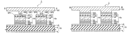
- the semiconductor device 1 includes: a mounting substrate 70 ; semiconductor chips 10 1 and 10 2 disposed on the mounting substrate 70 , the respective semiconductor chips 10 1 and 10 2 having a semiconductor substrate 26 , source pad electrodes SP 1 and SP 2 and gate pad electrodes GP 1 and GP 2 disposed on a surface of the semiconductor substrate 26 , and a drain pad electrode 36 disposed in contact with the mounting substrate 70 on a back side surface of the semiconductor substrate 26 ; and a source connector SC disposed on the source pad electrodes SP 1 and SP 2 .
- the mounting substrate 70 and the drain pad electrode 36 are bonded by using solid phase diffusion bonding.
- the semiconductor device 1 may further include a heat spreader 100 for mounting the mounting substrate 70 .
- the mounting substrate 70 and the heat spreader 100 are also bonded by using the solid phase diffusion bonding.
- the source pad electrodes SP 1 and SP 2 and the source connector SC are also bonded by using the solid phase diffusion bonding.
- the semiconductor device 1 may further include a gate connector GC disposed on the gate pad electrodes GP 1 and GP 2 .
- the gate pad electrodes GP 1 and GP 2 and the gate connector GC are bonded by using the solid phase diffusion bonding.
- the semiconductor device 1 may also include a plurality of the semiconductor chips 10 1 and 10 2 .
- the source connector SC may be simultaneously bonded to the respective source pad electrodes SP 1 and SP 2 of the semiconductor chips 10 1 and 10 2 by using the solid phase diffusion bonding.
- the gate connector GC may be simultaneously bonded to the respective gate pad electrodes GP 1 and GP 2 of the semiconductor chips 10 1 and 10 2 by using the solid phase diffusion bonding.
- the mounting substrate 70 may include an insulating substrate 8 and a metal layer 14 disposed on a surface of the insulating substrate 8 .
- a drain solid phase diffusion bonding layer 48 D between the metal layer 14 and the drain pad electrode 36 may be also provided between the mounting substrate 70 and the drain pad electrode 36 .
- the semiconductor device 1 may also include a source solid phase diffusion bonding layer 48 S formed between the source pad electrodes SP 1 and SP 2 and the source connector SC by using the solid phase diffusion bonding.
- the semiconductor device 1 may also include a gate solid phase diffusion bonding layer 48 G formed between the gate pad electrodes GP 1 and GP 2 and the gate connector GC by using the solid phase diffusion bonding.
- the mounting substrate 70 may include the insulating substrate 8 and a metal layer 6 disposed on a back side surface of the insulating substrate 8 , and a heat spreader solid phase diffusion bonding layer 48 H formed by using the solid phase diffusion bonding may be also provided between the mounting substrate 70 and the heat spreader 100 .
- the gate solid phase diffusion bonding layer 48 G, the source solid phase diffusion bonding layer 48 S, the drain solid phase diffusion bonding layer 48 D, and the heat spreader solid phase diffusion bonding layer 48 H can be formed by bonding one or more kinds of metals selected from the group consisting of Ag, Au, Ti and Ni, using the solid phase diffusion bonding process.
- one or more kinds of metals selected from the group consisting of Ag, Au, Ti and Ni can be formed by using plating technology, sputtering technology, or vacuum evaporation technology.
- the source connector SC and the gate connector GC can be formed with one material selected from the group consisting of aluminum (Al), copper (Cu), a copper molybdenum (CuMo) alloy, a copper tungsten (CuW) alloy, and Al—SiC.
- a value of the pressure applied to the respective bonding parts is not less than about 1 MPa but not more than about 100 MPa; and the heating processing temperature is not less than about 200 degrees C. but not more than about 350 degrees C.
- a fabrication method for the semiconductor device 1 includes: forming the drain solid phase diffusion bonding layer 48 D by bonding the mounting substrate 70 and the drain pad electrode 36 using the solid phase diffusion bonding; and forming the source solid phase diffusion bonding layer 48 S by bonding the source connector SC and the source pad electrodes SP 1 and SP 2 using the solid phase diffusion bonding.
- the step of forming the drain solid phase diffusion bonding layer 48 D and the step of forming the source solid phase diffusion bonding layer 48 S may be performed simultaneously.
- the fabrication method for the semiconductor device 1 may further include forming the heat spreader solid phase diffusion bonding layer 48 H by bonding the mounting substrate 70 and the heat spreader 100 for mounting the mounting substrate 70 using the solid phase diffusion bonding.
- the fabrication method for the semiconductor device 1 may further include forming the gate solid phase diffusion bonding layer 48 G by bonding the gate pad electrodes GP 1 and GP 2 and the gate connector GC disposed on the gate pad electrodes GP 1 and GP 2 using the solid phase diffusion bonding.
- a value of the pressure required for forming the solid phase diffusion bonding is not less than about 1 MPa but not more than about 100 MPa, for example; and the heating processing temperature required for forming the solid phase diffusion bonding is not less than about 200 degrees C. but not more than about 350 degrees C., for example.
- Ag, Au, Ti, Ni, etc. are formed on the drain side of the semiconductor chip 10 by using plating technology, sputtering technology, or vacuum evaporation technology.
- a structure of the drain pad electrode 36 in which Ti/Ni/Au/Ag are laminated one after another on the drain region 24 may be formed.
- an electrode structure in which Ni/Ag are laminated one after another may be formed on the above-mentioned Al.
- Ag, Au, Ti, Ni, etc. are formed on the insulating substrate 8 by using the plating technology, the sputtering technology, or the vacuum evaporation technology in order to form the mounting substrate 70 .
- the bonding is possible in any combination of the above-mentioned metals.
- bonding materials e.g., solder
- the interlayer metals 12 a and 12 b composed of solder (e.g., Ag) and/or the above-mentioned metal(s) may be disposed between the back side surface of the semiconductor chip 10 and the insulating substrate 8 in order to enhance the contact between the surfaces.
- the pressure is applied from both of the upper part of the semiconductor chip 10 and the lower part of the insulating substrate 8 .
- the value of the pressure is set to not less than about 1 MPa but not more than about 100 MPa, for example.
- the reason for applying the pressure is for enhancing the contact between the back side surface of the semiconductor chip 10 and the surface of the insulating substrate 8 .
- Plastic deformation occurs on the respective surfaces by increasing the applied the pressure during the process of making the contact, and thereby the contact surfaces will change the interface.
- heat as well as the pressure is also added.
- the heating processing temperature is set to about 200 degrees C. to about 350 degrees C. During the heating process, atomic diffusion creates in the newly formed interface at the bonded surface, thereby forming a clear bonded surface.
- the holding time period of the heating processing temperature (about 200 degrees C. to about 350 degrees C.) is approximately 20 minutes.
- the total cooling time period (heating processing temperature to room temperature) is approximately 20 minutes, whereas the heating time period from normal temperature to heating processing temperature is approximately 40 minutes. Therefore, the total process time period is within about 1 hour.
- Bonding between the insulating substrate 8 and a base plate can be formed similarly. That is, the metal layers 100 a and 100 b composed of Ag, Au, Ti, Ni, etc. are formed on the surface of the heat spreader 100 using the plating technology, the sputtering technology, or the vacuum evaporation technology. On the other hand, the metal layers 14 and 6 composed of Ag, Au, Ti, Ni, etc. are also formed on the surface of the insulating substrate 8 using the plating technology, the sputtering technology, or the vacuum evaporation technology.
- the back side surface of the insulating substrate 8 and the surface of the heat spreader 100 are contacted, and pressure and heat are applied in the same manner as mentioned above, thereby forming the heat spreader solid phase diffusion bonding layer 48 H.
- the surface of the drain pad electrode 36 of the semiconductor chip 10 and the surface of the mounting substrate 70 may be contacted, pressure and heat may be applied in the same manner as mentioned above, and thereby the drain solid phase diffusion bonding layer 48 D may be formed as well.
- the source solid phase diffusion bonding layer 48 S may be formed between the source connector SC and the source pad electrode SP, and the gate solid phase diffusion bonding layer 48 G may be also formed between the gate pad electrode GP and the gate connector GC.
- the order of forming the solid phase diffusion bonding layer is not limited in the above-mentioned order (i.e., the heat spreader solid phase diffusion bonding layer 48 H—the drain solid phase diffusion bonding layer 48 D—the source solid phase diffusion bonding layer 48 S—the gate solid phase diffusion bonding layer 48 G), but suitable order can be selected.
- the drain solid phase diffusion bonding layer 48 D, the source solid phase diffusion bonding layer 48 S and the gate solid phase diffusion bonding layer 48 G may be formed by simultaneous processes, and, finally the heat spreader solid phase diffusion bonding layer 48 H may be formed.
- source connector SC and the gate connector GC for being bonded to the source pad electrode SP and the gate pad electrode GP are prepared.
- Materials having high electrical conductivity and high thermal conductivity are fundamentally selected, and materials having a coefficient of thermal expansion near that of the semiconductor chip 10 to be mounted are also selected, as materials of the source connector SC and the gate connector GC.
- materials having high electrical conductivity and high thermal conductivity are also selected, as materials of the source connector SC and the gate connector GC.
- materials e.g., Al and Cu
- the source connector SC and gate connector GC can be also bonded simultaneously to a plurality of the semiconductor chips 10 .
- metal layers SM and GM composed of Ag, Au, Ti, Ni, etc. are formed on the surface of the semiconductor chip 10 (i.e., on the source pad electrode SP and the gate pad electrode GP) using plating technology, sputtering technology, or vacuum evaporation technology.
- Materials of the metal layers SM and GM can be changed depending on the materials of the source connector SC and the gate connector GC to be bonded thereto.
- the source connector SC and the gate connector GC are covered with a Ag plating layer
- the source pad electrode SP and the gate pad electrode GP of the semiconductor chip 10 are formed with Al, it is effective to apply Ni plating onto the source connector SC and the gate connector GC, in order to inhibit oxidation of Al. Since Al is an extremely soft metal, plastic deformation occurs easily under the solid phase diffusion bonding process. However, a state in a minimum amount of an oxide film is achieved by applying the Ni plating onto the source connector SC and the gate connector GC, and thereby the solid phase diffusion bonding can be formed easily.
- a configuration of the semiconductor device 1 according to the embodiment after the fabricating process thereof is represented as shown in FIG. 3 to FIG. 6 .
- the drain solid phase diffusion bonding layer 48 D is formed between the drain pad electrode 36 and the insulating substrate 8 of the semiconductor chip 10
- the gate solid phase diffusion bonding layer 48 G is also formed between the gate connector GC and the gate pad electrodes GP 1 and GP 2 of the semiconductor chip 10 .
- the drain solid phase diffusion bonding layer 48 D is formed between the drain pad electrode 36 and the insulating substrate 8 of the semiconductor chip 10
- the source solid phase diffusion bonding layer 48 S is also formed between the source connector SC and the source pad electrodes SP 1 and SP 2 of the semiconductor chip 10 .
- the surface of the drain pad electrode 36 is formed of Ag and the Ag plating is applied on the surface of the mounting substrate 70 , for example, by using the drain solid phase diffusion bonding process between the drain pad electrode 36 and the mounting substrate 70 of the semiconductor chip 10 , and thereby the solid phase diffusion bonding layer 48 D is formed by Ag—Ag bonding.
- a melting temperature of the solid phase diffusion bonding layer 48 D is also about 960 degrees C. which is a melting point of Ag.
- the solid phase diffusion bonding layers 48 D, 48 S, 48 H and 48 G having the high melting point can be obtained by the heating process at relatively low temperatures (about 200 degrees C. to about 350 degrees C.).
- the source pad electrode SP and the gate pad electrode GP is bonded, respectively, to the source connector SC and the gate connector GC by using the solid phase diffusion bonding, and the drain pad electrode 36 is bonded to the mounting substrate 70 by using the solid phase diffusion bonding, thereby achieving a wirebondless interconnection scheme and double-sided cooling method for the semiconductor chip 10 .
- the double-sided cooling performance of the semiconductor chip 10 can be further enhanced by bonding the mounting substrate 70 to the heat spreader 100 using the aforementioned solid phase diffusion bonding process.
- a schematic cross-sectional structure of the SiC-MOSFET includes: a semiconductor substrate 26 composed of an n-type high resistivity layer; P type base regions 28 formed in a surface side of the semiconductor substrate 26 ; source regions 30 formed in the surface of the p type base regions 28 ; a gate insulating film 32 disposed on the surface of the semiconductor substrate 26 between the p type base regions 28 ; a gate electrode 38 disposed on the gate insulating film 32 ; source electrodes 34 connected to the source regions 30 ; a n+ type drain region 24 disposed on a back side opposite to the surface of the semiconductor substrate 26 ; and a drain pad electrode 36 connected to the n+ type drain region 24 .
- the semiconductor chip 10 is composed of a planar-gate-type n channel vertical SiC-MOSFET, the semiconductor chip 10 may be composed of a trench-gate-type n channel vertical SiC-MOSFET etc.
- a GaN based FET etc. instead of the SiC-MOSFET are also applicable to the semiconductor chip 10 applied to the semiconductor device 1 according to the embodiment.
- One of an SiC based power device, a GaN based power device or an AlN based power device is applicable to the semiconductor chip 10 applied to the semiconductor device 1 according to the embodiment.
- a semiconductor whose bandgap energy is 1.1 eV to 8 eV, for example, can be also used for the semiconductor chip 10 applied to the semiconductor device 1 according to the embodiment.
- the solid phase diffusion bonding layers 48 G, 48 S, 48 D and 48 H have high heat resistance (e.g., the melting point of metallic silver reaches to about 960 degrees C.)
- the power device e.g., SiC based FET and a GaN based FET
- the solid phase diffusion bonding layers 48 G, 48 S, 48 D and 48 H can be driven at high temperature by applying the solid phase diffusion bonding layers 48 G, 48 S, 48 D and 48 H to the power device.
- FIG. 8 shows an example of the semiconductor module 10 applied to the semiconductor device 1 according to the embodiment, and is a schematic cross-sectional configuration diagram showing the SiC-MOSFET including a source pad electrode SP and a gate pad electrode GP.
- the gate pad electrode GP is connected to the gate electrode 38 disposed on the gate insulating film 32
- the source pad electrode SP is connected to the source electrode 34 connected to the source region 30 .
- the gate pad electrode GP and the source pad electrode SP are disposed on the interlayer insulating film 44 for passivation which covers the surface of the semiconductor chip 10 .
- a minuscule transistor structure may be formed in the semiconductor substrate 26 under the gate pad electrode GP and the source pad electrode SP, in the same manner as that of FIG. 7 or the central part of FIG. 8 .
- the source pad electrode SP may be disposed to extend onto the interlayer insulating film 44 for passivation, also in the transistor structure of the central part.
- the gate pad electrode GP may be disposed to extend onto the interlayer insulating film 44 for passivation, in the transistor structure of the central part of FIG. 8 .
- AC alternating current
- the three-phase AC inverter includes: a gate drive unit 50 , a power module unit 52 connected to the gate drive unit 50 , and a three-phase Alternating Current (AC) motor unit 54 .
- Inverters of U phase, V phase and W phase are connected to the power module unit 52 corresponding to U phase, V phase, and W phase of the three-phase AC motor unit 54 .
- SiC-MOSFETs Q 1 and Q 2 , Q 3 and Q 4 , and Q 5 and Q 6 having inverter configurations are connected between a positive terminal (+) and a negative terminal ( ⁇ ) to in which the capacitor C is connected. Furthermore, diodes D 1 to D 6 are connected inversely in parallel between the source and the drain of SiC-MOSFETs Q 1 to Q 6 , respectively.
- the SiC-MOSFETs Q 1 to Q 6 equivalent to the semiconductor chip 10 applied to the semiconductor device 1 according to the embodiment are electrically connected on the mounting substrate 70 or the heat spreader 100 via the solid phase diffusion bonding layers 48 G, 48 S, 48 D and 48 H.
- An actual solid phase diffusion bonding process is performed, after forming GC, Ag, Au, Ti, Ni, etc. on the surface of the materials of the source connector SC and the gate connector by using the plating technology, the sputtering technology, or the vacuum evaporation technology, and forming Ag, Au, Ti, Ni, etc. on the surface of source pad electrode SP and the gate pad electrode GP of the semiconductor chip 10 by using plating technology, sputtering technology, or vacuum evaporation technology.
- high pressure e.g., about 10 MPa to about 100 MPa
- heat e.g., about 200 degrees C. to about 350 degrees C.
- plastic deformation is caused by the pressure applied in order to contact surfaces of two materials to be bonded, and then atomic diffusion is further caused by the heat added thereto, thereby bonding the two materials.
- bonding between the drain pad electrode 36 and the insulating substrate 8 is also achievable by the above-mentioned solid phase diffusion bonding process.
- the pressure is from an upper part of the source connector SC and the gate connector GC, and also applied from a lower part of the insulating substrate 8 .
- the heat is further added at the same time, and thereby the solid phase diffusion bonding process is performed.
- FIG. 10A is a diagram for explaining a solid phase diffusion bonding process applied to the fabrication method for the semiconductor device 1 according to the embodiment, and is a schematic cross-sectional configuration diagram showing an aspect that two metallic materials M 1 and M 2 are opposed mutually.
- FIG. 10B is a schematic cross-sectional configuration diagram showing an aspect that the two metallic materials M 1 and M 2 are contacted to be opposed mutually and their contact interface BF becomes plastic-deformed under the high pressure.
- FIG. 10C is a schematic cross-sectional configuration diagram showing an aspect that the contact interface BF disappears completely and only one interface surface BS is formed.
- FIG. 10D is a schematic cross-sectional configuration diagram showing an aspect that the interface surface BS is removed by atomic diffusion and seamless solid phase diffusion bonding is formed.
- FIG. 11A is a diagram for explaining a drain solid phase diffusion bonding process applied to the fabrication method for the semiconductor device 1 according to the embodiment, and is a schematic bird's-eye view configuration diagram showing an upper member 56 used for applying the pressure from an upper side to the semiconductor chips 10 1 and 10 2 .
- FIG. 11B is a schematic bird's-eye view configuration diagram showing the semiconductor chips 10 1 and 10 2 and the interlayer metals 12 a and 12 b .
- FIG. 11C is a schematic bird's-eye view configuration diagram showing an intermediate member 60 used for inserting the semiconductor chips 10 1 and 10 2 and the interlayer metals 12 a and 12 b .
- FIG. 11A is a diagram for explaining a drain solid phase diffusion bonding process applied to the fabrication method for the semiconductor device 1 according to the embodiment, and is a schematic bird's-eye view configuration diagram showing an upper member 56 used for applying the pressure from an upper side to the semiconductor chips 10 1 and 10 2 .
- FIG. 11B is a schematic bird's-eye view
- FIG. 11D is a schematic bird's-eye view configuration diagram showing the mounting substrate 70 used for mounting the semiconductor chips 10 1 and 10 2 and the interlayer metals 12 a and 12 b .
- FIG. 11E is a schematic bird's-eye view configuration diagram showing a lower member 80 used for inserting the mounting substrates 70 and applying the pressure from an under side to the semiconductor chips 10 1 and 10 2 .
- FIG. 12A is a schematic planar pattern configuration diagram observing the upper member 56 of FIG. 11A from a back side surface thereof.
- FIG. 12B is a schematic planar pattern configuration diagram observing the intermediate member 60 of FIG. 11C from a surface thereof.
- FIG. 13 is a schematic cross-sectional configuration diagram for explaining an aspect that the configuration of FIG. 11 is assembled and then the pressure/heating process is subjected thereto, in the fabrication method for the semiconductor device 1 according to the embodiment.
- the interlayer metals 12 a and 12 b are omitted in FIG. 13 .
- the upper member 56 includes convex regions 56 a and 56 b for applying the pressure from an upper side to the semiconductor chips 10 1 and 10 2 , as shown in FIGS. 11A, 12A and 13 .
- the intermediate member 60 includes openings 60 a and 60 b for inserting the semiconductor chips 10 1 and 10 2 and the interlayer metals 12 a and 12 b , as shown in FIGS. 11C and 12B .
- the interlayer metals 12 a and 12 b are not necessarily required. However, when the surface of the mounting substrate 70 is rough, the interlayer metals 12 a and 12 b are useful in view of the fact that the contact between the surface of the drain pad electrode 36 and the surface of the mounting substrate 70 should be enhanced, and the formation of the drain solid phase diffusion bonding layer should be enhanced.
- the interlayer metals 12 a and 12 b can be formed of solder, such as Ag, or a platy member of Ag, Au, Ti, Ni, etc.
- FIG. 14 shows an example of a temperature profile and an example of a pressure profile under the drain solid phase diffusion bonding process.
- the pressure of about 90 MPa is applied in an initial state. Then, while this pressure is held, the heating processing temperature is risen from room temperature to 350 degrees C. within about 5 minutes. Next, the pressure of about 90 MPa and the heating processing temperature at about 350 degrees C. are held during about 20 minutes. Next, during about 25 minutes, the pressure is reduced from about 90 MPa to atmospheric pressure, and the heating processing temperature is reduced from about 350 degrees C. to about 200 degrees C. Next, during about 25 minutes, the heating processing temperature is reduced from about 200 degrees C. to room temperature. As clearly shown in FIG. 14 , since the pressure/heating process is completed within about 1 hour, shortening of the process time can be achieved by optimizing the aforementioned process.
- a schematic cross-sectional configuration of the mounting substrate 70 applied to the semiconductor device according to the embodiment may include metal layers 14 and 6 formed on the surface and the back side surface of the insulating substrate 8 . Since a low roughness substrate surface is required in order to form the drain solid phase diffusion bond, semiconductor substrates 7 (e.g., a silicon wafer) are also applicable instead of the mounting substrate 70 , as shown in FIG. 16 . In the example of FIG. 16 , a metal layer 5 is formed on the semiconductor substrate 7 .
- the metal layers 14 , 6 , and 5 can be formed of Ag, Au, Ti, Ni, etc. using the plating technology, the sputtering technology, or the vacuum evaporation technology.
- FIG. 17 shows an example of forward current-voltage characteristics in ON state of the semiconductor device according to the embodiment.
- a plurality of curves in FIG. 17 corresponds to a plurality of lots.
- FIG. 17 in the semiconductor device according to the embodiment 1, almost equivalent forward current-voltage characteristics are obtained over the plurality of the lots.
- same grade bonding as a conventional Pb solder bonding or high intensity bonding rather than the conventional Pb solder bonding is obtained under the room temperature or under the environment of 300 degrees C.
- FIG. 18 shows an example of a temperature profile under a thermal cycle test subjected to the semiconductor device 1 according to the embodiment.
- the thermal cycle test was performed over a range from ⁇ 50 degrees C. to +250 degrees C. under a nitrogen atmosphere.
- a time period of one heat cycle is 80 minutes.
- the breakdown of one heat cycle is as follows: a time period at a temperature of ⁇ 50 degrees C. is 30 minutes; a heating time period at a temperature from ⁇ 50 degrees C. to +250 degrees C. is 10 minutes; a time period at a temperature of +250 degrees C. is 30 minutes; and the cooling time period at a temperature from +250 degrees C. to ⁇ 50 degrees C. is 10 minutes.
- Characteristic degradation is not observed as a result of measuring the value of the forward voltage drop Vf and the value of the reverse breakdown voltage Vr every 100 cycles. As a result of measuring the value of the on resistance at the time of 70 cycles, substantial characteristic degradation is not also observed as compared with the value of the on resistance at the time of 0 cycles.
- Bonding strength of the solid phase diffusion bonding layers 48 S, 48 G, 48 D and 48 H formed by using the fabrication method of the semiconductor device according to the embodiment 1 is sufficiently secured as a result of the above thermal cycle test.
- FIG. 19A is a diagram for explaining a source solid phase diffusion bonding process applied to the fabrication method for the semiconductor device 1 according to the embodiment, and is a schematic bird's-eye view configuration diagram showing a source connector SC used for applying pressure from an upper side to the semiconductor chips 10 1 and 10 2 .
- FIG. 19B shows a schematic bird's-eye view structure of the semiconductor chips 10 1 and 10 2 and the interlayer metals 12 a and 12 b .
- FIG. 19C is a schematic bird's-eye view configuration diagram showing the intermediate member 60 used for inserting the semiconductor chips 10 1 and 10 2 and the interlayer metals 12 a and 12 b .
- FIG. 19A is a diagram for explaining a source solid phase diffusion bonding process applied to the fabrication method for the semiconductor device 1 according to the embodiment, and is a schematic bird's-eye view configuration diagram showing a source connector SC used for applying pressure from an upper side to the semiconductor chips 10 1 and 10 2 .
- FIG. 19B shows a schematic bird's-eye view structure
- FIG. 19D shows a schematic bird's-eye view structure of the semiconductor substrate 7 for mounting the semiconductor chips 10 1 and 10 2 and the interlayer metals 12 a and 12 b .
- FIG. 19E is a schematic bird's-eye view configuration diagram showing a lower member 80 used for inserting the semiconductor substrate 7 and applying the pressure from an under side to the semiconductor chips 10 1 and 10 2 .
- the interlayer metals 12 a and 12 b are not necessarily required. However, when the surface of the semiconductor substrate 7 is rough, the interlayer metals 12 a and 12 b are useful, in view of the fact that the contact between the surface of the drain pad electrode 36 and the surface of the semiconductor substrate 7 should be enhanced, and the formation of the drain solid phase diffusion bonding layer should be enhanced.
- the interlayer metals 12 a and 12 b can be formed of solder, such as Ag, or a platy member of Ag, Au, Ti, Ni, etc.
- the mounting substrate 70 may be also used in the same manner as shown in FIG. 11 .
- the similar example of the profile as shown in FIG. 14 can be also applied as an example of the temperature profile and an example of the pressure profile, in the source solid phase diffusion bonding process between the source pad electrode SP and the source connector SC, and the gate solid phase diffusion bonding process between the gate pad electrode GP and the gate connector GC, same as that of the drain solid phase diffusion bonding process.
- FIG. 20A shows an example of a photograph of the surface of the semiconductor device according to the embodiment formed by assembling the configuration of FIG. 19 and then subjecting the pressure/heating process thereto.
- FIG. 20B shows an example of a photograph of cross-sectional structure taken in the line V-V of FIG. 20A .
- the drain solid phase diffusion bonding layer 48 D is formed between the semiconductor substrate 7 and the drain pad electrode 36 at the same time of forming the source solid phase diffusion bonding layer 48 S between source connector SC and the source pad electrode SP.
- FIG. 21 shows an example of forward current-voltage characteristics in ON state of the semiconductor device 1 according to the embodiment in which the drain solid phase diffusion bonding layer 48 D is formed at the same time of forming the source solid phase diffusion bonding layer 48 S. It is confirmed that the characteristic degradation of the semiconductor chip 10 does not occur even when the source solid phase diffusion bonding layer 48 S and the drain solid phase diffusion bonding layer 48 D are simultaneously formed.
- the solid phase diffusion bonding layer is the melting point specific to Ag or Au
- the semiconductor chip can be driven at high temperature by applying the solid phase diffusion bonding layer to the SiC or GaN based power device etc.
- the semiconductor device since the electrical conductivity and thermal conductivity of the solid phase diffusion bonding layer are higher than those of the conventional low melting point solder, the semiconductor device having an enhanced electrical and thermal efficiency is achievable.
- the solid phase diffusion bonding layer having the high melting point can be formed under the low-temperature process, damage to the materials can be reduced at the time of the fabricating process.
- the diffusion bond process temperature and time is similar to a conventional high melting point Pb based solder, it can be mass produced using this packaging approach.
- the semiconductor device According to the semiconductor device according to the embodiment and the fabrication method for such semiconductor device, large capacity, mass production, shortening of process time, and simplification of processes are easily achievable, since the structure of disposing a plurality of the semiconductor chips in parallel can be also formed in a simultaneous processes.
- the present invention can provide the semiconductor device with double-sided cooling in which the process temperature and time can be reduced using the solid phase diffusion bonding process.
- the semiconductor device of a present invention can be used in general power devices (e.g., a power semiconductor module, an intelligent power module).
- general power devices e.g., a power semiconductor module, an intelligent power module.
Landscapes
- Engineering & Computer Science (AREA)
- Microelectronics & Electronic Packaging (AREA)
- Power Engineering (AREA)
- Computer Hardware Design (AREA)
- General Physics & Mathematics (AREA)
- Physics & Mathematics (AREA)
- Condensed Matter Physics & Semiconductors (AREA)
- Chemical & Material Sciences (AREA)
- Ceramic Engineering (AREA)
- Materials Engineering (AREA)
- Die Bonding (AREA)
- Cooling Or The Like Of Semiconductors Or Solid State Devices (AREA)
- Electrodes Of Semiconductors (AREA)
- Junction Field-Effect Transistors (AREA)
Abstract
Description
- Patent Literature 1: International publication No. WO 2006/074165
- Patent Literature 2: United States Patent Application Publication No. 2006/0151871
- Patent Literature 3: Japanese Patent Application Laying-Open Publication (Translation of PCT Application) No. H04-503480
- Patent Literature 4: Japanese Patent Application Laying-Open Publication No. 2010-245329
- Non Patent Literature 1: Warren C. Welch, III, Junseok Chae, and Khalil Najafi, “Transfer of Metal MEMS Packages Using a Wafer-Level Solder Transfer Technique”, IEEE TRANSACTION ON ADVANCED PACKAGING, VOL. 28, NO. 4, November 2005, pp. 643-649
- (a) First of all, as shown in
FIG. 10A , the two metallic materials M1 and M2 are opposed mutually to be adjacent to each other. - (b) Next, the two metallic materials M1 and M2 are opposed mutually to be contacted to each other, high pressure (e.g., not less than about 1 MPa but not more than about 100 MPa) is applied thereto, and thereby the contact interface BF is plastic-deformed, as shown in
FIG. 10B . - (c) Next, under the above-mentioned high pressure, when the heating process is performed, the contact interface BF disappears completely and then only one interface surface BS is formed, as shown in
FIG. 10C . The heating processing temperature at this time is not less than about 200 degrees C. but not more than about 350 degrees C., for example. - (d) When continuing the heating process under the above-mentioned high pressure, the interface surface BS of the two metallic materials M1 and M2 are removed by the atomic diffusion, and thereby forming a seamless solid phase diffusion bond, as shown in
FIG. 10D .
Claims (19)
Priority Applications (2)
| Application Number | Priority Date | Filing Date | Title |
|---|---|---|---|
| US13/403,341 US9761506B2 (en) | 2012-02-23 | 2012-02-23 | Semiconductor device and fabrication method for the same |
| JP2012093101A JP6006966B2 (en) | 2012-02-23 | 2012-04-16 | Semiconductor device and manufacturing method thereof |
Applications Claiming Priority (1)
| Application Number | Priority Date | Filing Date | Title |
|---|---|---|---|
| US13/403,341 US9761506B2 (en) | 2012-02-23 | 2012-02-23 | Semiconductor device and fabrication method for the same |
Publications (2)
| Publication Number | Publication Date |
|---|---|
| US20130221514A1 US20130221514A1 (en) | 2013-08-29 |
| US9761506B2 true US9761506B2 (en) | 2017-09-12 |
Family
ID=49001947
Family Applications (1)
| Application Number | Title | Priority Date | Filing Date |
|---|---|---|---|
| US13/403,341 Active 2032-04-05 US9761506B2 (en) | 2012-02-23 | 2012-02-23 | Semiconductor device and fabrication method for the same |
Country Status (2)
| Country | Link |
|---|---|
| US (1) | US9761506B2 (en) |
| JP (1) | JP6006966B2 (en) |
Families Citing this family (3)
| Publication number | Priority date | Publication date | Assignee | Title |
|---|---|---|---|---|
| WO2017094185A1 (en) * | 2015-12-04 | 2017-06-08 | ルネサスエレクトロニクス株式会社 | Semiconductor chip, semiconductor device, and electronic device |
| DE102015121775B3 (en) * | 2015-12-15 | 2016-12-15 | Infineon Technologies Ag | Method for connecting a semiconductor chip to a metallic surface of a substrate by means of two contact metallization layers and method for producing an electronic assembly |
| JP6685209B2 (en) * | 2016-09-12 | 2020-04-22 | 日立オートモティブシステムズ株式会社 | Semiconductor device |
Citations (15)
| Publication number | Priority date | Publication date | Assignee | Title |
|---|---|---|---|---|
| WO1990009255A1 (en) | 1989-02-14 | 1990-08-23 | Raychem Pontoise S.A. | Composite solder article |
| JPH04503480A (en) | 1989-02-14 | 1992-06-25 | レイケム・ソシエテ・アノニム | composite solder articles |
| US5421507A (en) * | 1990-06-11 | 1995-06-06 | International Business Machines Corporation | Au-Sn transient liquid bonding in high performance laminates |
| JPH09237868A (en) | 1996-02-29 | 1997-09-09 | Hitachi Ltd | Semiconductor module |
| JP2001110823A (en) | 1999-10-13 | 2001-04-20 | Hitachi Ltd | Manufacturing method of semiconductor device |
| JP2003082383A (en) | 2001-09-17 | 2003-03-19 | Kanebo Ltd | Perfume composition and cosmetic |
| JP2003092383A (en) | 2001-09-19 | 2003-03-28 | Hitachi Ltd | Power semiconductor device and its heat sink |
| JP2006500774A (en) | 2002-09-27 | 2006-01-05 | アーベーベー・リサーチ・リミテッド | Press pack power semiconductor module |
| US20060151871A1 (en) | 2005-01-07 | 2006-07-13 | Rockwell Scientific Licensing, Llc | High temperature, stable SiC device interconnects and packages having low thermal resistance |
| JP2008060529A (en) | 2006-08-29 | 2008-03-13 | Denso Corp | Power electronic package having two sheets of substrate mounting a plurality of electronic components |
| US20090290315A1 (en) * | 2006-07-20 | 2009-11-26 | Panasonic Corporation | Communication device and electronic apparatus using the same |
| JP2010245329A (en) | 2009-04-07 | 2010-10-28 | Toyota Motor Corp | Semiconductor device and method of manufacturing the same, and equipment using the same |
| US7847411B2 (en) * | 2003-11-07 | 2010-12-07 | Shinko Electric Industries Co., Ltd. | Electronic device and method of manufacturing the same |
| US20110254177A1 (en) * | 2006-08-29 | 2011-10-20 | Denso Corporation | Power electronic package having two substrates with multiple semiconductor chips and electronic components |
| US20130092948A1 (en) * | 2011-10-18 | 2013-04-18 | Rohm Co., Ltd. | Semiconductor device and fabrication method of the semiconductor device |
-
2012
- 2012-02-23 US US13/403,341 patent/US9761506B2/en active Active
- 2012-04-16 JP JP2012093101A patent/JP6006966B2/en active Active
Patent Citations (16)
| Publication number | Priority date | Publication date | Assignee | Title |
|---|---|---|---|---|
| JPH04503480A (en) | 1989-02-14 | 1992-06-25 | レイケム・ソシエテ・アノニム | composite solder articles |
| WO1990009255A1 (en) | 1989-02-14 | 1990-08-23 | Raychem Pontoise S.A. | Composite solder article |
| US5421507A (en) * | 1990-06-11 | 1995-06-06 | International Business Machines Corporation | Au-Sn transient liquid bonding in high performance laminates |
| JPH09237868A (en) | 1996-02-29 | 1997-09-09 | Hitachi Ltd | Semiconductor module |
| JP2001110823A (en) | 1999-10-13 | 2001-04-20 | Hitachi Ltd | Manufacturing method of semiconductor device |
| JP2003082383A (en) | 2001-09-17 | 2003-03-19 | Kanebo Ltd | Perfume composition and cosmetic |
| JP2003092383A (en) | 2001-09-19 | 2003-03-28 | Hitachi Ltd | Power semiconductor device and its heat sink |
| JP2006500774A (en) | 2002-09-27 | 2006-01-05 | アーベーベー・リサーチ・リミテッド | Press pack power semiconductor module |
| US7847411B2 (en) * | 2003-11-07 | 2010-12-07 | Shinko Electric Industries Co., Ltd. | Electronic device and method of manufacturing the same |
| US20060151871A1 (en) | 2005-01-07 | 2006-07-13 | Rockwell Scientific Licensing, Llc | High temperature, stable SiC device interconnects and packages having low thermal resistance |
| WO2006074165A2 (en) | 2005-01-07 | 2006-07-13 | Teledyne Licensing, Llc | HIGH TEMPERATURE, STABLE SiC DEVICE INTERCONNECTS AND PACKAGES HAVING LOW THERMAL RESISTANCE |
| US20090290315A1 (en) * | 2006-07-20 | 2009-11-26 | Panasonic Corporation | Communication device and electronic apparatus using the same |
| JP2008060529A (en) | 2006-08-29 | 2008-03-13 | Denso Corp | Power electronic package having two sheets of substrate mounting a plurality of electronic components |
| US20110254177A1 (en) * | 2006-08-29 | 2011-10-20 | Denso Corporation | Power electronic package having two substrates with multiple semiconductor chips and electronic components |
| JP2010245329A (en) | 2009-04-07 | 2010-10-28 | Toyota Motor Corp | Semiconductor device and method of manufacturing the same, and equipment using the same |
| US20130092948A1 (en) * | 2011-10-18 | 2013-04-18 | Rohm Co., Ltd. | Semiconductor device and fabrication method of the semiconductor device |
Non-Patent Citations (2)
| Title |
|---|
| Japanese Notification of Reasons for Refusal corresponding to Application No. 2012-093101; Date of Mailing: Mar. 15, 2016, with English translation. |
| Warren C. Welch, III et al., "Transfer of Metal MEMS Packages Using a Wafer-Level Solder Transfer Technique", IEE Transactions on Advanced Packaging, vol. 28, No. 4, Nov. 2005, pp. 643-649. |
Also Published As
| Publication number | Publication date |
|---|---|
| US20130221514A1 (en) | 2013-08-29 |
| JP2013175697A (en) | 2013-09-05 |
| JP6006966B2 (en) | 2016-10-12 |
Similar Documents
| Publication | Publication Date | Title |
|---|---|---|
| US9673163B2 (en) | Semiconductor device with flip chip structure and fabrication method of the semiconductor device | |
| US8513806B2 (en) | Laminated high melting point soldering layer formed by TLP bonding and fabrication method for the same, and semiconductor device | |
| US8592986B2 (en) | High melting point soldering layer alloyed by transient liquid phase and fabrication method for the same, and semiconductor device | |
| KR102585450B1 (en) | Molded package with chip carrier comprising brazed electrically conductive layers | |
| US8410590B2 (en) | Device including a power semiconductor chip electrically coupled to a leadframe via a metallic layer | |
| US8120153B1 (en) | High-temperature, wirebondless, injection-molded, ultra-compact hybrid power module | |
| CN111244041B (en) | Package comprising chip contact elements of two different conductive materials | |
| US8637379B2 (en) | Device including a semiconductor chip and a carrier and fabrication method | |
| US10475721B2 (en) | Power semiconductor device and method for manufacturing same | |
| JP7494271B2 (en) | Semiconductor device and power module | |
| US9324607B2 (en) | GaN power device with solderable back metal | |
| EP2541593A2 (en) | Laminated high melting point soldering layer and fabrication method for the same, and semiconductor device | |
| US20160315033A1 (en) | Device Including a Logic Semiconductor Chip Having a Contact Electrode for Clip Bonding | |
| CN104851843A (en) | Power semiconductor device | |
| US9761506B2 (en) | Semiconductor device and fabrication method for the same | |
| CN109075159B (en) | Semiconductor device and method for manufacturing the same | |
| CN109478543B (en) | Semiconductor device with a plurality of semiconductor chips | |
| JP2014053403A (en) | Power module semiconductor device | |
| JP2014032985A (en) | Semiconductor device and method for manufacturing the same | |
| JPH10223835A (en) | Semiconductor device and its manufacture | |
| JP2007150342A (en) | Semiconductor device and its manufacturing method | |
| WO2017157486A1 (en) | Semiconductor device | |
| EP3699958A1 (en) | Electronic chip reliably mounted with compressive strain | |
| Barlow et al. | High-temperature high-power packaging techniques for HEV traction applications | |
| KR20230092516A (en) | Double-sided heat dissipation power semiconductor module and its manufacturing method |
Legal Events
| Date | Code | Title | Description |
|---|---|---|---|
| AS | Assignment |
Owner name: ROHM CO., LTD., JAPAN Free format text: ASSIGNMENT OF ASSIGNORS INTEREST;ASSIGNORS:OTSUKA, TAKUKAZU;WESTERN, BRYON;PASSMORE, BRANDON;AND OTHERS;REEL/FRAME:028090/0248 Effective date: 20120419 Owner name: ARKANSAS POWER ELECTRONICS INTERNATIONAL, INC., AR Free format text: ASSIGNMENT OF ASSIGNORS INTEREST;ASSIGNORS:OTSUKA, TAKUKAZU;WESTERN, BRYON;PASSMORE, BRANDON;AND OTHERS;REEL/FRAME:028090/0248 Effective date: 20120419 |
|
| AS | Assignment |
Owner name: CREE FAYETTEVILLE, INC., ARKANSAS Free format text: MERGER;ASSIGNOR:ARKANSA POWER ELECTRONICS INTERNATIONAL, INC.;REEL/FRAME:037949/0210 Effective date: 20150708 |
|
| STCF | Information on status: patent grant |
Free format text: PATENTED CASE |
|
| MAFP | Maintenance fee payment |
Free format text: PAYMENT OF MAINTENANCE FEE, 4TH YEAR, LARGE ENTITY (ORIGINAL EVENT CODE: M1551); ENTITY STATUS OF PATENT OWNER: LARGE ENTITY Year of fee payment: 4 |
|
| AS | Assignment |
Owner name: CREE, INC., NORTH CAROLINA Free format text: MERGER;ASSIGNOR:CREE FAYETTEVILLE, INC.;REEL/FRAME:057291/0406 Effective date: 20210624 |
|
| AS | Assignment |
Owner name: WOLFSPEED, INC., NORTH CAROLINA Free format text: CHANGE OF NAME;ASSIGNOR:CREE, INC.;REEL/FRAME:059085/0667 Effective date: 20211004 |
|
| AS | Assignment |
Owner name: U.S. BANK TRUST COMPANY, NATIONAL ASSOCIATION, NORTH CAROLINA Free format text: SECURITY INTEREST;ASSIGNOR:WOLFSPEED, INC.;REEL/FRAME:064185/0755 Effective date: 20230623 |