EP3375136B1 - Ethernet-bus, steuergerät und verfahren zum aufwecken eines steuergeräts eines ethernet-busses - Google Patents
Ethernet-bus, steuergerät und verfahren zum aufwecken eines steuergeräts eines ethernet-busses Download PDFInfo
- Publication number
- EP3375136B1 EP3375136B1 EP16791541.2A EP16791541A EP3375136B1 EP 3375136 B1 EP3375136 B1 EP 3375136B1 EP 16791541 A EP16791541 A EP 16791541A EP 3375136 B1 EP3375136 B1 EP 3375136B1
- Authority
- EP
- European Patent Office
- Prior art keywords
- voltage
- control device
- center tap
- wake
- bus
- Prior art date
- Legal status (The legal status is an assumption and is not a legal conclusion. Google has not performed a legal analysis and makes no representation as to the accuracy of the status listed.)
- Active
Links
Images
Classifications
-
- H—ELECTRICITY
- H04—ELECTRIC COMMUNICATION TECHNIQUE
- H04L—TRANSMISSION OF DIGITAL INFORMATION, e.g. TELEGRAPHIC COMMUNICATION
- H04L12/00—Data switching networks
- H04L12/28—Data switching networks characterised by path configuration, e.g. LAN [Local Area Networks] or WAN [Wide Area Networks]
- H04L12/40—Bus networks
- H04L12/40006—Architecture of a communication node
- H04L12/40039—Details regarding the setting of the power status of a node according to activity on the bus
-
- G—PHYSICS
- G06—COMPUTING OR CALCULATING; COUNTING
- G06F—ELECTRIC DIGITAL DATA PROCESSING
- G06F13/00—Interconnection of, or transfer of information or other signals between, memories, input/output devices or central processing units
- G06F13/38—Information transfer, e.g. on bus
- G06F13/40—Bus structure
- G06F13/4063—Device-to-bus coupling
- G06F13/4068—Electrical coupling
-
- G—PHYSICS
- G06—COMPUTING OR CALCULATING; COUNTING
- G06F—ELECTRIC DIGITAL DATA PROCESSING
- G06F1/00—Details not covered by groups G06F3/00 - G06F13/00 and G06F21/00
- G06F1/26—Power supply means, e.g. regulation thereof
- G06F1/32—Means for saving power
- G06F1/3203—Power management, i.e. event-based initiation of a power-saving mode
- G06F1/3234—Power saving characterised by the action undertaken
- G06F1/3296—Power saving characterised by the action undertaken by lowering the supply or operating voltage
-
- H—ELECTRICITY
- H04—ELECTRIC COMMUNICATION TECHNIQUE
- H04L—TRANSMISSION OF DIGITAL INFORMATION, e.g. TELEGRAPHIC COMMUNICATION
- H04L12/00—Data switching networks
- H04L12/02—Details
- H04L12/12—Arrangements for remote connection or disconnection of substations or of equipment thereof
-
- H—ELECTRICITY
- H04—ELECTRIC COMMUNICATION TECHNIQUE
- H04L—TRANSMISSION OF DIGITAL INFORMATION, e.g. TELEGRAPHIC COMMUNICATION
- H04L12/00—Data switching networks
- H04L12/28—Data switching networks characterised by path configuration, e.g. LAN [Local Area Networks] or WAN [Wide Area Networks]
- H04L12/40—Bus networks
- H04L12/40006—Architecture of a communication node
- H04L12/40013—Details regarding a bus controller
-
- H—ELECTRICITY
- H04—ELECTRIC COMMUNICATION TECHNIQUE
- H04L—TRANSMISSION OF DIGITAL INFORMATION, e.g. TELEGRAPHIC COMMUNICATION
- H04L12/00—Data switching networks
- H04L12/28—Data switching networks characterised by path configuration, e.g. LAN [Local Area Networks] or WAN [Wide Area Networks]
- H04L12/40—Bus networks
- H04L2012/40267—Bus for use in transportation systems
- H04L2012/40273—Bus for use in transportation systems the transportation system being a vehicle
-
- Y—GENERAL TAGGING OF NEW TECHNOLOGICAL DEVELOPMENTS; GENERAL TAGGING OF CROSS-SECTIONAL TECHNOLOGIES SPANNING OVER SEVERAL SECTIONS OF THE IPC; TECHNICAL SUBJECTS COVERED BY FORMER USPC CROSS-REFERENCE ART COLLECTIONS [XRACs] AND DIGESTS
- Y02—TECHNOLOGIES OR APPLICATIONS FOR MITIGATION OR ADAPTATION AGAINST CLIMATE CHANGE
- Y02D—CLIMATE CHANGE MITIGATION TECHNOLOGIES IN INFORMATION AND COMMUNICATION TECHNOLOGIES [ICT], I.E. INFORMATION AND COMMUNICATION TECHNOLOGIES AIMING AT THE REDUCTION OF THEIR OWN ENERGY USE
- Y02D30/00—Reducing energy consumption in communication networks
- Y02D30/50—Reducing energy consumption in communication networks in wire-line communication networks, e.g. low power modes or reduced link rate
Definitions
- the invention relates to an Ethernet bus, a control device and a method for waking up a control device of an Ethernet bus.
- Control devices in a bus system should preferably only be active if their function is required. Otherwise, they should be deactivated and have no appreciable energy requirement.
- CAN and FlexRay special wake-up bus drivers are specified, which turn on a voltage regulator of a control unit as soon as a valid signal is on the bus.
- Ethernet bus systems no such standard exists so far.
- a wake-up signal as a differential signal on both data or bus lines.
- This may be an AC signal that is the same as the regular communication signal or a DC voltage.
- the circuits for impressing and for detecting the wake-up signal can adversely affect the symmetry and thus the transmission properties.
- US 2009/077394 describes a managed power system with a communications subsystem and a computing subsystem.
- the communication subsystem includes a network state module that determines communication power state information and transmits a power management message with the communication power state information.
- the system may further include a power management module for receiving the power management message, retrieving the communication power state information from the power management message, and managing power states for the computing subsystem based on the communication power state information.
- the invention is based on the technical problem of providing an Ethernet bus and a control unit, by means of which a control unit can be woken up without influencing the symmetry, as well as a method for waking up a control unit of an Ethernet bus.
- the Ethernet bus includes at least two controllers.
- a control unit can also be a switch.
- the control devices each have a bus driver and a microprocessor, wherein at least one first control device has a voltage regulator, which can set at least two voltage values for the operating voltage of the control unit. In this case, a first voltage value for an operating state "sleeping" or deactivated and the second voltage value for a operating state "communication” or “awake” or activated is provided.
- the bus drivers are connected to each other via at least two bus lines. On the bus lines in each case a termination network is connected, which is part of the respective control unit.
- the termination network has at least two resistors and a capacitor, wherein the two resistors are each connected to a bus line and are connected to one another at a center tap of the termination network, the capacitor of the termination network being arranged between center tap and ground.
- the Ethernet bus has at least one wake-up module, which is designed such that a voltage signal is generated in response to a wake-up event in order to change the voltage at the center tap of the control unit with the voltage regulator.
- the circuit is assigned to the at least one voltage regulator, by means of which the voltage regulator is controlled in dependence on the voltage at the center tap from the first voltage value to the second voltage value and thus woken up or activated. The symmetry of the data transfer is not affected.
- the voltage at the output of the wake-up module must be present only for a predetermined time and then can be switched off again, the voltage regulator remains set to the second voltage value, or the voltage at the output of the wake-up module is permanently on, as long the controller should remain active.
- the second control device also has a voltage regulator with two voltage values to which a circuit is assigned in order to evaluate the voltage at the center tap for the voltage regulator.
- the second control unit can also be deactivated, this being woken up automatically by waking up the first control unit, since a change in the voltage at the center tap of the first control unit via the bus leads also to a change in the voltage at the center tap of the other control unit.
- the second control device also has a wake-up module.
- the wake-up module and / or the circuit is integrated in the control unit.
- the circuit comprises a resistor and a transistor forming a voltage divider, wherein a control input of the voltage regulator is connected to a center tap of the voltage part, wherein the voltage divider between an operating voltage and ground, wherein a control input of the transistor with the center tap the termination network is connected.
- the wake-up module can turn on the transistor, which leads to a change in the voltage at the center tap of the voltage part and thus to switch the voltage regulator, It should be noted that a reverse logic is possible that, for example, the voltage of the wake-up module locks the transistor.
- the operating voltage at the circuit must not be equal to the operating voltage of the control unit.
- At least one filter is assigned to the wake-up module in order to suppress high-frequency common-mode interference.
- a throttle or a low-pass filter is arranged at the output of the wake-up module for this purpose. This will prevent these common mode noise from inadvertently waking up the controller.
- a low-pass filter can also be arranged at the input of the wake-up module in order to suppress input interference.
- a preferred field of application is the use in a motor vehicle.
- the invention will be explained in more detail below with reference to a preferred embodiment.
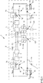
- the single figure shows a schematic block diagram of part of an Ethernet bus.
- FIG. 1 an Ethernet bus 1 with a first control unit 2 and a second control unit 3 is shown.
- the control devices 2, 3 each have a bus driver 4 and a microprocessor 5, wherein the bus drivers 4 are interconnected by at least two bus lines 6, 7.
- the two control devices 2, 3 each have a termination network 8, consisting of two resistors R1, R2 and a capacitor C3.
- the resistor R1 is connected to the bus line 6 and the resistor R2 to the bus line 7, wherein the two resistors are connected to one another at a center tap 9 of the termination network 8. Between the center tap 9 and ground, the capacitor C3 is arranged.
- the coupling capacitors C1, C2 of the second control unit 3 are not shown.
- the control units 2, 3 each have a voltage regulator 10, which converts a first operating voltage V BAT into an operating voltage V CC for the control unit 2, 3. In this case, this operating voltage V CC can be switched off (first voltage value) or switched on (second voltage value).
- the voltage regulator 10 is associated with a circuit 11 having a resistor R and a transistor T, which are connected in series between the operating voltage V BAT and ground.
- the circuit 11 forms a voltage divider, wherein the center tap 12 is connected to a control input 13 of the voltage regulator 10.
- a control input 14 of the transistor T is connected to the center tap 9 of the termination network 8
- the control units 2, 3 each have a wake-up module 15, which converts the operating voltage V BAT to an output voltage which is applied via a throttle L at the center tap 9.
- the recording module 15 has a control input 16 which switches through the output voltage as a function of a wake-up event S, whereby a low-pass filter 17 can still be arranged in front of the control input 16.
- the transistor T In the deactivated state, the transistor T is blocked, so that approximately V BAT is applied to the control input 13 of the voltage regulator 10. If now the control unit 2 are woken up, then a signal S is applied to the control input 16, whereby the output voltage of the wake-up module 15 is applied to the center tap 9 and raises its potential. As a result, the control input 14 controls the transistor T. As a result, the operating voltage V BAT drops via the resistor R and the control input 13 is pulled to ground. This causes the switching on of the operating voltage V CC for the microprocessor 5 and bus driver 4 (second voltage value). The increase of the potential at the center tap 9 of the control unit 2 is transmitted via the bus lines 6, 7 to the center tap 9 of the second control unit 3, so that there analog voltage regulator 10 is turned on.
Landscapes
- Engineering & Computer Science (AREA)
- Theoretical Computer Science (AREA)
- Signal Processing (AREA)
- Computer Networks & Wireless Communication (AREA)
- General Engineering & Computer Science (AREA)
- Physics & Mathematics (AREA)
- General Physics & Mathematics (AREA)
- Computer Hardware Design (AREA)
- Small-Scale Networks (AREA)
- Direct Current Feeding And Distribution (AREA)
- Semiconductor Integrated Circuits (AREA)
- Dc Digital Transmission (AREA)
- Power Sources (AREA)
Applications Claiming Priority (2)
| Application Number | Priority Date | Filing Date | Title |
|---|---|---|---|
| DE102015222112.1A DE102015222112A1 (de) | 2015-11-10 | 2015-11-10 | Ethernet-Bus, Steuergerät und Verfahren zum Aufwecken eines Steuergeräts eines Ethernet-Busses |
| PCT/EP2016/075380 WO2017080792A1 (de) | 2015-11-10 | 2016-10-21 | Ethernet-bus, steuergerät und verfahren zum aufwecken eines steuergeräts eines ethernet-busses |
Publications (2)
| Publication Number | Publication Date |
|---|---|
| EP3375136A1 EP3375136A1 (de) | 2018-09-19 |
| EP3375136B1 true EP3375136B1 (de) | 2019-06-26 |
Family
ID=57249777
Family Applications (1)
| Application Number | Title | Priority Date | Filing Date |
|---|---|---|---|
| EP16791541.2A Active EP3375136B1 (de) | 2015-11-10 | 2016-10-21 | Ethernet-bus, steuergerät und verfahren zum aufwecken eines steuergeräts eines ethernet-busses |
Country Status (7)
| Country | Link |
|---|---|
| US (1) | US10700887B2 (enExample) |
| EP (1) | EP3375136B1 (enExample) |
| JP (1) | JP6509435B2 (enExample) |
| KR (1) | KR101947972B1 (enExample) |
| CN (1) | CN108352993B (enExample) |
| DE (1) | DE102015222112A1 (enExample) |
| WO (1) | WO2017080792A1 (enExample) |
Families Citing this family (3)
| Publication number | Priority date | Publication date | Assignee | Title |
|---|---|---|---|---|
| WO2020122280A1 (ko) * | 2018-12-13 | 2020-06-18 | 엘지전자 주식회사 | 차량용 시스템 및 방법 |
| CN111490918B (zh) * | 2019-01-29 | 2021-07-30 | 广州汽车集团股份有限公司 | 车载以太网网络唤醒系统、方法、装置和计算机设备 |
| CN113993196B (zh) * | 2021-10-25 | 2024-01-30 | 浙江吉利控股集团有限公司 | 一种车载以太网的节点控制方法、系统、设备及存储介质 |
Family Cites Families (21)
| Publication number | Priority date | Publication date | Assignee | Title |
|---|---|---|---|---|
| DE19611945C1 (de) * | 1996-03-26 | 1997-11-20 | Daimler Benz Ag | Einrichtung für den busvernetzten Betrieb eines elektronischen Gerätes mit Microcontroller sowie deren Verwendung |
| JP2003143044A (ja) * | 2001-10-31 | 2003-05-16 | Matsushita Electric Ind Co Ltd | 2線式電源多重通信システム、そのマスター装置及び2線式電源多重通信方法 |
| US6747498B1 (en) * | 2002-12-20 | 2004-06-08 | Texas Instruments Incorporated | CAN receiver wake-up circuit |
| DE10358584A1 (de) * | 2002-12-30 | 2004-07-15 | Robert Bosch Gmbh | Verfahren und Vorrichtung zum Aufwecken von Teilnehmern eines Bussystems und entsprechender Teilnehmer |
| US7779451B2 (en) | 2006-03-30 | 2010-08-17 | Intel Corporation | Securing wakeup network events |
| US8156353B2 (en) | 2007-09-17 | 2012-04-10 | Intel Corporation | Techniques for communications power management based on system states |
| DE102008002946B4 (de) * | 2008-07-16 | 2010-04-08 | Lear Corporation Gmbh | Verfahren zum Detektieren eines Fehlers auf einer Datenleitung |
| CN101482734B (zh) * | 2009-01-22 | 2011-11-30 | 深圳市博孚机电有限公司 | 一种低功耗控制电路及低功耗控制电路的工作方法 |
| DE102009015197A1 (de) | 2009-03-31 | 2010-10-14 | Volkswagen Ag | Steuergerät für ein Fahrzeugnetzwerk und Verfahren zum Betreiben eines Fahrzeugnetzwerkes |
| EP2309677B1 (en) * | 2009-10-06 | 2012-09-05 | Nxp B.V. | Wake up detector for a bus transceiver |
| EP2339790A1 (en) * | 2009-12-28 | 2011-06-29 | Nxp B.V. | Definition of wakeup bus messages for partial networking |
| DE102010049835A1 (de) * | 2010-10-27 | 2012-05-03 | Volkswagen Ag | Netzwerk und Verfahren zum Betreiben eines Netzwerks |
| CN101977162B (zh) | 2010-12-03 | 2012-01-18 | 电子科技大学 | 一种高速网络的负载均衡方法 |
| US8578222B2 (en) * | 2011-02-17 | 2013-11-05 | Qualcomm Incorporated | SerDes power throttling as a function of detected error rate |
| US8862921B1 (en) * | 2011-12-02 | 2014-10-14 | Maxim Integrated Products, Inc. | Apparatus for remote wake-up during dedicated charging mode |
| KR101327077B1 (ko) * | 2011-12-15 | 2013-11-07 | 이날파 루프 시스템즈 그룹 비.브이. | 차량용 파노라마 선루프의 슬라이딩 구조 |
| CN103580969B (zh) * | 2012-07-19 | 2018-08-31 | 杭州三花研究院有限公司 | 一种lin网络从节点控制系统及方法 |
| DE102013004737A1 (de) * | 2013-03-19 | 2013-10-31 | Daimler Ag | Netzwerk und Verfahren zum Betrieb eines Netzwerks |
| DE102013208004B3 (de) * | 2013-05-02 | 2014-07-10 | Continental Automotive Gmbh | Weckschaltung für eine an einem Zweidrahtbus für ein differentielles Signal betreibbare Buskomponente und Buskomponente mit einer solchen Weckschaltung |
| WO2016147902A1 (ja) * | 2015-03-18 | 2016-09-22 | ソニー株式会社 | 送信装置、通信システム、及び、送信方法 |
| CN204659637U (zh) | 2015-05-26 | 2015-09-23 | 华域汽车电动系统有限公司 | 基于tja1041at接口芯片的整车can唤醒电路 |
-
2015
- 2015-11-10 DE DE102015222112.1A patent/DE102015222112A1/de not_active Withdrawn
-
2016
- 2016-10-21 WO PCT/EP2016/075380 patent/WO2017080792A1/de not_active Ceased
- 2016-10-21 JP JP2018516781A patent/JP6509435B2/ja active Active
- 2016-10-21 US US15/746,948 patent/US10700887B2/en active Active
- 2016-10-21 KR KR1020187004387A patent/KR101947972B1/ko active Active
- 2016-10-21 EP EP16791541.2A patent/EP3375136B1/de active Active
- 2016-10-21 CN CN201680065665.8A patent/CN108352993B/zh active Active
Non-Patent Citations (1)
| Title |
|---|
| None * |
Also Published As
| Publication number | Publication date |
|---|---|
| KR101947972B1 (ko) | 2019-02-13 |
| JP2018535588A (ja) | 2018-11-29 |
| US10700887B2 (en) | 2020-06-30 |
| EP3375136A1 (de) | 2018-09-19 |
| CN108352993B (zh) | 2020-11-24 |
| JP6509435B2 (ja) | 2019-05-08 |
| US20180241583A1 (en) | 2018-08-23 |
| DE102015222112A1 (de) | 2017-05-11 |
| WO2017080792A1 (de) | 2017-05-18 |
| CN108352993A (zh) | 2018-07-31 |
| KR20180030137A (ko) | 2018-03-21 |
Similar Documents
| Publication | Publication Date | Title |
|---|---|---|
| EP0588274B1 (de) | Serielles Bus-System mit einer Eindrahtverbindung | |
| EP3766216B1 (de) | Sende-/empfangseinrichtung für ein bussystem und betriebsverfahren hierfür | |
| EP3375149A1 (de) | Einrichtung und verfahren zum selektiven ausblenden von busschwingungen beim datenempfang über ein bussystem | |
| DE102015121732A1 (de) | Schaltungsanordnung für einen schaltbaren Leitungsabschluss eines seriellen Busses | |
| DE102014118156A1 (de) | Bus-Treiberschaltung mit verbesserter Übergangsgeschwindigkeit | |
| EP3375136B1 (de) | Ethernet-bus, steuergerät und verfahren zum aufwecken eines steuergeräts eines ethernet-busses | |
| DE102009041434A1 (de) | Verfahren und Vorrichtung zum Aufwecken von Teilnehmern eines Bussystems und entsprechender Teilnehmer | |
| WO2012055525A1 (de) | Netzwerk und verfahren zum betreiben eines netzwerks | |
| DE10223773B4 (de) | Schaltungsanordnung und Verfahren zur Überwachung eines Mikrocontrollers | |
| DE4342036C2 (de) | Datenbussystem | |
| DE10335905A1 (de) | Verfahren und Vorrichtung zur bidirektionalen Eindraht-Datenübertragung | |
| DE102008053534B3 (de) | Sklavenschaltung eines LIN-Busses und Verfahren zum Betrieb | |
| DE102020110984A1 (de) | Bus-transceiver | |
| DE102013220707B4 (de) | Verfahren zum Betreiben eines Datenbusses, entsprechender Datenbus und Fahrzeug mit einem solchen Datenbus | |
| DE102011007849A1 (de) | Steuergerät mit digitaler Schnittstelle | |
| EP1240054B1 (de) | Schaltungsanordnung zur aktivierung eines can-bus-steuergerätes | |
| DE102006023274B4 (de) | Verfahren und Vorrichtung zum Steuern von Netzwerksegmenten eines Netzwerks in einem Kraftfahrzeug | |
| WO2017076572A1 (de) | Bussystem und verfahren zur diagnose eines kurzschlusses | |
| WO2019242906A1 (de) | I3c-slave-schnittstelle, integrierte schaltung mit einer i3c-slave-schnittstelle und verfahren zum betreiben einer i3c-slave-schnittstelle | |
| WO2012055526A1 (de) | Netzwerk und verfahren zum betreiben eines netzwerks | |
| DE3937814A1 (de) | Verfahren zur uebertragung von daten sowie anordnung | |
| EP3665874B1 (de) | Sende-/empfangseinrichtung für ein bussystem und verfahren zur reduzierung einer schwingneigung beim übergang zwischen unterschiedlichen bitzuständen | |
| EP0332097A2 (de) | Datenbus für Kraftfahrzeuge | |
| DE10011775A1 (de) | Schaltungsanordnung zur Aktivierung eines CAN-Bus-Steuergerätes | |
| DE102013208004B3 (de) | Weckschaltung für eine an einem Zweidrahtbus für ein differentielles Signal betreibbare Buskomponente und Buskomponente mit einer solchen Weckschaltung |
Legal Events
| Date | Code | Title | Description |
|---|---|---|---|
| STAA | Information on the status of an ep patent application or granted ep patent |
Free format text: STATUS: UNKNOWN |
|
| STAA | Information on the status of an ep patent application or granted ep patent |
Free format text: STATUS: THE INTERNATIONAL PUBLICATION HAS BEEN MADE |
|
| PUAI | Public reference made under article 153(3) epc to a published international application that has entered the european phase |
Free format text: ORIGINAL CODE: 0009012 |
|
| STAA | Information on the status of an ep patent application or granted ep patent |
Free format text: STATUS: REQUEST FOR EXAMINATION WAS MADE |
|
| 17P | Request for examination filed |
Effective date: 20180611 |
|
| AK | Designated contracting states |
Kind code of ref document: A1 Designated state(s): AL AT BE BG CH CY CZ DE DK EE ES FI FR GB GR HR HU IE IS IT LI LT LU LV MC MK MT NL NO PL PT RO RS SE SI SK SM TR |
|
| AX | Request for extension of the european patent |
Extension state: BA ME |
|
| DAV | Request for validation of the european patent (deleted) | ||
| DAX | Request for extension of the european patent (deleted) | ||
| GRAP | Despatch of communication of intention to grant a patent |
Free format text: ORIGINAL CODE: EPIDOSNIGR1 |
|
| STAA | Information on the status of an ep patent application or granted ep patent |
Free format text: STATUS: GRANT OF PATENT IS INTENDED |
|
| INTG | Intention to grant announced |
Effective date: 20190329 |
|
| GRAS | Grant fee paid |
Free format text: ORIGINAL CODE: EPIDOSNIGR3 |
|
| GRAA | (expected) grant |
Free format text: ORIGINAL CODE: 0009210 |
|
| STAA | Information on the status of an ep patent application or granted ep patent |
Free format text: STATUS: THE PATENT HAS BEEN GRANTED |
|
| AK | Designated contracting states |
Kind code of ref document: B1 Designated state(s): AL AT BE BG CH CY CZ DE DK EE ES FI FR GB GR HR HU IE IS IT LI LT LU LV MC MK MT NL NO PL PT RO RS SE SI SK SM TR |
|
| REG | Reference to a national code |
Ref country code: GB Ref legal event code: FG4D Free format text: NOT ENGLISH |
|
| REG | Reference to a national code |
Ref country code: CH Ref legal event code: EP |
|
| REG | Reference to a national code |
Ref country code: DE Ref legal event code: R096 Ref document number: 502016005302 Country of ref document: DE |
|
| REG | Reference to a national code |
Ref country code: AT Ref legal event code: REF Ref document number: 1149578 Country of ref document: AT Kind code of ref document: T Effective date: 20190715 |
|
| REG | Reference to a national code |
Ref country code: IE Ref legal event code: FG4D Free format text: LANGUAGE OF EP DOCUMENT: GERMAN |
|
| REG | Reference to a national code |
Ref country code: NL Ref legal event code: MP Effective date: 20190626 |
|
| PG25 | Lapsed in a contracting state [announced via postgrant information from national office to epo] |
Ref country code: HR Free format text: LAPSE BECAUSE OF FAILURE TO SUBMIT A TRANSLATION OF THE DESCRIPTION OR TO PAY THE FEE WITHIN THE PRESCRIBED TIME-LIMIT Effective date: 20190626 Ref country code: LT Free format text: LAPSE BECAUSE OF FAILURE TO SUBMIT A TRANSLATION OF THE DESCRIPTION OR TO PAY THE FEE WITHIN THE PRESCRIBED TIME-LIMIT Effective date: 20190626 Ref country code: FI Free format text: LAPSE BECAUSE OF FAILURE TO SUBMIT A TRANSLATION OF THE DESCRIPTION OR TO PAY THE FEE WITHIN THE PRESCRIBED TIME-LIMIT Effective date: 20190626 Ref country code: AL Free format text: LAPSE BECAUSE OF FAILURE TO SUBMIT A TRANSLATION OF THE DESCRIPTION OR TO PAY THE FEE WITHIN THE PRESCRIBED TIME-LIMIT Effective date: 20190626 Ref country code: SE Free format text: LAPSE BECAUSE OF FAILURE TO SUBMIT A TRANSLATION OF THE DESCRIPTION OR TO PAY THE FEE WITHIN THE PRESCRIBED TIME-LIMIT Effective date: 20190626 Ref country code: NO Free format text: LAPSE BECAUSE OF FAILURE TO SUBMIT A TRANSLATION OF THE DESCRIPTION OR TO PAY THE FEE WITHIN THE PRESCRIBED TIME-LIMIT Effective date: 20190926 |
|
| REG | Reference to a national code |
Ref country code: LT Ref legal event code: MG4D |
|
| PG25 | Lapsed in a contracting state [announced via postgrant information from national office to epo] |
Ref country code: LV Free format text: LAPSE BECAUSE OF FAILURE TO SUBMIT A TRANSLATION OF THE DESCRIPTION OR TO PAY THE FEE WITHIN THE PRESCRIBED TIME-LIMIT Effective date: 20190626 Ref country code: GR Free format text: LAPSE BECAUSE OF FAILURE TO SUBMIT A TRANSLATION OF THE DESCRIPTION OR TO PAY THE FEE WITHIN THE PRESCRIBED TIME-LIMIT Effective date: 20190927 Ref country code: RS Free format text: LAPSE BECAUSE OF FAILURE TO SUBMIT A TRANSLATION OF THE DESCRIPTION OR TO PAY THE FEE WITHIN THE PRESCRIBED TIME-LIMIT Effective date: 20190626 Ref country code: BG Free format text: LAPSE BECAUSE OF FAILURE TO SUBMIT A TRANSLATION OF THE DESCRIPTION OR TO PAY THE FEE WITHIN THE PRESCRIBED TIME-LIMIT Effective date: 20190926 |
|
| PG25 | Lapsed in a contracting state [announced via postgrant information from national office to epo] |
Ref country code: PT Free format text: LAPSE BECAUSE OF FAILURE TO SUBMIT A TRANSLATION OF THE DESCRIPTION OR TO PAY THE FEE WITHIN THE PRESCRIBED TIME-LIMIT Effective date: 20191028 Ref country code: RO Free format text: LAPSE BECAUSE OF FAILURE TO SUBMIT A TRANSLATION OF THE DESCRIPTION OR TO PAY THE FEE WITHIN THE PRESCRIBED TIME-LIMIT Effective date: 20190626 Ref country code: CZ Free format text: LAPSE BECAUSE OF FAILURE TO SUBMIT A TRANSLATION OF THE DESCRIPTION OR TO PAY THE FEE WITHIN THE PRESCRIBED TIME-LIMIT Effective date: 20190626 Ref country code: NL Free format text: LAPSE BECAUSE OF FAILURE TO SUBMIT A TRANSLATION OF THE DESCRIPTION OR TO PAY THE FEE WITHIN THE PRESCRIBED TIME-LIMIT Effective date: 20190626 Ref country code: EE Free format text: LAPSE BECAUSE OF FAILURE TO SUBMIT A TRANSLATION OF THE DESCRIPTION OR TO PAY THE FEE WITHIN THE PRESCRIBED TIME-LIMIT Effective date: 20190626 Ref country code: SK Free format text: LAPSE BECAUSE OF FAILURE TO SUBMIT A TRANSLATION OF THE DESCRIPTION OR TO PAY THE FEE WITHIN THE PRESCRIBED TIME-LIMIT Effective date: 20190626 |
|
| PG25 | Lapsed in a contracting state [announced via postgrant information from national office to epo] |
Ref country code: ES Free format text: LAPSE BECAUSE OF FAILURE TO SUBMIT A TRANSLATION OF THE DESCRIPTION OR TO PAY THE FEE WITHIN THE PRESCRIBED TIME-LIMIT Effective date: 20190626 Ref country code: IT Free format text: LAPSE BECAUSE OF FAILURE TO SUBMIT A TRANSLATION OF THE DESCRIPTION OR TO PAY THE FEE WITHIN THE PRESCRIBED TIME-LIMIT Effective date: 20190626 Ref country code: SM Free format text: LAPSE BECAUSE OF FAILURE TO SUBMIT A TRANSLATION OF THE DESCRIPTION OR TO PAY THE FEE WITHIN THE PRESCRIBED TIME-LIMIT Effective date: 20190626 Ref country code: IS Free format text: LAPSE BECAUSE OF FAILURE TO SUBMIT A TRANSLATION OF THE DESCRIPTION OR TO PAY THE FEE WITHIN THE PRESCRIBED TIME-LIMIT Effective date: 20191026 |
|
| PG25 | Lapsed in a contracting state [announced via postgrant information from national office to epo] |
Ref country code: TR Free format text: LAPSE BECAUSE OF FAILURE TO SUBMIT A TRANSLATION OF THE DESCRIPTION OR TO PAY THE FEE WITHIN THE PRESCRIBED TIME-LIMIT Effective date: 20190626 |
|
| PG25 | Lapsed in a contracting state [announced via postgrant information from national office to epo] |
Ref country code: DK Free format text: LAPSE BECAUSE OF FAILURE TO SUBMIT A TRANSLATION OF THE DESCRIPTION OR TO PAY THE FEE WITHIN THE PRESCRIBED TIME-LIMIT Effective date: 20190626 Ref country code: PL Free format text: LAPSE BECAUSE OF FAILURE TO SUBMIT A TRANSLATION OF THE DESCRIPTION OR TO PAY THE FEE WITHIN THE PRESCRIBED TIME-LIMIT Effective date: 20190626 |
|
| PG25 | Lapsed in a contracting state [announced via postgrant information from national office to epo] |
Ref country code: IS Free format text: LAPSE BECAUSE OF FAILURE TO SUBMIT A TRANSLATION OF THE DESCRIPTION OR TO PAY THE FEE WITHIN THE PRESCRIBED TIME-LIMIT Effective date: 20200320 Ref country code: MC Free format text: LAPSE BECAUSE OF FAILURE TO SUBMIT A TRANSLATION OF THE DESCRIPTION OR TO PAY THE FEE WITHIN THE PRESCRIBED TIME-LIMIT Effective date: 20190626 |
|
| REG | Reference to a national code |
Ref country code: CH Ref legal event code: PL |
|
| REG | Reference to a national code |
Ref country code: DE Ref legal event code: R097 Ref document number: 502016005302 Country of ref document: DE |
|
| PLBE | No opposition filed within time limit |
Free format text: ORIGINAL CODE: 0009261 |
|
| STAA | Information on the status of an ep patent application or granted ep patent |
Free format text: STATUS: NO OPPOSITION FILED WITHIN TIME LIMIT |
|
| PG2D | Information on lapse in contracting state deleted |
Ref country code: IS |
|
| PG25 | Lapsed in a contracting state [announced via postgrant information from national office to epo] |
Ref country code: LU Free format text: LAPSE BECAUSE OF NON-PAYMENT OF DUE FEES Effective date: 20191021 Ref country code: CH Free format text: LAPSE BECAUSE OF NON-PAYMENT OF DUE FEES Effective date: 20191031 Ref country code: LI Free format text: LAPSE BECAUSE OF NON-PAYMENT OF DUE FEES Effective date: 20191031 |
|
| 26N | No opposition filed |
Effective date: 20200603 |
|
| REG | Reference to a national code |
Ref country code: BE Ref legal event code: MM Effective date: 20191031 |
|
| PG25 | Lapsed in a contracting state [announced via postgrant information from national office to epo] |
Ref country code: SI Free format text: LAPSE BECAUSE OF FAILURE TO SUBMIT A TRANSLATION OF THE DESCRIPTION OR TO PAY THE FEE WITHIN THE PRESCRIBED TIME-LIMIT Effective date: 20190626 Ref country code: BE Free format text: LAPSE BECAUSE OF NON-PAYMENT OF DUE FEES Effective date: 20191031 |
|
| PG25 | Lapsed in a contracting state [announced via postgrant information from national office to epo] |
Ref country code: IE Free format text: LAPSE BECAUSE OF NON-PAYMENT OF DUE FEES Effective date: 20191021 Ref country code: FR Free format text: LAPSE BECAUSE OF NON-PAYMENT OF DUE FEES Effective date: 20191031 |
|
| PG25 | Lapsed in a contracting state [announced via postgrant information from national office to epo] |
Ref country code: CY Free format text: LAPSE BECAUSE OF FAILURE TO SUBMIT A TRANSLATION OF THE DESCRIPTION OR TO PAY THE FEE WITHIN THE PRESCRIBED TIME-LIMIT Effective date: 20190626 |
|
| GBPC | Gb: european patent ceased through non-payment of renewal fee |
Effective date: 20201021 |
|
| PG25 | Lapsed in a contracting state [announced via postgrant information from national office to epo] |
Ref country code: MT Free format text: LAPSE BECAUSE OF FAILURE TO SUBMIT A TRANSLATION OF THE DESCRIPTION OR TO PAY THE FEE WITHIN THE PRESCRIBED TIME-LIMIT Effective date: 20190626 Ref country code: HU Free format text: LAPSE BECAUSE OF FAILURE TO SUBMIT A TRANSLATION OF THE DESCRIPTION OR TO PAY THE FEE WITHIN THE PRESCRIBED TIME-LIMIT; INVALID AB INITIO Effective date: 20161021 |
|
| PG25 | Lapsed in a contracting state [announced via postgrant information from national office to epo] |
Ref country code: GB Free format text: LAPSE BECAUSE OF NON-PAYMENT OF DUE FEES Effective date: 20201021 |
|
| PG25 | Lapsed in a contracting state [announced via postgrant information from national office to epo] |
Ref country code: MK Free format text: LAPSE BECAUSE OF FAILURE TO SUBMIT A TRANSLATION OF THE DESCRIPTION OR TO PAY THE FEE WITHIN THE PRESCRIBED TIME-LIMIT Effective date: 20190626 |
|
| REG | Reference to a national code |
Ref country code: AT Ref legal event code: MM01 Ref document number: 1149578 Country of ref document: AT Kind code of ref document: T Effective date: 20211021 |
|
| PG25 | Lapsed in a contracting state [announced via postgrant information from national office to epo] |
Ref country code: AT Free format text: LAPSE BECAUSE OF NON-PAYMENT OF DUE FEES Effective date: 20211021 |
|
| P01 | Opt-out of the competence of the unified patent court (upc) registered |
Effective date: 20230523 |
|
| PGFP | Annual fee paid to national office [announced via postgrant information from national office to epo] |
Ref country code: DE Payment date: 20251031 Year of fee payment: 10 |