EP3346247A1 - Sensor device - Google Patents
Sensor device Download PDFInfo
- Publication number
- EP3346247A1 EP3346247A1 EP16841346.6A EP16841346A EP3346247A1 EP 3346247 A1 EP3346247 A1 EP 3346247A1 EP 16841346 A EP16841346 A EP 16841346A EP 3346247 A1 EP3346247 A1 EP 3346247A1
- Authority
- EP
- European Patent Office
- Prior art keywords
- voltage
- sensor device
- operational amplifier
- resistance
- sensor
- Prior art date
- Legal status (The legal status is an assumption and is not a legal conclusion. Google has not performed a legal analysis and makes no representation as to the accuracy of the status listed.)
- Granted
Links
- 238000001514 detection method Methods 0.000 claims abstract description 28
- 239000003990 capacitor Substances 0.000 claims description 10
- 230000008520 organization Effects 0.000 claims description 3
- 230000000694 effects Effects 0.000 description 19
- 238000000034 method Methods 0.000 description 18
- 230000008569 process Effects 0.000 description 18
- 230000003321 amplification Effects 0.000 description 12
- 238000003199 nucleic acid amplification method Methods 0.000 description 12
- 230000036039 immunity Effects 0.000 description 10
- 238000010586 diagram Methods 0.000 description 6
- 230000003071 parasitic effect Effects 0.000 description 3
- 230000008859 change Effects 0.000 description 2
- 238000005259 measurement Methods 0.000 description 2
- 230000001133 acceleration Effects 0.000 description 1
- 238000006243 chemical reaction Methods 0.000 description 1
- 239000012530 fluid Substances 0.000 description 1
- 230000020169 heat generation Effects 0.000 description 1
- 230000009467 reduction Effects 0.000 description 1
- 239000004065 semiconductor Substances 0.000 description 1
- 238000005549 size reduction Methods 0.000 description 1
Images


Classifications
-
- B—PERFORMING OPERATIONS; TRANSPORTING
- B60—VEHICLES IN GENERAL
- B60R—VEHICLES, VEHICLE FITTINGS, OR VEHICLE PARTS, NOT OTHERWISE PROVIDED FOR
- B60R16/00—Electric or fluid circuits specially adapted for vehicles and not otherwise provided for; Arrangement of elements of electric or fluid circuits specially adapted for vehicles and not otherwise provided for
- B60R16/02—Electric or fluid circuits specially adapted for vehicles and not otherwise provided for; Arrangement of elements of electric or fluid circuits specially adapted for vehicles and not otherwise provided for electric constitutive elements
- B60R16/03—Electric or fluid circuits specially adapted for vehicles and not otherwise provided for; Arrangement of elements of electric or fluid circuits specially adapted for vehicles and not otherwise provided for electric constitutive elements for supply of electrical power to vehicle subsystems or for
-
- G—PHYSICS
- G01—MEASURING; TESTING
- G01D—MEASURING NOT SPECIALLY ADAPTED FOR A SPECIFIC VARIABLE; ARRANGEMENTS FOR MEASURING TWO OR MORE VARIABLES NOT COVERED IN A SINGLE OTHER SUBCLASS; TARIFF METERING APPARATUS; MEASURING OR TESTING NOT OTHERWISE PROVIDED FOR
- G01D21/00—Measuring or testing not otherwise provided for
-
- G—PHYSICS
- G01—MEASURING; TESTING
- G01D—MEASURING NOT SPECIALLY ADAPTED FOR A SPECIFIC VARIABLE; ARRANGEMENTS FOR MEASURING TWO OR MORE VARIABLES NOT COVERED IN A SINGLE OTHER SUBCLASS; TARIFF METERING APPARATUS; MEASURING OR TESTING NOT OTHERWISE PROVIDED FOR
- G01D3/00—Indicating or recording apparatus with provision for the special purposes referred to in the subgroups
- G01D3/08—Indicating or recording apparatus with provision for the special purposes referred to in the subgroups with provision for safeguarding the apparatus, e.g. against abnormal operation, against breakdown
-
- G—PHYSICS
- G01—MEASURING; TESTING
- G01D—MEASURING NOT SPECIALLY ADAPTED FOR A SPECIFIC VARIABLE; ARRANGEMENTS FOR MEASURING TWO OR MORE VARIABLES NOT COVERED IN A SINGLE OTHER SUBCLASS; TARIFF METERING APPARATUS; MEASURING OR TESTING NOT OTHERWISE PROVIDED FOR
- G01D5/00—Mechanical means for transferring the output of a sensing member; Means for converting the output of a sensing member to another variable where the form or nature of the sensing member does not constrain the means for converting; Transducers not specially adapted for a specific variable
- G01D5/12—Mechanical means for transferring the output of a sensing member; Means for converting the output of a sensing member to another variable where the form or nature of the sensing member does not constrain the means for converting; Transducers not specially adapted for a specific variable using electric or magnetic means
-
- G—PHYSICS
- G01—MEASURING; TESTING
- G01L—MEASURING FORCE, STRESS, TORQUE, WORK, MECHANICAL POWER, MECHANICAL EFFICIENCY, OR FLUID PRESSURE
- G01L9/00—Measuring steady of quasi-steady pressure of fluid or fluent solid material by electric or magnetic pressure-sensitive elements; Transmitting or indicating the displacement of mechanical pressure-sensitive elements, used to measure the steady or quasi-steady pressure of a fluid or fluent solid material, by electric or magnetic means
-
- G—PHYSICS
- G01—MEASURING; TESTING
- G01R—MEASURING ELECTRIC VARIABLES; MEASURING MAGNETIC VARIABLES
- G01R19/00—Arrangements for measuring currents or voltages or for indicating presence or sign thereof
- G01R19/165—Indicating that current or voltage is either above or below a predetermined value or within or outside a predetermined range of values
-
- G—PHYSICS
- G01—MEASURING; TESTING
- G01R—MEASURING ELECTRIC VARIABLES; MEASURING MAGNETIC VARIABLES
- G01R31/00—Arrangements for testing electric properties; Arrangements for locating electric faults; Arrangements for electrical testing characterised by what is being tested not provided for elsewhere
- G01R31/28—Testing of electronic circuits, e.g. by signal tracer
- G01R31/282—Testing of electronic circuits specially adapted for particular applications not provided for elsewhere
- G01R31/2829—Testing of circuits in sensor or actuator systems
-
- G—PHYSICS
- G05—CONTROLLING; REGULATING
- G05F—SYSTEMS FOR REGULATING ELECTRIC OR MAGNETIC VARIABLES
- G05F1/00—Automatic systems in which deviations of an electric quantity from one or more predetermined values are detected at the output of the system and fed back to a device within the system to restore the detected quantity to its predetermined value or values, i.e. retroactive systems
- G05F1/10—Regulating voltage or current
- G05F1/46—Regulating voltage or current wherein the variable actually regulated by the final control device is dc
- G05F1/462—Regulating voltage or current wherein the variable actually regulated by the final control device is dc as a function of the requirements of the load, e.g. delay, temperature, specific voltage/current characteristic
- G05F1/465—Internal voltage generators for integrated circuits, e.g. step down generators
-
- H—ELECTRICITY
- H03—ELECTRONIC CIRCUITRY
- H03K—PULSE TECHNIQUE
- H03K17/00—Electronic switching or gating, i.e. not by contact-making and –breaking
- H03K17/30—Modifications for providing a predetermined threshold before switching
-
- G—PHYSICS
- G01—MEASURING; TESTING
- G01D—MEASURING NOT SPECIALLY ADAPTED FOR A SPECIFIC VARIABLE; ARRANGEMENTS FOR MEASURING TWO OR MORE VARIABLES NOT COVERED IN A SINGLE OTHER SUBCLASS; TARIFF METERING APPARATUS; MEASURING OR TESTING NOT OTHERWISE PROVIDED FOR
- G01D5/00—Mechanical means for transferring the output of a sensing member; Means for converting the output of a sensing member to another variable where the form or nature of the sensing member does not constrain the means for converting; Transducers not specially adapted for a specific variable
- G01D5/12—Mechanical means for transferring the output of a sensing member; Means for converting the output of a sensing member to another variable where the form or nature of the sensing member does not constrain the means for converting; Transducers not specially adapted for a specific variable using electric or magnetic means
- G01D5/14—Mechanical means for transferring the output of a sensing member; Means for converting the output of a sensing member to another variable where the form or nature of the sensing member does not constrain the means for converting; Transducers not specially adapted for a specific variable using electric or magnetic means influencing the magnitude of a current or voltage
- G01D5/16—Mechanical means for transferring the output of a sensing member; Means for converting the output of a sensing member to another variable where the form or nature of the sensing member does not constrain the means for converting; Transducers not specially adapted for a specific variable using electric or magnetic means influencing the magnitude of a current or voltage by varying resistance
Definitions
- the present invention relates to an in-vehicle sensor device.
- a sensor device is driven by receiving power supply from an external control device, and the sensor device outputs, to the control device, a physical quantity of a fluid flowing in an intake pipe, such as a flow rate, as an analog voltage.
- a voltage amplitude range of this analog voltage is needed to be from substantially 0 V to a power voltage supplied from the control device. Additionally, often used is a voltage 5 V or 12 V as the power voltage supplied from the control device.
- a sensor device disclosed in PTL 1 uses power from a control device without any change as power for a signal processing circuit of the sensor device.
- a signal processing circuit provides higher performance by application of a microfabrication process.
- reduction of a drive voltage is demanded in order to prevent heat generation in the circuit, or the like.
- a signal output value to a control device is needed to be output within a range up to a voltage supplied from the control device.
- the present invention is made in view of the above-described situation and directed to providing a sensor device in which a voltage of a signal processing circuit can be lowered.
- a sensor device of the present invention includes a physical quantity detection unit, an output terminal, and an operational amplifier adapted to receive a detection signal of the physical quantity detection unit and output an output signal to the output terminal, in which the operational amplifier is driven with a voltage lower than the supplied voltage, and a negative organization signal having a voltage lower than the output signal is received.
- the present invention it is possible to provide a sensor device in which output amplitude can be obtained up to a power voltage by using a signal processing circuit that is operated with a low voltage equal to or lower than the power voltage of the sensor device.
- FIGS. 1 and 2 First, a sensor device according to a first practical example of the present invention will be described with reference to FIGS. 1 and 2 .
- a sensor device 1 of the present practical example is connected to a control device 10 via a power source line Vcc, a ground line Gnd, and a sensor output line Vout.
- the sensor device 1 has a power source terminal 7 connected to the power source line Vcc, a ground terminal 9 connected to the ground line Gnd, and a sensor output terminal 8 connected to the sensor output line Vout.
- the sensor device 1 is driven by power supplied from the control device 10 via the power source line Vcc and the ground line Gnd. Then, the sensor device 1 sends a sensor output voltage to the control device 10 from the sensor output terminal 8 via the sensor output line Vout.
- the control device 10 has: a constant voltage source 11 that supplies a constant voltage to the sensor device 1; and a pull-up resistor 12 connected between the sensor output line Vout and the constant voltage source 11.
- the sensor device 1 includes: a physical quantity detection unit 2 in which a voltage Vsen is changed in accordance with a measured physical quantity, a regulator 3 in which a power voltage supplied via the power source terminal 7 is received and a voltage lower than the power voltage is generated; an open collector type operational amplifier 4 that is operated with the low voltage supplied from the regulator 3 and controls a voltage of the sensor output terminal 8; and resistance elements 5 and 6 constituting a voltage divider that divides the voltage of the sensor output terminal 8.
- a pressure sensor, an acceleration sensor, an angular velocity sensor, an air flow rate sensor, or the like is used as the physical quantity detection unit 2.
- the sensor device 1 changes a voltage, namely, an output signal output from the sensor output terminal 8 in accordance with a measured physical quantity measured by the physical quantity detection unit 2.
- an output range of the sensor device 1 is a requested measurement range of a measured physical quantity and is needed to be changed from substantially 0 V to a voltage Vcc of the power source terminal 7.
- an output voltage Vreg supplied from the regulator 3 to the operational amplifier 4 is a voltage lower than a maximum voltage of the sensor output terminal 8. Therefore, the operational amplifier 4 is driven with the voltage Vreg that is lower than the maximum voltage of the sensor output terminal 8.
- the physical quantity detection unit 2 outputs an analog voltage Vsen in a range from 0 V to Vreg (output voltage of the regulator 3) in accordance with the measured physical quantity.
- This analog voltage Vsen is connected to a non-inversion input of the operational amplifier 4.
- the operational amplifier 4 controls an output MOS transistor to control the voltage of the sensor output terminal 8.
- the sensor output line Vout connected to the sensor output terminal 8 is connected to the power source line Vcc via the pull-up resistor 12. Therefore, the output voltage of the sensor output terminal 8 can be changed from 0 V to the voltage Vcc of the power source terminal 7 by changing ON resistance of the output MOS transistor of the operational amplifier 4.
- a resistance circuit formed of the resistors 5 and 6 is provided between the sensor output terminal 8 and an inversion input of the operational amplifier 4.
- the voltage of the sensor output terminal 8 divided by the resistance elements 5 and 6 is received in the inversion input of the operational amplifier 4, and negative feedback is applied to the operational amplifier 4.
- the output analog voltage Vsen of the physical quantity detection unit 2 is amplified with an amplification factor corresponding to a voltage division ratio determined by the resistance elements 5 and 6, and is output with a characteristic illustrated in FIG. 2 .
- the voltage Vreg that is a low voltage is supplied as power for the operational amplifier 4 as illustrated in FIG. 2 .
- an in-phase input range of the operational amplifier 4 is made lower than the voltage Vreg, and the negative feedback voltage determined by the resistance elements 5 and 6 is determined so as to fall within the in-phase input range of the operational amplifier 4.
- the negative feedback voltage generated by voltage division in the resistance circuit is made to fall within the in-phase input range of the operational amplifier 4.
- the voltage of the sensor output terminal 8 can be changed from 0 V to the voltage Vcc of the power source terminal 7 even in a case of using the operational amplifier 4 operated with the low-voltage power supplied from the regulator 3.
- a first effect is that a drive voltage of the operational amplifier 4 can be lowered.
- the operational amplifier 4 can be manufactured by a microfabrication process and can be miniaturized into a chip size. Additionally, since the high-performance MOS transistor can be used by application of the microfabrication process, the operational amplifier 4 can achieve higher performance. Furthermore, since the operational amplifier 4 can be manufactured by the microfabrication process, a large-scale logic circuit can be arranged on a same semiconductor chip as the operational amplifier 4. Therefore, the sensor device 1 can have complicated functions while being formed in a small area.
- a second effect is that an input circuit of the operational amplifier 4 having degraded noise immunity due to application of the microfabrication process can be easily protected.
- the sensor output terminal 8 is connected to the control device 10 via the sensor output line Vout, but the output line Vout is laid over a long distance, and external noise is applied to the output line Vout from a noise source existing around the output line Vout. Therefore, in a case where no countermeasure is taken in a state where the noise immunity is degraded due to application of the microfabrication process, a noise voltage is applied to the sensor output terminal 8 via the power source line, and the sensor device 1 may be destroyed.
- the sensor device 1 of the present practical example reduces such a noise voltage by the voltage divider (resistance circuit) formed of the resistance elements 5 and 6. Therefore, in the present practical example, there are effects in that noise current is reduced by resistance itself of the resistance element 5 and also the noise voltage is reduced by a time constant generated by resistance of the resistance element 5 and a parasitic capacitance existing in the resistance element 5. With the effects, the input circuit of the operational amplifier 4 having the degraded noise immunity due to application of the microfabrication process can be easily protected. Meanwhile, resistance values of the resistance elements 5 and 6 are preferably high, more preferably, 10 k ⁇ or more. Additionally, one end of the resistance element 6 is preferably connected to the ground in order to increase the effect of reducing the noise voltage by voltage division performed by the resistance elements 5 and 6.
- the open collector type has been described as the operational amplifier 4, but an open drain type may also be applicable.
- FIG. 3 illustrates a circuit configuration of the sensor device of the second practical example.
- the sensor device of the second practical example has a configuration basically same as that of the sensor device of the first practical example, but following improvements are added.
- protection performance for the input circuit of the operational amplifier 4 is improved by adding Zener diodes 13 and 14.
- the input circuit of the operational amplifier 4 is protected by the resistance elements 5 and 6 as described in the first practical example, but the noise immunity is further improved by adding the Zener diodes 13 and 14. Meanwhile, current flowing when noise is applied to the Zener diodes 13 and 14 is limited by the resistance elements 5 and 6, and therefore, size reduction can be achieved.
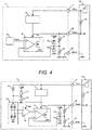
- FIG. 4 illustrates a circuit configuration of the sensor device of the third practical example.
- the sensor device of the third practical example has a configuration basically same as that of the sensor device of the first practical example, but following improvements are added.
- added are: a resistance type physical quantity detection element 16, a resistance element 15 connecting the power source terminal 7 to the physical quantity detection element 16; Zener diodes 17 and 18 connected to one end of the resistance element 15 and protecting the physical quantity detection element 16 from power source noise; and an amplifier 19 to amplify output voltage of the physical quantity detection element 16.
- power for the amplifier 19 is supplied from the output voltage Vreg of a regulator 3.
- a bridge circuit is formed with resistance elements in the resistance type physical quantity detection element 16, and an output voltage of the bridge circuit is changed when a resistance value is changed in accordance with a measured physical quantity.
- the ratiometric characteristic is the characteristic often used in an automotive sensor and the like.
- the power voltage of the internal signal processing circuit amplifier 19 and operational amplifier 4
- the ratiometric characteristic can be obtained.
- a first effect is that the power voltage of the internal signal processing circuit (amplifier 19 and operational amplification 4) can be lowered.
- the signal processing circuit (amplifier 19 and operational amplification 4) can be manufactured by the microfabrication process and can be miniaturized into a chip size. Additionally, since the high performance MOS transistor can be used by application of the microfabrication process, performance of the signal processing circuit (amplifier 19 and operational amplification 4) can be further improved.
- the signal processing circuit (amplifier 19 and operational amplification 4) can be manufactured by the microfabrication process, it is possible to arrange a large-scale logic circuit on a chip same as the signal processing circuit (amplifier 19 and operational amplification 4), and the sensor device 1 can have complicated functions.
- a second effect is that an input circuit of the amplifier 19 having degraded noise immunity due to application of the microfabrication process can be easily protected.
- the power source terminal 7 is connected to the control device 10 via the power source line Vcc, but external noise is applied to the output line Vcc due to the facts that the output line Vcc is laid over a long distance and a noise source exists around the output line Vcc, and a noise voltage is generated at the power source terminal 7 and the sensor device 1 may be destroyed.
- the noise voltage is reduced by voltage division performed by a voltage divider formed of the resistance element 15 and the physical quantity detecting element 16; noise current is reduced by resistance itself of the resistance element 15; and also the noise voltage is reduced by a time constant generated by resistance of the resistance element 15 and a parasitic capacitance existing in the resistance element 15.
- a resistance value of the resistance element 15 is preferably high, more preferably, 10 k ⁇ or more. Additionally, the noise immunity is further improved by adding the Zener diodes 17 and 18.
- a third effect is that a ratiometric characteristic can be obtained. Since the ratiometric characteristic can simplify an AD conversion circuit of the control device 10, this characteristic is often used in an automotive sensor.
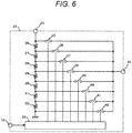
- FIG. 5 illustrates a circuit configuration of the sensor device of the fourth practical example
- FIG. 6 illustrates a circuit configuration of a DA converter 23.
- the sensor device of the fourth practical example has a configuration basically same as that of the sensor device of the first practical example, but following improvements are added.
- a signal from the physical quantity detection unit 2 is digitally processed by an arithmetic unit 24, the digital signal is converted into an analog signal by the resistance type DA converter 23, and a voltage of the sensor output terminal 8 is generated via an operational amplification 4.
- Zener diodes 20 and 21 to protect a resistance element 22 and the DA converter 23 from power source noise are added between the resistance type DA converter 23 and the power source terminal 7. Note that power for the DA converter 23 is supplied from the output voltage Vreg of the regulator 3.
- the DA converter 23 includes: a reference power source terminal 25; resistors 26, 27, 28, 29, 30, 31, and 32 connected between the reference power source terminal 25 and the ground; a digital input terminal 33 to receive a digital value from the arithmetic unit 24; a decoder 34 to decode a signal from the digital input terminal 33; and switches 35, 36, 37, 38, 39, 40, 41, and 42 controlled to be turned on/off by a signal from the decoder 34 and functioning to select respective connection points of the resistors 26, 27, 28, 29, 30, 31, and 32.
- the DA converter 23 is made to have a ratiometric characteristic by connecting the DA converter 23 to the power source terminal 7 via the resistance element 22. Furthermore, a voltage applied to the DA converter 23 is lowered by connecting the resistance element 22 to the DA converter 23 such that operation can be performed with the low-voltage power of the regulator 3 and also the voltage is made to fall within an input range of the operational amplifier 4 operated with the low-voltage power of the regulator 3.
- a first effect is that the power voltage of the internal signal processing circuit (arithmetic unit 24, DA converter 23, and operational amplification 4) can be lowered.
- the signal processing circuit can be manufactured by the microfabrication process and can be miniaturized into a chip size. Additionally, since the high performance MOS transistor can be used by application of microfabrication process, performance of the signal processing circuit can be further improved.
- a second effect is that the DA converter 23 having degraded noise immunity due to application of the microfabrication process can be easily protected. As described above, external noise is applied to the power source terminal 7 and may destroy the sensor device 1.
- the noise voltage is reduced by voltage division performed by a voltage divider formed of the resistance element 22 and the DA converter 23; noise current is reduced by resistance itself of the resistance element 22; and also the noise voltage is reduced by a time constant generated by resistance of the resistance element 22 and a parasitic capacitance existing in the resistance element 22.
- the DA converter 23 having the degraded noise immunity due to application of the microfabrication process can be easily protected.
- the noise immunity is further improved by adding the Zener diodes 20 and 21.
- a third effect is that a ratiometric characteristic can be obtained.
- FIG. 7 illustrates a circuit configuration of the sensor device of the fifth practical example.
- the sensor device of the fifth practical example has a configuration basically same as that of the sensor device of the fourth practical example, but following improvements are added.
- the operational amplifier 4 is used as inverting amplification. Therefore, a resistor 44 is disposed between an output of the DA converter 23 and the operational amplifier 4, a resistor 45 is disposed between an inversion input of the operational amplification 4 and a connection point for the resistance elements 5 and 6, resistance elements 46 and 47 are disposed between the ground and a connection point for the resistance element 22 and the DA converter 23, and a connection point for the resistance elements 46 and 47 is connected to a non-inversion input of the operational amplifier 4.
- the operational amplification 4 is used as an inverting amplifier. Therefore, voltage change at the inversion input and the non-inversion input of the operational amplifier 4 can be reduced.
- the power voltage of the operational amplifier 4 can be further lowered by using the operational amplifier 4 as the inverting amplifier, and further microfabrication process can be achieved.
- FIG. 8 illustrates a circuit configuration of the sensor device of the sixth practical example.
- the sensor device of the sixth practical example has a configuration basically same as that of the sensor device of the fifth practical example, but following improvements are added.
- resistance elements 44 and 45 are utilized in using the operational amplifier 4 as the inverting amplifier, but in the present practical example, a switched capacitor circuit is formed. Therefore, switches 48 and 50 and a capacitor 49 are disposed instead of the resistor 44, switches 51 and 53 and a capacitor 52 are disposed instead of the resistor 45, and a capacitor 54 is disposed between the inversion input of the operational amplification 4 and the sensor output terminal 8 in order to stabilize a system.
- non-linearity is generated in a characteristic of the sensor output terminal 8 by mutual influence between the resistance elements 5, 6, and 45.
- the resistor 45 is needed to be formed large enough for the resistors 5 and 6, but a resistance ratio inside an integrated circuit is limited.
- the switched capacitor circuit is used in the present practical example instead of the resistance elements.
- the switched capacitor circuit can easily form a high equivalent resistance. Therefore, in the present practical example, the non-linearity of the sensor output terminal 8 can be remarkably reduced.
Abstract
Description
- The present invention relates to an in-vehicle sensor device.
- As an example of an in-vehicle sensor device, there is a sensor device disclosed in
PTL 1. - According to
PTL 1, a sensor device is driven by receiving power supply from an external control device, and the sensor device outputs, to the control device, a physical quantity of a fluid flowing in an intake pipe, such as a flow rate, as an analog voltage. A voltage amplitude range of this analog voltage is needed to be from substantially 0 V to a power voltage supplied from the control device. Additionally, often used is a voltage 5 V or 12 V as the power voltage supplied from the control device. - PTL 1:
JP 2014-25731 A - A sensor device disclosed in
PTL 1 uses power from a control device without any change as power for a signal processing circuit of the sensor device. In recent years, a signal processing circuit provides higher performance by application of a microfabrication process. In a case of applying such a processing circuit, reduction of a drive voltage is demanded in order to prevent heat generation in the circuit, or the like. However, in an in-vehicle sensor device, a signal output value to a control device is needed to be output within a range up to a voltage supplied from the control device. InPTL 1, there still is room to examine such output within the range demanded as the sensor device while achieving a microfabrication process of the processing circuit. - The present invention is made in view of the above-described situation and directed to providing a sensor device in which a voltage of a signal processing circuit can be lowered.
- To solve the above problem, a sensor device of the present invention includes a physical quantity detection unit, an output terminal, and an operational amplifier adapted to receive a detection signal of the physical quantity detection unit and output an output signal to the output terminal, in which the operational amplifier is driven with a voltage lower than the supplied voltage, and a negative organization signal having a voltage lower than the output signal is received.
- According to the present invention, it is possible to provide a sensor device in which output amplitude can be obtained up to a power voltage by using a signal processing circuit that is operated with a low voltage equal to or lower than the power voltage of the sensor device.
-
- [
FIG. 1] FIG. 1 is a diagram illustrating a circuit configuration of a sensor device according to a first practical example. - [
FIG. 2] FIG. 2 is a graph illustrating a relation between a measured physical quantity and an output voltage Vout of asensor device 1. - [
FIG. 3] FIG. 3 is a diagram illustrating a circuit configuration of a sensor device according to a second practical example. - [
FIG. 4] FIG. 4 is a diagram illustrating a circuit configuration of a sensor device according to a third practical example. - [
FIG. 5] FIG. 5 is a diagram illustrating a circuit configuration of a sensor device according to a fourth practical example. - [
FIG. 6] FIG. 6 is a circuit configuration of aDA converter 23. - [
FIG. 7] FIG. 7 is a diagram illustrating a circuit configuration of a sensor device according to a fifth practical example. - [
FIG. 8] FIG. 8 is a diagram illustrating a circuit configuration of a sensor device according to a sixth practical example. - In the following, an embodiment of the present invention will be described with reference to the drawings.
- First, a sensor device according to a first practical example of the present invention will be described with reference to
FIGS. 1 and 2 . - A
sensor device 1 of the present practical example is connected to acontrol device 10 via a power source line Vcc, a ground line Gnd, and a sensor output line Vout. Thesensor device 1 has apower source terminal 7 connected to the power source line Vcc, aground terminal 9 connected to the ground line Gnd, and asensor output terminal 8 connected to the sensor output line Vout. Thesensor device 1 is driven by power supplied from thecontrol device 10 via the power source line Vcc and the ground line Gnd. Then, thesensor device 1 sends a sensor output voltage to thecontrol device 10 from thesensor output terminal 8 via the sensor output line Vout. Thecontrol device 10 has: aconstant voltage source 11 that supplies a constant voltage to thesensor device 1; and a pull-up resistor 12 connected between the sensor output line Vout and theconstant voltage source 11. Thesensor device 1 includes: a physical quantity detection unit 2 in which a voltage Vsen is changed in accordance with a measured physical quantity, aregulator 3 in which a power voltage supplied via thepower source terminal 7 is received and a voltage lower than the power voltage is generated; an open collector type operational amplifier 4 that is operated with the low voltage supplied from theregulator 3 and controls a voltage of thesensor output terminal 8; andresistance elements sensor output terminal 8. Note that a pressure sensor, an acceleration sensor, an angular velocity sensor, an air flow rate sensor, or the like is used as the physical quantity detection unit 2. - Next, an output signal of the
sensor device 1 and an output voltage of theregulator 3 will be described by usingFIG. 2 . Thesensor device 1 changes a voltage, namely, an output signal output from thesensor output terminal 8 in accordance with a measured physical quantity measured by the physical quantity detection unit 2. Here, an output range of thesensor device 1 is a requested measurement range of a measured physical quantity and is needed to be changed from substantially 0 V to a voltage Vcc of thepower source terminal 7. Additionally, an output voltage Vreg supplied from theregulator 3 to the operational amplifier 4 is a voltage lower than a maximum voltage of thesensor output terminal 8. Therefore, the operational amplifier 4 is driven with the voltage Vreg that is lower than the maximum voltage of thesensor output terminal 8. - Next, operation of the
sensor device 1 of the present practical example will be described. The physical quantity detection unit 2 outputs an analog voltage Vsen in a range from 0 V to Vreg (output voltage of the regulator 3) in accordance with the measured physical quantity. This analog voltage Vsen is connected to a non-inversion input of the operational amplifier 4. The operational amplifier 4 controls an output MOS transistor to control the voltage of thesensor output terminal 8. The sensor output line Vout connected to thesensor output terminal 8 is connected to the power source line Vcc via the pull-up resistor 12. Therefore, the output voltage of thesensor output terminal 8 can be changed from 0 V to the voltage Vcc of thepower source terminal 7 by changing ON resistance of the output MOS transistor of the operational amplifier 4. A resistance circuit formed of theresistors sensor output terminal 8 and an inversion input of the operational amplifier 4. The voltage of thesensor output terminal 8 divided by theresistance elements resistance elements FIG. 2 . At this point, the voltage Vreg that is a low voltage is supplied as power for the operational amplifier 4 as illustrated inFIG. 2 . Therefore, in the present practical example, an in-phase input range of the operational amplifier 4 is made lower than the voltage Vreg, and the negative feedback voltage determined by theresistance elements sensor output terminal 8 is changed from 0 V to the voltage Vcc, the negative feedback voltage generated by voltage division in the resistance circuit is made to fall within the in-phase input range of the operational amplifier 4. As a result, in thesensor device 1 of the present practical example, the voltage of thesensor output terminal 8 can be changed from 0 V to the voltage Vcc of thepower source terminal 7 even in a case of using the operational amplifier 4 operated with the low-voltage power supplied from theregulator 3. - Next, effects of the present practical example will be described. First of all, a first effect is that a drive voltage of the operational amplifier 4 can be lowered. As a result, the operational amplifier 4 can be manufactured by a microfabrication process and can be miniaturized into a chip size. Additionally, since the high-performance MOS transistor can be used by application of the microfabrication process, the operational amplifier 4 can achieve higher performance. Furthermore, since the operational amplifier 4 can be manufactured by the microfabrication process, a large-scale logic circuit can be arranged on a same semiconductor chip as the operational amplifier 4. Therefore, the
sensor device 1 can have complicated functions while being formed in a small area. Next, a second effect is that an input circuit of the operational amplifier 4 having degraded noise immunity due to application of the microfabrication process can be easily protected. Thesensor output terminal 8 is connected to thecontrol device 10 via the sensor output line Vout, but the output line Vout is laid over a long distance, and external noise is applied to the output line Vout from a noise source existing around the output line Vout. Therefore, in a case where no countermeasure is taken in a state where the noise immunity is degraded due to application of the microfabrication process, a noise voltage is applied to thesensor output terminal 8 via the power source line, and thesensor device 1 may be destroyed. However, thesensor device 1 of the present practical example reduces such a noise voltage by the voltage divider (resistance circuit) formed of theresistance elements resistance element 5 and also the noise voltage is reduced by a time constant generated by resistance of theresistance element 5 and a parasitic capacitance existing in theresistance element 5. With the effects, the input circuit of the operational amplifier 4 having the degraded noise immunity due to application of the microfabrication process can be easily protected. Meanwhile, resistance values of theresistance elements resistance element 6 is preferably connected to the ground in order to increase the effect of reducing the noise voltage by voltage division performed by theresistance elements - In the present practical example, the open collector type has been described as the operational amplifier 4, but an open drain type may also be applicable.
- Next, a sensor device according to a second practical example of the present invention will be described with reference to
FIG. 3. FIG. 3 illustrates a circuit configuration of the sensor device of the second practical example. - The sensor device of the second practical example has a configuration basically same as that of the sensor device of the first practical example, but following improvements are added. In the present practical example, protection performance for the input circuit of the operational amplifier 4 is improved by adding
Zener diodes resistance elements Zener diodes Zener diodes resistance elements - Next, a sensor device according to a third practical example of the present invention will be described with reference to
FIG. 4. FIG. 4 illustrates a circuit configuration of the sensor device of the third practical example. - The sensor device of the third practical example has a configuration basically same as that of the sensor device of the first practical example, but following improvements are added. In the present practical example, added are: a resistance type physical quantity detection element 16, a resistance element 15 connecting the
power source terminal 7 to the physical quantity detection element 16; Zener diodes 17 and 18 connected to one end of the resistance element 15 and protecting the physical quantity detection element 16 from power source noise; and anamplifier 19 to amplify output voltage of the physical quantity detection element 16. Note that power for theamplifier 19 is supplied from the output voltage Vreg of aregulator 3. Additionally, a bridge circuit is formed with resistance elements in the resistance type physical quantity detection element 16, and an output voltage of the bridge circuit is changed when a resistance value is changed in accordance with a measured physical quantity. - Next, operation of the sensor device of the third practical example will be described. In the present practical example, power for the resistance type physical quantity detection element 16 is connected from the
power source terminal 7 via the resistance element 15. Therefore, a voltage of the physical quantity detection element 16 is lowered by connecting the resistance element 15 and made to fall within an input range of theamplifier 19 that is operated with a low-voltage power of theregulator 3. Additionally, output of the physical quantity detection element 16 is proportional to the voltage Vcc of thepower source terminal 7. Furthermore, the output of the physical quantity detection element 16 is output to thesensor output terminal 8 via theamplifier 19 and the operational amplifier 4. Therefore, the output voltage of thesensor output terminal 8 has a ratiometric characteristic proportional to the voltage Vcc of thepower source terminal 7. The ratiometric characteristic is the characteristic often used in an automotive sensor and the like. In other words, in thesensor device 1 of the present practical example, the power voltage of the internal signal processing circuit (amplifier 19 and operational amplifier 4) can be lowered, and the ratiometric characteristic can be obtained. - Next, effects of the present practical example will be described. First of all, a first effect is that the power voltage of the internal signal processing circuit (
amplifier 19 and operational amplification 4) can be lowered. As a result, the signal processing circuit (amplifier 19 and operational amplification 4) can be manufactured by the microfabrication process and can be miniaturized into a chip size. Additionally, since the high performance MOS transistor can be used by application of the microfabrication process, performance of the signal processing circuit (amplifier 19 and operational amplification 4) can be further improved. Furthermore, since the signal processing circuit (amplifier 19 and operational amplification 4) can be manufactured by the microfabrication process, it is possible to arrange a large-scale logic circuit on a chip same as the signal processing circuit (amplifier 19 and operational amplification 4), and thesensor device 1 can have complicated functions. Next, a second effect is that an input circuit of theamplifier 19 having degraded noise immunity due to application of the microfabrication process can be easily protected. Thepower source terminal 7 is connected to thecontrol device 10 via the power source line Vcc, but external noise is applied to the output line Vcc due to the facts that the output line Vcc is laid over a long distance and a noise source exists around the output line Vcc, and a noise voltage is generated at thepower source terminal 7 and thesensor device 1 may be destroyed. However, in thepresent sensor device 1, there are effects in that: the noise voltage is reduced by voltage division performed by a voltage divider formed of the resistance element 15 and the physical quantity detecting element 16; noise current is reduced by resistance itself of the resistance element 15; and also the noise voltage is reduced by a time constant generated by resistance of the resistance element 15 and a parasitic capacitance existing in the resistance element 15. With the effects, the input circuit of theamplifier 19 having the degraded noise immunity due to application of the microfabrication process can be easily protected. Meanwhile, a resistance value of the resistance element 15 is preferably high, more preferably, 10 kΩ or more. Additionally, the noise immunity is further improved by adding the Zener diodes 17 and 18. Next, a third effect is that a ratiometric characteristic can be obtained. Since the ratiometric characteristic can simplify an AD conversion circuit of thecontrol device 10, this characteristic is often used in an automotive sensor. - Next, a sensor device according to a fourth practical example of the present invention will be described with reference to
FIGS. 5 and6 .FIG. 5 illustrates a circuit configuration of the sensor device of the fourth practical example, andFIG. 6 illustrates a circuit configuration of aDA converter 23. - The sensor device of the fourth practical example has a configuration basically same as that of the sensor device of the first practical example, but following improvements are added. In the present practical example, a signal from the physical quantity detection unit 2 is digitally processed by an
arithmetic unit 24, the digital signal is converted into an analog signal by the resistancetype DA converter 23, and a voltage of thesensor output terminal 8 is generated via an operational amplification 4. Here,Zener diodes resistance element 22 and theDA converter 23 from power source noise are added between the resistancetype DA converter 23 and thepower source terminal 7. Note that power for theDA converter 23 is supplied from the output voltage Vreg of theregulator 3. - Next, the configuration of the resistance
type DA converter 23 will be described on the basis ofFIG. 6 . TheDA converter 23 includes: a referencepower source terminal 25;resistors power source terminal 25 and the ground; adigital input terminal 33 to receive a digital value from thearithmetic unit 24; a decoder 34 to decode a signal from thedigital input terminal 33; and switches 35, 36, 37, 38, 39, 40, 41, and 42 controlled to be turned on/off by a signal from the decoder 34 and functioning to select respective connection points of theresistors - Next, operation of the sensor device of the third practical example will be described. In the present practical example, more accurate correction can be performed by digitally processing the signal from the physical quantity detection unit 2 by the
arithmetic unit 24. As a result, a temperature characteristic, non-linearity, and the like are improved, and measurement accuracy of thesensor device 1 is improved. Additionally, theDA converter 23 is made to have a ratiometric characteristic by connecting theDA converter 23 to thepower source terminal 7 via theresistance element 22. Furthermore, a voltage applied to theDA converter 23 is lowered by connecting theresistance element 22 to theDA converter 23 such that operation can be performed with the low-voltage power of theregulator 3 and also the voltage is made to fall within an input range of the operational amplifier 4 operated with the low-voltage power of theregulator 3. - Next, effects of the present practical example will be described. First of all, a first effect is that the power voltage of the internal signal processing circuit (
arithmetic unit 24,DA converter 23, and operational amplification 4) can be lowered. As a result, the signal processing circuit can be manufactured by the microfabrication process and can be miniaturized into a chip size. Additionally, since the high performance MOS transistor can be used by application of microfabrication process, performance of the signal processing circuit can be further improved. Next, a second effect is that theDA converter 23 having degraded noise immunity due to application of the microfabrication process can be easily protected. As described above, external noise is applied to thepower source terminal 7 and may destroy thesensor device 1. However, in thepresent sensor device 1, there are effects in that: the noise voltage is reduced by voltage division performed by a voltage divider formed of theresistance element 22 and theDA converter 23; noise current is reduced by resistance itself of theresistance element 22; and also the noise voltage is reduced by a time constant generated by resistance of theresistance element 22 and a parasitic capacitance existing in theresistance element 22. With the effects, theDA converter 23 having the degraded noise immunity due to application of the microfabrication process can be easily protected. Additionally, the noise immunity is further improved by adding theZener diodes - Next, a sensor device according to a fifth practical example of the present invention will be described with reference to
FIG. 7. FIG. 7 illustrates a circuit configuration of the sensor device of the fifth practical example. - The sensor device of the fifth practical example has a configuration basically same as that of the sensor device of the fourth practical example, but following improvements are added. In the present practical example, the operational amplifier 4 is used as inverting amplification. Therefore, a
resistor 44 is disposed between an output of theDA converter 23 and the operational amplifier 4, a resistor 45 is disposed between an inversion input of the operational amplification 4 and a connection point for theresistance elements resistance elements 46 and 47 are disposed between the ground and a connection point for theresistance element 22 and theDA converter 23, and a connection point for theresistance elements 46 and 47 is connected to a non-inversion input of the operational amplifier 4. - In the present practical example, the operational amplification 4 is used as an inverting amplifier. Therefore, voltage change at the inversion input and the non-inversion input of the operational amplifier 4 can be reduced. The lower the power voltage is, the narrower the in-phase input range of the operational amplifier 4 becomes. Therefore, in order to further lower the power voltage of the operational amplifier 4, it is more excellent to use the operational amplifier 4 as the inverting amplifier that is operated even in a case where the in-phase input range is narrow. In other words, in the present practical example, the power voltage of the operational amplifier 4 can be further lowered by using the operational amplifier 4 as the inverting amplifier, and further microfabrication process can be achieved.
- Next, a sensor device according to a sixth practical example of the present invention will be described with reference to
FIG. 8 . Note thatFIG. 8 illustrates a circuit configuration of the sensor device of the sixth practical example. - The sensor device of the sixth practical example has a configuration basically same as that of the sensor device of the fifth practical example, but following improvements are added. In the present practical example,
resistance elements 44 and 45 are utilized in using the operational amplifier 4 as the inverting amplifier, but in the present practical example, a switched capacitor circuit is formed. Therefore, switches 48 and 50 and acapacitor 49 are disposed instead of theresistor 44, switches 51 and 53 and a capacitor 52 are disposed instead of the resistor 45, and acapacitor 54 is disposed between the inversion input of the operational amplification 4 and thesensor output terminal 8 in order to stabilize a system. In the fifth practical example, non-linearity is generated in a characteristic of thesensor output terminal 8 by mutual influence between theresistance elements resistors sensor output terminal 8 can be remarkably reduced. -
- 1
- Sensor device
- 2
- Physical quantity detection unit
- 3
- Regulator
- 4
- Operational amplifier
- 5
- Resistance element
- 6
- Resistance element
- 7
- Power source terminal
- 8
- Sensor output terminal
- 9
- Ground terminal
- 10
- Control device
- 11
- Constant voltage source
- 12
- Pull-up resistor
- 13
- Zener diode
- 14
- Zener diode
- 15
- Resistance element
- 16
- Physical quantity detecting element
- 17
- Zener diode
- 18
- Zener diode
- 19
- Amplifier
- 20
- Zener diode
- 21
- Zener diode
- 22
- Resistance element
- 23
- DA converter
- 24
- Arithmetic unit
- 25
- Reference power source terminal
- 26
- Resistor
- 27
- Resistor
- 28
- Resistor
- 29
- Resistor
- 30
- Resistor
- 31
- Resistor
- 32
- Resistor
- 33
- Digital input terminal
- 34
- Decoder
- 35
- Switch
- 36
- Switch
- 37
- Switch
- 38
- Switch
- 39
- Switch
- 40
- Switch
- 41
- Switch
- 42
- Switch
- 43
- Output terminal
- 44
- Resistance element
- 45
- Resistance element
- 46
- Resistance element
- 47
- Resistance element
- 48
- Switch
- 49
- Capacitor
- 50
- Switch
- 51
- Switch
- 52
- Capacitor
- 53
- Switch
- 54
- Capacitor
Claims (8)
- A sensor device connected to an in-vehicle device and driven by power supplied from the in-vehicle device, comprising:a physical quantity detection unit; an output terminal; and an operational amplifier configured to receive a detection signal of the physical quantity detection unit and output an output signal to the output terminal,
whereinthe operational amplifier is driven with a voltage lower than the supplied voltage, anda negative organization signal having a voltage lower than the output signal is received. - A sensor device comprising a regulator and a resistance circuit having a plurality of resistors,
wherein
the regulator receives the supplied voltage and outputs a voltage lower than the voltage,
the resistance circuit receives the output signal and outputs a voltage lower than the output signal,
the operational amplifier is driven with the voltage output from the regulator, and changes a voltage output from the resistance circuit into a negative organization signal. - The sensor device according to claim 2, wherein a protection diode is connected between the resistance circuit and the operational amplifier.
- The sensor device according to claim 1, wherein
the physical quantity detection unit is a resistance type detection element, and
includes a resistance element between a power source terminal and the detection element. - The sensor device according to claim 1, further comprising:a resistance type DA converter configured to convert a digital signal based on a signal detected by the physical quantity detection unit into an analog signal; anda resistance element configured to connect the DA converter to a power source terminal.
- The sensor device according to claim 5, wherein a protection diode is connected between the DA converter and the resistance element.
- The sensor device according to any one of claims 1 to 6, wherein the operational amplifier is an inverting type amplifier circuit.
- The sensor device according to claim 7, wherein the operational amplifier has a switched capacitor circuit.
Applications Claiming Priority (2)
| Application Number | Priority Date | Filing Date | Title |
|---|---|---|---|
| JP2015174304A JP6581443B2 (en) | 2015-09-04 | 2015-09-04 | Sensor device |
| PCT/JP2016/071947 WO2017038314A1 (en) | 2015-09-04 | 2016-07-27 | Sensor device |
Publications (3)
| Publication Number | Publication Date |
|---|---|
| EP3346247A1 true EP3346247A1 (en) | 2018-07-11 |
| EP3346247A4 EP3346247A4 (en) | 2019-05-01 |
| EP3346247B1 EP3346247B1 (en) | 2021-03-10 |
Family
ID=58187198
Family Applications (1)
| Application Number | Title | Priority Date | Filing Date |
|---|---|---|---|
| EP16841346.6A Active EP3346247B1 (en) | 2015-09-04 | 2016-07-27 | Sensor device |
Country Status (5)
| Country | Link |
|---|---|
| US (1) | US10676050B2 (en) |
| EP (1) | EP3346247B1 (en) |
| JP (1) | JP6581443B2 (en) |
| CN (1) | CN107923809B (en) |
| WO (1) | WO2017038314A1 (en) |
Families Citing this family (7)
| Publication number | Priority date | Publication date | Assignee | Title |
|---|---|---|---|---|
| JP6804284B2 (en) * | 2016-12-14 | 2020-12-23 | 株式会社堀場エステック | Capacitive sensor |
| CN108107873A (en) * | 2017-12-30 | 2018-06-01 | 天津信天电子科技有限公司 | A kind of automatic testing circuit of servo-driver |
| CN110916469B (en) * | 2018-08-30 | 2021-03-30 | 佛山市顺德区美的电热电器制造有限公司 | Detection circuit, control system of cooking equipment and cooking equipment |
| KR20200078992A (en) * | 2018-12-24 | 2020-07-02 | (주)엘센 | Smart sensing system using the pressure sensor |
| EP3686558B1 (en) * | 2019-01-28 | 2022-07-13 | Melexis Bulgaria Ltd. | Sensor device |
| KR102071462B1 (en) * | 2019-08-20 | 2020-01-30 | 주식회사 아라온 | Apparatus for stabilizing control signal of vehicle |
| KR102141583B1 (en) * | 2020-03-12 | 2020-08-05 | 주식회사 아라온 | Electronic exhaust gas reduction device for vehicle |
Family Cites Families (27)
| Publication number | Priority date | Publication date | Assignee | Title |
|---|---|---|---|---|
| US4088943A (en) * | 1977-02-25 | 1978-05-09 | Electro-Craft Corporation | Brushless DC tachometer circuit |
| JPH0738545B2 (en) * | 1988-05-12 | 1995-04-26 | 株式会社村田製作所 | Signal generation circuit for charge generation type sensing element |
| US5085526A (en) | 1990-07-26 | 1992-02-04 | Astec International, Ltd. | Compact programmable temperature detector apparatus |
| JPH04328905A (en) * | 1991-04-27 | 1992-11-17 | Kyowa Electron Instr Co Ltd | Differential amplifier circuit |
| JP2776675B2 (en) * | 1992-01-29 | 1998-07-16 | 日本電気株式会社 | In-vehicle adapter device for mobile phones |
| CN2135491Y (en) * | 1992-03-03 | 1993-06-09 | 张进 | Two-position automatic controller for automobile conditioner |
| JPH10190376A (en) * | 1996-12-27 | 1998-07-21 | Sony Corp | Amplifier circuit |
| JP2000250645A (en) * | 1999-03-03 | 2000-09-14 | Nissan Motor Co Ltd | Constant current circuit |
| JP3301405B2 (en) * | 1999-03-17 | 2002-07-15 | 株式会社村田製作所 | Amplifier circuit for piezoelectric acceleration sensor |
| JP4296811B2 (en) * | 2003-03-25 | 2009-07-15 | 株式会社デンソー | Physical quantity sensor device |
| JP4066916B2 (en) * | 2003-09-08 | 2008-03-26 | 株式会社村田製作所 | Mechanical quantity sensor |
| US7173482B2 (en) * | 2005-03-30 | 2007-02-06 | International Business Machines Corporation | CMOS regulator for low headroom applications |
| JP4690915B2 (en) * | 2006-03-10 | 2011-06-01 | 日立オートモティブシステムズ株式会社 | Integrated circuit power protection circuit |
| DE102008004454B4 (en) * | 2008-01-15 | 2020-02-13 | Asm Automation Sensorik Messtechnik Gmbh | Angle sensor circuit |
| JP2009200667A (en) * | 2008-02-20 | 2009-09-03 | Panasonic Corp | Signal amplifier circuit |
| US20100073079A1 (en) * | 2008-09-24 | 2010-03-25 | Sony Ericsson Mobile Communications Ab | Bias arrangement and apparatus |
| CN101995279B (en) * | 2009-08-10 | 2012-07-18 | 上海捷程机电有限公司 | Thermal flow sensor |
| JP5531980B2 (en) * | 2011-02-16 | 2014-06-25 | 株式会社デンソー | Pressure sensor |
| CN102420603B (en) * | 2011-10-26 | 2016-03-23 | 哈尔滨工业大学 | A kind of negative feedback self-balancing drive circuit for microsensor |
| JP2014003812A (en) * | 2012-06-19 | 2014-01-09 | Rohm Co Ltd | Power supply device, and on-vehicle apparatus and vehicle using the same |
| US9001109B2 (en) * | 2012-07-09 | 2015-04-07 | Shenzhen China Star Optoelectronics Technology Co., Ltd. | LED backlight driving circuit, backlight module, and LCD device |
| JP5768016B2 (en) | 2012-07-25 | 2015-08-26 | 日立オートモティブシステムズ株式会社 | Sensor device |
| CN103051050A (en) * | 2012-12-29 | 2013-04-17 | 深圳市中兴昆腾有限公司 | Power supply control circuit and mine gas detection device |
| CN203536994U (en) * | 2013-09-18 | 2014-04-09 | 重庆市星海电子有限公司 | Vehicle-mounted uninterruptible power supply storage battery control and management device |
| CN104698871B (en) * | 2013-12-04 | 2017-12-19 | 无锡华润上华科技有限公司 | A kind of sensor control circuit and electronic installation |
| US9385673B2 (en) * | 2014-02-14 | 2016-07-05 | Analog Devices Global | Amplifier with offset compensation |
| US9970825B2 (en) * | 2015-08-14 | 2018-05-15 | Cirrus Logic, Inc. | Temperature sensing with feedback digital-analog converter (DAC) of delta-sigma modulator |
-
2015
- 2015-09-04 JP JP2015174304A patent/JP6581443B2/en active Active
-
2016
- 2016-07-27 CN CN201680049120.8A patent/CN107923809B/en active Active
- 2016-07-27 EP EP16841346.6A patent/EP3346247B1/en active Active
- 2016-07-27 US US15/753,719 patent/US10676050B2/en active Active
- 2016-07-27 WO PCT/JP2016/071947 patent/WO2017038314A1/en unknown
Also Published As
| Publication number | Publication date |
|---|---|
| JP6581443B2 (en) | 2019-09-25 |
| JP2017050796A (en) | 2017-03-09 |
| EP3346247A4 (en) | 2019-05-01 |
| US10676050B2 (en) | 2020-06-09 |
| WO2017038314A1 (en) | 2017-03-09 |
| CN107923809B (en) | 2020-08-11 |
| US20180354435A1 (en) | 2018-12-13 |
| CN107923809A (en) | 2018-04-17 |
| EP3346247B1 (en) | 2021-03-10 |
Similar Documents
| Publication | Publication Date | Title |
|---|---|---|
| EP3346247B1 (en) | Sensor device | |
| US8598942B2 (en) | Current correction circuit for power semiconductor device and current correction method | |
| US20120194947A1 (en) | Voltage regulator | |
| JP5827759B2 (en) | Amplifier circuit and amplifier circuit IC chip | |
| CN105867511B (en) | A kind of Segmented temperature compensation circuit | |
| US10050031B2 (en) | Power conventer and semiconductor device | |
| US9103695B2 (en) | Detection circuit for detecting signals produced by bridge circuit sensor | |
| US8621924B2 (en) | Humidity sensing circuit with temperature compensation | |
| KR20160121976A (en) | Multiple output current sensor using hall element | |
| KR101549303B1 (en) | Torque sensor output circuit in electric power steering apparatus | |
| US20160187203A1 (en) | Overheat detection circuit and semiconductor device | |
| JP2011069809A (en) | Control system and semiconductor device used therein | |
| MX2016010157A (en) | Magnetic sensor integrated circuit and motor assembly. | |
| US9883611B2 (en) | Fan control circuit | |
| US8310091B2 (en) | Monitoring system and input and output device thereof | |
| JP3991982B2 (en) | Signal output circuit | |
| KR101799903B1 (en) | Temperature detector circuit for detecting temperature in integrated circuit system | |
| WO2011048786A1 (en) | Two-wire transmitter | |
| US10284157B2 (en) | Analog driver with built-in wave shaping | |
| JP2006329066A (en) | Input device for sensor signal | |
| JP3991981B2 (en) | Signal output circuit | |
| JP3991980B2 (en) | Signal output circuit | |
| JP2013217655A (en) | Sensor device | |
| WO2016170743A1 (en) | Pressure sensor | |
| JP2008116375A (en) | Pressure transducer |
Legal Events
| Date | Code | Title | Description |
|---|---|---|---|
| STAA | Information on the status of an ep patent application or granted ep patent |
Free format text: STATUS: THE INTERNATIONAL PUBLICATION HAS BEEN MADE |
|
| PUAI | Public reference made under article 153(3) epc to a published international application that has entered the european phase |
Free format text: ORIGINAL CODE: 0009012 |
|
| STAA | Information on the status of an ep patent application or granted ep patent |
Free format text: STATUS: REQUEST FOR EXAMINATION WAS MADE |
|
| 17P | Request for examination filed |
Effective date: 20180214 |
|
| AK | Designated contracting states |
Kind code of ref document: A1 Designated state(s): AL AT BE BG CH CY CZ DE DK EE ES FI FR GB GR HR HU IE IS IT LI LT LU LV MC MK MT NL NO PL PT RO RS SE SI SK SM TR |
|
| AX | Request for extension of the european patent |
Extension state: BA ME |
|
| DAV | Request for validation of the european patent (deleted) | ||
| DAX | Request for extension of the european patent (deleted) | ||
| A4 | Supplementary search report drawn up and despatched |
Effective date: 20190401 |
|
| RIC1 | Information provided on ipc code assigned before grant |
Ipc: G05F 1/46 20060101ALI20190326BHEP Ipc: G01D 5/16 20060101ALI20190326BHEP Ipc: G01L 9/00 20060101ALI20190326BHEP Ipc: G01R 31/28 20060101ALI20190326BHEP Ipc: G05F 1/10 20060101ALI20190326BHEP Ipc: H03K 17/30 20060101ALI20190326BHEP Ipc: B60R 16/03 20060101ALI20190326BHEP Ipc: G01D 21/00 20060101AFI20190326BHEP Ipc: G01R 19/165 20060101ALI20190326BHEP |
|
| REG | Reference to a national code |
Ref country code: DE Ref legal event code: R079 Ref document number: 602016054175 Country of ref document: DE Free format text: PREVIOUS MAIN CLASS: G01L0009000000 Ipc: G01D0021000000 |
|
| GRAP | Despatch of communication of intention to grant a patent |
Free format text: ORIGINAL CODE: EPIDOSNIGR1 |
|
| STAA | Information on the status of an ep patent application or granted ep patent |
Free format text: STATUS: GRANT OF PATENT IS INTENDED |
|
| RIC1 | Information provided on ipc code assigned before grant |
Ipc: G05F 1/10 20060101ALI20201104BHEP Ipc: G01D 21/00 20060101AFI20201104BHEP Ipc: G01R 19/165 20060101ALI20201104BHEP Ipc: G01R 31/28 20060101ALI20201104BHEP Ipc: G01D 5/16 20060101ALI20201104BHEP Ipc: H03K 17/30 20060101ALI20201104BHEP Ipc: G05F 1/46 20060101ALI20201104BHEP Ipc: B60R 16/03 20060101ALI20201104BHEP Ipc: G01L 9/00 20060101ALI20201104BHEP |
|
| INTG | Intention to grant announced |
Effective date: 20201119 |
|
| GRAS | Grant fee paid |
Free format text: ORIGINAL CODE: EPIDOSNIGR3 |
|
| GRAA | (expected) grant |
Free format text: ORIGINAL CODE: 0009210 |
|
| STAA | Information on the status of an ep patent application or granted ep patent |
Free format text: STATUS: THE PATENT HAS BEEN GRANTED |
|
| AK | Designated contracting states |
Kind code of ref document: B1 Designated state(s): AL AT BE BG CH CY CZ DE DK EE ES FI FR GB GR HR HU IE IS IT LI LT LU LV MC MK MT NL NO PL PT RO RS SE SI SK SM TR |
|
| REG | Reference to a national code |
Ref country code: GB Ref legal event code: FG4D |
|
| REG | Reference to a national code |
Ref country code: AT Ref legal event code: REF Ref document number: 1370318 Country of ref document: AT Kind code of ref document: T Effective date: 20210315 Ref country code: CH Ref legal event code: EP |
|
| REG | Reference to a national code |
Ref country code: DE Ref legal event code: R096 Ref document number: 602016054175 Country of ref document: DE |
|
| REG | Reference to a national code |
Ref country code: IE Ref legal event code: FG4D |
|
| REG | Reference to a national code |
Ref country code: LT Ref legal event code: MG9D |
|
| PG25 | Lapsed in a contracting state [announced via postgrant information from national office to epo] |
Ref country code: LT Free format text: LAPSE BECAUSE OF FAILURE TO SUBMIT A TRANSLATION OF THE DESCRIPTION OR TO PAY THE FEE WITHIN THE PRESCRIBED TIME-LIMIT Effective date: 20210310 Ref country code: BG Free format text: LAPSE BECAUSE OF FAILURE TO SUBMIT A TRANSLATION OF THE DESCRIPTION OR TO PAY THE FEE WITHIN THE PRESCRIBED TIME-LIMIT Effective date: 20210610 Ref country code: NO Free format text: LAPSE BECAUSE OF FAILURE TO SUBMIT A TRANSLATION OF THE DESCRIPTION OR TO PAY THE FEE WITHIN THE PRESCRIBED TIME-LIMIT Effective date: 20210610 Ref country code: HR Free format text: LAPSE BECAUSE OF FAILURE TO SUBMIT A TRANSLATION OF THE DESCRIPTION OR TO PAY THE FEE WITHIN THE PRESCRIBED TIME-LIMIT Effective date: 20210310 Ref country code: GR Free format text: LAPSE BECAUSE OF FAILURE TO SUBMIT A TRANSLATION OF THE DESCRIPTION OR TO PAY THE FEE WITHIN THE PRESCRIBED TIME-LIMIT Effective date: 20210611 Ref country code: FI Free format text: LAPSE BECAUSE OF FAILURE TO SUBMIT A TRANSLATION OF THE DESCRIPTION OR TO PAY THE FEE WITHIN THE PRESCRIBED TIME-LIMIT Effective date: 20210310 |
|
| REG | Reference to a national code |
Ref country code: AT Ref legal event code: MK05 Ref document number: 1370318 Country of ref document: AT Kind code of ref document: T Effective date: 20210310 |
|
| REG | Reference to a national code |
Ref country code: NL Ref legal event code: MP Effective date: 20210310 |
|
| PG25 | Lapsed in a contracting state [announced via postgrant information from national office to epo] |
Ref country code: RS Free format text: LAPSE BECAUSE OF FAILURE TO SUBMIT A TRANSLATION OF THE DESCRIPTION OR TO PAY THE FEE WITHIN THE PRESCRIBED TIME-LIMIT Effective date: 20210310 Ref country code: LV Free format text: LAPSE BECAUSE OF FAILURE TO SUBMIT A TRANSLATION OF THE DESCRIPTION OR TO PAY THE FEE WITHIN THE PRESCRIBED TIME-LIMIT Effective date: 20210310 Ref country code: SE Free format text: LAPSE BECAUSE OF FAILURE TO SUBMIT A TRANSLATION OF THE DESCRIPTION OR TO PAY THE FEE WITHIN THE PRESCRIBED TIME-LIMIT Effective date: 20210310 |
|
| REG | Reference to a national code |
Ref country code: DE Ref legal event code: R081 Ref document number: 602016054175 Country of ref document: DE Owner name: HITACHI ASTEMO, LTD., HITACHINAKA-SHI, JP Free format text: FORMER OWNER: HITACHI AUTOMOTIVE SYSTEMS, LTD., HITACHINAKA-SHI, IBARAKI, JP |
|
| RAP4 | Party data changed (patent owner data changed or rights of a patent transferred) |
Owner name: HITACHI ASTEMO, LTD. |
|
| PG25 | Lapsed in a contracting state [announced via postgrant information from national office to epo] |
Ref country code: NL Free format text: LAPSE BECAUSE OF FAILURE TO SUBMIT A TRANSLATION OF THE DESCRIPTION OR TO PAY THE FEE WITHIN THE PRESCRIBED TIME-LIMIT Effective date: 20210310 |
|
| PG25 | Lapsed in a contracting state [announced via postgrant information from national office to epo] |
Ref country code: EE Free format text: LAPSE BECAUSE OF FAILURE TO SUBMIT A TRANSLATION OF THE DESCRIPTION OR TO PAY THE FEE WITHIN THE PRESCRIBED TIME-LIMIT Effective date: 20210310 Ref country code: CZ Free format text: LAPSE BECAUSE OF FAILURE TO SUBMIT A TRANSLATION OF THE DESCRIPTION OR TO PAY THE FEE WITHIN THE PRESCRIBED TIME-LIMIT Effective date: 20210310 Ref country code: AT Free format text: LAPSE BECAUSE OF FAILURE TO SUBMIT A TRANSLATION OF THE DESCRIPTION OR TO PAY THE FEE WITHIN THE PRESCRIBED TIME-LIMIT Effective date: 20210310 Ref country code: SM Free format text: LAPSE BECAUSE OF FAILURE TO SUBMIT A TRANSLATION OF THE DESCRIPTION OR TO PAY THE FEE WITHIN THE PRESCRIBED TIME-LIMIT Effective date: 20210310 |
|
| PG25 | Lapsed in a contracting state [announced via postgrant information from national office to epo] |
Ref country code: PT Free format text: LAPSE BECAUSE OF FAILURE TO SUBMIT A TRANSLATION OF THE DESCRIPTION OR TO PAY THE FEE WITHIN THE PRESCRIBED TIME-LIMIT Effective date: 20210712 Ref country code: PL Free format text: LAPSE BECAUSE OF FAILURE TO SUBMIT A TRANSLATION OF THE DESCRIPTION OR TO PAY THE FEE WITHIN THE PRESCRIBED TIME-LIMIT Effective date: 20210310 Ref country code: RO Free format text: LAPSE BECAUSE OF FAILURE TO SUBMIT A TRANSLATION OF THE DESCRIPTION OR TO PAY THE FEE WITHIN THE PRESCRIBED TIME-LIMIT Effective date: 20210310 Ref country code: SK Free format text: LAPSE BECAUSE OF FAILURE TO SUBMIT A TRANSLATION OF THE DESCRIPTION OR TO PAY THE FEE WITHIN THE PRESCRIBED TIME-LIMIT Effective date: 20210310 Ref country code: IS Free format text: LAPSE BECAUSE OF FAILURE TO SUBMIT A TRANSLATION OF THE DESCRIPTION OR TO PAY THE FEE WITHIN THE PRESCRIBED TIME-LIMIT Effective date: 20210710 |
|
| REG | Reference to a national code |
Ref country code: DE Ref legal event code: R097 Ref document number: 602016054175 Country of ref document: DE |
|
| PLBE | No opposition filed within time limit |
Free format text: ORIGINAL CODE: 0009261 |
|
| STAA | Information on the status of an ep patent application or granted ep patent |
Free format text: STATUS: NO OPPOSITION FILED WITHIN TIME LIMIT |
|
| PG25 | Lapsed in a contracting state [announced via postgrant information from national office to epo] |
Ref country code: ES Free format text: LAPSE BECAUSE OF FAILURE TO SUBMIT A TRANSLATION OF THE DESCRIPTION OR TO PAY THE FEE WITHIN THE PRESCRIBED TIME-LIMIT Effective date: 20210310 Ref country code: DK Free format text: LAPSE BECAUSE OF FAILURE TO SUBMIT A TRANSLATION OF THE DESCRIPTION OR TO PAY THE FEE WITHIN THE PRESCRIBED TIME-LIMIT Effective date: 20210310 Ref country code: AL Free format text: LAPSE BECAUSE OF FAILURE TO SUBMIT A TRANSLATION OF THE DESCRIPTION OR TO PAY THE FEE WITHIN THE PRESCRIBED TIME-LIMIT Effective date: 20210310 |
|
| 26N | No opposition filed |
Effective date: 20211213 |
|
| PG25 | Lapsed in a contracting state [announced via postgrant information from national office to epo] |
Ref country code: SI Free format text: LAPSE BECAUSE OF FAILURE TO SUBMIT A TRANSLATION OF THE DESCRIPTION OR TO PAY THE FEE WITHIN THE PRESCRIBED TIME-LIMIT Effective date: 20210310 |
|
| REG | Reference to a national code |
Ref country code: CH Ref legal event code: PL |
|
| GBPC | Gb: european patent ceased through non-payment of renewal fee |
Effective date: 20210727 |
|
| PG25 | Lapsed in a contracting state [announced via postgrant information from national office to epo] |
Ref country code: MC Free format text: LAPSE BECAUSE OF FAILURE TO SUBMIT A TRANSLATION OF THE DESCRIPTION OR TO PAY THE FEE WITHIN THE PRESCRIBED TIME-LIMIT Effective date: 20210310 |
|
| REG | Reference to a national code |
Ref country code: BE Ref legal event code: MM Effective date: 20210731 |
|
| PG25 | Lapsed in a contracting state [announced via postgrant information from national office to epo] |
Ref country code: LI Free format text: LAPSE BECAUSE OF NON-PAYMENT OF DUE FEES Effective date: 20210731 Ref country code: IT Free format text: LAPSE BECAUSE OF FAILURE TO SUBMIT A TRANSLATION OF THE DESCRIPTION OR TO PAY THE FEE WITHIN THE PRESCRIBED TIME-LIMIT Effective date: 20210310 Ref country code: GB Free format text: LAPSE BECAUSE OF NON-PAYMENT OF DUE FEES Effective date: 20210727 Ref country code: CH Free format text: LAPSE BECAUSE OF NON-PAYMENT OF DUE FEES Effective date: 20210731 |
|
| PG25 | Lapsed in a contracting state [announced via postgrant information from national office to epo] |
Ref country code: IS Free format text: LAPSE BECAUSE OF FAILURE TO SUBMIT A TRANSLATION OF THE DESCRIPTION OR TO PAY THE FEE WITHIN THE PRESCRIBED TIME-LIMIT Effective date: 20210710 Ref country code: LU Free format text: LAPSE BECAUSE OF NON-PAYMENT OF DUE FEES Effective date: 20210727 Ref country code: FR Free format text: LAPSE BECAUSE OF NON-PAYMENT OF DUE FEES Effective date: 20210731 |
|
| PG25 | Lapsed in a contracting state [announced via postgrant information from national office to epo] |
Ref country code: IE Free format text: LAPSE BECAUSE OF NON-PAYMENT OF DUE FEES Effective date: 20210727 Ref country code: BE Free format text: LAPSE BECAUSE OF NON-PAYMENT OF DUE FEES Effective date: 20210731 |
|
| PG25 | Lapsed in a contracting state [announced via postgrant information from national office to epo] |
Ref country code: HU Free format text: LAPSE BECAUSE OF FAILURE TO SUBMIT A TRANSLATION OF THE DESCRIPTION OR TO PAY THE FEE WITHIN THE PRESCRIBED TIME-LIMIT; INVALID AB INITIO Effective date: 20160727 |
|
| PG25 | Lapsed in a contracting state [announced via postgrant information from national office to epo] |
Ref country code: CY Free format text: LAPSE BECAUSE OF FAILURE TO SUBMIT A TRANSLATION OF THE DESCRIPTION OR TO PAY THE FEE WITHIN THE PRESCRIBED TIME-LIMIT Effective date: 20210310 |
|
| PGFP | Annual fee paid to national office [announced via postgrant information from national office to epo] |
Ref country code: DE Payment date: 20230531 Year of fee payment: 8 |