EP3340291B1 - Verfahren zur herstellung einer elektronischen modulanordnung und elektronische modulanordnung - Google Patents
Verfahren zur herstellung einer elektronischen modulanordnung und elektronische modulanordnung Download PDFInfo
- Publication number
- EP3340291B1 EP3340291B1 EP16206797.9A EP16206797A EP3340291B1 EP 3340291 B1 EP3340291 B1 EP 3340291B1 EP 16206797 A EP16206797 A EP 16206797A EP 3340291 B1 EP3340291 B1 EP 3340291B1
- Authority
- EP
- European Patent Office
- Prior art keywords
- mass
- circuit carrier
- cured
- temperature
- module housing
- Prior art date
- Legal status (The legal status is an assumption and is not a legal conclusion. Google has not performed a legal analysis and makes no representation as to the accuracy of the status listed.)
- Active
Links
Images


Classifications
-
- H—ELECTRICITY
- H01—ELECTRIC ELEMENTS
- H01L—SEMICONDUCTOR DEVICES NOT COVERED BY CLASS H10
- H01L21/00—Processes or apparatus adapted for the manufacture or treatment of semiconductor or solid state devices or of parts thereof
- H01L21/02—Manufacture or treatment of semiconductor devices or of parts thereof
- H01L21/04—Manufacture or treatment of semiconductor devices or of parts thereof the devices having potential barriers, e.g. a PN junction, depletion layer or carrier concentration layer
- H01L21/50—Assembly of semiconductor devices using processes or apparatus not provided for in a single one of the groups H01L21/18 - H01L21/326 or H10D48/04 - H10D48/07 e.g. sealing of a cap to a base of a container
- H01L21/52—Mounting semiconductor bodies in containers
-
- H—ELECTRICITY
- H05—ELECTRIC TECHNIQUES NOT OTHERWISE PROVIDED FOR
- H05K—PRINTED CIRCUITS; CASINGS OR CONSTRUCTIONAL DETAILS OF ELECTRIC APPARATUS; MANUFACTURE OF ASSEMBLAGES OF ELECTRICAL COMPONENTS
- H05K7/00—Constructional details common to different types of electric apparatus
- H05K7/14—Mounting supporting structure in casing or on frame or rack
-
- H—ELECTRICITY
- H01—ELECTRIC ELEMENTS
- H01L—SEMICONDUCTOR DEVICES NOT COVERED BY CLASS H10
- H01L23/00—Details of semiconductor or other solid state devices
- H01L23/02—Containers; Seals
- H01L23/10—Containers; Seals characterised by the material or arrangement of seals between parts, e.g. between cap and base of the container or between leads and walls of the container
-
- H—ELECTRICITY
- H01—ELECTRIC ELEMENTS
- H01L—SEMICONDUCTOR DEVICES NOT COVERED BY CLASS H10
- H01L23/00—Details of semiconductor or other solid state devices
- H01L23/16—Fillings or auxiliary members in containers or encapsulations, e.g. centering rings
-
- H—ELECTRICITY
- H01—ELECTRIC ELEMENTS
- H01L—SEMICONDUCTOR DEVICES NOT COVERED BY CLASS H10
- H01L23/00—Details of semiconductor or other solid state devices
- H01L23/16—Fillings or auxiliary members in containers or encapsulations, e.g. centering rings
- H01L23/18—Fillings characterised by the material, its physical or chemical properties, or its arrangement within the complete device
- H01L23/24—Fillings characterised by the material, its physical or chemical properties, or its arrangement within the complete device solid or gel at the normal operating temperature of the device
-
- H—ELECTRICITY
- H01—ELECTRIC ELEMENTS
- H01L—SEMICONDUCTOR DEVICES NOT COVERED BY CLASS H10
- H01L23/00—Details of semiconductor or other solid state devices
- H01L23/34—Arrangements for cooling, heating, ventilating or temperature compensation ; Temperature sensing arrangements
- H01L23/36—Selection of materials, or shaping, to facilitate cooling or heating, e.g. heatsinks
- H01L23/367—Cooling facilitated by shape of device
-
- H—ELECTRICITY
- H01—ELECTRIC ELEMENTS
- H01L—SEMICONDUCTOR DEVICES NOT COVERED BY CLASS H10
- H01L23/00—Details of semiconductor or other solid state devices
- H01L23/34—Arrangements for cooling, heating, ventilating or temperature compensation ; Temperature sensing arrangements
- H01L23/36—Selection of materials, or shaping, to facilitate cooling or heating, e.g. heatsinks
- H01L23/373—Cooling facilitated by selection of materials for the device or materials for thermal expansion adaptation, e.g. carbon
- H01L23/3735—Laminates or multilayers, e.g. direct bond copper ceramic substrates
-
- H—ELECTRICITY
- H05—ELECTRIC TECHNIQUES NOT OTHERWISE PROVIDED FOR
- H05K—PRINTED CIRCUITS; CASINGS OR CONSTRUCTIONAL DETAILS OF ELECTRIC APPARATUS; MANUFACTURE OF ASSEMBLAGES OF ELECTRICAL COMPONENTS
- H05K1/00—Printed circuits
- H05K1/02—Details
- H05K1/0201—Thermal arrangements, e.g. for cooling, heating or preventing overheating
- H05K1/0203—Cooling of mounted components
- H05K1/0209—External configuration of printed circuit board adapted for heat dissipation, e.g. lay-out of conductors, coatings
-
- H—ELECTRICITY
- H05—ELECTRIC TECHNIQUES NOT OTHERWISE PROVIDED FOR
- H05K—PRINTED CIRCUITS; CASINGS OR CONSTRUCTIONAL DETAILS OF ELECTRIC APPARATUS; MANUFACTURE OF ASSEMBLAGES OF ELECTRICAL COMPONENTS
- H05K1/00—Printed circuits
- H05K1/18—Printed circuits structurally associated with non-printed electric components
-
- H—ELECTRICITY
- H05—ELECTRIC TECHNIQUES NOT OTHERWISE PROVIDED FOR
- H05K—PRINTED CIRCUITS; CASINGS OR CONSTRUCTIONAL DETAILS OF ELECTRIC APPARATUS; MANUFACTURE OF ASSEMBLAGES OF ELECTRICAL COMPONENTS
- H05K5/00—Casings, cabinets or drawers for electric apparatus
- H05K5/02—Details
- H05K5/03—Covers
-
- H—ELECTRICITY
- H05—ELECTRIC TECHNIQUES NOT OTHERWISE PROVIDED FOR
- H05K—PRINTED CIRCUITS; CASINGS OR CONSTRUCTIONAL DETAILS OF ELECTRIC APPARATUS; MANUFACTURE OF ASSEMBLAGES OF ELECTRICAL COMPONENTS
- H05K7/00—Constructional details common to different types of electric apparatus
- H05K7/20—Modifications to facilitate cooling, ventilating, or heating
- H05K7/2039—Modifications to facilitate cooling, ventilating, or heating characterised by the heat transfer by conduction from the heat generating element to a dissipating body
-
- H—ELECTRICITY
- H01—ELECTRIC ELEMENTS
- H01L—SEMICONDUCTOR DEVICES NOT COVERED BY CLASS H10
- H01L2224/00—Indexing scheme for arrangements for connecting or disconnecting semiconductor or solid-state bodies and methods related thereto as covered by H01L24/00
- H01L2224/01—Means for bonding being attached to, or being formed on, the surface to be connected, e.g. chip-to-package, die-attach, "first-level" interconnects; Manufacturing methods related thereto
- H01L2224/42—Wire connectors; Manufacturing methods related thereto
- H01L2224/47—Structure, shape, material or disposition of the wire connectors after the connecting process
- H01L2224/48—Structure, shape, material or disposition of the wire connectors after the connecting process of an individual wire connector
- H01L2224/4805—Shape
- H01L2224/4809—Loop shape
- H01L2224/48091—Arched
-
- H—ELECTRICITY
- H01—ELECTRIC ELEMENTS
- H01L—SEMICONDUCTOR DEVICES NOT COVERED BY CLASS H10
- H01L2224/00—Indexing scheme for arrangements for connecting or disconnecting semiconductor or solid-state bodies and methods related thereto as covered by H01L24/00
- H01L2224/01—Means for bonding being attached to, or being formed on, the surface to be connected, e.g. chip-to-package, die-attach, "first-level" interconnects; Manufacturing methods related thereto
- H01L2224/42—Wire connectors; Manufacturing methods related thereto
- H01L2224/47—Structure, shape, material or disposition of the wire connectors after the connecting process
- H01L2224/48—Structure, shape, material or disposition of the wire connectors after the connecting process of an individual wire connector
- H01L2224/481—Disposition
- H01L2224/48151—Connecting between a semiconductor or solid-state body and an item not being a semiconductor or solid-state body, e.g. chip-to-substrate, chip-to-passive
- H01L2224/48221—Connecting between a semiconductor or solid-state body and an item not being a semiconductor or solid-state body, e.g. chip-to-substrate, chip-to-passive the body and the item being stacked
- H01L2224/48225—Connecting between a semiconductor or solid-state body and an item not being a semiconductor or solid-state body, e.g. chip-to-substrate, chip-to-passive the body and the item being stacked the item being non-metallic, e.g. insulating substrate with or without metallisation
- H01L2224/48227—Connecting between a semiconductor or solid-state body and an item not being a semiconductor or solid-state body, e.g. chip-to-substrate, chip-to-passive the body and the item being stacked the item being non-metallic, e.g. insulating substrate with or without metallisation connecting the wire to a bond pad of the item
-
- H—ELECTRICITY
- H01—ELECTRIC ELEMENTS
- H01L—SEMICONDUCTOR DEVICES NOT COVERED BY CLASS H10
- H01L23/00—Details of semiconductor or other solid state devices
- H01L23/02—Containers; Seals
- H01L23/04—Containers; Seals characterised by the shape of the container or parts, e.g. caps, walls
- H01L23/053—Containers; Seals characterised by the shape of the container or parts, e.g. caps, walls the container being a hollow construction and having an insulating or insulated base as a mounting for the semiconductor body
-
- H—ELECTRICITY
- H01—ELECTRIC ELEMENTS
- H01L—SEMICONDUCTOR DEVICES NOT COVERED BY CLASS H10
- H01L23/00—Details of semiconductor or other solid state devices
- H01L23/34—Arrangements for cooling, heating, ventilating or temperature compensation ; Temperature sensing arrangements
- H01L23/40—Mountings or securing means for detachable cooling or heating arrangements ; fixed by friction, plugs or springs
- H01L23/4006—Mountings or securing means for detachable cooling or heating arrangements ; fixed by friction, plugs or springs with bolts or screws
-
- H—ELECTRICITY
- H01—ELECTRIC ELEMENTS
- H01L—SEMICONDUCTOR DEVICES NOT COVERED BY CLASS H10
- H01L2924/00—Indexing scheme for arrangements or methods for connecting or disconnecting semiconductor or solid-state bodies as covered by H01L24/00
- H01L2924/15—Details of package parts other than the semiconductor or other solid state devices to be connected
- H01L2924/181—Encapsulation
-
- H—ELECTRICITY
- H01—ELECTRIC ELEMENTS
- H01L—SEMICONDUCTOR DEVICES NOT COVERED BY CLASS H10
- H01L2924/00—Indexing scheme for arrangements or methods for connecting or disconnecting semiconductor or solid-state bodies as covered by H01L24/00
- H01L2924/30—Technical effects
- H01L2924/35—Mechanical effects
- H01L2924/351—Thermal stress
- H01L2924/3511—Warping
-
- H—ELECTRICITY
- H05—ELECTRIC TECHNIQUES NOT OTHERWISE PROVIDED FOR
- H05K—PRINTED CIRCUITS; CASINGS OR CONSTRUCTIONAL DETAILS OF ELECTRIC APPARATUS; MANUFACTURE OF ASSEMBLAGES OF ELECTRICAL COMPONENTS
- H05K1/00—Printed circuits
- H05K1/02—Details
- H05K1/0271—Arrangements for reducing stress or warp in rigid printed circuit boards, e.g. caused by loads, vibrations or differences in thermal expansion
-
- H—ELECTRICITY
- H05—ELECTRIC TECHNIQUES NOT OTHERWISE PROVIDED FOR
- H05K—PRINTED CIRCUITS; CASINGS OR CONSTRUCTIONAL DETAILS OF ELECTRIC APPARATUS; MANUFACTURE OF ASSEMBLAGES OF ELECTRICAL COMPONENTS
- H05K2201/00—Indexing scheme relating to printed circuits covered by H05K1/00
- H05K2201/01—Dielectrics
- H05K2201/0137—Materials
- H05K2201/0162—Silicon containing polymer, e.g. silicone
-
- H—ELECTRICITY
- H05—ELECTRIC TECHNIQUES NOT OTHERWISE PROVIDED FOR
- H05K—PRINTED CIRCUITS; CASINGS OR CONSTRUCTIONAL DETAILS OF ELECTRIC APPARATUS; MANUFACTURE OF ASSEMBLAGES OF ELECTRICAL COMPONENTS
- H05K2201/00—Indexing scheme relating to printed circuits covered by H05K1/00
- H05K2201/06—Thermal details
- H05K2201/066—Heatsink mounted on the surface of the printed circuit board [PCB]
-
- H—ELECTRICITY
- H05—ELECTRIC TECHNIQUES NOT OTHERWISE PROVIDED FOR
- H05K—PRINTED CIRCUITS; CASINGS OR CONSTRUCTIONAL DETAILS OF ELECTRIC APPARATUS; MANUFACTURE OF ASSEMBLAGES OF ELECTRICAL COMPONENTS
- H05K2201/00—Indexing scheme relating to printed circuits covered by H05K1/00
- H05K2201/09—Shape and layout
- H05K2201/09009—Substrate related
- H05K2201/09018—Rigid curved substrate
-
- H—ELECTRICITY
- H05—ELECTRIC TECHNIQUES NOT OTHERWISE PROVIDED FOR
- H05K—PRINTED CIRCUITS; CASINGS OR CONSTRUCTIONAL DETAILS OF ELECTRIC APPARATUS; MANUFACTURE OF ASSEMBLAGES OF ELECTRICAL COMPONENTS
- H05K2201/00—Indexing scheme relating to printed circuits covered by H05K1/00
- H05K2201/09—Shape and layout
- H05K2201/09009—Substrate related
- H05K2201/09136—Means for correcting warpage
-
- H—ELECTRICITY
- H05—ELECTRIC TECHNIQUES NOT OTHERWISE PROVIDED FOR
- H05K—PRINTED CIRCUITS; CASINGS OR CONSTRUCTIONAL DETAILS OF ELECTRIC APPARATUS; MANUFACTURE OF ASSEMBLAGES OF ELECTRICAL COMPONENTS
- H05K2201/00—Indexing scheme relating to printed circuits covered by H05K1/00
- H05K2201/10—Details of components or other objects attached to or integrated in a printed circuit board
- H05K2201/10227—Other objects, e.g. metallic pieces
- H05K2201/10409—Screws
-
- H—ELECTRICITY
- H05—ELECTRIC TECHNIQUES NOT OTHERWISE PROVIDED FOR
- H05K—PRINTED CIRCUITS; CASINGS OR CONSTRUCTIONAL DETAILS OF ELECTRIC APPARATUS; MANUFACTURE OF ASSEMBLAGES OF ELECTRICAL COMPONENTS
- H05K2201/00—Indexing scheme relating to printed circuits covered by H05K1/00
- H05K2201/10—Details of components or other objects attached to or integrated in a printed circuit board
- H05K2201/10431—Details of mounted components
- H05K2201/10598—Means for fastening a component, a casing or a heat sink whereby a pressure is exerted on the component towards the PCB
-
- H—ELECTRICITY
- H05—ELECTRIC TECHNIQUES NOT OTHERWISE PROVIDED FOR
- H05K—PRINTED CIRCUITS; CASINGS OR CONSTRUCTIONAL DETAILS OF ELECTRIC APPARATUS; MANUFACTURE OF ASSEMBLAGES OF ELECTRICAL COMPONENTS
- H05K2201/00—Indexing scheme relating to printed circuits covered by H05K1/00
- H05K2201/20—Details of printed circuits not provided for in H05K2201/01 - H05K2201/10
- H05K2201/2018—Presence of a frame in a printed circuit or printed circuit assembly
-
- H—ELECTRICITY
- H05—ELECTRIC TECHNIQUES NOT OTHERWISE PROVIDED FOR
- H05K—PRINTED CIRCUITS; CASINGS OR CONSTRUCTIONAL DETAILS OF ELECTRIC APPARATUS; MANUFACTURE OF ASSEMBLAGES OF ELECTRICAL COMPONENTS
- H05K2203/00—Indexing scheme relating to apparatus or processes for manufacturing printed circuits covered by H05K3/00
- H05K2203/11—Treatments characterised by their effect, e.g. heating, cooling, roughening
- H05K2203/1105—Heating or thermal processing not related to soldering, firing, curing or laminating, e.g. for shaping the substrate or during finish plating
-
- H—ELECTRICITY
- H05—ELECTRIC TECHNIQUES NOT OTHERWISE PROVIDED FOR
- H05K—PRINTED CIRCUITS; CASINGS OR CONSTRUCTIONAL DETAILS OF ELECTRIC APPARATUS; MANUFACTURE OF ASSEMBLAGES OF ELECTRICAL COMPONENTS
- H05K2203/00—Indexing scheme relating to apparatus or processes for manufacturing printed circuits covered by H05K3/00
- H05K2203/30—Details of processes not otherwise provided for in H05K2203/01 - H05K2203/17
- H05K2203/302—Bending a rigid substrate; Breaking rigid substrates by bending
-
- H—ELECTRICITY
- H05—ELECTRIC TECHNIQUES NOT OTHERWISE PROVIDED FOR
- H05K—PRINTED CIRCUITS; CASINGS OR CONSTRUCTIONAL DETAILS OF ELECTRIC APPARATUS; MANUFACTURE OF ASSEMBLAGES OF ELECTRICAL COMPONENTS
- H05K3/00—Apparatus or processes for manufacturing printed circuits
- H05K3/22—Secondary treatment of printed circuits
- H05K3/28—Applying non-metallic protective coatings
- H05K3/284—Applying non-metallic protective coatings for encapsulating mounted components
Definitions
- Electronic modules frequently include a circuit carrier carrying one or more electronic components, e.g. one or more semiconductor chips, each having an integrated semiconductor switch.
- a circuit carrier carrying one or more electronic components, e.g. one or more semiconductor chips, each having an integrated semiconductor switch.
- such an electronic module may include an inverter, a power supply for supplying an inductive load like a motor, or any other power electronic circuit.
- the circuit carrier serves to carry and electrically interconnect the electronic components.
- the electronic module may be pressed against a heat sink.
- An exterior heat exchange surface of the module with a layer of thermal interface material e.g. a thermal grease, phase change materials etc.
- a layer of thermal interface material e.g. a thermal grease, phase change materials etc.
- the thermal interface material serves to eliminate large air gaps or other gas-filled voids (which act as thermal insulator) from the interface area between the heat exchange surface and the heat sink so as to maximize the heat transfer.
- the thermal conductivity of conventional thermal interface material e.g. from 0.4 W/(m-K) to 1 W/(m ⁇ K) at a temperature of 25°C
- the thermal conductivity of conventional heat sinks is greater than the thermal conductivity of the air/gas in the gas-filled spaces, but poor compared to the thermal conductivity of conventional heat sinks.
- many conventional heat sinks are produced from aluminum or an aluminum alloy and have, depending on the purity or alloy composition, a thermal conductivity of up to 236 W/(m ⁇ K). Therefore, it is desirable to keep the layer of thermal interface material as thin as possible.
- a real heat exchange surface is uneven or becomes uneven during the assembly of the electronic module so that one or more "remote" sections of the heat exchange surface are disposed more distant from the heat sink than other sections. Irrespective of whether or not the space between the heat sink and a remote section is filled with thermal interface material or not, the comparatively large distance between the remote section and the heat sink increases the thermal transition resistance between the heat exchange surface and the heat sink.
- CN 205 452 265 U discloses an electronic power module having an IGBT die and a diode die disposed between and electrically interconnected by two DCB type substrates. Several electrical coupling regions between each die and each substrate and between the substrates are formed by sintering a dried paste that includes an electrically and thermally conductive material like silver.
- US 2015/0115282 A1 discloses a semiconductor device that includes an insulating substrate, a semiconductor element secured to a top surface of the insulating substrate, a case formed of resin and having a frame portion surrounding the semiconductor element, a metal support located above the insulating substrate and having an end secured to the frame portion, a holding-down portion extending downward from the metal support so as to prevent upwardly convex bending of the insulating substrate, and an adhesive bonding the insulating substrate and the case together.
- the insulating substrate can be pressed downward and bent into a downwardly convex shape.
- One aspect relates to a method for producing an electronic module assembly.
- a curable first mass extending between a substrate assembly and a lid of a module housing is cured while a circuit carrier of the substrate assembly is at a temperature of at least a first temperature, wherein the circuit carrier comprises a dielectric insulation carrier, and a first substrate metallization layer attached to the dielectric insulation carrier, and wherein the substrate assembly further comprises at least one semiconductor chip joined with the first substrate metallization layer.
- an adhesive connection is formed by curing a curable second mass.
- the circuit carrier is cooled down to below a second temperature lower than the first temperature.
- the cured first mass is located distant from the edges of the circuit carrier and opposite a heat exchange surface of the circuit carrier, the circuit carrier is heated from an initial state to a heated state in which the temperature of the circuit carrier is at the temperature of at least the first temperature, the circuit carrier bending due to the temperature rise, the curable first mass is cured when the circuit carrier is in the bent state, the curable first mass extending between the module housing and the substrate assembly and bridging a gap between the module housing and the substrate assembly which increases when the circuit carrier bends due to the temperature rise, and the cured first mass fixing said gap so that the circuit carrier remains in the bent state after cooling down.
- a further aspect relates to an electronic module assembly.
- the electronic module assembly includes a substrate assembly, wherein the substrate assembly comprises a circuit carrier, wherein the circuit carrier comprises a dielectric insulation carrier and a first substrate metallization layer attached to the dielectric insulation carrier, and wherein the substrate assembly further comprises at least one semiconductor chip joined with the first substrate metallization layer.
- the electronic module assembly further includes a module housing connected to the circuit carrier by an adhesive connection formed by a second cured mass between a side wall of the module housing and the circuit carrier, a cured first mass extending between the substrate assembly and a lid of the module housing and bridging a gap between the module housing and the substrate assembly, and a heat exchange surface formed by a surface of the circuit carrier facing away from the cured first mass.
- the cured first mass is located distant from the edges of the circuit carrier.
- the circuit carrier is bent away from the module housing and is fixed in the bent state by the cured first mass extending across and fixing said gap between the module housing and the substrate assembly, and at least in a region of the heat exchange surface opposite the cured first mass is convex.
- Figure 1 schematically illustrates a substrate assembly 1 and a module housing 5.
- the substrate assembly 1 includes a circuit carrier 2 (also referred to as "substrate") with a first surface 2t and a second surface 2b opposite the first surface 2t.
- Figure 2 illustrates a cross-section of the module housing of Figure 1 in a cross-sectional plane E1-E1.
- the cross-section of the module housing 5 of Figure 1 is taken in a cross-sectional plane E2-E2.
- the second surface 2b or a section of the second surface 2b serves as a heat exchange surface at which the electronic module assembly can be attached on a heat sink.
- the circuit carrier 2 comprises a dielectric insulation carrier 20, a first substrate metallization layer 21 disposed on a first surface of the insulation carrier 20 and, optionally, a second substrate metallization layer 22 disposed on a second surface of the insulation carrier 20. If there is a second substrate metallization layer 22, the first substrate metallization layer 21 and the second substrate metallization layer 22 may be disposed on opposite sides of the insulation carrier 20.
- a circuit carrier 2 may be a printed circuit board (PCB) or an IMS (insulated metal substrate).
- the circuit carrier 2 may be a ceramic substrate in which the dielectric insulation carrier 20 is a ceramic, for instance a thin ceramic layer.
- the ceramic may be, for example, composed of or include aluminum oxide (Al2O3), aluminum nitride (AlN), zirconium oxide (ZrO2), silicon nitride, boron nitride, or any other dielectric ceramic.
- DCB Direct Copper Bonding
- DAB Direct Aluminum Bonding
- AMB Active Metal Brazing
- IMS IMS substrate
- At least one of the first substrate metallization layer 21 and (if provided) second substrate metallization layer 22 may each have, independently of one another, a layer thickness d21 and d22, respectively, in the range of 0.05 mm to 2.5 mm, and the insulation carrier 20 may have, e.g., a layer thickness d20 in the range of 0.1 mm to 2 mm.
- each of the layer thicknesses of d21 and d22 may be, without being restricted to, from 0.2 mm to 1.2 mm, and/or d21 may be equal to d22.
- the layer thickness d20 of the insulation carrier 20 may be, without being restricted to, from 0.2 mm to 1 mm. However, layer thicknesses that are larger or smaller than those indicated are equally possible.
- first substrate metallization layer 21 and second substrate metallization layer 22 are suitable as materials for the relevant first substrate metallization layer 21 and second substrate metallization layer 22.
- At least one of the first substrate metallization layer 21 and (if provided) second substrate metallization layer 22 may be provided in the form of pre-fabricated metal foils and attached to the insulation carrier 20.
- the first substrate metallization layer 21 may be structured to build a circuit pattern.
- At least one semiconductor chip 10, which is a constituent part of the substrate assembly 1, is disposed on a first surface 21t of the first substrate metallization layer 21.
- the first surface 21t of the first substrate metallization layer 21 is part of a first surface 2t of the circuit carrier 2.
- a second surface 22b of the second substrate metallization layer 22 (if provided) facing away from the dielectric insulation carrier 20 is part of a second surface 2b of the circuit carrier 2.
- the second surface 22b or a section of the second surface 22b may form the heat exchange surface of the completed electronic module assembly.
- the semiconductor chip 10 may be joined with the first substrate metallization layer 21 using a connection layer (not shown), e.g. solder layer, a layer that includes a sintered metal powder, or an adhesive layer.
- a semiconductor chip 10 may include a semiconductor device that has, e.g., a load path formed between a first and a second chip metallization (not shown).
- the semiconductor device may be, for instance, a diode, or a controllable semiconductor device like a unipolar or bipolar transistor, or a thyristor.
- the controllable semiconductor device may be, for instance, a MOSFET (Metal Oxide Semiconductor Field-Effect Transistor), an IGBT (Insulated Gate Bipolar Transistor), a HEMT (High Electron Mobility Transistor), or any other transistor.
- the semiconductor device e.g. one of the semiconductor devices mentioned above, may optionally be a vertical semiconductor device.
- the substrate assembly 1 may include at least one bonding wire 3 directly wire bonded to at least one of a semiconductor chip 10 and the first surface 2t of the first substrate metallization layer 21.
- the module housing 5 includes a side wall which may include a first side wall segment 51, a second side wall segment 52, a third side wall segment 53 and a fourth side wall segment 54.
- the first side wall segment 51 and the second side wall segment 52 may form opposite outer wall segments of the module housing 5, and the third side wall segment 53 and the fourth side wall segment 54 may also form opposite outer wall segments of the module housing 5.
- an "outer wall segment" is accessible from outside the module housing 5, i.e. from the environment of the module housing 5.
- the side wall may be ring-shaped and, e.g., formed as a substantially rectangular ring. However, any ring shape, e.g. a circular ring, would work as well.
- the module housing 5 includes a lid 50. If it is desired to provide for an electrical insulation of the electronic module assembly 100 to be produced, the module housing 5 may be a dielectric housing, for instance, a plastic housing (e.g. thermosetting housing or a thermoplastic housing), or a ceramic housing.
- the module housing 5 may include a plunger 55 having an end 551.
- the plunger may be part of the lid 50.
- the end 551 may be a free end.
- the plunger 55 or at least its end 551 may be disposed between and distant from the side wall and, therefore, from the side wall segments 51, 52, 53, 54.
- the plunger 55 or at least its end 551 may be disposed between and distant from the first side wall segment 51 and the second side wall segment 52, and if the side wall includes a third side wall segment 53 and an opposite fourth side wall segment 54, the plunger 55 or at least its end 551 may be disposed between and distant from the third side wall segment 53 and the fourth side wall segment 54.
- the module housing 5 has a lid 50, the plunger 55 may be a protrusion of the lid 50.
- the lid 50 and the side wall may be made of one piece.
- the electronic module assembly includes electrical terminals 8 accessible from outside of the electronic module assembly.
- Such terminals 8 may serve to provide electrical power to the module, to connect an electric load to be driven by the module, to provide a control signal for controlling the switching behavior to the module, or to tap any status signal (e.g. a signal indicative of a temperature of a semiconductor chip 10, a signal indicative of an overvoltage condition, a signal indicative of a short circuit detection, etc.).
- the terminals 8 of the completed electronic module assembly may be part of the substrate assembly 1 (see Figure 1 ) and pierce the lid 50 (see Figure 3C ).
- the terminals 8 could be joined with the module housing 5, e.g. be injection molded into the module housing 5, and be electrically connected to the substrate assembly 1 using bonding wires.
- any other technique for providing terminals 8 may be used as well.
- a curable first mass 61 and a curable second mass 62 are used.
- the uncured first mass 61 e.g. a droplet
- the module housing 5 e.g. the plunger 55 or the end 551
- the uncured first mass 61 may be applied to the substrate assembly 1 prior to placing the module housing 5 onto the substrate assembly 1.
- the uncured second mass 62 is an adhesive used for joining the module housing 5 and the substrate assembly 1.
- the uncured second mass 62 is introduced between the side wall 51, 52, 53, 54 and the substrate assembly 1 (the circuit carrier 2) so that it extends from the side wall 51, 52, 53, 54 to the substrate assembly 1 (the circuit carrier 2). Thereby, the second mass 62 may be disposed distant from the first mass 61.
- This state is illustrated in Figure 3A .
- Suitable curable masses that can be used for at least one of the first mass 61 and the second mass 62 are, without being restricted to, adhesives, e.g. silicone adhesives, epoxy adhesives or acrylic adhesives.
- the first mass 61 may be but is not required to be an adhesive.
- the uncured first mass 61 and/or the uncured second mass 62 may be thixotropic which facilitates the application of the respective uncured mass 61, 62 because it is flexible during application but remains in place after application.
- the compositions of the curable first mass 61 and the curable second mass 62 may be identical or different.
- the first mass 61 and, optionally, the second mass 62 are cured.
- the first mass 61 and the second mass 62 cure in any order.
- the first and second masses 61, 62 may cure substantially at the same time, or the second mass 62 may cure prior to the first mass 61.
- the circuit carrier 2 is heated from an initial state to a heated state so that the circuit carrier 2 is in the heated state at least at that moment at which the first mass 61 reaches its cured state.
- the cured state of the first mass 61 is reached as soon as the first mass 61 everywhere has a modulus of elasticity of at least 1 MPa or at least 4 MPa or at least 10 MPa or even at least 20 MPa.
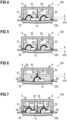
- the temperature is at least a first temperature T2 1 , and the circuit carrier 2 bends, as illustrated in Figure 3B , due to the temperature rise so that a gap (a distance) between the lid 50 (e.g.
- the first mass 61 is cured while all over the circuit carrier 2, the temperature is kept at at least the first temperature T2 1 .
- the cured first mass 61 serves to keep a minimum distance between the substrate assembly 1 and the module housing 5 (e.g. the plunger 55 or the end 551). In order to approximately adjust that minimum distance to a distance which would occur if the electronic module assembly would be operated without the cured first mass 61, curing the first mass 61 may take place in a state in which the temperature of the circuit carrier 2 is closer to its maximum operating temperature which is significantly higher than room temperature.
- the duration for which the circuit carrier 2 is kept in the heated state may be at least 15 minutes, at least 30 minutes, or even at least 60 minutes.
- the first mass 61 may be paste-like, and, subsequently, be cured.
- the first mass 61 may reach its cured state within that duration.
- the cured fist mass substantially prevents a bending-back of the circuit carrier 2 even when the temperature of the circuit carrier 2 subsequently is reduced.
- the first mass 61 is an adhesive, a first adhesive connection between the lid 50 (e.g. between the plunger 55) and the substrate assembly 1 is formed by curing the cured first mass 61.
- the temperature is less than or equal to an initial temperature T2 0 lower than the first temperature T2 1 .
- the initial temperature T2 0 may be, without being restricted to, room temperature, e.g. 25°C
- the first temperature T2 1 may be significantly higher than room temperature, e.g., without being restricted to, 100°C, or 125°C, or 150°C, or even 175°C.
- a difference between the first temperature T2 1 and the initial temperature T2 0 may be at least 75°C.
- Figure 3A illustrates the described initial state, in which, all over the circuit carrier 2, the temperature is less than or equal to an initial temperature T2 0 lower than the first temperature T2 1 .
- the first mass 61 is uncured (i.e. has not yet reached its cured state), and the second mass 62 is uncured, and the surface 2b may be plane or substantially plane. However, the surface 2b might also be slightly concave, or even slightly convex.
- the first mass 61 may reach its cured state simultaneously with or after the second mass 62 reaches its cured state.
- the cured state of the second mass 62 is reached as soon as the second mass 62 everywhere has a modulus of elasticity of at least 0.1 MPa.
- the circuit carrier 2 over the whole heat exchange surface 2b or at least in a region of the heat exchange surface 2b opposite the cured first mass 61, is convex.
- the uncured first mass 61 extends (at least) between the lid 50 (e.g. between the plunger 55) and the substrate assembly 1.
- the circuit carrier 2 bends due to the temperature rise. Therefore, the distance between the lid 50 (e.g. between the plunger 55) and the circuit carrier 2 changes. The bending of the circuit carrier 2 may take place such that the distance between the lid (e.g. between the plunger 55) and the circuit carrier 2 in the heated state is larger than in the initial state.
- the first mass 61 is cured so that the (enlarged) distance between the lid 50 (e.g. the plunger 55) and the circuit carrier 2 is substantially fixed (apart from a possible elastic deformation of the cured mass 61).
- the second mass 62 which is an adhesive, is also cured. Thereby, a (second) adhesive connection is formed between the module housing 5 and the circuit carrier 2. That is, the cured second mass 62 connects the module housing 5 and the circuit carrier 2. In both the uncured and the cured state, the second mass 62 extends (at least) between the module housing 5 and the substrate assembly 1, i.e. (at least) between the module housing 5 and the circuit carrier 2.
- the uncured and the cured second mass 62 may be ring-shaped and seal a ring-shaped gap between the module housing 5 and the circuit carrier 2. The second mass 62 may reach its cured state prior to or simultaneous with the first mass 61.
- the second mass 62 When the second mass 62 reaches its cured state before the first mass 61 reaches its cured state, for instance, when the second mass 62 reaches its cured state when the circuit carrier 2 is still in its initial state (i.e. when all over the circuit carrier 2 the temperature is less than or equal to the initial temperature T2 0 ) or when the circuit carrier 2 is between its initial state and its heated state (i.e.
- the uncured first mass 61 when there is at least one location on or inside the circuit carrier 2 that has a temperature of more than the initial temperature T2 0 and less than the first temperature T2 1 ), the uncured first mass 61 is, to a certain degree, viscous and may be thixotropic so that it does not, on the one hand, flow off and, on the other hand, can follow the bending of the circuit carrier 2 in that it extends, at all times between the initial state of the circuit carrier 2 and the time at which the first mass 61 reaches its cured state (in particular at all times between the initial state of the circuit carrier 2 and the time at which the second mass 62 reaches its cured state), between the plunger 55 (e.g. between the end 551) and the substrate assembly 1 (e.g. the circuit carrier 2).
- the first mass 61 "follows" the bending of the circuit carrier 2 so that the first mass 61 bridges the gap between the lid 50 (e.g. between the plunger 55) and the substrate assembly 1 at all times.
- the substrate assembly 1, the module housing 5, the cured first mass 61 and the cured second mass 62 become constituents of an electronic module assembly 100, and the circuit carrier 2 may be cooled down so that everywhere on and in the circuit carrier 2 the temperature is less than or equal to a second temperature T2 2 that is lower than the first temperature T2 1 .
- This state is illustrated in Figure 3C .
- the difference between the second temperature T2 2 and the first temperature T2 1 may be, without being restricted to, at least 75°C.
- the second temperature T2 2 may be less than or equal to 25°C.
- the cooled down circuit carrier 2 substantially keeps its bent shape because the cured first mass 61 prevents (apart from an elastic deformation of the cured first mass 61) a reduction of the distance d15 (see Figure 3D ) between the lid 50 (e.g. between the plunger 55) and the substrate assembly 1, and because the module housing 5 is significantly stiffer than the circuit carrier 2.
- the distance d15 between the lid 50 (e.g. between the plunger 55) and the substrate assembly 1 may be, without being restricted to, less than 0.5 mm.
- a dielectric potting 63 for instance a gel (e.g. a silicone gel) may be disposed inside the module housing 5.
- the potting 63 may adjoin the circuit carrier 2, the side wall 51, 52, 53, 54, the second mass 62, and, optionally, also the first mass 61.
- the potting 63 may cover the semiconductor chip 10 and, if provided, the bonding wire 3.
- a layer 7 of a thermal interface material that may be produced on a heat exchange surface 2b of the circuit carrier 2 which is a surface 2b of the circuit carrier 2 facing away from the lid 50 and, if the module housing 5 has a plunger 55, from the plunger 55. That is, the circuit carrier 2 is disposed between the plunger 55 and the layer 7 of a thermal interface material. Instead of this, it would also be possible to produce the layer 7 of the thermal interface material on the heat sink 200. In both cases, the thermal interface material may have, at a temperature of 25°C and without being restricted to, a thermal conductivity in the range from 0.4 W/(m ⁇ K) to 1 W/(m ⁇ K).
- the layer 7 applied to the heat exchange surface 2b of the circuit carrier 2 or to the heat sink 200 is a continuous layer it may have, without being restricted to, a layer thickness d7 of less than or equal to 30 ⁇ m so that the down force F required for letting creep a little of the thermal interface material laterally out of the gap between the heat exchange surface 2b and the heat sink 200 is very low.
- the layer thickness d7 may be, without being restricted to, less than or equal to 120 ⁇ m.
- the footprint area of each single dot may be less than or equal to 10 mm 2 .
- the total amount of the thermal interface material may be chosen such that an average thickness of the layer 7 is less than or equal to 30 ⁇ m.
- the module housing 5 and a heat sink 200 may be joined so that the layer 7 of the thermal interface material adjoins both the circuit carrier 2 (i.e. the heat exchange surface 2b) and the heat sink 200, and so that the circuit carrier 2 is pressed against the heat sink 200.
- the module housing 5 and the heat sink 200 are joined by screws 9.
- any other joining technique e.g. clamping, riveting, may be used as well.
- the circuit carrier 2 is pressed against the heat sink 200 so that the bending of the circuit carrier 2 is reduced.
- the module housing 5 is pre-tensioned, which causes the lid 50 (e.g.
- the plunger 55 to locally press the substrate assembly 1 indirectly (i.e. via the cured first mass 61) against the heat sink 200.
- This pressing counteracts the formation of air gaps or other gas-filled spaces between the circuit carrier 2 (i.e. between the heat exchange surface 2b) and the heat sink 200 when the circuit carrier 2 is heated during the operation of the electronic module assembly 100 by the heat produced from the electronic components 10 of the substrate assembly 1.
- the downforce F caused by the pretension of the module housing 5 is schematically indicated by a bold arrow.
- heating the circuit carrier 2 causes the circuit carrier 2 to bend towards the lid 50 (e.g.
- the uncured and cured first mass 61 was described to adjoin the substrate assembly 1 at the circuit carrier 2, e.g. the first metallization layer 21.
- the principles, methods, designs, dimensions, options, materials etc. of the examples explained above also apply if the uncured and cured first mass 61 adjoins the substrate assembly 1 at the semiconductor chip 10 (see Figure 4 ), at the insulation carrier 20 (see Figure 5 ) or at a bonding wire 3 (e.g. at a region of a maximum loop height of the bonding wire 3) (see Figure 6 ), or at any other constituent part of the substrate assembly 1.
- a module housing 5 may include two or more plungers 55, and between each of the plungers 55 and the substrate assembly 1 a curable first mass 61 may be placed and subsequently cured as described above. If the first mass 61 is an adhesive, the cured first mass 61 forms a substance-to-substance bond between the respective plunger 55 and the substrate assembly 1.
- the difdifferent uncured and cured first masses 61 may optionally be disposed distant from one another and/or, also optionally, distant from both the uncured and cured second mass 62.
- a circuit carrier 2 having edge lengths of about 50 mm x 50 mm, an insulation carrier 20 of Al 2 O 3 , a first substrate metallization layer 21 and a second substrate metallization layer 22 of copper were used.
- the layer thickness d20 of the insulation carrier 20 was 0.38 mm, and each of the layer thicknesses d21 and d22 of substrate metallization layers 21, 22 was 0.3 mm.
- the required downforce F was between 5 N and 10 N, the distance d15 was about 0.1 mm, the plunger was a straight pin and had a cross section of about 5 mm 2 , and the modulus of elasticity of the cured first mass 61 was, at a temperature of 25°C, about 20 MPa.
- the uncured and cured first mass 61 does not necessarily need to be disposed between the substrate assembly 1 and a plunger 55. Instead, the uncured first mass 61 may be applied between the substrate assembly 1 and a section 501 of the lid 50 where the lid 50 has no plunger, and then be cured so that the cured first mass 61 is disposed between the substrate assembly 1 (e.g. between a bonding wire 3 of the substrate assembly 1) and the plunger-free section 501 of the lid 50. For instance, the cured first mass 61 may extend between the cured first mass 61 and the substrate assembly 1 (e.g. a bonding wire 3). Apart from the fact that there is no plunger in the section 501, the principles, methods, designs, dimensions, options, materials etc. of the examples explained above also apply.
- a dielectric potting 63 for instance a gel (e.g. a silicone gel) is disposed inside the module housing 5 and if the first mass 61 extends between a bonding wire 3 and the lid 50 (e.g. between a bonding wire 3 and the plunger 55 or the end 551), the bonding wire 3 may be completely embedded in the potting 63 as illustrated in Figures 6, 7 and 8 . Alternatively, the bonding wire 3 may protrude from the potting 63, and the first mass 61 may extend between the protruding part of the bonding wire 3 and the lid 50.
- a dielectric potting 63 for instance a gel (e.g. a silicone gel) is disposed inside the module housing 5 and if the first mass 61 extends between a bonding wire 3 and the lid 50 (e.g. between a bonding wire 3 and the plunger 55 or the end 551)
- the bonding wire 3 may be completely embedded in the potting 63 as illustrated in Figures 6, 7 and 8 .
- an electronic module assembly 100 may include two or more separate substrate assemblies 1 disposed distant from one another.
- Each of the substrate assemblies 1 may, irrespective of the structure of the other substrate assemblies 1, have the properties of any of the substrate assemblies 1 explained above and be attached to the module housing 5 using curable first and second masses 61, 62 as explained above.
- the module housing 5 may have at least one plunger 55, and a curable first mass 61 may be disposed between that plunger 55 and the respective substrate assembly 1.
- the module housing 5 may have at least one plunger 55, and a curable first mass 61 may be disposed between that plunger 55 and the respective substrate assembly 1 (as explained with reference to Figures 1 to 7 ), and for each of at least one further substrate assembly 1, a curable first mass 61 may be disposed between a plunger-free section 501 of the module housing 5 and the respective substrate assembly 1 (as explained with reference to Figure 8 ).
- a curable first mass 61 may be disposed between a plunger-free section 501 of the module housing 5 and the respective substrate assembly 1 (as explained with reference to Figure 8 ).
- each of the substrate assemblies 1 may include a circuit carrier 2 having a heat exchange surface 2b.
- a layer 7 of a thermal interface material having the properties explained with reference to Figure 3E has been produced.
- the electronic module assembly 100 with layers 7 of the thermal interface material applied to the heat exchange surfaces 2b may be joined with a heat sink 200 as explained in more detail with reference to Figure 3F .
- the circuit carriers 2 are pressed against the heat sink 200 so that the bending of the circuit carriers 2 is reduced.
- the module housing 5 is pre-tensioned which causes the lid 50 (e.g. the plungers 55) to locally press the substrate assemblies 1 indirectly (i.e. via the respective cured first mass 61) against the heat sink 200.
- the downforces F caused by the pretension of the module housing 5 are schematically indicated by bold arrows.
- a downforce F caused by a pre-tension of the module housing 5 is transmitted from the module housing 5 (e.g. from the lid 50, e.g. from a plunger 55 or a plunger-free section 501) via a cured first mass 61.
- the cured first mass 61 may have a high modulus of elasticity which may be higher than the moduli of elasticity of many adhesives used in conventional electronic modules for joining a circuit carrier and a module housing.
- the cured first mass 61 may, without being restricted to, everywhere comprise, at a temperature of 25°C, a modulus of elasticity of at least 1 MPa or even of at least 15 MPa.
- the cured second mass 62 may, without being restricted to, everywhere comprise, at a temperature of 25°C, a modulus of elasticity of at least 0.1 MPa.
- both the cured first mass 61 and the cured second mass 62 may everywhere comprise, at a temperature of 25°C, the same modulus of elasticity, e.g. at least 1 MPa.
- Such identical moduli of elasticity can easily by achieved by producing the cured first and second masses 61, 62 from the same type of curable mass.
- the cured first mass 61 is disposed distant from each edge of the insulation carrier 20 of the circuit carrier 2 of the substrate assembly 1.
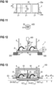
- Figure 10 is a cross-sectional top view of the electronic module assembly 100 of Figure 3C illustrating just the circuit carrier 2, the cured first mass 61 and the plunger 55. For the sake of clarity, the other parts of the electronic module assembly 100 are omitted.
- the insulation carrier 20 of the circuit carrier 2 has a number of edges 20e. The shortest among all distances between the cured first mass 61 and all edges 20e is designated with d0. For instance, the shortest distance d0 may be, without being restricted to, 10 mm.
- Figure 3D illustrates an enlarged section of an electronic module assembly 100 according to Figure 3C that includes a module housing with a lid having a plunger 55, shown after cooling down the circuit carrier 2 from the heated state to the cooled-down state, so that everywhere on and in the circuit carrier 2 the temperature is less than or equal to the second temperature T2 2 .
- a part of the plunger 55 is embedded in the cured first mass 61.
- there is no layer 7 of a thermal interface material applied to the surface 2b (as in Figure 3E ), and the electronic module assembly 100 is not mounted to a heat sink 200 (as in Figure 3F ).
- FIG 11 is a cross-sectional top view showing just the plunger 55 and the cured first mass 61 with the cross-section being taken in a cross-sectional plane E4-E4 shown in Figure 3D .
- the cross-sectional plane E4-E4 intersects both the plunger 55 and the cured first mass 61 perpendicularly to the direction of the downforce F and is taken such that in the cross-sectional plane E4-E4, the cured first mass 61 surrounds the plunger 55 and adjoins the entire circumference of the plunger 55.
- the cross-sectional area of the plunger 55 is A55.
- the modulus of elasticity of the cured first mass 61 is sufficiently high to generate a proper downforce F and to prevent the surface 2b of the cooled-down circuit carrier 2 adhered to the module housing 5 (see Figure 3C ) from being concave.
- a concave surface 2b is undesired because it would cause an accumulation of the thermal interface material when the electronic module assembly 100 provided with the layer 7 of the thermal interface material is mounted on the heat sink 200.
- a method for estimating a proper downforce F is, as illustrated in Figure 12 , to take a sample 1' of the substrate assembly 1 (i.e. an identical copy thereof) to be used in the electronic module assembly 100.
- the sample substrate assembly 1' is heated to the heated state and subsequently cooled down to the cooled state as described above because it has been shown that, after such temperature cycling, the reproducibility of the thermomechanical behavior of a substrate assembly 1, 1' is significantly improved.
- the border of circuit carrier 2 is, as illustrated in the measuring arrangement of Figure 12 , supported at its border by a stable support 300.
- the circuit carrier 2 resting on the support 300 is deflected by locally pressing against the sample substrate assembly 1' so that the position of the force effect is shifted by a pre-defined distance d2, e.g. 10 ⁇ m or 30 ⁇ m, and the circuit carrier 2 becomes convex or more convex at the surface 2b.
- the local pressing against the sample substrate assembly 1' takes place at the corresponding position at which the first mass 61 (illustrated in dashed fashion) is to be placed in the electronic module assembly 100 to be produced.
- the dotted line illustrates the run of the surface 2b when the desired pre-defined distance d2 is reached.
- a force measuring device 400 is used to measure a force F TEST required to achieve the desired pre-defined distance d2.
- the force F TEST is taken as the desired (target) down force F explained with reference to Figure 3F .
- the method also may be used in connection with all other electronic modules 100 in which a cured first mass 61 is (at least) disposed between a substrate assembly 1 and a straight plunger 55.
- the local pressing against the sample substrate assembly 1' takes place at the corresponding position at which the first mass 61 is to be placed on the substrate assembly 1 of the electronic module assembly 100 to be produced, e.g. at the first substrate metallization layer 21 ( Figure 3C ), at a semiconductor chip 10 ( Figure 4 ), at the insulation carrier 20 ( Figure 5 ), or at a bonding wire 3 ( Figure 6 ).
- the shapes the heat exchange surface 2b of an electronic module assembly 100 takes at two different temperatures of the electronic module assembly 100 are illustrated.
- the shape the heat exchange surface takes when the electronic module assembly 100 everywhere has a low temperature T low is designated with 2b(T low )
- the shape the heat exchange surface takes when the electronic module assembly 100 everywhere has a high temperature T high higher than the low temperature T low is designated with 2b(T high ) and illustrated in dashed fashion.
- the curvature of the heat exchange surface (2b(T high )) at the high temperature T high of the electronic module assembly 100 is greater than the curvature of the heat exchange surface (2b(T low) ) at the low temperature T low .
- a distance between a point P of the heat exchange surface 2b opposite the cured first mass 61 and a tangent plane E3-E3 of the module housing 5 may depend on the temperature of the electronic module assembly 100.
- a point P of the heat exchange surface 2b is located opposite the cured first mass 61 (and, if there is a plunger 55, opposite the plunger 55 or the opposite the end 551) at a position P low .
- the distance between this point P and the tangential plane E3-E3 at the low temperature T low of the electronic module assembly 100 is designated with dP low , and the distance between this point P (i.e.
- the distances dP high and dP low differ from one another.
- the high temperature T high is at least the first temperature T2 1 (i.e. the minimum temperature the circuit carrier 2 has in its heated state) and the low temperature T low is less than or equal to the second temperature T22 (i.e. the maximum temperature the circuit carrier 2 has in its cooled state)
- the absolute value of the difference between the distances dP high and dP low may be, without being restricted to, at least 10 ⁇ m.
- the distance dP high may be greater than the distance dP low .
- the tangent plane E3-E3 may be a (virtual) plane abutting the side of the module housing 5 to which the circuit carrier 2 mounted.
- a distance between such a point P and the lid 50 may change with the temperature of the electronic module assembly 100. This is, analogously to Figure 13 , illustrated in Figure 14 .
- the distance between the point P and the lid 50 (which in the example of Figure 14 is the distance between the point P and the plunger 55 or the end 551) at the low temperature T low of the electronic module assembly 100 is designated with aP low
- the distance between this point P and the lid 50 at the high temperature T high of the electronic module assembly 100 is designated with aP high
- the distances aP high and aP low differ from one another. For instance, if the high temperature T high is at least the first temperature T2 1 (i.e. the minimum temperature the circuit carrier 2 has in its heated state) and the low temperature T low is less than or equal to the second temperature T22 (i.e.
- the difference aP high - aP low between the distances aP high and aP low may be, without being restricted to, at least 10 ⁇ m. Thereby, the distance dP high is greater than the distance dP low .
- the module housing 5 e.g. the plunger 55 or the end 551 exerts a force F on the circuit carrier 2 so that the cured first mass 61 is compressed.
- the compression can be expressed in terms of a change ⁇ d15 of the distance d15 (see Figure 3D ) between a state in which the electronic module assembly 100 is in the unmounted state (i.e. when the electronic module assembly 100 is not mounted to a heat sink or the like so that the bending of the circuit carrier 2 is not limited by external elements) and a state in which the electronic module assembly 100 is in a mounted state (i.e.
- the distance d15 is as explained with reference to Figure 3D .
- F A55 ⁇ E61 ⁇ ⁇ d15/d15 .
- A55 is the cross-sectional area of the plunger 55 as explained with reference to Figure 11
- E61 is the modulus of elasticity E61 of the cured first mass 61.
- the resulting force F is about 9.8 N.
- the resulting force F is about 5.7 N.
Landscapes
- Engineering & Computer Science (AREA)
- Microelectronics & Electronic Packaging (AREA)
- Physics & Mathematics (AREA)
- Power Engineering (AREA)
- Condensed Matter Physics & Semiconductors (AREA)
- General Physics & Mathematics (AREA)
- Computer Hardware Design (AREA)
- Chemical & Material Sciences (AREA)
- Materials Engineering (AREA)
- Dispersion Chemistry (AREA)
- Ceramic Engineering (AREA)
- Thermal Sciences (AREA)
- Manufacturing & Machinery (AREA)
- Cooling Or The Like Of Semiconductors Or Solid State Devices (AREA)
Claims (12)
- Verfahren zur Herstellung einer elektronischen Modulanordnung, wobei das Verfahren aufweist:Aushärten einer aushärtbaren ersten Masse (61), die sich zwischen einer Substratanordnung (1) und einem Deckel (50) eines Modulgehäuses (5) erstreckt, während ein Schaltungsträger (2) der Substratanordnung (1) auf einer Temperatur von mindestens einer ersten Temperatur ist, wobei der Schaltungsträger (2) einen dielektrischen Isolationsträger (20) und eine an dem dielektrischen Isolationsträger (20) angebrachte erste Substratmetallisierungsschicht (21) umfasst, und wobei die Substratanordnung (1) ferner mindestens einen Halbleiterchip (10) aufweist, der mit der ersten Substratmetallisierungsschicht (21) verbunden ist;Bilden einer Klebeverbindung zwischen einer Seitenwand (51, 52, 53, 54) des Modulgehäuses (5) und dem Schaltungsträger (2) durch Aushärten einer aushärtbaren zweiten Masse (62);Abkühlen des Schaltungsträgers (2) auf unter eine zweite Temperatur, die niedriger als die erste Temperatur ist, nach dem Aushärten der aushärtbaren ersten Masse (61); wobeidie ausgehärtete erste Masse (61) sich entfernt von den Kanten des Schaltungsträgers (2) und gegenüber einer Wärmetauschfläche (2b) des Schaltungsträgers (2) befindet,der Schaltungsträger (2) von einem anfänglichen Zustand auf einen erwärmten Zustand erwärmt wird, in dem die Temperatur des Schaltungsträgers (2) auf der Temperatur von mindestens der ersten Temperatur ist,der Schaltungsträger sich aufgrund des Temperaturanstiegs biegt,die aushärtbare erste Masse (61) ausgehärtet wird, wenn der Schaltungsträger im gebogenen Zustand ist,die aushärtbare erste Masse (61) sich zwischen dem Modulgehäuse (5) und der Substratanordnung (1) erstreckt und einen Spalt zwischen dem Modulgehäuse (5) und der Substratanordnung (1) überbrückt, der zunimmt, wenn der Schaltungsträger (2) sich aufgrund des Temperaturanstiegs biegt, unddie ausgehärtete erste Masse (61) den Spalt so fixiert, dass der Schaltungsträger (2) nach dem Abkühlen im gebogenen Zustand bleibt.
- Verfahren nach Anspruch 1, wobei eine Differenz zwischen der zweiten Temperatur und der ersten Temperatur mindestens 75 °C beträgt und wobei die elektronische Modulanordnung (100) derart hergestellt wird, dassein Punkt der Wärmetauschfläche (2) gegenüber der ersten ausgehärteten Masse (61) einen ersten Abstand von einem Deckel (50) des Modulgehäuses (5) aufweist, wenn die elektronische Modulanordnung (100) mindestens auf die erste Temperatur erwärmt wird;der Punkt der Wärmetauschfläche (2) einen zweiten Abstand vom Deckel (50) des Modulgehäuses (5) aufweist, wenn das elektronische Modulanordnung (100) auf unter die oder gleich der zweiten Temperatur erwärmt wird; undeine Differenz zwischen dem ersten Abstand und dem zweiten Abstand mindestens 10 µm beträgt.
- Verfahren nach Anspruch 1 oder 2, wobei das Aushärten der ersten aushärtbaren Masse (61), das Bilden der Klebeverbindung und das Abkühlen des Schaltungsträgers (2) derart durchgeführt werden, dass mindestens eines von Folgenden zutrifft:die ausgehärtete erste Masse (61) weist überall einen Elastizitätsmodul von mindestens 1 MPa auf;die ausgehärtete zweite Masse (62) weist überall einen Elastizitätsmodul von mindestens 0,1 MPa auf.
- Verfahren nach einem der vorhergehenden Ansprüche, wobei das Aushärten der aushärtbaren ersten Masse (61), das Bilden der Klebeverbindung und das Abkühlen des Schaltungsträgers (2) derart durchgeführt werden, dass sowohl die ausgehärtete erste Masse (61) als auch die ausgehärtete zweite Masse (62) überall einen Elastizitätsmodul von mindestens 1 MPa aufweisen.
- Verfahren nach einem der Ansprüche 1 bis 4, wobei:
das Modulgehäuse (5) einen Kolben (55) aufweist, der zwischen einem ersten Segment (51) und einem zweiten Segment (52) der Seitenwand und von beiden entfernt angeordnet ist, wobei der Kolben (55) ein Vorsprung des Deckels (50) des Modulgehäuses (5) ist. - Verfahren nach Anspruch 5, wobei:der Kolben (55) ein freies Ende (551) aufweist; unddas Aushärten der aushärtbaren ersten Masse (61), das Bilden der Klebeverbindung und das Abkühlen des Schaltungsträgers (2) derart durchgeführt werden, dass die ausgehärtete erste Masse (61) sowohl an das freie Ende (551) als auch an die Substratanordnung (1) angrenzt.
- Verfahren nach einem der Ansprüche 1 bis 6, wobei das Aushärten der ersten aushärtbaren Masse (61), das Bilden der Klebeverbindung und das Abkühlen des Schaltungsträgers (2) derart durchgeführt werden, dass:
im ausgehärteten Zustand der aushärtbaren ersten Masse (61) ein Abstand zwischen dem Deckel (50) des Modulgehäuses (5) und der Substratanordnung (1) an einer Stelle, an der sich die ausgehärtete erste Masse (61) befindet, kleiner als 0,5 mm ist. - Verfahren nach einem der vorhergehenden Ansprüche, wobei das Aushärten der ersten aushärtbaren Masse (61), das Bilden der Klebeverbindung und das Abkühlen des Schaltungsträgers (2) derart durchgeführt werden, dass:
die ausgehärtete erste Masse (61) an mindestens eines von Folgenden angrenzt:den Schaltungsträger (2);einen Bonddraht (8) der Substratanordnung (1);einen Halbleiterchip (10) der Substratanordnung (1). - Verfahren nach einem der vorhergehenden Ansprüche, wobei mindestens eines von Folgendem zutrifft:die erste Temperatur beträgt mindestens 100 °C;die zweite Temperatur ist unter oder gleich 25 °C.
- Verfahren nach einem der vorhergehenden Ansprüche, aufweisend:
Anordnen eines dielektrischen Gels innerhalb des Modulgehäuses (5), wobei das Gel an den Schaltungsträger (2), die Seitenwand (51, 52, 53, 54) und mindestens eine der aushärtbaren ersten Masse (61) und der zweiten Masse (62) angrenzt. - Verfahren nach einem der vorhergehenden Ansprüche, aufweisend:Herstellen einer Schicht (7) aus einem Wärmeleitmaterial auf dem Schaltungsträger (2);Verbinden des Modulgehäuses (5) und einer Wärmesenke (200) so, dass die Schicht (7) aus dem Wärmeleitmaterial sowohl an den Schaltungsträger (2) als auch die Wärmesenke (200) angrenzt und dass der Schaltungsträger (2) gegen die Wärmesenke (200) gedrückt wird.
- Elektronische Modulanordnung, aufweisend:eine Substratanordnung (1), wobei die Substratanordnung (1) einen Schaltungsträger (2) aufweist, wobei der Schaltungsträger (2) einen dielektrischen Isolationsträger (20) und eine an dem dielektrischen Isolationsträger (20) angebrachte erste Substratmetallisierungsschicht (21) aufweist, und wobei die Substratanordnung (1) ferner mindestens einen Halbleiterchip (10) aufweist, der mit der ersten Substratmetallisierungsschicht (21) verbunden ist;ein Modulgehäuse (5), das mit dem Schaltungsträger (2) durch eine Klebeverbindung verbunden ist, die durch eine zweite ausgehärtete Masse (62) zwischen einer Seitenwand (51, 52, 53, 54) des Modulgehäuses und dem Schaltungsträger (2) gebildet wird;eine ausgehärtete erste Masse (61), die sich zwischen der Substratanordnung (1) und einem Deckel (50) des Modulgehäuses (5) erstreckt und einen Spalt zwischen dem Modulgehäuse (5) und der Substratanordnung (1) überbrückt; undeine Wärmetauschfläche (2b), die durch eine Oberfläche des Schaltungsträgers (2) gebildet wird, die von der ausgehärteten ersten Masse (61) abgewandt ist;wobeidie ausgehärtete erste Masse (61) sich entfernt von den Kanten des Schaltungsträgers (2) befindet,der Schaltungsträger (2) vom Modulgehäuse (5) weg gebogen ist und durch die ausgehärtete erste Masse (61), die sich über den Spalt zwischen dem Modulgehäuse (5) und der Substratanordnung (1) erstreckt und diesen fixiert, in dem gebogenen Zustand fixiert wird und mindestens eine Region der Wärmetauschfläche (2b) gegenüber der ausgehärteten ersten Masse (61) konvex ist.
Priority Applications (3)
| Application Number | Priority Date | Filing Date | Title |
|---|---|---|---|
| EP16206797.9A EP3340291B1 (de) | 2016-12-23 | 2016-12-23 | Verfahren zur herstellung einer elektronischen modulanordnung und elektronische modulanordnung |
| US15/852,158 US10462921B2 (en) | 2016-12-23 | 2017-12-22 | Method for producing an electronic module assembly and electronic module assembly |
| CN201711424717.9A CN108242401B (zh) | 2016-12-23 | 2017-12-25 | 用于制造电子模块组件的方法和电子模块组件 |
Applications Claiming Priority (1)
| Application Number | Priority Date | Filing Date | Title |
|---|---|---|---|
| EP16206797.9A EP3340291B1 (de) | 2016-12-23 | 2016-12-23 | Verfahren zur herstellung einer elektronischen modulanordnung und elektronische modulanordnung |
Publications (2)
| Publication Number | Publication Date |
|---|---|
| EP3340291A1 EP3340291A1 (de) | 2018-06-27 |
| EP3340291B1 true EP3340291B1 (de) | 2024-10-30 |
Family
ID=57749737
Family Applications (1)
| Application Number | Title | Priority Date | Filing Date |
|---|---|---|---|
| EP16206797.9A Active EP3340291B1 (de) | 2016-12-23 | 2016-12-23 | Verfahren zur herstellung einer elektronischen modulanordnung und elektronische modulanordnung |
Country Status (3)
| Country | Link |
|---|---|
| US (1) | US10462921B2 (de) |
| EP (1) | EP3340291B1 (de) |
| CN (1) | CN108242401B (de) |
Families Citing this family (32)
| Publication number | Priority date | Publication date | Assignee | Title |
|---|---|---|---|---|
| JP6274196B2 (ja) * | 2015-12-16 | 2018-02-07 | 株式会社オートネットワーク技術研究所 | 電気接続箱 |
| KR102391008B1 (ko) * | 2017-08-08 | 2022-04-26 | 현대자동차주식회사 | 파워 모듈 및 그 파워 모듈을 포함하는 전력 변환 시스템 |
| US10850623B2 (en) | 2017-10-30 | 2020-12-01 | Sf Motors, Inc. | Stacked electric vehicle inverter cells |
| US10790758B2 (en) | 2018-03-08 | 2020-09-29 | Chongqing Jinkang New Energy Vehicle Co., Ltd. | Power converter for electric vehicle drive systems |
| JP7043904B2 (ja) * | 2018-03-13 | 2022-03-30 | 富士電機株式会社 | センサ装置およびその製造方法 |
| US10779445B2 (en) | 2018-03-23 | 2020-09-15 | Chongqing Jinkang New Energy Vehicle Co., Ltd. | Inverter module having multiple half-bridge modules for a power converter of an electric vehicle |
| US10756649B2 (en) | 2018-03-23 | 2020-08-25 | Chongqing Jinkang New Energy Vehicle Co., Ltd. | Inverter module having multiple half-bridge modules for a power converter of an electric vehicle |
| US10778118B2 (en) | 2018-03-23 | 2020-09-15 | Chongqing Jinkang New Energy Vehicle Co., Ltd. | Inverter module having multiple half-bridge modules for a power converter of an electric vehicle |
| US10772242B2 (en) | 2018-04-17 | 2020-09-08 | Chongqing Jinkang New Energy Vehicle Co., Ltd. | Inverter module of an electric vehicle |
| US10778117B2 (en) | 2018-04-17 | 2020-09-15 | Chongqing Jinkang New Energy Vehicle Co., Ltd. | Inverter module of an electric vehicle |
| US10660242B2 (en) | 2018-04-26 | 2020-05-19 | Chongqing Jinkang New Energy Vehicle Co., Ltd. | Electric vehicle inverter module heat sink |
| US10600577B2 (en) * | 2018-04-26 | 2020-03-24 | Sf Motors, Inc. | Electric vehicle inverter module capacitors |
| US10600578B2 (en) * | 2018-04-26 | 2020-03-24 | Sf Motors, Inc. | Electric vehicle inverter module capacitors |
| US10608423B2 (en) | 2018-04-26 | 2020-03-31 | Sf Motors, Inc. | Electric vehicle inverter module laminated bus bar |
| DE102019207341A1 (de) * | 2019-05-20 | 2020-11-26 | Robert Bosch Gmbh | Elektronikbaugruppe und Elektronikanordnung |
| US11302682B2 (en) * | 2019-10-25 | 2022-04-12 | Advanced Semiconductor Engineering, Inc. | Optical device package |
| CN113053802A (zh) * | 2019-12-27 | 2021-06-29 | 台湾积体电路制造股份有限公司 | 半导体器件的形成方法 |
| US20210242098A1 (en) * | 2020-02-03 | 2021-08-05 | International Business Machines Corporation | Variable thickness lid adhesive |
| US10893604B1 (en) * | 2020-03-03 | 2021-01-12 | Goodrich Corporation | Potted printed circuit board module and methods thereof |
| EP3913665B1 (de) * | 2020-05-18 | 2025-04-02 | Infineon Technologies AG | Leistungshalbleitermodul und verfahren zur herstellung eines leistungshalbleitermoduls |
| EP3929973B1 (de) * | 2020-06-22 | 2022-10-26 | Infineon Technologies AG | Leistungshalbleitermodul und verfahren zur herstellung eines leistungshalbleitermoduls |
| EP3979313B1 (de) | 2020-09-30 | 2022-11-30 | SEMIKRON Elektronik GmbH & Co. KG | Leistungselektronische einrichtung und leistungshalbleitermodul damit |
| FR3115653B1 (fr) * | 2020-10-22 | 2022-09-09 | Continental Automotive Gmbh | Elément de boitier électronique comprenant un radiateur et procédé d’ajustement associé |
| US12157217B2 (en) | 2021-03-15 | 2024-12-03 | Milwaukee Electric Tool Corporation | Potting boat heat sink |
| JP2023031825A (ja) * | 2021-08-25 | 2023-03-09 | 富士電機株式会社 | 半導体装置及び半導体装置の製造方法 |
| JP2023042658A (ja) * | 2021-09-15 | 2023-03-28 | 富士電機株式会社 | 半導体装置 |
| JP2023128645A (ja) * | 2022-03-04 | 2023-09-14 | 富士電機株式会社 | 半導体装置の製造方法 |
| JP2025512142A (ja) * | 2022-04-28 | 2025-04-17 | ヒタチ・エナジー・リミテッド | 半導体パワーモジュールおよび半導体パワーモジュールを製造するための方法 |
| CN115346974B (zh) * | 2022-08-10 | 2025-09-05 | 西安微电子技术研究所 | 一种抗辐照负载点电源的多基板堆叠结构及其组装方法 |
| CN116344404A (zh) * | 2023-04-06 | 2023-06-27 | 长园半导体设备(珠海)有限公司 | Igbt模块封装自动化系统及其封装方法 |
| CN119277689A (zh) * | 2023-07-04 | 2025-01-07 | 台达电子工业股份有限公司 | 具有防泄漏结构的电子模块 |
| AT527909B1 (de) * | 2024-01-16 | 2025-08-15 | Miba Sinter Austria Gmbh | Kühlvorrichtung |
Family Cites Families (8)
| Publication number | Priority date | Publication date | Assignee | Title |
|---|---|---|---|---|
| JP2003303933A (ja) * | 2002-04-12 | 2003-10-24 | Toyota Motor Corp | 半導体装置の製造方法 |
| US7268428B2 (en) * | 2005-07-19 | 2007-09-11 | International Business Machines Corporation | Thermal paste containment for semiconductor modules |
| US20080128897A1 (en) * | 2006-12-05 | 2008-06-05 | Tong Wa Chao | Heat spreader for a multi-chip package |
| JP6480098B2 (ja) * | 2013-10-31 | 2019-03-06 | 三菱電機株式会社 | 半導体装置 |
| KR102340828B1 (ko) * | 2014-10-23 | 2021-12-17 | 삼성전자주식회사 | 인쇄회로기판 어셈블리 제조 방법 |
| JP6421050B2 (ja) * | 2015-02-09 | 2018-11-07 | 株式会社ジェイデバイス | 半導体装置 |
| CN106298689B (zh) * | 2015-05-28 | 2018-10-09 | 台达电子企业管理(上海)有限公司 | 封装结构 |
| ITUB20153344A1 (it) * | 2015-09-02 | 2017-03-02 | St Microelectronics Srl | Modulo di potenza elettronico con migliorata dissipazione termica e relativo metodo di fabbricazione |
-
2016
- 2016-12-23 EP EP16206797.9A patent/EP3340291B1/de active Active
-
2017
- 2017-12-22 US US15/852,158 patent/US10462921B2/en active Active
- 2017-12-25 CN CN201711424717.9A patent/CN108242401B/zh active Active
Also Published As
| Publication number | Publication date |
|---|---|
| CN108242401B (zh) | 2021-10-01 |
| CN108242401A (zh) | 2018-07-03 |
| US20180184538A1 (en) | 2018-06-28 |
| EP3340291A1 (de) | 2018-06-27 |
| US10462921B2 (en) | 2019-10-29 |
Similar Documents
| Publication | Publication Date | Title |
|---|---|---|
| EP3340291B1 (de) | Verfahren zur herstellung einer elektronischen modulanordnung und elektronische modulanordnung | |
| US11631623B2 (en) | Power semiconductor device and method of manufacturing the same, and power conversion device | |
| JP4569473B2 (ja) | 樹脂封止型パワー半導体モジュール | |
| US10104775B2 (en) | Semiconductor device and method for manufacturing the same | |
| US8546923B2 (en) | Rigid power module suited for high-voltage applications | |
| CN107112316B (zh) | 半导体模块 | |
| EP2020683A1 (de) | Halbleiterbauelement und verfahren zu seiner herstellung | |
| US10490491B2 (en) | Semiconductor device | |
| JP2009536458A (ja) | 半導体モジュール及びその製造方法 | |
| US10720368B2 (en) | Semiconductor device and method for manufacturing same | |
| CN107004653A (zh) | 半导体装置以及半导体装置的制造方法 | |
| CN104051397B (zh) | 包括非整数引线间距的封装器件及其制造方法 | |
| JP7555257B2 (ja) | 電気回路体、電力変換装置、および電気回路体の製造方法 | |
| JP5895220B2 (ja) | 半導体装置の製造方法 | |
| EP2804209A1 (de) | Geformtes Elektronikmodul | |
| CN108231613A (zh) | 将电子芯片与连接器主体互连并使连接器主体成形的通用过程 | |
| JP5407881B2 (ja) | パワーモジュール製造方法およびその方法により製造したパワーモジュール | |
| US11626351B2 (en) | Semiconductor package with barrier to contain thermal interface material | |
| JP2010192591A (ja) | 電力用半導体装置とその製造方法 | |
| JP5613100B2 (ja) | 半導体装置の製造方法 | |
| US20210305144A1 (en) | Semiconductor device and manufacturing method thereof | |
| JP2008258435A (ja) | 半導体装置及びその製造方法 | |
| US20240055392A1 (en) | Method of manufacturing semiconductor device | |
| JP2008181922A (ja) | 熱伝導基板、その製造方法および熱伝導基板を用いた半導体装置 | |
| US20240250057A1 (en) | Semiconductor package and method of manufacturing the same |
Legal Events
| Date | Code | Title | Description |
|---|---|---|---|
| PUAI | Public reference made under article 153(3) epc to a published international application that has entered the european phase |
Free format text: ORIGINAL CODE: 0009012 |
|
| STAA | Information on the status of an ep patent application or granted ep patent |
Free format text: STATUS: THE APPLICATION HAS BEEN PUBLISHED |
|
| AK | Designated contracting states |
Kind code of ref document: A1 Designated state(s): AL AT BE BG CH CY CZ DE DK EE ES FI FR GB GR HR HU IE IS IT LI LT LU LV MC MK MT NL NO PL PT RO RS SE SI SK SM TR |
|
| AX | Request for extension of the european patent |
Extension state: BA ME |
|
| STAA | Information on the status of an ep patent application or granted ep patent |
Free format text: STATUS: REQUEST FOR EXAMINATION WAS MADE |
|
| 17P | Request for examination filed |
Effective date: 20180718 |
|
| RBV | Designated contracting states (corrected) |
Designated state(s): AL AT BE BG CH CY CZ DE DK EE ES FI FR GB GR HR HU IE IS IT LI LT LU LV MC MK MT NL NO PL PT RO RS SE SI SK SM TR |
|
| STAA | Information on the status of an ep patent application or granted ep patent |
Free format text: STATUS: EXAMINATION IS IN PROGRESS |
|
| 17Q | First examination report despatched |
Effective date: 20200622 |
|
| REG | Reference to a national code |
Ref country code: DE Ref legal event code: R079 Free format text: PREVIOUS MAIN CLASS: H01L0023100000 Ipc: H01L0023240000 Ref country code: DE Ref legal event code: R079 Ref document number: 602016090016 Country of ref document: DE Free format text: PREVIOUS MAIN CLASS: H01L0023100000 Ipc: H01L0023240000 |
|
| GRAP | Despatch of communication of intention to grant a patent |
Free format text: ORIGINAL CODE: EPIDOSNIGR1 |
|
| STAA | Information on the status of an ep patent application or granted ep patent |
Free format text: STATUS: GRANT OF PATENT IS INTENDED |
|
| RIC1 | Information provided on ipc code assigned before grant |
Ipc: H05K 3/28 20060101ALN20240710BHEP Ipc: H01L 23/053 20060101ALN20240710BHEP Ipc: H01L 23/373 20060101ALI20240710BHEP Ipc: H01L 23/16 20060101ALI20240710BHEP Ipc: H01L 23/367 20060101ALI20240710BHEP Ipc: H05K 1/02 20060101ALI20240710BHEP Ipc: H01L 23/10 20060101ALI20240710BHEP Ipc: H01L 23/24 20060101AFI20240710BHEP |
|
| INTG | Intention to grant announced |
Effective date: 20240719 |
|
| GRAS | Grant fee paid |
Free format text: ORIGINAL CODE: EPIDOSNIGR3 |
|
| GRAA | (expected) grant |
Free format text: ORIGINAL CODE: 0009210 |
|
| STAA | Information on the status of an ep patent application or granted ep patent |
Free format text: STATUS: THE PATENT HAS BEEN GRANTED |
|
| P01 | Opt-out of the competence of the unified patent court (upc) registered |
Free format text: CASE NUMBER: APP_51071/2024 Effective date: 20240910 |
|
| AK | Designated contracting states |
Kind code of ref document: B1 Designated state(s): AL AT BE BG CH CY CZ DE DK EE ES FI FR GB GR HR HU IE IS IT LI LT LU LV MC MK MT NL NO PL PT RO RS SE SI SK SM TR |
|
| REG | Reference to a national code |
Ref country code: GB Ref legal event code: FG4D |
|
| REG | Reference to a national code |
Ref country code: CH Ref legal event code: EP |
|
| REG | Reference to a national code |
Ref country code: DE Ref legal event code: R096 Ref document number: 602016090016 Country of ref document: DE |
|
| REG | Reference to a national code |
Ref country code: IE Ref legal event code: FG4D |
|
| REG | Reference to a national code |
Ref country code: LT Ref legal event code: MG9D |
|
| REG | Reference to a national code |
Ref country code: NL Ref legal event code: MP Effective date: 20241030 |
|
| PG25 | Lapsed in a contracting state [announced via postgrant information from national office to epo] |
Ref country code: IS Free format text: LAPSE BECAUSE OF FAILURE TO SUBMIT A TRANSLATION OF THE DESCRIPTION OR TO PAY THE FEE WITHIN THE PRESCRIBED TIME-LIMIT Effective date: 20250228 Ref country code: PT Free format text: LAPSE BECAUSE OF FAILURE TO SUBMIT A TRANSLATION OF THE DESCRIPTION OR TO PAY THE FEE WITHIN THE PRESCRIBED TIME-LIMIT Effective date: 20250228 Ref country code: HR Free format text: LAPSE BECAUSE OF FAILURE TO SUBMIT A TRANSLATION OF THE DESCRIPTION OR TO PAY THE FEE WITHIN THE PRESCRIBED TIME-LIMIT Effective date: 20241030 |
|
| PGFP | Annual fee paid to national office [announced via postgrant information from national office to epo] |
Ref country code: DE Payment date: 20250221 Year of fee payment: 9 |
|
| PG25 | Lapsed in a contracting state [announced via postgrant information from national office to epo] |
Ref country code: FI Free format text: LAPSE BECAUSE OF FAILURE TO SUBMIT A TRANSLATION OF THE DESCRIPTION OR TO PAY THE FEE WITHIN THE PRESCRIBED TIME-LIMIT Effective date: 20241030 Ref country code: NL Free format text: LAPSE BECAUSE OF FAILURE TO SUBMIT A TRANSLATION OF THE DESCRIPTION OR TO PAY THE FEE WITHIN THE PRESCRIBED TIME-LIMIT Effective date: 20241030 |
|
| REG | Reference to a national code |
Ref country code: AT Ref legal event code: MK05 Ref document number: 1737804 Country of ref document: AT Kind code of ref document: T Effective date: 20241030 |
|
| PG25 | Lapsed in a contracting state [announced via postgrant information from national office to epo] |
Ref country code: BG Free format text: LAPSE BECAUSE OF FAILURE TO SUBMIT A TRANSLATION OF THE DESCRIPTION OR TO PAY THE FEE WITHIN THE PRESCRIBED TIME-LIMIT Effective date: 20241030 |
|
| PG25 | Lapsed in a contracting state [announced via postgrant information from national office to epo] |
Ref country code: ES Free format text: LAPSE BECAUSE OF FAILURE TO SUBMIT A TRANSLATION OF THE DESCRIPTION OR TO PAY THE FEE WITHIN THE PRESCRIBED TIME-LIMIT Effective date: 20241030 |
|
| PG25 | Lapsed in a contracting state [announced via postgrant information from national office to epo] |
Ref country code: NO Free format text: LAPSE BECAUSE OF FAILURE TO SUBMIT A TRANSLATION OF THE DESCRIPTION OR TO PAY THE FEE WITHIN THE PRESCRIBED TIME-LIMIT Effective date: 20250130 |
|
| PG25 | Lapsed in a contracting state [announced via postgrant information from national office to epo] |
Ref country code: LV Free format text: LAPSE BECAUSE OF FAILURE TO SUBMIT A TRANSLATION OF THE DESCRIPTION OR TO PAY THE FEE WITHIN THE PRESCRIBED TIME-LIMIT Effective date: 20241030 Ref country code: GR Free format text: LAPSE BECAUSE OF FAILURE TO SUBMIT A TRANSLATION OF THE DESCRIPTION OR TO PAY THE FEE WITHIN THE PRESCRIBED TIME-LIMIT Effective date: 20250131 Ref country code: AT Free format text: LAPSE BECAUSE OF FAILURE TO SUBMIT A TRANSLATION OF THE DESCRIPTION OR TO PAY THE FEE WITHIN THE PRESCRIBED TIME-LIMIT Effective date: 20241030 |
|
| PG25 | Lapsed in a contracting state [announced via postgrant information from national office to epo] |
Ref country code: PL Free format text: LAPSE BECAUSE OF FAILURE TO SUBMIT A TRANSLATION OF THE DESCRIPTION OR TO PAY THE FEE WITHIN THE PRESCRIBED TIME-LIMIT Effective date: 20241030 |
|
| PG25 | Lapsed in a contracting state [announced via postgrant information from national office to epo] |
Ref country code: RS Free format text: LAPSE BECAUSE OF FAILURE TO SUBMIT A TRANSLATION OF THE DESCRIPTION OR TO PAY THE FEE WITHIN THE PRESCRIBED TIME-LIMIT Effective date: 20250130 |
|
| PG25 | Lapsed in a contracting state [announced via postgrant information from national office to epo] |
Ref country code: SM Free format text: LAPSE BECAUSE OF FAILURE TO SUBMIT A TRANSLATION OF THE DESCRIPTION OR TO PAY THE FEE WITHIN THE PRESCRIBED TIME-LIMIT Effective date: 20241030 |
|
| PG25 | Lapsed in a contracting state [announced via postgrant information from national office to epo] |
Ref country code: MC Free format text: LAPSE BECAUSE OF FAILURE TO SUBMIT A TRANSLATION OF THE DESCRIPTION OR TO PAY THE FEE WITHIN THE PRESCRIBED TIME-LIMIT Effective date: 20241030 |
|
| PG25 | Lapsed in a contracting state [announced via postgrant information from national office to epo] |
Ref country code: DK Free format text: LAPSE BECAUSE OF FAILURE TO SUBMIT A TRANSLATION OF THE DESCRIPTION OR TO PAY THE FEE WITHIN THE PRESCRIBED TIME-LIMIT Effective date: 20241030 |
|
| PG25 | Lapsed in a contracting state [announced via postgrant information from national office to epo] |
Ref country code: EE Free format text: LAPSE BECAUSE OF FAILURE TO SUBMIT A TRANSLATION OF THE DESCRIPTION OR TO PAY THE FEE WITHIN THE PRESCRIBED TIME-LIMIT Effective date: 20241030 |
|
| PG25 | Lapsed in a contracting state [announced via postgrant information from national office to epo] |
Ref country code: RO Free format text: LAPSE BECAUSE OF FAILURE TO SUBMIT A TRANSLATION OF THE DESCRIPTION OR TO PAY THE FEE WITHIN THE PRESCRIBED TIME-LIMIT Effective date: 20241030 |
|
| PG25 | Lapsed in a contracting state [announced via postgrant information from national office to epo] |
Ref country code: SK Free format text: LAPSE BECAUSE OF FAILURE TO SUBMIT A TRANSLATION OF THE DESCRIPTION OR TO PAY THE FEE WITHIN THE PRESCRIBED TIME-LIMIT Effective date: 20241030 |
|
| PG25 | Lapsed in a contracting state [announced via postgrant information from national office to epo] |
Ref country code: CZ Free format text: LAPSE BECAUSE OF FAILURE TO SUBMIT A TRANSLATION OF THE DESCRIPTION OR TO PAY THE FEE WITHIN THE PRESCRIBED TIME-LIMIT Effective date: 20241030 |
|
| PG25 | Lapsed in a contracting state [announced via postgrant information from national office to epo] |
Ref country code: IT Free format text: LAPSE BECAUSE OF FAILURE TO SUBMIT A TRANSLATION OF THE DESCRIPTION OR TO PAY THE FEE WITHIN THE PRESCRIBED TIME-LIMIT Effective date: 20241030 |
|
| REG | Reference to a national code |
Ref country code: CH Ref legal event code: PL Ref country code: DE Ref legal event code: R097 Ref document number: 602016090016 Country of ref document: DE |
|
| PG25 | Lapsed in a contracting state [announced via postgrant information from national office to epo] |
Ref country code: LU Free format text: LAPSE BECAUSE OF NON-PAYMENT OF DUE FEES Effective date: 20241223 |
|
| PLBE | No opposition filed within time limit |
Free format text: ORIGINAL CODE: 0009261 |
|
| STAA | Information on the status of an ep patent application or granted ep patent |
Free format text: STATUS: NO OPPOSITION FILED WITHIN TIME LIMIT |
|
| PG25 | Lapsed in a contracting state [announced via postgrant information from national office to epo] |
Ref country code: SE Free format text: LAPSE BECAUSE OF FAILURE TO SUBMIT A TRANSLATION OF THE DESCRIPTION OR TO PAY THE FEE WITHIN THE PRESCRIBED TIME-LIMIT Effective date: 20241030 |
|
| GBPC | Gb: european patent ceased through non-payment of renewal fee |
Effective date: 20250130 |
|
| 26N | No opposition filed |
Effective date: 20250731 |
|
| REG | Reference to a national code |
Ref country code: BE Ref legal event code: MM Effective date: 20241231 |
|
| PG25 | Lapsed in a contracting state [announced via postgrant information from national office to epo] |
Ref country code: GB Free format text: LAPSE BECAUSE OF NON-PAYMENT OF DUE FEES Effective date: 20250130 Ref country code: BE Free format text: LAPSE BECAUSE OF NON-PAYMENT OF DUE FEES Effective date: 20241231 |
|
| PG25 | Lapsed in a contracting state [announced via postgrant information from national office to epo] |
Ref country code: FR Free format text: LAPSE BECAUSE OF NON-PAYMENT OF DUE FEES Effective date: 20241230 |
|
| PG25 | Lapsed in a contracting state [announced via postgrant information from national office to epo] |
Ref country code: CH Free format text: LAPSE BECAUSE OF NON-PAYMENT OF DUE FEES Effective date: 20241231 |
|
| PG25 | Lapsed in a contracting state [announced via postgrant information from national office to epo] |
Ref country code: IE Free format text: LAPSE BECAUSE OF NON-PAYMENT OF DUE FEES Effective date: 20241223 |
|
| REG | Reference to a national code |
Ref country code: DE Ref legal event code: R079 Ref document number: 602016090016 Country of ref document: DE Free format text: PREVIOUS MAIN CLASS: H01L0023240000 Ipc: H10W0076470000 |