EP3306366B1 - Optical circuit switch collimator - Google Patents
Optical circuit switch collimator Download PDFInfo
- Publication number
- EP3306366B1 EP3306366B1 EP17191030.0A EP17191030A EP3306366B1 EP 3306366 B1 EP3306366 B1 EP 3306366B1 EP 17191030 A EP17191030 A EP 17191030A EP 3306366 B1 EP3306366 B1 EP 3306366B1
- Authority
- EP
- European Patent Office
- Prior art keywords
- array
- spacer
- lens array
- optical
- optical lens
- Prior art date
- Legal status (The legal status is an assumption and is not a legal conclusion. Google has not performed a legal analysis and makes no representation as to the accuracy of the status listed.)
- Active
Links
Images


Classifications
-
- G—PHYSICS
- G02—OPTICS
- G02B—OPTICAL ELEMENTS, SYSTEMS OR APPARATUS
- G02B6/00—Light guides; Structural details of arrangements comprising light guides and other optical elements, e.g. couplings
- G02B6/24—Coupling light guides
- G02B6/26—Optical coupling means
- G02B6/32—Optical coupling means having lens focusing means positioned between opposed fibre ends
-
- G—PHYSICS
- G02—OPTICS
- G02B—OPTICAL ELEMENTS, SYSTEMS OR APPARATUS
- G02B6/00—Light guides; Structural details of arrangements comprising light guides and other optical elements, e.g. couplings
- G02B6/24—Coupling light guides
- G02B6/26—Optical coupling means
- G02B6/35—Optical coupling means having switching means
- G02B6/351—Optical coupling means having switching means involving stationary waveguides with moving interposed optical elements
- G02B6/3512—Optical coupling means having switching means involving stationary waveguides with moving interposed optical elements the optical element being reflective, e.g. mirror
- G02B6/3518—Optical coupling means having switching means involving stationary waveguides with moving interposed optical elements the optical element being reflective, e.g. mirror the reflective optical element being an intrinsic part of a MEMS device, i.e. fabricated together with the MEMS device
-
- G—PHYSICS
- G02—OPTICS
- G02B—OPTICAL ELEMENTS, SYSTEMS OR APPARATUS
- G02B6/00—Light guides; Structural details of arrangements comprising light guides and other optical elements, e.g. couplings
- G02B6/24—Coupling light guides
- G02B6/26—Optical coupling means
- G02B6/35—Optical coupling means having switching means
- G02B6/3594—Characterised by additional functional means, e.g. means for variably attenuating or branching or means for switching differently polarized beams
-
- G—PHYSICS
- G02—OPTICS
- G02B—OPTICAL ELEMENTS, SYSTEMS OR APPARATUS
- G02B6/00—Light guides; Structural details of arrangements comprising light guides and other optical elements, e.g. couplings
- G02B6/24—Coupling light guides
- G02B6/26—Optical coupling means
- G02B6/32—Optical coupling means having lens focusing means positioned between opposed fibre ends
- G02B6/325—Optical coupling means having lens focusing means positioned between opposed fibre ends comprising a transparent member, e.g. window, protective plate
-
- G—PHYSICS
- G02—OPTICS
- G02B—OPTICAL ELEMENTS, SYSTEMS OR APPARATUS
- G02B6/00—Light guides; Structural details of arrangements comprising light guides and other optical elements, e.g. couplings
- G02B6/24—Coupling light guides
- G02B6/36—Mechanical coupling means
- G02B6/3628—Mechanical coupling means for mounting fibres to supporting carriers
- G02B6/3632—Mechanical coupling means for mounting fibres to supporting carriers characterised by the cross-sectional shape of the mechanical coupling means
- G02B6/3644—Mechanical coupling means for mounting fibres to supporting carriers characterised by the cross-sectional shape of the mechanical coupling means the coupling means being through-holes or wall apertures
Definitions
- the present description relates generally to optical networks, and more particularly, but not exclusively, to optical circuit switch collimators.
- OCSs optical circuit switches
- An OCS includes a number of optical collimators (e.g., passive collimators), which direct optical signals into and out of optical fibers coupled to the OCS.
- Example performance characteristics of a fiber collimator include insertion loss, constancy of beam waist diameter, location of the beam waist relative to the center of the OCS optical path, and degree of random beam pointing error.
- the existing OCS collimators using etched silicon or polymer lens arrays may not meet the desired performance characteristics.
- a collimator device includes a fiber array including multiple optical fibers disposed in a hole array.
- An optical lens array is aligned and coupled to the fiber array.
- a spacer is disposed between the fiber array and the optical lens array and provides substantially uniform spacing between lenses in the optical lens array and corresponding fibers in the fiber array.
- Multiple pads are positioned along edges of a surface of the spacer facing the optical lens array thereby defining a first separation gap between the spacer and the optical lens array.
- a first epoxy couples the spacer to the optical lens array, and a second epoxy couples the spacer to the fiber array.
- the optical lens array includes a glass substrate having a first surface defining a number of lenses arranged in a two-dimensional array.
- the lenses are substantially identical and each has a respective radius of curvature that varies by no more than 1 % from the radii of curvature of other lenses in the optical lens array.
- the lenses are uniformly arranged in the two-dimensional array with a pitch error of less than 1 micrometer ( ⁇ m).
- Document JP 2004 102108 A refers to a collimator array with an optical fiber array 6 with a plurality of optical fibers 2 arranged in parallel to each other, a lens array 10 having a plurality of lenses 8 facing the end surfaces of the plurality of the optical fibers and a means 12 for holding the optical fiber array and the lens array so as to separate these arrays at a predetermined distance.
- the collimator array is characterized in that the respective optical fibers have cores 14A expanding near their end surfaces.
- a device includes a fiber alignment module holding fibers in parallel to form a fiber array.
- the fiber alignment module includes first and second alignment plates, and a spacer plate engaged between the first and the second alignment plates.
- Each alignment plate includes an array of through holes to respectively hold the fibers.
- a lens array can be engaged to the fiber alignment module to align lenses to their corresponding fibers.
- Document US 2012/141065 A1 refers to an optical waveguide collimator that includes: an optical waveguide base material which includes a light emitting face having a light emitting end face of an optical waveguide, and an adhering area face provided separated from the light emitting face; a collimator lens arranged on a light emitting end face side of the optical waveguide; and a lens holding member which holds the collimator lens and which is adhered and fixed to the adhering area face of the optical waveguide base material.
- the collimator device includes a fiber array formed of a number of optical fibers disposed in a hole array.
- An optical lens array is aligned and optically coupled to the fiber array.
- a spacer is disposed between the fiber array and the optical lens array. The spacer provides refractive index matching to the optical fiber, and a uniform collimation distance between the optical lens array and the fiber array, enabling control of the beam waist size and position of a beam of the collimator device.
- the optical lens array includes a number of substantially identical, suitably shaped molded glass lenses that are characterized by a surface figure error of less than 200 nanometers (nm).
- the glass lenses are uniformly arranged in the optical lens array with a pitch error of less than 1 micrometer ( ⁇ m).
- the glass lenses have substantially identical radii of curvature, i.e., the radii of curvature of the glass lenses vary by no more than 1 % across the lens array.
- a first epoxy layer may provide refractive index matching between the spacer and the optical lens array and a second epoxy layer may provide refractive index matching between the spacer and the optical fiber. The first and second epoxy bonds are uniformly distributed across first and second surfaces of the spacer as described in more detail herein.
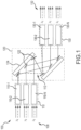
- FIG. 1 is a diagram illustrating an example of an optical circuit switch (OCS) 100, in accordance with one or more aspects of the subject technology.
- the OCS 100 is an all-optical switching matrix and includes input passive collimators 110 (e.g., 110-1, 110-2 ... 110-N), a mirror array 120, and output passive collimators 130 (e.g., 130-1, 130-2 ... 130-N).
- the input passive collimators 110 include multiple passive collimators that are coupled to a number N (e.g., in the range of about 128-1000) of optical fibers.
- Input light 108 enters the input passive collimators 110 through the optical fibers.
- the light transmitted through each optical fiber includes one or more optical wavelengths ( ⁇ i ).
- Output light 132 from the output passive collimators 130 is provided to a set of output optical fibers, each carrying light at the one or more optical wavelengths ( ⁇ i ).
- the collimators can be separate individual collimators or combined into a collimator array, as shown, for example, in FIG. 2A .
- the input and output passive collimators 110 and 130 are structurally similar and are described in more detail hereinafter.
- the mirror array 120 is a micro-electro-mechanical system (MEMS) based micro-mirror array that can selectively direct optical beams from individual optical fibers coupled to the input passive collimators 110 to selected optical fibers coupled to the output passive collimators 130.
- MEMS micro-electro-mechanical system
- the MEMS-based micro-mirror array (hereinafter "MEMS array") 120 includes two sets of micro-mirror arrays each having a number of micro-mirrors 122 formed on a substrate 124.
- the state of each micro-mirror 122 can be controlled by applying a voltage between two electrodes associated with each mirror in the MEMS array 120. For example, by rotating the mirrors in the MEMS array 120, light from any input fiber coupled to the input passive collimators 110 can be coupled to any output fiber coupled to the output passive collimators 130.
- the dotted-line path 112 is a result of potential beam pointing error that can be corrected by a control system that controls the position of the individual mirrors of the MEMS array 120.
- FIGs. 2A-2B are diagrams illustrating an example of an OCS collimator assembly 200A and an exploded view 200B of the same, in accordance with one or more aspects of the subject technology.
- the OCS collimator assembly 200A (hereinafter "collimator 200A") shown in FIG. 2A includes a collimator array 250, a mounting flange 240, and optical fibers 232.
- the flange 240 can be made of stainless steel, invar, or any other suitable material, and secures the collimator array 250 to the OCS assembly 200A. More detail of the collimator array 250 is shown in and described with respect to the exploded view 200B.
- the collimator array 250 includes an optical lens array 210, a spacer 220, a fiber array 230, a hole array 242, a first epoxy 212, and a second epoxy 222.
- an OCS such as the output collimators 130 shown in FIG. 1
- collimated input light beams enter from the free space to the optical lens array 210, and focused output light is coupled to the optical fibers 232 of the fiber array 230.
- the input collimators of the OCS such as the input collimators 110 shown in FIG.
- the optical lens array 210 is a two-dimensional (2-D) microlens array that includes a number of (e.g., 150 to 200) suitably-shaped micro-lenses (also referred to as "lenslets”), and can be about 15 ⁇ 15 mm 2 to 25x25 mm 2 .
- the optical lens array 210 is fabricated (e.g., via molding) using glass, for example, a high refractive index glass, which has a refractive index of 1.78 at 1550 run.
- the lenslets are spherical with an effective focal length of about 3.38 mm and identical radii of curvature of about 2.63 mm that vary by no more than 1% across the lenslets of the optical lens array. In some embodiments, other values of radii of curvature and effective focal length may be used.
- the high-index glass allows for spherical lenses to be used without significant insertion loss penalty due to spherical aberration.
- the lens surface figure error can be less than 200 nm. This precision fabrication can result in an improved fiber coupling efficiency and a low insertion loss (e.g., ⁇ 0.5 dB).
- optical lens array 210 is fabricated using a lens array mold that is micro-machined in a suitable material using a shaped (e.g., spherical) tip with a radius of curvature similar to the desired lens radius of curvature.
- the mold is re-machined in micron increments, and then re-measured after each machining attempt, to achieve the perfect (or near-perfect) spherical form of the lenslets to within ⁇ 200 nm.
- the mold can be used to make many (e.g., several thousand) lens arrays.
- the glass is molded at a suitable temperature and post-processed. The post-processing includes adding antireflection coatings to the lenses, and dicing the edges to the final desired dimensions.
- the spacer 220 can be a patterned spacer made of glass (e.g., Schott B33 glass) with surface dimensions matching the dimensions of the optical lens array 210 (e.g., ⁇ 20 ⁇ 20 mm) and a suitable thickness (e.g., 4 mm).
- the glass used for the spacer is selected for its refractive index to be well-matched (e.g., within less than 1%) to the doped core of the optical fibers (e.g., SMF28 type) of the fiber array 230.
- the spacer 220 includes a number of pads 224 made of a suitable material (e.g., silicon dioxide (SiO2) / chromium (Cr)).
- the pads 224 set an even and controlled separation gap between the optical lens array 210 and the spacer 220.
- the pads 224 are lithographically patterned on the edges (e.g. corners) of a first surface of the spacer 220. In some embodiments, the pads 224 have dimensions of about 5x1 mm x 5 um high.
- the material is deposited using chemical vapor deposition (CVD) or physical layer deposition (PLD) techniques known to persons of skill in the art to form a uniform thickness and are then etched to provide uniform height pads.
- the pads 224 can be created within the outer dimensions of the spacer 220 and optical lens array 210, but outside the clear aperture of the optical lens array 210, so as to not block the light propagating through the lenslets of the optical lens array 210.
- the spacer glass is precision polished to a thickness tolerance of approximately +/- 2 um.
- the first epoxy 212 is an optical path link-up epoxy and its refractive index is matched to the spacer 220 (within less than 2%) which is not part of the claimed invention.
- the first epoxy 212 couples the spacer 220 to the optical lens array 210.
- the second epoxy 222 couples the spacer 220 to the fiber array 230 with optical fibers that have a core refractive index of about 1.468 at 1550 nm.
- the collimator assembly 200A can be made of up to 176 optical fibers secured in the holes of the hole array 242 that collectively form the fiber array 230.
- the optical fibers 232 can be single-mode fibers (e.g., SMF28) that are assembled in the hole array (e.g., made of silicon, glass, or metal), such that the arrangement of the holes matches the geometrical arrangement of the lenses of the optical lens array 210 that in turn matches the geometrical arrangement of the MEMS array 120 of FIG. 1 .
- the collimator array 250 is attached to the mounting flange 240.
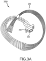
- FIGs. 3A through 3D are diagrams illustrating an example of a fiber collimator 300A, a front view 300B of the collimator array 250 included in the fiber collimator 300A, a molded glass optical lens array 300C, and light collimation through a molded glass lens 332 and a spacer 370, in accordance with one or more aspects of the subject technology.
- the fiber collimator 300A of FIG. 3A includes the optical fibers 232, the mounting flange 240 and a collimator array 250.
- the optical fibers 232 can be single mode such as SMF28 optical fibers and are assembled in the hole array discussed above and are attached to the mounting flange 240.
- the optical fibers 232 can be made of any desired length to suit an application in an all-optical or hybrid opto-electric network.
- the collimator array 250 includes the optical lens array 210, the spacer 220, the first and second epoxy 212 and 222, and the fiber array 230 mounted in the hole array 242, all shown in FIG. 2B , discussed above.
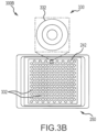
- the collimator array 250 shown in the front view 300B of FIG. 3B includes the optical lens array 210 coupled to the spacer (e.g., 220 of FIG. 2 ) using the first epoxy 212 and via the second epoxy 222 to the fiber array 230, which is in turn secured to the hole array 242.
- the optical lens array 210 as shown includes a number of (e.g., 176) lenslets 332.
- An example lenslet 332 is also shown in the exploded view 330. The lenslets 332 are aligned to the fibers of the fiber array 230.
- the alignment and attachment of the lens array 210 with the fiber array 230 is performed using an automated lens alignment robot having, for example, six degrees of freedom, 50 nm step size on the linear stages, and 7 urad step size on the rotation stages.
- the lens alignment robot can use a precision contact sensor to set a uniform gap height between a second (e.g., distal from the lens-array) surface of the spacer 220 and a first (e.g., proximal to the hole array) surface of the fiber array 230.
- the precision contact sensor can be used to co-planarize the two surfaces, and then set a constant 15 um gap height between them.
- the optical lens array 210 is aligned to the fiber array 230 using an optical feedback system based on measuring fiber coupling efficiency of a number of (e.g., 30-35) fibers in the upper and lower rows of the fiber array to improve the horizontal, vertical, and rotational alignment of the optical lens array 210 with respect to the fiber array 230.
- optical path link up epoxy e.g., epoxy 222 of FIG. 2B
- the 15 um bond line is re-set using the contact sensor, and the epoxy is UV cured and then thermally cured to complete the assembly.
- the collimator assembly e.g., 200A of FIG.
- the constant beam waist size and position at the center of an optical path across the mirror array of the OCS 100 of FIG. 1 provides improved fiber coupling efficiency and low insertion loss (e.g., ⁇ 0.5 dB) between the two collimators (e.g., 110 and 130 of FIG. 1 ) in the OCS 100 for all or nearly all possible port connections.
- the molded glass optical lens array 300C shown in FIG. 3C includes a number of (e.g., 176) suitably shaped lenslets 332 arranged in a 2-D array.
- the lenslets 332 are formed to protrude from a substrate 334.
- the 2-D lens array 300C is about 20x20 mm square and is fabricated in glass, which has a high refractive index (e.g., ⁇ 1.78 at 1550 nm).
- the lenslets 332 are spherical with identical radii of curvature (e.g., within 1%) of approximately 2.63mm and an effective focal length of approximately 3.38 mm.
- the radii of curvature and the effective focal length of the lenslets 332 can have other values.
- the high refractive index glass allows for spherical lenses to be used without significant insertion loss penalty due to spherical aberration.
- a measured lens surface figure error of ⁇ 200 nm is an indication of a precision fabrication, which results in the optimal fiber coupling efficiency and the substantially low insertion loss discussed below.
- the surface figure error is an integral value of errors between a desired (e.g., spherical) shape and the actual shape of a lens at a number of measured points on the surface of the lens.
- the surface figure error can be measured via interferometry using an interference microscope such as an optical profiler.
- FIG. 3D The light collimation through a spacer 370 and a molded glass lens 322 of the optical lens array 300C are shown in FIG. 3D .
- an optical light beam from an end-point 380 of a fiber 232 can be collimated through an optical path formed by a spacer 370 and the lenslet 332 coupled via an epoxy layer 335.
- the collimated light is a parallel beam that is reflected from a mirror 360 of a MEMS array (e.g., 120 shown in FIG. 1 )..
- the collimator 130 such as 130-1 of FIG.
- the light can be reflected from the mirror 360, then enter the lenslet 322 as a parallel beam and be focused, via the optical path through the lenslet 332, a first epoxy 335, the spacer 370, and a second epoxy 375 to the end-point 380 of the optical fiber 232.
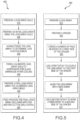
- FIG. 4 is a flow diagram illustrating an example method 400 of manufacturing the molded glass optical lens array of FIG. 3C , in accordance with one or more aspects of the subject technology.
- the method 400 begins with preparing the lens array mold (step 410).
- the lens array mold is micro-machined in a suitable material using a shaped (e.g., spherical) tip, having a radius of curvature similar to the desired lens radius of curvature.
- the mold is re-machined in micron increments, and then re-measured after each machining attempt, to achieve the perfect or near-perfect desired form of the lenslets, for example, to within ⁇ 200 nm.
- the glass is molded at a suitable temperature and the initial lens array is formed using the lens array mold (step 420).
- the lens position accuracy of the desired lens array e.g., 300C of FIG. 3C
- a desired position accuracy e.g., ⁇ +/- 1 um
- the mold is machined to compensate for the shrinkage of the glass when it cools.
- the formed initial lens array is characterized to determine a lens position error (step 430). In some embodiments, the characterization is performed using an automated alignment robot with 50 nm step size to determine the lens position error caused by the glass shrinkage.
- a calibrated lens array mold is prepared (e.g., by adjusting the mold or creating a new one) to compensate for glass shrinkage after cooling (step 440).
- the mold can be machined with an adjusted lens pitch that compensates for the glass shrinkage factor.
- measuring the lens array and then calibrating the mold for the glass shrinkage can be performed using available metrology tools such as a surface profilometer, with for example, an error of ⁇ 1um in 20 mm (0.005%).
- the final lens array is prepared using the calibrated lens array mold (step 450) and using a suitable high-index glass.
- the final lens array is then post processed (step 460).
- the post-processing includes adding AR coatings to the lenses as described above, and dicing the edges to the final desired dimensions.
- FIG.5 is a flow diagram illustrating an example method 500 of manufacturing the OCS collimator assembly 200A of FIG. 2A , in accordance with one or more aspects of the subject technology.
- the method 500 begins with preparing a lens array (step 510), for example, the lens array 300C of FIG. 3C , according to the method 400 described above with respect to FIG. 4 .
- the collimator assembly 200A also includes a spacer (e.g., 220 of FIG. 2B ), which is prepared (step 520) using a suitable glass (e.g., Schott B33) that is selected for its suitable refractive index (e.g., 1.456 at 1550 nm).
- a suitable glass e.g., Schott B33
- the spacer maintains a collimation distance between the optical lens array (e.g., 210 of FIG. 2B ) and the fiber array (e.g., 230 of FIG. 2B ) and enables control of the beam waist size and the beam waist location of the beam of the collimator assembly 200 of FIG. 2A .
- a number of pads are created on the spacer (step 530) by lithographically patterning a layer of a suitable material (e.g., SiO2 / Cr) on edges (e.g. corners) of a first side of the spacer.
- the pads are positioned within the outer dimensions of the spacer 220 and the optical lens array 210 of FIG. 2B , outside a clear aperture of the lens array, so that they do not block the light propagating through the lenslets.
- the spacer glass is precision polished to a thickness tolerance of approximately +/- 2 um.
- a layer of the first epoxy (e.g., 212 of FIG. 2B ) is used (step 540) to bond the lens spacer.
- the first epoxy 212 is index matched (to within less than 2%) to the spaced which is not part of the claimed invention.
- the first epoxy 212 has a refractive index value that is about halfway between a value of the refractive index of the spacer (e.g., about 1.456) and the refractive index of the glass material of the lens array (e.g., about 1.78).
- the spacer is placed in a tooling fixture, a controlled amount of the first epoxy is dispensed to the first side of the spacer, then the lens array is placed on the dispensed epoxy, and a weight is set on top of the tooling fixture to press the first epoxy between the lens array and the spacer.
- the epoxy is UV cured and then thermally cured to complete the attachment.
- the lens-spacer assembly is then aligned (at step 550) with the fiber array 230, as described above with respect to FIG. 3B , using an automated lens alignment robot having, for example, six degrees of freedom, 50 nm step size on the linear stages, and 7 urad step size on the rotation stages.
- the lens alignment robot can use a precision contact sensor to set a uniform gap height between the second surface of the spacer and the first surface of the fiber array 230.
- the precision contact sensor can be used to co-planarize the two surfaces, and then set a constant 15 um gap height between them.
- a second epoxy layer e.g., 224 of FIG. 2B
- FIG. 6 is a diagram illustrating an example chart 600 of return loss of the OCS collimator 200 of FIG. 2 , in accordance with one or more aspects of the subject technology.
- the chart 600 shows variation of return loss (RL, in dB) for a number of (e.g., 176) fibers (e.g., collimators such as 110-1 or 130-1 of FIG. 1 ) of the collimators 110 or 130 of FIG. 1 , each unit including an optical path between a lenslet of the optical lens array 210 and a respective optical fiber of the fiber array 230 shown in FIG. 2B .
- RL return loss
- the plots 610, 620, 630 and 640 respectively correspond to average RL values for light in the O-band (1270-1360 nm) and CL-band (1530-1620 nm) and minimum RL values for the light in the O-band and the CL-band.
- the collimator of the subject technology uses the second epoxy (e.g., 222 of FIG. 2 ) having an epoxy refractive index for reduced return loss at the optical fiber interface, and an anti-reflection (AR) coating on the piano side of the lens array which is not part of the claimed invention
- the fiber array is made of SMF28 Ultra fiber with a refractive index of 1.468 at 1550 nm, while the lens array is made of a glass with a refractive index of 1.78 at 1550 nm.
- the fiber array 230 and the optical lens array 210 are separated by a glass spacer that positions the lens array at the required distance from the fiber array for beam collimation, and also provides a refractive index matching solution.
- the spacer is made of Schott B33 glass with a refractive index of 1.456 at 1550 nm.
- the second epoxy has a refractive index of 1.462 that is almost halfway between the refractive index of the spacer (e.g., about 1.456) and the refractive index of the optical core of the optical fiber (e.g., about 1.468) and can reduce the return loss at the spacer-fiber interface.
- the disclosed collimator utilizes an AR coating designed for the lens substrate (e.g., 334 of FIG. 3 ) at the lens-spacer interface that is selected to reduce return loss from constructive interference in the spacer layer.
- the fiber coupling efficiency of a reflection from the lens-epoxy-spacer interface back into the fiber is approximately -32.4dB. This is added to the Fresnel reflectance to produce the total return loss from this interface.
- the collimator return loss is characterized by sweeping a tunable laser from 1270 to 1360 nm (O-band) or 1530-1620 nm (CL-band) with 10 pm resolution, and measuring the return loss oscillations. Then, the average and minimum RL values over the O-band and CL-band for each optical fiber are determined, as shown in the plots 610, 620, 630, and 640. In some embodiments, the fiber ports that do not meet the return loss specifications can be eliminated. In one or more embodiments, an optical backscatter reflectometer is used to spatially locate regions of higher return loss in the collimator.
- FIG. 7 is a diagram illustrating an example chart 700 of return loss of the OCS collimator of FIG. 2 , with and without an anti-reflection (AR) coating.
- the chart 700 includes plots 710 and 720 corresponding to lenses with and without AR coating.
- the return loss values are given in dB and for a number of wavelengths in the O-band.
- Measurement results show that there is a slow return loss oscillation due to constructive interference in the epoxy layer, with a period of 38 nm that is set by the 15um thickness of the epoxy layer. There is also a fast return loss oscillation due to constructive interference in the spacer layer, with a period of 0.11 nm (as shown for fast oscillations of plot 720) that is determined by the thickness of the spacer (in this example 4.146 mm). These oscillations are superimposed.
- references to "or” may be construed as inclusive so that any terms described using “or” may indicate any of a single, more than one, and all of the described terms.
- the labels “first,” “second,” “third,” and so forth are not necessarily meant to indicate an ordering and are generally used merely to distinguish between like or similar items or elements.
- particular implementations of the subject matter have been described.
- Other implementations are within the scope of the following claims.
- the actions recited in the claims can be performed in a different order and still achieve desirable results.
- the processes depicted in the accompanying figures do not necessarily require the particular order shown, or sequential order, to achieve desirable results.
- multitasking or parallel processing may be used.
- a collimator device includes a fiber array including multiple optical fibers disposed in a hole array.
- An optical lens array is aligned and coupled to the fiber array.
- a spacer is disposed between the fiber array and the optical lens array and provides substantially uniform spacing between lenses in the optical lens array and corresponding fibers in the fiber array.
- Multiple pads are positioned along edges of a surface of the spacer facing the optical lens array defining a first separation gap between the spacer and the optical lens array.
- a first epoxy bonds the spacer to the optical lens array, and a second epoxy bonds the spacer to the fiber array.
- the optical lens array includes a glass substrate having a first surface defining lenses in a two-dimensional array.
Landscapes
- Physics & Mathematics (AREA)
- General Physics & Mathematics (AREA)
- Optics & Photonics (AREA)
- Optical Couplings Of Light Guides (AREA)
- Mechanical Light Control Or Optical Switches (AREA)
Applications Claiming Priority (1)
| Application Number | Priority Date | Filing Date | Title |
|---|---|---|---|
| US15/266,655 US9726824B1 (en) | 2016-09-15 | 2016-09-15 | Optical circuit switch collimator |
Publications (3)
| Publication Number | Publication Date |
|---|---|
| EP3306366A2 EP3306366A2 (en) | 2018-04-11 |
| EP3306366A3 EP3306366A3 (en) | 2018-06-13 |
| EP3306366B1 true EP3306366B1 (en) | 2023-06-07 |
Family
ID=59410692
Family Applications (1)
| Application Number | Title | Priority Date | Filing Date |
|---|---|---|---|
| EP17191030.0A Active EP3306366B1 (en) | 2016-09-15 | 2017-09-14 | Optical circuit switch collimator |
Country Status (10)
| Country | Link |
|---|---|
| US (1) | US9726824B1 (enExample) |
| EP (1) | EP3306366B1 (enExample) |
| JP (1) | JP6338756B2 (enExample) |
| CN (1) | CN107831568A (enExample) |
| DE (1) | DE202017105560U1 (enExample) |
| DK (1) | DK3306366T3 (enExample) |
| FI (1) | FI3306366T3 (enExample) |
| HK (1) | HK1251664A1 (enExample) |
| SG (1) | SG10201707299YA (enExample) |
| TW (1) | TWI750206B (enExample) |
Families Citing this family (12)
| Publication number | Priority date | Publication date | Assignee | Title |
|---|---|---|---|---|
| US9846280B2 (en) * | 2016-01-29 | 2017-12-19 | Ii-Vi Incorporated | Monolithic two-dimensional optical fiber array |
| WO2018229992A1 (ja) * | 2017-06-16 | 2018-12-20 | 京セラ株式会社 | 光コネクタモジュール |
| CN110618485A (zh) * | 2018-06-20 | 2019-12-27 | 富晋精密工业(晋城)有限公司 | 光纤阵列装置 |
| WO2020025438A1 (en) | 2018-07-30 | 2020-02-06 | Schleifring Gmbh | Device and method for welding of glass fibers to a micro lens array to manufacture a fiber collimator array |
| US10754070B2 (en) | 2018-12-05 | 2020-08-25 | International Business Machines Corporation | Microlens array assembling process |
| CN113227861B (zh) * | 2018-12-26 | 2022-11-11 | 华为技术有限公司 | 具有硅透镜的多通道模式转换器 |
| US10690867B1 (en) | 2019-02-12 | 2020-06-23 | International Business Machines Corporation | Optical device with adhesive connection of recess or side protrusion |
| EP4369113B1 (fr) * | 2019-12-23 | 2025-10-01 | Blancpain SA | Mecanisme d'affichage des phases de lune |
| EP3842874B1 (fr) * | 2019-12-23 | 2023-09-20 | Blancpain SA | Dispositif optique permettant de creer des effets optiques esthetiques et techniques |
| US11561345B2 (en) * | 2020-02-14 | 2023-01-24 | Google Llc | Apertures for reduced dynamic crosstalk and stray light control |
| US11630265B2 (en) * | 2020-04-15 | 2023-04-18 | Google Llc | Glass fiber hole plates for 2D fiber collimators and methods for alignment and fabrication for optical switching applications |
| CN116203728A (zh) | 2023-01-06 | 2023-06-02 | 立讯精密科技(南京)有限公司 | 增强现实显示系统及增强现实显示设备 |
Family Cites Families (36)
| Publication number | Priority date | Publication date | Assignee | Title |
|---|---|---|---|---|
| US5077622A (en) | 1990-05-31 | 1991-12-31 | The United States Of America As Represented By The Administrator Of The National Aeronautics And Space Administration | Apparatus for precision focussing and positioning of a beam waist on a target |
| JPH07318860A (ja) | 1994-05-27 | 1995-12-08 | Kyocera Corp | 光アイソレータ |
| JPH08152581A (ja) | 1994-11-29 | 1996-06-11 | Nippon Telegr & Teleph Corp <Ntt> | コリメータおよびコリメータアレイ |
| JPH0990159A (ja) * | 1995-09-28 | 1997-04-04 | Furukawa Electric Co Ltd:The | 光モジュール及びその組立方法 |
| KR100248058B1 (ko) * | 1997-08-27 | 2000-03-15 | 윤종용 | 금속 증착된 광섬유 어레이 모듈 |
| WO2000039626A1 (en) * | 1998-12-31 | 2000-07-06 | Optical Coating Laboratory, Inc. | Wavelength selective optical switch |
| JP2000231028A (ja) * | 1999-02-09 | 2000-08-22 | Shinko Electric Ind Co Ltd | 光径変換伝送路 |
| JP2001305376A (ja) | 2000-02-17 | 2001-10-31 | Nippon Sheet Glass Co Ltd | コリメータアレイ装置の設計方法及びこの方法によって作製されたコリメータアレイ装置 |
| US6483071B1 (en) | 2000-05-16 | 2002-11-19 | General Scanning Inc. | Method and system for precisely positioning a waist of a material-processing laser beam to process microstructures within a laser-processing site |
| US6483961B1 (en) * | 2000-06-02 | 2002-11-19 | Calient Networks, Inc. | Dual refraction index collimator for an optical switch |
| US6470123B1 (en) * | 2000-07-18 | 2002-10-22 | Fiberguide Industries, Inc. | Large optical fiber array assembly and method |
| EP1305656A4 (en) * | 2000-07-31 | 2006-03-08 | Rochester Photonics Corp | STRUCTURED UMBRELLAS FOR REGULATED DIFFUSION OF LIGHT |
| US20020076151A1 (en) * | 2000-12-18 | 2002-06-20 | Kinard William Brian | Optical collimator device utilizing an integrated lens/spacer element |
| US20020126381A1 (en) * | 2001-03-05 | 2002-09-12 | Suh Seong Woo | Stacks of optical structures and methods and apparatus for making same |
| US6587618B2 (en) * | 2001-03-16 | 2003-07-01 | Corning Incorporated | Collimator array and method and system for aligning optical fibers to a lens array |
| US6597510B2 (en) | 2001-11-02 | 2003-07-22 | Corning Incorporated | Methods and apparatus for making optical devices including microlens arrays |
| JP4313987B2 (ja) * | 2002-06-18 | 2009-08-12 | 富士通株式会社 | ファイバブロックの製造方法 |
| US6950570B1 (en) * | 2002-08-13 | 2005-09-27 | Active Optical Networks, Inc. | Integrated fiber, sensor and lens arrays for optical networks |
| JP2004101847A (ja) * | 2002-09-09 | 2004-04-02 | Nippon Sheet Glass Co Ltd | 光モジュール |
| JP2004102108A (ja) * | 2002-09-12 | 2004-04-02 | Fujitsu Ltd | コリメータアレイ及び該コリメータアレイを備えた光デバイス |
| JP2004252244A (ja) * | 2003-02-21 | 2004-09-09 | Nippon Telegr & Teleph Corp <Ntt> | 光ファイバコリメータアレイ |
| JP2006126566A (ja) * | 2004-10-29 | 2006-05-18 | Fujitsu Ltd | コリメータアレイ及びその製造方法 |
| KR100669142B1 (ko) * | 2005-04-20 | 2007-01-15 | (주)더리즈 | 발광 소자와 이의 제조 방법 |
| US7295375B2 (en) | 2005-08-02 | 2007-11-13 | International Business Machines Corporation | Injection molded microlenses for optical interconnects |
| US8393804B2 (en) * | 2006-06-19 | 2013-03-12 | Commscope, Inc. Of North Carolina | Expanded beam connector concepts |
| JP5133595B2 (ja) * | 2007-05-15 | 2013-01-30 | オリンパスメディカルシステムズ株式会社 | 照明光検出用光学系並びにそれを備えた光学装置及び内視鏡装置 |
| JP4915385B2 (ja) * | 2008-04-11 | 2012-04-11 | 富士通株式会社 | ファイバコリメータアレイ、波長選択スイッチ、光学部品及びファイバコリメータアレイの製造方法 |
| DE102008001653A1 (de) * | 2008-05-08 | 2009-12-03 | Schleifring Und Apparatebau Gmbh | Linsenanordnung für optische Drehübertrager |
| CN101408647B (zh) | 2008-11-25 | 2011-01-12 | 中国科学院上海微系统与信息技术研究所 | 一种基于双光纤椭圆光斑准直器的2×2mems光开关 |
| JP5138656B2 (ja) * | 2009-10-15 | 2013-02-06 | シャープ株式会社 | レンズ評価方法 |
| JP2011197633A (ja) * | 2010-02-23 | 2011-10-06 | Furukawa Electric Co Ltd:The | 光導波路コリメータおよび光スイッチ装置 |
| CN103874947B (zh) * | 2011-07-29 | 2017-05-10 | 莫列斯公司 | 光纤组件和制造该光纤组件的方法 |
| JP5981145B2 (ja) * | 2012-01-07 | 2016-08-31 | 古河電気工業株式会社 | 回路基板および通信システム |
| US9063313B1 (en) * | 2012-07-06 | 2015-06-23 | Compass Electro Optical System Ltd. | Fiber coupling using collimated beams |
| US9529155B2 (en) * | 2012-11-28 | 2016-12-27 | Corning Optical Communications LLC | Gradient index (GRIN) lens chips and associated small form factor optical arrays for optical connections, related fiber optic connectors |
| CN103926656A (zh) * | 2014-04-21 | 2014-07-16 | 深圳市天阳谷科技发展有限公司 | 一种光纤准直器 |
-
2016
- 2016-09-15 US US15/266,655 patent/US9726824B1/en active Active
-
2017
- 2017-08-03 TW TW106126168A patent/TWI750206B/zh active
- 2017-08-31 CN CN201710769765.5A patent/CN107831568A/zh active Pending
- 2017-09-07 SG SG10201707299YA patent/SG10201707299YA/en unknown
- 2017-09-14 DE DE202017105560.4U patent/DE202017105560U1/de active Active
- 2017-09-14 FI FIEP17191030.0T patent/FI3306366T3/fi active
- 2017-09-14 EP EP17191030.0A patent/EP3306366B1/en active Active
- 2017-09-14 DK DK17191030.0T patent/DK3306366T3/da active
- 2017-09-14 JP JP2017176997A patent/JP6338756B2/ja active Active
-
2018
- 2018-08-22 HK HK18110808.1A patent/HK1251664A1/zh unknown
Also Published As
| Publication number | Publication date |
|---|---|
| JP2018045240A (ja) | 2018-03-22 |
| TWI750206B (zh) | 2021-12-21 |
| EP3306366A2 (en) | 2018-04-11 |
| TW201814342A (zh) | 2018-04-16 |
| SG10201707299YA (en) | 2018-04-27 |
| US9726824B1 (en) | 2017-08-08 |
| EP3306366A3 (en) | 2018-06-13 |
| DK3306366T3 (da) | 2023-09-11 |
| HK1251664A1 (zh) | 2019-02-01 |
| JP6338756B2 (ja) | 2018-06-06 |
| CN107831568A (zh) | 2018-03-23 |
| DE202017105560U1 (de) | 2017-12-19 |
| FI3306366T3 (fi) | 2023-10-19 |
Similar Documents
| Publication | Publication Date | Title |
|---|---|---|
| EP3306366B1 (en) | Optical circuit switch collimator | |
| US20090232450A1 (en) | Simple fiber optic cavity | |
| US6577793B2 (en) | Optical switch | |
| US7054077B2 (en) | Method for constructing a catadioptric lens system | |
| US20030228100A1 (en) | Fiber collimator array | |
| Mellette et al. | A scalable, partially configurable optical switch for data center networks | |
| EP3182180B1 (en) | Multichannel fiber optic rotary joint(forj) having an achromatic metasurface | |
| US20030231829A1 (en) | Lens array for use with array of fibers | |
| EP2359108B1 (en) | Mirror structure | |
| CN109298504A (zh) | 微机电光学波长参考标准具 | |
| US6934087B1 (en) | Fiber optic collimator and collimator array | |
| Wu et al. | Design and use of compact lensed fibers for low cost packaging of optical MEMS components | |
| KR101718481B1 (ko) | 볼렌즈 기반의 확장 빔 커넥터 | |
| Fernandez et al. | Modular MEMS design and fabrication for an 80 x 80 transparent optical cross-connect switch | |
| Mita et al. | An out-of-plane polysilicon actuator with a smooth vertical mirror for optical fiber switch application | |
| US20090060415A1 (en) | Fiber optic cavity | |
| Chen et al. | Microjet printing of high-precision microlens array for packaging of fiber optic components | |
| US20050013539A1 (en) | Optical coupling system | |
| JP2003185873A (ja) | 二次元光学部材アレイ及び二次元導波路装置並びにそれらの製造方法 | |
| WO2002056076A2 (en) | Fiber optic collimator array | |
| US11656411B2 (en) | Monolithic fiber-lens array for communication and remote sensing | |
| Jain | High accuracy precision microlens arrays: Precision glass molding offers maximum manufacturing reproducibility and design accuracy | |
| Liu et al. | Design and fabrication of a coherent array of single-mode optical fibers for the nulling coronagraph | |
| Baehr et al. | Applications and potential of the mask structured ion exchange technique (MSI) in micro-optics | |
| JP2004070310A (ja) | 光デバイスユニット、光デバイス及びマイクロレンズアレイ |
Legal Events
| Date | Code | Title | Description |
|---|---|---|---|
| PUAI | Public reference made under article 153(3) epc to a published international application that has entered the european phase |
Free format text: ORIGINAL CODE: 0009012 |
|
| STAA | Information on the status of an ep patent application or granted ep patent |
Free format text: STATUS: THE APPLICATION HAS BEEN PUBLISHED |
|
| AK | Designated contracting states |
Kind code of ref document: A2 Designated state(s): AL AT BE BG CH CY CZ DE DK EE ES FI FR GB GR HR HU IE IS IT LI LT LU LV MC MK MT NL NO PL PT RO RS SE SI SK SM TR |
|
| AX | Request for extension of the european patent |
Extension state: BA ME |
|
| PUAL | Search report despatched |
Free format text: ORIGINAL CODE: 0009013 |
|
| AK | Designated contracting states |
Kind code of ref document: A3 Designated state(s): AL AT BE BG CH CY CZ DE DK EE ES FI FR GB GR HR HU IE IS IT LI LT LU LV MC MK MT NL NO PL PT RO RS SE SI SK SM TR |
|
| AX | Request for extension of the european patent |
Extension state: BA ME |
|
| RIC1 | Information provided on ipc code assigned before grant |
Ipc: G02B 6/32 20060101ALI20180509BHEP Ipc: G02B 6/35 20060101AFI20180509BHEP |
|
| STAA | Information on the status of an ep patent application or granted ep patent |
Free format text: STATUS: REQUEST FOR EXAMINATION WAS MADE |
|
| 17P | Request for examination filed |
Effective date: 20181213 |
|
| RBV | Designated contracting states (corrected) |
Designated state(s): AL AT BE BG CH CY CZ DE DK EE ES FI FR GB GR HR HU IE IS IT LI LT LU LV MC MK MT NL NO PL PT RO RS SE SI SK SM TR |
|
| STAA | Information on the status of an ep patent application or granted ep patent |
Free format text: STATUS: EXAMINATION IS IN PROGRESS |
|
| 17Q | First examination report despatched |
Effective date: 20200616 |
|
| GRAP | Despatch of communication of intention to grant a patent |
Free format text: ORIGINAL CODE: EPIDOSNIGR1 |
|
| STAA | Information on the status of an ep patent application or granted ep patent |
Free format text: STATUS: GRANT OF PATENT IS INTENDED |
|
| INTG | Intention to grant announced |
Effective date: 20230102 |
|
| GRAS | Grant fee paid |
Free format text: ORIGINAL CODE: EPIDOSNIGR3 |
|
| GRAA | (expected) grant |
Free format text: ORIGINAL CODE: 0009210 |
|
| STAA | Information on the status of an ep patent application or granted ep patent |
Free format text: STATUS: THE PATENT HAS BEEN GRANTED |
|
| AK | Designated contracting states |
Kind code of ref document: B1 Designated state(s): AL AT BE BG CH CY CZ DE DK EE ES FI FR GB GR HR HU IE IS IT LI LT LU LV MC MK MT NL NO PL PT RO RS SE SI SK SM TR |
|
| REG | Reference to a national code |
Ref country code: GB Ref legal event code: FG4D |
|
| REG | Reference to a national code |
Ref country code: CH Ref legal event code: EP Ref country code: AT Ref legal event code: REF Ref document number: 1576823 Country of ref document: AT Kind code of ref document: T Effective date: 20230615 |
|
| REG | Reference to a national code |
Ref country code: DE Ref legal event code: R096 Ref document number: 602017069379 Country of ref document: DE |
|
| REG | Reference to a national code |
Ref country code: DK Ref legal event code: T3 Effective date: 20230908 |
|
| REG | Reference to a national code |
Ref country code: NL Ref legal event code: FP |
|
| REG | Reference to a national code |
Ref country code: LT Ref legal event code: MG9D |
|
| REG | Reference to a national code |
Ref country code: SE Ref legal event code: TRGR |
|
| REG | Reference to a national code |
Ref country code: FI Ref legal event code: FGE |
|
| PG25 | Lapsed in a contracting state [announced via postgrant information from national office to epo] |
Ref country code: NO Free format text: LAPSE BECAUSE OF FAILURE TO SUBMIT A TRANSLATION OF THE DESCRIPTION OR TO PAY THE FEE WITHIN THE PRESCRIBED TIME-LIMIT Effective date: 20230907 Ref country code: ES Free format text: LAPSE BECAUSE OF FAILURE TO SUBMIT A TRANSLATION OF THE DESCRIPTION OR TO PAY THE FEE WITHIN THE PRESCRIBED TIME-LIMIT Effective date: 20230607 |
|
| REG | Reference to a national code |
Ref country code: AT Ref legal event code: MK05 Ref document number: 1576823 Country of ref document: AT Kind code of ref document: T Effective date: 20230607 |
|
| PG25 | Lapsed in a contracting state [announced via postgrant information from national office to epo] |
Ref country code: RS Free format text: LAPSE BECAUSE OF FAILURE TO SUBMIT A TRANSLATION OF THE DESCRIPTION OR TO PAY THE FEE WITHIN THE PRESCRIBED TIME-LIMIT Effective date: 20230607 Ref country code: LV Free format text: LAPSE BECAUSE OF FAILURE TO SUBMIT A TRANSLATION OF THE DESCRIPTION OR TO PAY THE FEE WITHIN THE PRESCRIBED TIME-LIMIT Effective date: 20230607 Ref country code: LT Free format text: LAPSE BECAUSE OF FAILURE TO SUBMIT A TRANSLATION OF THE DESCRIPTION OR TO PAY THE FEE WITHIN THE PRESCRIBED TIME-LIMIT Effective date: 20230607 Ref country code: HR Free format text: LAPSE BECAUSE OF FAILURE TO SUBMIT A TRANSLATION OF THE DESCRIPTION OR TO PAY THE FEE WITHIN THE PRESCRIBED TIME-LIMIT Effective date: 20230607 Ref country code: GR Free format text: LAPSE BECAUSE OF FAILURE TO SUBMIT A TRANSLATION OF THE DESCRIPTION OR TO PAY THE FEE WITHIN THE PRESCRIBED TIME-LIMIT Effective date: 20230908 |
|
| PG25 | Lapsed in a contracting state [announced via postgrant information from national office to epo] |
Ref country code: FI Free format text: LAPSE BECAUSE OF FAILURE TO SUBMIT A TRANSLATION OF THE DESCRIPTION OR TO PAY THE FEE WITHIN THE PRESCRIBED TIME-LIMIT Effective date: 20230607 |
|
| PG25 | Lapsed in a contracting state [announced via postgrant information from national office to epo] |
Ref country code: SK Free format text: LAPSE BECAUSE OF FAILURE TO SUBMIT A TRANSLATION OF THE DESCRIPTION OR TO PAY THE FEE WITHIN THE PRESCRIBED TIME-LIMIT Effective date: 20230607 |
|
| PG25 | Lapsed in a contracting state [announced via postgrant information from national office to epo] |
Ref country code: IS Free format text: LAPSE BECAUSE OF FAILURE TO SUBMIT A TRANSLATION OF THE DESCRIPTION OR TO PAY THE FEE WITHIN THE PRESCRIBED TIME-LIMIT Effective date: 20231007 |
|
| PG25 | Lapsed in a contracting state [announced via postgrant information from national office to epo] |
Ref country code: SM Free format text: LAPSE BECAUSE OF FAILURE TO SUBMIT A TRANSLATION OF THE DESCRIPTION OR TO PAY THE FEE WITHIN THE PRESCRIBED TIME-LIMIT Effective date: 20230607 Ref country code: SK Free format text: LAPSE BECAUSE OF FAILURE TO SUBMIT A TRANSLATION OF THE DESCRIPTION OR TO PAY THE FEE WITHIN THE PRESCRIBED TIME-LIMIT Effective date: 20230607 Ref country code: RO Free format text: LAPSE BECAUSE OF FAILURE TO SUBMIT A TRANSLATION OF THE DESCRIPTION OR TO PAY THE FEE WITHIN THE PRESCRIBED TIME-LIMIT Effective date: 20230607 Ref country code: PT Free format text: LAPSE BECAUSE OF FAILURE TO SUBMIT A TRANSLATION OF THE DESCRIPTION OR TO PAY THE FEE WITHIN THE PRESCRIBED TIME-LIMIT Effective date: 20231009 Ref country code: IS Free format text: LAPSE BECAUSE OF FAILURE TO SUBMIT A TRANSLATION OF THE DESCRIPTION OR TO PAY THE FEE WITHIN THE PRESCRIBED TIME-LIMIT Effective date: 20231007 Ref country code: EE Free format text: LAPSE BECAUSE OF FAILURE TO SUBMIT A TRANSLATION OF THE DESCRIPTION OR TO PAY THE FEE WITHIN THE PRESCRIBED TIME-LIMIT Effective date: 20230607 Ref country code: CZ Free format text: LAPSE BECAUSE OF FAILURE TO SUBMIT A TRANSLATION OF THE DESCRIPTION OR TO PAY THE FEE WITHIN THE PRESCRIBED TIME-LIMIT Effective date: 20230607 Ref country code: AT Free format text: LAPSE BECAUSE OF FAILURE TO SUBMIT A TRANSLATION OF THE DESCRIPTION OR TO PAY THE FEE WITHIN THE PRESCRIBED TIME-LIMIT Effective date: 20230607 |
|
| PG25 | Lapsed in a contracting state [announced via postgrant information from national office to epo] |
Ref country code: PL Free format text: LAPSE BECAUSE OF FAILURE TO SUBMIT A TRANSLATION OF THE DESCRIPTION OR TO PAY THE FEE WITHIN THE PRESCRIBED TIME-LIMIT Effective date: 20230607 |
|
| REG | Reference to a national code |
Ref country code: DE Ref legal event code: R097 Ref document number: 602017069379 Country of ref document: DE |
|
| PLBE | No opposition filed within time limit |
Free format text: ORIGINAL CODE: 0009261 |
|
| STAA | Information on the status of an ep patent application or granted ep patent |
Free format text: STATUS: NO OPPOSITION FILED WITHIN TIME LIMIT |
|
| PG25 | Lapsed in a contracting state [announced via postgrant information from national office to epo] |
Ref country code: SI Free format text: LAPSE BECAUSE OF FAILURE TO SUBMIT A TRANSLATION OF THE DESCRIPTION OR TO PAY THE FEE WITHIN THE PRESCRIBED TIME-LIMIT Effective date: 20230607 |
|
| 26N | No opposition filed |
Effective date: 20240308 |
|
| PG25 | Lapsed in a contracting state [announced via postgrant information from national office to epo] |
Ref country code: LU Free format text: LAPSE BECAUSE OF NON-PAYMENT OF DUE FEES Effective date: 20230914 |
|
| PG25 | Lapsed in a contracting state [announced via postgrant information from national office to epo] |
Ref country code: SI Free format text: LAPSE BECAUSE OF FAILURE TO SUBMIT A TRANSLATION OF THE DESCRIPTION OR TO PAY THE FEE WITHIN THE PRESCRIBED TIME-LIMIT Effective date: 20230607 Ref country code: LU Free format text: LAPSE BECAUSE OF NON-PAYMENT OF DUE FEES Effective date: 20230914 Ref country code: IT Free format text: LAPSE BECAUSE OF FAILURE TO SUBMIT A TRANSLATION OF THE DESCRIPTION OR TO PAY THE FEE WITHIN THE PRESCRIBED TIME-LIMIT Effective date: 20230607 Ref country code: MC Free format text: LAPSE BECAUSE OF FAILURE TO SUBMIT A TRANSLATION OF THE DESCRIPTION OR TO PAY THE FEE WITHIN THE PRESCRIBED TIME-LIMIT Effective date: 20230607 |
|
| PG25 | Lapsed in a contracting state [announced via postgrant information from national office to epo] |
Ref country code: BG Free format text: LAPSE BECAUSE OF FAILURE TO SUBMIT A TRANSLATION OF THE DESCRIPTION OR TO PAY THE FEE WITHIN THE PRESCRIBED TIME-LIMIT Effective date: 20230607 |
|
| PG25 | Lapsed in a contracting state [announced via postgrant information from national office to epo] |
Ref country code: BG Free format text: LAPSE BECAUSE OF FAILURE TO SUBMIT A TRANSLATION OF THE DESCRIPTION OR TO PAY THE FEE WITHIN THE PRESCRIBED TIME-LIMIT Effective date: 20230607 |
|
| PG2D | Information on lapse in contracting state deleted |
Ref country code: FI |
|
| PG25 | Lapsed in a contracting state [announced via postgrant information from national office to epo] |
Ref country code: CY Free format text: LAPSE BECAUSE OF FAILURE TO SUBMIT A TRANSLATION OF THE DESCRIPTION OR TO PAY THE FEE WITHIN THE PRESCRIBED TIME-LIMIT; INVALID AB INITIO Effective date: 20170914 |
|
| PG25 | Lapsed in a contracting state [announced via postgrant information from national office to epo] |
Ref country code: HU Free format text: LAPSE BECAUSE OF FAILURE TO SUBMIT A TRANSLATION OF THE DESCRIPTION OR TO PAY THE FEE WITHIN THE PRESCRIBED TIME-LIMIT; INVALID AB INITIO Effective date: 20170914 |
|
| REG | Reference to a national code |
Ref country code: CH Ref legal event code: U11 Free format text: ST27 STATUS EVENT CODE: U-0-0-U10-U11 (AS PROVIDED BY THE NATIONAL OFFICE) Effective date: 20251001 |
|
| PGFP | Annual fee paid to national office [announced via postgrant information from national office to epo] |
Ref country code: FI Payment date: 20250925 Year of fee payment: 9 |
|
| PGFP | Annual fee paid to national office [announced via postgrant information from national office to epo] |
Ref country code: DE Payment date: 20250929 Year of fee payment: 9 Ref country code: DK Payment date: 20250925 Year of fee payment: 9 |
|
| PGFP | Annual fee paid to national office [announced via postgrant information from national office to epo] |
Ref country code: NL Payment date: 20250926 Year of fee payment: 9 |
|
| PGFP | Annual fee paid to national office [announced via postgrant information from national office to epo] |
Ref country code: BE Payment date: 20250929 Year of fee payment: 9 Ref country code: GB Payment date: 20250929 Year of fee payment: 9 |
|
| PGFP | Annual fee paid to national office [announced via postgrant information from national office to epo] |
Ref country code: FR Payment date: 20250925 Year of fee payment: 9 |
|
| PGFP | Annual fee paid to national office [announced via postgrant information from national office to epo] |
Ref country code: SE Payment date: 20250927 Year of fee payment: 9 |
|
| PGFP | Annual fee paid to national office [announced via postgrant information from national office to epo] |
Ref country code: IE Payment date: 20250929 Year of fee payment: 9 |
|
| PG25 | Lapsed in a contracting state [announced via postgrant information from national office to epo] |
Ref country code: TR Free format text: LAPSE BECAUSE OF FAILURE TO SUBMIT A TRANSLATION OF THE DESCRIPTION OR TO PAY THE FEE WITHIN THE PRESCRIBED TIME-LIMIT Effective date: 20230607 |
|
| PGFP | Annual fee paid to national office [announced via postgrant information from national office to epo] |
Ref country code: CH Payment date: 20251001 Year of fee payment: 9 |