EP3285152B1 - Berührungssteuerungsanzeigevorrichtung mit hochresistenter schicht - Google Patents
Berührungssteuerungsanzeigevorrichtung mit hochresistenter schicht Download PDFInfo
- Publication number
- EP3285152B1 EP3285152B1 EP16856923.4A EP16856923A EP3285152B1 EP 3285152 B1 EP3285152 B1 EP 3285152B1 EP 16856923 A EP16856923 A EP 16856923A EP 3285152 B1 EP3285152 B1 EP 3285152B1
- Authority
- EP
- European Patent Office
- Prior art keywords
- high resistivity
- layer
- color filter
- filter substrate
- resistivity layer
- Prior art date
- Legal status (The legal status is an assumption and is not a legal conclusion. Google has not performed a legal analysis and makes no representation as to the accuracy of the status listed.)
- Active
Links
Images


Classifications
-
- G—PHYSICS
- G02—OPTICS
- G02F—OPTICAL DEVICES OR ARRANGEMENTS FOR THE CONTROL OF LIGHT BY MODIFICATION OF THE OPTICAL PROPERTIES OF THE MEDIA OF THE ELEMENTS INVOLVED THEREIN; NON-LINEAR OPTICS; FREQUENCY-CHANGING OF LIGHT; OPTICAL LOGIC ELEMENTS; OPTICAL ANALOGUE/DIGITAL CONVERTERS
- G02F1/00—Devices or arrangements for the control of the intensity, colour, phase, polarisation or direction of light arriving from an independent light source, e.g. switching, gating or modulating; Non-linear optics
- G02F1/01—Devices or arrangements for the control of the intensity, colour, phase, polarisation or direction of light arriving from an independent light source, e.g. switching, gating or modulating; Non-linear optics for the control of the intensity, phase, polarisation or colour
- G02F1/13—Devices or arrangements for the control of the intensity, colour, phase, polarisation or direction of light arriving from an independent light source, e.g. switching, gating or modulating; Non-linear optics for the control of the intensity, phase, polarisation or colour based on liquid crystals, e.g. single liquid crystal display cells
- G02F1/133—Constructional arrangements; Operation of liquid crystal cells; Circuit arrangements
- G02F1/1333—Constructional arrangements; Manufacturing methods
- G02F1/13338—Input devices, e.g. touch panels
-
- G—PHYSICS
- G06—COMPUTING OR CALCULATING; COUNTING
- G06F—ELECTRIC DIGITAL DATA PROCESSING
- G06F3/00—Input arrangements for transferring data to be processed into a form capable of being handled by the computer; Output arrangements for transferring data from processing unit to output unit, e.g. interface arrangements
- G06F3/01—Input arrangements or combined input and output arrangements for interaction between user and computer
- G06F3/03—Arrangements for converting the position or the displacement of a member into a coded form
- G06F3/041—Digitisers, e.g. for touch screens or touch pads, characterised by the transducing means
- G06F3/0412—Digitisers structurally integrated in a display
-
- H—ELECTRICITY
- H10—SEMICONDUCTOR DEVICES; ELECTRIC SOLID-STATE DEVICES NOT OTHERWISE PROVIDED FOR
- H10D—INORGANIC ELECTRIC SEMICONDUCTOR DEVICES
- H10D62/00—Semiconductor bodies, or regions thereof, of devices having potential barriers
- H10D62/80—Semiconductor bodies, or regions thereof, of devices having potential barriers characterised by the materials
- H10D62/881—Semiconductor bodies, or regions thereof, of devices having potential barriers characterised by the materials being a two-dimensional material
- H10D62/882—Graphene
-
- H—ELECTRICITY
- H10—SEMICONDUCTOR DEVICES; ELECTRIC SOLID-STATE DEVICES NOT OTHERWISE PROVIDED FOR
- H10K—ORGANIC ELECTRIC SOLID-STATE DEVICES
- H10K30/00—Organic devices sensitive to infrared radiation, light, electromagnetic radiation of shorter wavelength or corpuscular radiation
- H10K30/80—Constructional details
- H10K30/81—Electrodes
- H10K30/82—Transparent electrodes, e.g. indium tin oxide [ITO] electrodes
- H10K30/83—Transparent electrodes, e.g. indium tin oxide [ITO] electrodes comprising arrangements for extracting the current from the cell, e.g. metal finger grid systems to reduce the serial resistance of transparent electrodes
-
- G—PHYSICS
- G02—OPTICS
- G02F—OPTICAL DEVICES OR ARRANGEMENTS FOR THE CONTROL OF LIGHT BY MODIFICATION OF THE OPTICAL PROPERTIES OF THE MEDIA OF THE ELEMENTS INVOLVED THEREIN; NON-LINEAR OPTICS; FREQUENCY-CHANGING OF LIGHT; OPTICAL LOGIC ELEMENTS; OPTICAL ANALOGUE/DIGITAL CONVERTERS
- G02F2202/00—Materials and properties
- G02F2202/22—Antistatic materials or arrangements
-
- G—PHYSICS
- G06—COMPUTING OR CALCULATING; COUNTING
- G06F—ELECTRIC DIGITAL DATA PROCESSING
- G06F2203/00—Indexing scheme relating to G06F3/00 - G06F3/048
- G06F2203/041—Indexing scheme relating to G06F3/041 - G06F3/045
- G06F2203/04103—Manufacturing, i.e. details related to manufacturing processes specially suited for touch sensitive devices
-
- G—PHYSICS
- G06—COMPUTING OR CALCULATING; COUNTING
- G06F—ELECTRIC DIGITAL DATA PROCESSING
- G06F2203/00—Indexing scheme relating to G06F3/00 - G06F3/048
- G06F2203/041—Indexing scheme relating to G06F3/041 - G06F3/045
- G06F2203/04107—Shielding in digitiser, i.e. guard or shielding arrangements, mostly for capacitive touchscreens, e.g. driven shields, driven grounds
-
- Y—GENERAL TAGGING OF NEW TECHNOLOGICAL DEVELOPMENTS; GENERAL TAGGING OF CROSS-SECTIONAL TECHNOLOGIES SPANNING OVER SEVERAL SECTIONS OF THE IPC; TECHNICAL SUBJECTS COVERED BY FORMER USPC CROSS-REFERENCE ART COLLECTIONS [XRACs] AND DIGESTS
- Y02—TECHNOLOGIES OR APPLICATIONS FOR MITIGATION OR ADAPTATION AGAINST CLIMATE CHANGE
- Y02E—REDUCTION OF GREENHOUSE GAS [GHG] EMISSIONS, RELATED TO ENERGY GENERATION, TRANSMISSION OR DISTRIBUTION
- Y02E10/00—Energy generation through renewable energy sources
- Y02E10/50—Photovoltaic [PV] energy
- Y02E10/549—Organic PV cells
-
- Y—GENERAL TAGGING OF NEW TECHNOLOGICAL DEVELOPMENTS; GENERAL TAGGING OF CROSS-SECTIONAL TECHNOLOGIES SPANNING OVER SEVERAL SECTIONS OF THE IPC; TECHNICAL SUBJECTS COVERED BY FORMER USPC CROSS-REFERENCE ART COLLECTIONS [XRACs] AND DIGESTS
- Y02—TECHNOLOGIES OR APPLICATIONS FOR MITIGATION OR ADAPTATION AGAINST CLIMATE CHANGE
- Y02P—CLIMATE CHANGE MITIGATION TECHNOLOGIES IN THE PRODUCTION OR PROCESSING OF GOODS
- Y02P70/00—Climate change mitigation technologies in the production process for final industrial or consumer products
- Y02P70/50—Manufacturing or production processes characterised by the final manufactured product
Definitions
- the present disclosure relates to the field of display devices, and more particularly relates to a touch display device having a high resistivity layer and a method of manufacturing the same.
- the touch screen is an important part of the electronic devices such as touch screen mobile phones, tablet computers, e-books, and other electronic devices.
- Conventional touch screens typically include display modules and touch modules, wherein the touch modules typically include two layers of laminated indium tin oxide (ITO) glasses, which are bonded together by optical adhesive.
- ITO indium tin oxide
- the current touch screens include at least two layers of ITO glasses and optical adhesive for bonding, thus the touch screens have thicker thickness, thereby limiting the development of touch screen.
- WO 2013/184956 A1 provides methods and devices for shielding displays from electrostatic discharge (ESD), wherein a high resistivity shielding layer is disposed over a color filter layer and between the color filter layer and a front polarizer, a liquid crystal layer incorporates in-cell touch features and the high resistivity shielding layer is formed between the liquid crystal layer and the front polarizer.
- the high resistivity shielding layer may be formed from indium tin oxide (ITO) and/or indium zinc oxide (IZO).
- a touch display device includes a thin film transistor substrate, a touch sensing layer, a liquid crystal layer, a color filter substrate, and a high resistivity layer, which are sequentially laminated.
- a material of the high resistivity layer is a mixture of graphite oxide and tin oxide.
- a touch display device includes a touch sensing layer, a thin film transistor substrate, a liquid crystal layer, a color filter substrate, and a high resistivity layer, which are sequentially laminated.
- a material of the high resistivity layer is a mixture of graphite oxide and tin oxide.
- the above-mentioned touch display device is characterized in that the material of the high resistivity layer is a mixture of graphite oxide and tin oxide with a mass ratio of 60:100 to 70:100.
- a method of manufacturing a touch display device includes:
- the above-mentioned method is characterized in that the material of the high resistivity layer is a mixture of graphite oxide and tin oxide with a mass ratio of 60:100 to 70:100.
- the aforementioned touch display device having the high resistivity layer includes the thin film transistor substrate, the touch sensing layer, the color filter substrate, the liquid crystal layer, and the high resistivity layer.
- the liquid crystal layer is sandwiched between the color filter substrate and the thin film transistor substrate, and the high resistivity layer is located on the surface of the color filter substrate away from the thin film transistor substrate.
- the high resistivity layer is electrically coupled to the touch sensing layer to form a touch module. Since the high resistivity layer is directly formed on the surface of the color filter substrate, it is not necessary to use a layer of glass to carry the high resistivity layer.
- the material of the high resistivity layer is the mixture of graphite oxide and tin oxide, which can play a role of static elimination, thereby improving the touch sensitivity.
- a touch display device 100 includes a thin film transistor substrate 10, a touch sensing layer 40, a liquid crystal layer 20, a color filter substrate 30, and a high resistivity layer 50, which are sequentially laminated.
- a material of the high resistivity layer 50 is a mixture of graphite oxide and tin oxide.
- the liquid crystal layer 20 is sandwiched between the thin film transistor substrate (TFT) 10 and the color filter substrate 30.
- the high resistivity layer 50 is located on one surface of the color filter substrate 30 away from the thin film transistor substrate 10. In other words, the liquid crystal layer 20 is formed on a surface of the color filter substrate 30 facing the thin film transistor substrate 10.
- the touch sensing layer 40 is formed on a surface of the thin film transistor substrate 10. In the illustrated embodiment, the touch sensing layer 40 can be formed on a surface of the thin film transistor substrate 10 facing the color filter substrate 30. In other words, the touch sensing layer 40 is sandwiched between the thin film transistor substrate 10 and the liquid crystal layer 20.
- the high resistivity layer 50 is formed on one surface of the color filter substrate 30 away from the thin film transistor substrate 10.
- the touch sensing layer 40 can be embedded in the liquid crystal layer 20, such that the touch panel function is embedded in the liquid crystal pixels.
- the touch sensor function is embedded inside the display screen, thereby forming an In-Cell type touch display device having the high resistivity layer, which makes the screen more thinner.
- the touch sensing layer 40 and the high resistivity layer 50 are electrically coupled via a lead.
- the thin film transistor substrate 10, the color filter substrate 30, and the liquid crystal layer 20 form a display module.
- the touch sensing layer 40 and the high resistivity layer 50 are electrically coupled to form a touch module.
- a touch display device 100 includes a touch sensing layer 40, a thin film transistor substrate 10, a liquid crystal layer 20, a color filter substrate 30, and a high resistivity layer 50, which are sequentially laminated.
- the touch sensing layer 40 and the high resistivity layer 50 are electrically coupled together, and a material of the high resistivity layer 50 is a mixture of graphite oxide and tin oxide.
- the touch sensing layer 40 and the high resistivity layer 50 are electrically coupled via a lead.
- the touch sensing layer 40 can also be formed on a surface of the thin film transistor substrate 10 away from the color filter substrate 30.
- the touch display device 100 having a high resistivity layer further includes other elements such as electrodes, polarizers, cover plates, and the like, and will not be described herein.
- the material of the high resistivity layer 50 is the mixture of graphite oxide and tin oxide.
- Graphite oxide is a new carbon material with excellent adsorption properties.
- Tin oxide (SnO 2 ) is an active oxide with semiconductor properties.
- Graphite oxide and tin oxide can be mixed to obtain a composite material with excellent performance.
- Tin oxide can change the surface properties of graphite oxide.
- the high porosity and large surface area of graphite oxide can also improve the dispersity of tin oxide.
- the synergistic effect of the two causes the mixture of graphite oxide and tin oxide to exhibit excellent adsorption and electrical properties.
- the material of the high resistivity layer 50 is a mixture of graphite oxide and tin oxide with a mass ratio of 60:100 to 70:100.
- the mass ratio of graphite oxide and tin oxide is 40.4:59.6.
- the less the surface resistance of In-Cell type touch display device the better the anti-static effect.
- the less the surface resistance is the easier the In-Cell type touch screen is subjected to interference effect, such that the touch sensitivity is reduced and the touch effect is influenced.
- the greater the resistance the less obvious the anti-static effect.
- the conductivity of the indium tin oxide (ITO) is very strong, when a higher resistance is required to achieve, the thickness of the film layer is too thin, which cannot play the role of anti-static.
- the touch display device has the high resistivity layer 50 made of the mixture of graphite oxide and tin oxide, the high resistivity layer 50 has an effect of adsorbing static, which can eliminate static during manufacturing the touch display device and enhance sensitivity.
- the touch sensing layer 40 and the high resistivity layer 50 can be electrically coupled together via electrodes of ITO terminals, which has an excellent anti-static effect and is sensitive to touch.
- the high resistivity layer 50 has a thickness of 12 nm to 25 nm.
- a light transmittance of the high resistivity layer 50 is greater than or equal to 96%.
- the light transmittance used herein refers to a ratio of a light transmittance of the color filter substrate 30 after forming the high resistivity layer 50 on the color filter substrate 30 and a light transmittance of the color filter substrate 30 before forming the high resistivity layer 50 thereon.
- the touch sensing layer 40 is made of ITO.
- the material of the touch sensing layer 40 is not limited to ITO, but may be other conductive materials such as aluminum-doped zinc oxide (AZO).
- the aforementioned touch display device having the high resistivity layer includes the thin film transistor substrate, the touch sensing layer formed on the surface of the thin film transistor substrate, the color filter substrate, the liquid crystal layer, and the high resistivity layer.
- the liquid crystal layer is sandwiched between the color filter substrate and the thin film transistor substrate, and the high resistivity layer is located on the surface of the color filter substrate away from the thin film transistor substrate.
- the material of the high resistivity layer is the mixture of graphite oxide and tin oxide, which has excellent adsorption properties, such that an optical adhesive may not be required.
- a layer of ITO glass and the optical adhesive for bonding are reduced, such that the aforementioned touch display device having the high resistivity layer is thinner and has better light transmittance.
- the mixture of graphite oxide and tin oxide can play a role of static elimination, thereby improving the touch sensitivity.
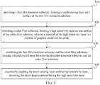
- a method of manufacturing the touch display device having a high resistivity layer includes the following steps: In step S10, a thin film transistor substrate is provided, and a touch sensing layer is formed on a surface of the thin film transistor substrate.
- the touch sensing layer 40 is made of ITO.
- the material of the touch sensing layer 40 is not limited to ITO, but may be other conductive materials such as AZO.
- the surface of the thin film transistor substrate can be coated by a screen printing method or a vacuum magnetron sputtering method, and pattern fabrication can be performed by a chemical etching method, thereby obtaining the touch sensing layer.
- the touch sensing layer is formed on the surface of the thin film transistor substrate facing the color filter substrate.
- step S20 a color filter substrate is provided, and a high resistivity layer is formed on one surface of the color filter substrate.
- a material of the high resistivity layer is a mixture of graphite oxide and tin oxide.
- a target material can be sputtered onto the surface of the color filter substrate away from the thin film transistor substrate by means of vacuum magnetron sputtering to form the high resistivity layer.
- the target material is a mixture of graphite oxide and tin oxide.
- the target material is a mixture of graphite oxide and tin oxide with a mass ratio of 60:100 to 70:100.
- the target material is a mixture of graphite oxide and tin oxide with a mass ratio of 40.4:59.6.
- the specific process conditions of the vacuum magnetron sputtering are: a coating chamber has a vacuum degree of 2.5 ⁇ 10 -1 Pa to 3.5 ⁇ 10 -2 Pa, the color filter substrate has a surface temperature of 80 °C to 100 °C, the color filter substrate is heated for 1390 s to 1410 s, a mixed gas has a flow rate of 1265 sccm to 1419 sccm, a voltage is 380 V to 480 V, an anaerobic voltage is 680 V to 760 V, a peroxy voltage is 300 V to 330 V, a power is 6300 W to 7500 W, and a target sputtering distance is 40 mm.
- the amount of oxygen can be determined by voltage, anaerobic voltage, and peroxy voltage. If the voltage is too high, the target material may be poisoned.
- the mixed gas is a mixture of oxygen and argon, wherein the oxygen has a flow rate of 35 sccm to 39 sccm, the argon has a flow rate of 1230 sccm to 1380 sccm.
- the purities of oxygen and argon are greater than or equal to 99.999%.
- the effect of argon is that: under the action of the electrons and vacuum degree of the coating chamber, the argon becomes argon ions.
- the sputtered atoms are deposited on a surface of the substrate to form a thin film.
- the effect of oxygen is that: the oxygen oxidizes the surface of the target and particles that have been sputtered, such that a high resistivity layer with a good transmission of light is formed by vacuum magnetron sputtering.
- the color filter substrate is heated to a temperature of 100 °C by using intermediate frequency vacuum magnetron sputtering, a surface temperature difference of the color filter substrate is less than or equal to 1.5 °C, and the color filter substrate is heated for 1400 s.
- the coating chamber has a vacuum degree of 2.5 ⁇ 10 -1 Pa to 3.5 ⁇ 10 -2 Pa.
- An operating speed of the substrate in the coating chamber is 1.0 m/min to 1.5 m/min, and the coating time is 120 s.
- the oxygen has a flow rate of 35 sccm to 39sccm
- the argon has a flow rate of 1230 sccm to 1380sccm
- a voltage is 465 V
- an anaerobic voltage is 725 V
- a peroxy voltage is 313 V
- a sputtering power is 6300 W to 7500 W
- a target sputtering distance is 40 mm.
- the color filter substrate may be subjected to a cleaning treatment, a drying treatment, and an electrostatic dissipation treatment in sequence.
- An operation of the cleaning treatment includes performing a pure water cleaning, a lye cleaning, a two-fluid spray cleaning, a ultra-pure water spray cleaning, and a high pressure spray cleaning in sequence.
- the lye can be a cleaning agent, such as a glass cleaning agent containing potassium hydroxide or sodium hydroxide.
- the two-fluid spray means that droplets formed by the high pressure gas and the cleaning fluid are sprayed at high speed through the nozzle to clean the surface of the object, after the high pressure gaseous fluid such as air is mixed with the liquid fluid such as water.
- the pure water in the ultra-pure water spray refers to water which resistivity is greater than or equal to 8 M ⁇ .
- the drying treatment includes performing a cold air drying and a hot air drying in sequence. It should be noted that, if the color filter substrate itself is clean without dirt and dust, this step can be omitted.
- step S30 the thin film transistor substrate and the color filter substrate are combined to form a liquid crystal layer, which is located between the thin film transistor substrate and the color filter substrate.
- the high resistivity layer is located on the surface of the color filter substrate away from the thin film transistor substrate, and the touch sensing layer is sandwiched between the thin film transistor substrate and the liquid crystal layer.
- the touch sensing layer is located on the surface of the thin film transistor substrate away from the liquid crystal layer.
- the liquid crystal layer can be made of organic matters such as aliphatic, aromatic, stearic acid.
- the liquid crystal layer can be formed between the thin film transistor substrate and the color filter substrate by a liquid crystal perfusion method. In other words, after the thin film transistor substrate and the color filter substrate are aligned and assembled, the liquid crystal is sucked to form the liquid crystal layer by the capillary principle. Alternatively, using a liquid crystal injection method, the liquid crystal is directly dropped onto the color filter substrate, and then the thin film transistor substrate and the color filter substrate are aligned and assembled.
- step S40 the touch sensing layer is electrically coupled to the high resistivity layer, thereby obtaining the touch display device having the high resistivity layer.
- the touch sensing layer can be electrically coupled to the high resistivity layer via a lead.
- the touch sensing layer is electrically coupled to the high resistivity layer to form a touch module.
- the thin film transistor substrate, the liquid crystal layer, and the color filter substrate form a display module.
- the touch module and the display module cooperatively form the touch display device having the high resistivity layer.
- an electrical coupling between the touch sensing layer and the high resistivity layer is not necessarily a direct contact between the touch sensing layer and the high resistivity layer, or may also be a coupling between the touch sensing layer and the high resistivity layer via electrode of the ITO terminal when the screen is manufactured.
- the steps of the aforementioned method of manufacturing the touch display device having the high resistivity layer are not limited to the aforementioned sequence, and may be adjusted as necessary.
- the touch display device having the high resistivity layer by forming the touch sensing layer on the surface of the thin film transistor substrate and forming the high resistivity layer on the surface of the color filter substrate away from the thin film transistor substrate, the high resistivity layer is electrically coupled to the touch sensing layer to form the touch module.
- the material of the high resistivity layer is the mixture of graphite oxide and tin oxide, which has excellent adsorption properties, such that an optical adhesive may not be required, and the process steps are relatively simple.
- the touch display device having the high resistivity layer manufactured by the aforementioned method has a thinner thickness, a better light transmittance, and an anti-static effect, such that the touch sensitivity is high.
- Instrument vacuum magnetron sputtering coating machine, cleaning machine, high resistance instrument, film thickness gauge, spectrometer, colorimeter, and so on.
- the high resistivity layer was formed on the surface of the color filter substrate, which includes the following steps of:
- a thickness of the high resistivity layer was measured by the film thickness gauge, which was 18 nm.
- a transmittance of the high resistivity layer was measured by the spectrometer, which was 96.8%.
- the manufacturing of the touch display device having the high resistivity layer also includes the manufacturing of a cover plate, a polarizer, and a lead, a conventional method may be employed, and is not limited thereto.
- a resistance of the high resistivity layer was measured by a resistance instrument, which was 5 ⁇ 10 8 ⁇ /cm 2 .
- a change rate of the resistance of the high resistivity layer was 22% when a baking experiment was carried out at 90 °C and 60% humidity for 240 hours in a temperature humidity chamber.
- the change rate of the resistance of the high resistivity layer was 24% after 5 minutes of alcohol immersion.
- the change rate of the resistance was 7% when baked at 60 °C in an oven with pad for 240 hours.
- the high resistivity layer was formed on the surface of the color filter substrate, which includes the following steps of:
- a thickness of the high resistivity layer was measured by the film thickness gauge, which was 18 nm.
- a transmittance of the high resistivity layer was measured by the spectrometer, which was 97%.
- the manufacturing of the touch display device having the high resistivity layer also includes the manufacturing of a cover plate, a polarizer, and a lead, a conventional method may be employed, and is not limited thereto.
- a resistance of the high resistivity layer was measured by a resistance instrument, which was 5 ⁇ 10 8 ⁇ /cm 2 .
- a change rate of the resistance of the high resistivity layer was 21% when a baking experiment was carried out at 90 °C and 60% humidity for 240 hours in a temperature humidity chamber.
- the change rate of the resistance of the high resistivity layer was 24% after 5 minutes of alcohol immersion.
- the change rate of the resistance was 8% when baked at 60 °C in an oven with pad for 240 hours.
- the high resistivity layer was formed on the surface of the color filter substrate, which includes the following steps of:
- a thickness of the high resistivity layer was measured by the film thickness gauge, which was 18 nm.
- a transmittance of the high resistivity layer was measured by the spectrometer, which was 96.5%.
- the manufacturing of the touch display device having the high resistivity layer also includes the manufacturing of a cover plate, a polarizer, and a lead, a conventional method may be employed, and is not limited thereto.
- a resistance of the high resistivity layer was measured by a resistance instrument, which was 5 ⁇ 10 8 ⁇ /cm 2 .
- a change rate of the resistance of the high resistivity layer was 19% when a baking experiment was carried out at 90 °C and 60% humidity for 240 hours in a temperature humidity chamber.
- the change rate of the resistance of the high resistivity layer was 22% after 5 minutes of alcohol immersion.
- the change rate of the resistance was 9% when baked at 60 °C in an oven with pad for 240 hours.
Landscapes
- Physics & Mathematics (AREA)
- Engineering & Computer Science (AREA)
- Theoretical Computer Science (AREA)
- General Engineering & Computer Science (AREA)
- General Physics & Mathematics (AREA)
- Nonlinear Science (AREA)
- Human Computer Interaction (AREA)
- Electromagnetism (AREA)
- Optics & Photonics (AREA)
- Crystallography & Structural Chemistry (AREA)
- Chemical & Material Sciences (AREA)
- Mathematical Physics (AREA)
- Liquid Crystal (AREA)
- Physical Vapour Deposition (AREA)
- Microelectronics & Electronic Packaging (AREA)
- Devices For Indicating Variable Information By Combining Individual Elements (AREA)
Claims (13)
- Touch-Display-Vorrichtung (100) mit: einem Dünnfilm-Transistorsubstrat (10), einer Berührungssensierschicht (40), einer Flüssigkristallschicht (20), einem Farbfiltersubstrat (30) und einer Hochwiderstandsschicht (50), die der Reihe nach geschichtet sind; wobei ein Material der Hochwiderstandsschicht (50) eine Mischung aus Graphitoxid und Zinnoxid ist,
dadurch gekennzeichnet, dass
das Material der Hochwiderstandsschicht (50) eine Mischung aus Graphitoxid und Zinnoxid ist mit einem Massenverhältnis von 60:100 bis 70:100. - Touch-Display-Vorrichtung nach Anspruch 1, wobei das Material der Hochwiderstandsschicht (50) eine Mischung aus Graphitoxid und Zinnoxid ist mit einem Massenverhältnis von 40,4:59,6.
- Touch-Display-Vorrichtung nach Anspruch 1, wobei die Berührungssensierschicht (40) und die Hochwiderstandsschicht (50) über einen Anschlussdraht elektrisch gekoppelt sind.
- Touch-Display-Vorrichtung nach Anspruch 1, wobei die Hochwiderstandsschicht (50) eine Dicke von 12 nm bis 25 nm aufweist.
- Touch-Display-Vorrichtung nach Anspruch 1, wobei eine Lichtdurchlässigkeit der Hochwiderstandsschicht (50) größer als oder gleich 96 % ist, wobei sich die vorliegend verwendete Lichtdurchlässigkeit auf eine Lichtdurchlässigkeit des Farbfiltersubstrats nach dem Bilden der Hochwiderstandsschicht auf einer Oberfläche des Farbfiltersubstrats und auf eine Lichtdurchlässigkeit des Farbfiltersubstrats vor dem Bilden der Hochwiderstandsschicht auf dem Farbfiltersubtrat bezieht.
- Touch-Display-Vorrichtung nach Anspruch 1, wobei die Berührungssensierschicht (40) aus Indiumzinnoxid (ITO) besteht.
- Touch-Display-Vorrichtung (100) mit: einer Berührungssensierschicht (40), einem Dünnfilm-Transistorsubstrat (10), einer Flüssigkristallschicht (20), einem Farbfiltersubstrat (30) und einer Hochwiderstandsschicht (50), die der Reihe nach geschichtet sind; wobei ein Material der Hochwiderstandsschicht (50) eine Mischung aus Graphitoxid und Zinnoxid ist,
dadurch gekennzeichnet, dass
das Material der Hochwiderstandsschicht (50) eine Mischung aus Graphitoxid und Zinnoxid ist mit einem Massenverhältnis von 60:100 bis 70:100. - Verfahren zur Herstellung einer Touch-Display-Vorrichtung mit folgenden Schritten:Bereitstellen (S10) eines Dünnfilm-Transistorsubstrats, Bilden einer Berührungssensierschicht auf einer Oberfläche des Dünnfilm-Transistorsubstrats;Bereitstellen (S20) eines Farbfiltersubstrats, Bilden einer Hochwiderstandsschicht auf einer Oberfläche des Farbfiltersubstrats, wobei ein Material der Hochwiderstandsschicht eine Mischung aus Graphitoxid und Zinnoxid ist;Kombinieren (S30) des Dünnfilm-Transistorsubstrats und des Farbfiltersubstrats, Bilden einer Flüssigkristallschicht zwischen dem Dünnfilm-Transistorsubstrat und dem Farbfiltersubstrat, wobei sich die Hochwiderstandsschicht auf einer Oberfläche des Farbfiltersubstrats entfernt von dem Dünnfilm-Transistorsubstrat befindet, wobei die Berührungssensierschicht sandwichartig zwischen dem Dünnfilm-Transistorsubstrat und der Flüssigkristallschicht angeordnet ist; undelektrisches Koppeln (S40) der Berührungssensierschicht und der Hochwiderstandsschicht, wodurch die Touch-Display-Vorrichtung mit der Hochwiderstandsschicht erhalten wird,dadurch gekennzeichnet, dassdas Material der Hochwiderstandsschicht eine Mischung aus Graphitoxid und Zinnoxid ist mit einem Massenverhältnis von 60:100 bis 70:100.
- Verfahren nach Anspruch 8, wobei der Vorgang des Bildens der Hochwiderstandsschicht auf einer Oberfläche des Farbfiltersubstrats umfasst:
Sputtern der Mischung aus Graphitoxid und Zinnoxid auf eine Oberfläche des Farbfiltersubstrats durch Vakuum-Magnetron-Sputtern, wobei eine Beschichtungskammer einen Vakuumgrad von 2,5 x 10⁻¹ Pa bis 3,5 x 10⁻² Pa aufweist, das Farbfiltersubstrat eine Oberflächentemperatur von 80 °C aufweist, das Farbfiltersubstrat 1390 bis 1410 Sekunden lang erwärmt wird, ein Mischgas eine Strömungsrate von 1265 sccm bis 1419 sccm aufweist, eine Spannung 380 V bis 480 V beträgt, eine anaerobe Spannung 680 V bis 760 V beträgt, eine Peroxy-Spannung 300 V bis 330 V beträgt, eine Leistung 6300 W bis 7500 W beträgt und ein Soll-Sputterabstand 40 mm beträgt. - Verfahren nach Anspruch 9, wobei das Mischgas eine Mischung aus Sauerstoff und Argon ist, wobei der Sauerstoff eine Strömungsrate von 35 sccm bit 39 sccm aufweist und das Argon eine Strömungsrate von 1230 sccm bis 1380 sccm aufweist.
- Verfahren nach Anspruch 9, wobei die Mischung aus Graphitoxid und Zinnoxid ein Massenverhältnis von 40,4:59,6 aufweist.
- Verfahren nach Anspruch 8, wobei vor dem Vorgang des Bildens der Hochwiderstandsschicht auf einer Oberfläche des Farbfiltersubstrats, das Verfahren ferner umfasst:
Durchführen einer Reinigungsbehandlung, einer Trocknungsbehandlung und einer elektrostatischen Dissipationsbehandlung der Reihe nach mit dem Farbfiltersubstrat; wobei ein Vorgang der Reinigungsbehandlung das Durchführen einer Reinwasserreinigung, einer Laugenreinigung, einer Zwei-Fluid-Sprühreinigung, einer Reinstwasser-Sprühreinigung und einer Hochdruck-Sprühreinigung der Reihe nach umfasst; wobei die Trocknungsbehandlung das Durchführen einer Kaltluftrocknung und einer Heißlufttrocknung der Reihe nach umfasst. - Verfahren nach Anspruch 8, wobei die Berührungssensierschicht und die Hochwiderstandschicht über einen Anschlussdraht elektrisch gekoppelt sind.
Applications Claiming Priority (2)
| Application Number | Priority Date | Filing Date | Title |
|---|---|---|---|
| CN201510688739.0A CN105242809A (zh) | 2015-10-21 | 2015-10-21 | 触控显示装置及其制备方法 |
| PCT/CN2016/102792 WO2017067492A1 (zh) | 2015-10-21 | 2016-10-21 | 具有高阻层的触控显示装置及其制备方法 |
Publications (3)
| Publication Number | Publication Date |
|---|---|
| EP3285152A1 EP3285152A1 (de) | 2018-02-21 |
| EP3285152A4 EP3285152A4 (de) | 2018-12-26 |
| EP3285152B1 true EP3285152B1 (de) | 2020-03-04 |
Family
ID=55040477
Family Applications (1)
| Application Number | Title | Priority Date | Filing Date |
|---|---|---|---|
| EP16856923.4A Active EP3285152B1 (de) | 2015-10-21 | 2016-10-21 | Berührungssteuerungsanzeigevorrichtung mit hochresistenter schicht |
Country Status (7)
| Country | Link |
|---|---|
| US (1) | US10365508B2 (de) |
| EP (1) | EP3285152B1 (de) |
| JP (1) | JP6526913B2 (de) |
| CN (1) | CN105242809A (de) |
| DK (1) | DK3285152T3 (de) |
| ES (1) | ES2791478T3 (de) |
| WO (1) | WO2017067492A1 (de) |
Families Citing this family (6)
| Publication number | Priority date | Publication date | Assignee | Title |
|---|---|---|---|---|
| CN105242809A (zh) * | 2015-10-21 | 2016-01-13 | 江西沃格光电股份有限公司 | 触控显示装置及其制备方法 |
| CN106756843A (zh) * | 2016-12-20 | 2017-05-31 | 赫得纳米科技(昆山)有限公司 | 一种防静电干扰层的制备方法 |
| CN110828530A (zh) * | 2019-11-28 | 2020-02-21 | 武汉华星光电半导体显示技术有限公司 | 一种显示面板及其制备方法、显示装置 |
| CN113337796B (zh) * | 2020-03-02 | 2022-06-28 | 北京大学 | 一种光截止性滤光片及其制备方法和应用 |
| CN112111715A (zh) * | 2020-09-22 | 2020-12-22 | 长沙壹纳光电材料有限公司 | 一种改善高阻膜方阻稳定性的方法及系统 |
| CN112853268A (zh) * | 2021-02-07 | 2021-05-28 | 天津盛诺电子科技有限公司 | 一种车载显示屏镀膜工艺 |
Family Cites Families (19)
| Publication number | Priority date | Publication date | Assignee | Title |
|---|---|---|---|---|
| DE4214729C1 (de) | 1992-05-08 | 1993-09-16 | Sundwiger Eisenhuette Maschinenfabrik Gmbh & Co, 58675 Hemer, De | |
| JP2859790B2 (ja) | 1993-02-10 | 1999-02-24 | 住友大阪セメント株式会社 | 帯電防止・高屈折率膜形成用塗料および帯電防止・反射防止膜付き透明材料積層体および表示装置 |
| US6896981B2 (en) * | 2001-07-24 | 2005-05-24 | Bridgestone Corporation | Transparent conductive film and touch panel |
| JP2009117597A (ja) | 2007-11-06 | 2009-05-28 | Dainippon Screen Mfg Co Ltd | 基板処理装置および基板処理方法 |
| US8692948B2 (en) * | 2010-05-21 | 2014-04-08 | Apple Inc. | Electric field shielding for in-cell touch type thin-film-transistor liquid crystal displays |
| JP5977260B2 (ja) * | 2011-02-02 | 2016-08-24 | スリーエム イノベイティブ プロパティズ カンパニー | 暗い多層導電体トレースを有するパターン化基材 |
| JP2012247542A (ja) | 2011-05-26 | 2012-12-13 | Japan Display Central Co Ltd | 液晶表示装置 |
| WO2013158641A2 (en) | 2012-04-16 | 2013-10-24 | Vorbeck Materials | Capacitive touch device brush stylus |
| US9001280B2 (en) * | 2012-06-08 | 2015-04-07 | Apple Inc. | Devices and methods for shielding displays from electrostatic discharge |
| CN102955613A (zh) * | 2012-10-26 | 2013-03-06 | 北京京东方光电科技有限公司 | 一种触控显示屏及触控显示装置 |
| CN102999223A (zh) * | 2012-12-25 | 2013-03-27 | 北京京东方光电科技有限公司 | 一种触控显示屏及触控显示装置 |
| JP2014177552A (ja) | 2013-03-14 | 2014-09-25 | Hitachi Maxell Ltd | 透明導電性コーティング組成物、透明導電性膜及びタッチパネル機能内蔵型横電界方式液晶表示パネル |
| JP6101123B2 (ja) * | 2013-03-18 | 2017-03-22 | アルプス電気株式会社 | 静電容量式タッチパッド |
| TW201441883A (zh) * | 2013-04-29 | 2014-11-01 | Ye Xin Technology Consulting Co Ltd | 內嵌式觸控顯示裝置 |
| KR102568895B1 (ko) * | 2014-03-13 | 2023-08-21 | 가부시키가이샤 한도오따이 에네루기 켄큐쇼 | 전자 장치 |
| CN104571714B (zh) * | 2015-01-30 | 2018-11-23 | 京东方科技集团股份有限公司 | 触摸屏和显示装置 |
| CN105242431B (zh) * | 2015-10-21 | 2018-11-09 | 江西沃格光电股份有限公司 | 具有消除静电的高阻层的触控显示装置及其制备方法 |
| CN105242432A (zh) * | 2015-10-21 | 2016-01-13 | 江西沃格光电股份有限公司 | 触控显示装置及其制备方法 |
| CN105242809A (zh) * | 2015-10-21 | 2016-01-13 | 江西沃格光电股份有限公司 | 触控显示装置及其制备方法 |
-
2015
- 2015-10-21 CN CN201510688739.0A patent/CN105242809A/zh active Pending
-
2016
- 2016-10-21 WO PCT/CN2016/102792 patent/WO2017067492A1/zh not_active Ceased
- 2016-10-21 DK DK16856923.4T patent/DK3285152T3/da active
- 2016-10-21 EP EP16856923.4A patent/EP3285152B1/de active Active
- 2016-10-21 JP JP2018513716A patent/JP6526913B2/ja active Active
- 2016-10-21 US US15/735,603 patent/US10365508B2/en active Active
- 2016-10-21 ES ES16856923T patent/ES2791478T3/es active Active
Non-Patent Citations (1)
| Title |
|---|
| None * |
Also Published As
| Publication number | Publication date |
|---|---|
| JP6526913B2 (ja) | 2019-06-05 |
| US10365508B2 (en) | 2019-07-30 |
| ES2791478T3 (es) | 2020-11-04 |
| WO2017067492A1 (zh) | 2017-04-27 |
| CN105242809A (zh) | 2016-01-13 |
| JP2018518787A (ja) | 2018-07-12 |
| EP3285152A1 (de) | 2018-02-21 |
| EP3285152A4 (de) | 2018-12-26 |
| US20180314094A1 (en) | 2018-11-01 |
| DK3285152T3 (da) | 2020-05-18 |
Similar Documents
| Publication | Publication Date | Title |
|---|---|---|
| EP3285152B1 (de) | Berührungssteuerungsanzeigevorrichtung mit hochresistenter schicht | |
| US20140020810A1 (en) | Capacitive touch panel, manufacturing method therefor and liquid crystal display apparatus provided with the touch panel | |
| TWI552169B (zh) | A transparent conductive film, a substrate having a transparent conductive film, a IPS liquid crystal cell, an electrostatic capacitive touch panel, and a substrate having a transparent conductive film | |
| US20100065342A1 (en) | Touch screen having reduced reflection | |
| CN103218102B (zh) | 一种电容屏用双面镀膜玻璃的加工方法及双面镀膜玻璃 | |
| CN104090677A (zh) | 一种内嵌式触摸屏和显示装置 | |
| CN106662950A (zh) | 导电结构及其制造方法 | |
| JP6495541B2 (ja) | 高抵抗率膜を有する埋設タッチパネル及びディスプレイデバイス | |
| CN104461157B (zh) | 触摸面板的制作方法、触摸面板、触摸屏和显示装置 | |
| TWI564760B (zh) | 觸控面板及其製造方法 | |
| CN105242431B (zh) | 具有消除静电的高阻层的触控显示装置及其制备方法 | |
| CN108028094A (zh) | 带透明导电层的基板、液晶面板、以及带透明导电层的基板的制造方法 | |
| CN107197627A (zh) | 导电结构体及其制造方法 | |
| CN105819703A (zh) | 一种具有消影功能的电容式触摸屏用导电玻璃的制备方法 | |
| CN105242432A (zh) | 触控显示装置及其制备方法 | |
| CN107430466B (zh) | 用于触摸屏面板的层状系统、用于触摸屏面板的层状系统的制造方法及触摸屏面板 | |
| US20190064569A1 (en) | Antistatic film and display input device | |
| KR101171663B1 (ko) | 시인성 향상과 인쇄층을 겸비한 터치패널 | |
| KR101385972B1 (ko) | 시인성 향상과 인쇄층을 겸비한 터치패널 | |
| KR101248783B1 (ko) | 시인성과 슬림화를 겸비한 터치패널 | |
| KR101216999B1 (ko) | 시인성 향상과 슬림화를 겸비한 터치패널 | |
| KR101163706B1 (ko) | 시인성 향상과 인쇄층을 겸비한 터치패널 | |
| JP2013175240A (ja) | 静電容量式タッチパネル及び該タッチパネルを備えた液晶表示装置 | |
| KR20120087800A (ko) | 시인성 향상과 인쇄층을 겸비한 터치패널 |
Legal Events
| Date | Code | Title | Description |
|---|---|---|---|
| STAA | Information on the status of an ep patent application or granted ep patent |
Free format text: STATUS: THE INTERNATIONAL PUBLICATION HAS BEEN MADE |
|
| PUAI | Public reference made under article 153(3) epc to a published international application that has entered the european phase |
Free format text: ORIGINAL CODE: 0009012 |
|
| STAA | Information on the status of an ep patent application or granted ep patent |
Free format text: STATUS: REQUEST FOR EXAMINATION WAS MADE |
|
| 17P | Request for examination filed |
Effective date: 20171117 |
|
| AK | Designated contracting states |
Kind code of ref document: A1 Designated state(s): AL AT BE BG CH CY CZ DE DK EE ES FI FR GB GR HR HU IE IS IT LI LT LU LV MC MK MT NL NO PL PT RO RS SE SI SK SM TR |
|
| AX | Request for extension of the european patent |
Extension state: BA ME |
|
| A4 | Supplementary search report drawn up and despatched |
Effective date: 20181128 |
|
| RIC1 | Information provided on ipc code assigned before grant |
Ipc: H01L 51/44 20060101ALI20181123BHEP Ipc: H01L 29/16 20060101ALI20181123BHEP Ipc: G02F 1/1335 20060101ALI20181123BHEP Ipc: G06F 3/041 20060101AFI20181123BHEP Ipc: G02F 1/1368 20060101ALI20181123BHEP Ipc: G02F 1/1333 20060101ALI20181123BHEP |
|
| DAV | Request for validation of the european patent (deleted) | ||
| DAX | Request for extension of the european patent (deleted) | ||
| GRAP | Despatch of communication of intention to grant a patent |
Free format text: ORIGINAL CODE: EPIDOSNIGR1 |
|
| STAA | Information on the status of an ep patent application or granted ep patent |
Free format text: STATUS: GRANT OF PATENT IS INTENDED |
|
| RIC1 | Information provided on ipc code assigned before grant |
Ipc: H01L 29/16 20060101ALI20190816BHEP Ipc: G02F 1/1335 20060101ALI20190816BHEP Ipc: G02F 1/1368 20060101ALI20190816BHEP Ipc: G06F 3/041 20060101AFI20190816BHEP Ipc: H01L 51/44 20060101ALI20190816BHEP Ipc: G02F 1/1333 20060101ALI20190816BHEP |
|
| INTG | Intention to grant announced |
Effective date: 20190916 |
|
| RIN1 | Information on inventor provided before grant (corrected) |
Inventor name: KUANG, JUNWEN Inventor name: ZHOU, HUIRONG Inventor name: YI, WEIHUA Inventor name: ZHANG, XUN Inventor name: ZHANG, BOLUN |
|
| GRAS | Grant fee paid |
Free format text: ORIGINAL CODE: EPIDOSNIGR3 |
|
| GRAA | (expected) grant |
Free format text: ORIGINAL CODE: 0009210 |
|
| STAA | Information on the status of an ep patent application or granted ep patent |
Free format text: STATUS: THE PATENT HAS BEEN GRANTED |
|
| AK | Designated contracting states |
Kind code of ref document: B1 Designated state(s): AL AT BE BG CH CY CZ DE DK EE ES FI FR GB GR HR HU IE IS IT LI LT LU LV MC MK MT NL NO PL PT RO RS SE SI SK SM TR |
|
| REG | Reference to a national code |
Ref country code: GB Ref legal event code: FG4D |
|
| REG | Reference to a national code |
Ref country code: CH Ref legal event code: EP |
|
| REG | Reference to a national code |
Ref country code: AT Ref legal event code: REF Ref document number: 1241149 Country of ref document: AT Kind code of ref document: T Effective date: 20200315 |
|
| REG | Reference to a national code |
Ref country code: DE Ref legal event code: R096 Ref document number: 602016031282 Country of ref document: DE |
|
| REG | Reference to a national code |
Ref country code: IE Ref legal event code: FG4D |
|
| REG | Reference to a national code |
Ref country code: FI Ref legal event code: FGE |
|
| REG | Reference to a national code |
Ref country code: DK Ref legal event code: T3 Effective date: 20200512 |
|
| REG | Reference to a national code |
Ref country code: SE Ref legal event code: TRGR |
|
| REG | Reference to a national code |
Ref country code: GR Ref legal event code: EP Ref document number: 20200401402 Country of ref document: GR Effective date: 20200716 |
|
| PG25 | Lapsed in a contracting state [announced via postgrant information from national office to epo] |
Ref country code: NO Free format text: LAPSE BECAUSE OF FAILURE TO SUBMIT A TRANSLATION OF THE DESCRIPTION OR TO PAY THE FEE WITHIN THE PRESCRIBED TIME-LIMIT Effective date: 20200604 Ref country code: RS Free format text: LAPSE BECAUSE OF FAILURE TO SUBMIT A TRANSLATION OF THE DESCRIPTION OR TO PAY THE FEE WITHIN THE PRESCRIBED TIME-LIMIT Effective date: 20200304 |
|
| REG | Reference to a national code |
Ref country code: NL Ref legal event code: MP Effective date: 20200304 |
|
| PG25 | Lapsed in a contracting state [announced via postgrant information from national office to epo] |
Ref country code: BG Free format text: LAPSE BECAUSE OF FAILURE TO SUBMIT A TRANSLATION OF THE DESCRIPTION OR TO PAY THE FEE WITHIN THE PRESCRIBED TIME-LIMIT Effective date: 20200604 Ref country code: HR Free format text: LAPSE BECAUSE OF FAILURE TO SUBMIT A TRANSLATION OF THE DESCRIPTION OR TO PAY THE FEE WITHIN THE PRESCRIBED TIME-LIMIT Effective date: 20200304 Ref country code: LV Free format text: LAPSE BECAUSE OF FAILURE TO SUBMIT A TRANSLATION OF THE DESCRIPTION OR TO PAY THE FEE WITHIN THE PRESCRIBED TIME-LIMIT Effective date: 20200304 |
|
| REG | Reference to a national code |
Ref country code: LT Ref legal event code: MG4D |
|
| PG25 | Lapsed in a contracting state [announced via postgrant information from national office to epo] |
Ref country code: NL Free format text: LAPSE BECAUSE OF FAILURE TO SUBMIT A TRANSLATION OF THE DESCRIPTION OR TO PAY THE FEE WITHIN THE PRESCRIBED TIME-LIMIT Effective date: 20200304 |
|
| PG25 | Lapsed in a contracting state [announced via postgrant information from national office to epo] |
Ref country code: PT Free format text: LAPSE BECAUSE OF FAILURE TO SUBMIT A TRANSLATION OF THE DESCRIPTION OR TO PAY THE FEE WITHIN THE PRESCRIBED TIME-LIMIT Effective date: 20200729 Ref country code: CZ Free format text: LAPSE BECAUSE OF FAILURE TO SUBMIT A TRANSLATION OF THE DESCRIPTION OR TO PAY THE FEE WITHIN THE PRESCRIBED TIME-LIMIT Effective date: 20200304 Ref country code: RO Free format text: LAPSE BECAUSE OF FAILURE TO SUBMIT A TRANSLATION OF THE DESCRIPTION OR TO PAY THE FEE WITHIN THE PRESCRIBED TIME-LIMIT Effective date: 20200304 Ref country code: LT Free format text: LAPSE BECAUSE OF FAILURE TO SUBMIT A TRANSLATION OF THE DESCRIPTION OR TO PAY THE FEE WITHIN THE PRESCRIBED TIME-LIMIT Effective date: 20200304 Ref country code: SM Free format text: LAPSE BECAUSE OF FAILURE TO SUBMIT A TRANSLATION OF THE DESCRIPTION OR TO PAY THE FEE WITHIN THE PRESCRIBED TIME-LIMIT Effective date: 20200304 Ref country code: EE Free format text: LAPSE BECAUSE OF FAILURE TO SUBMIT A TRANSLATION OF THE DESCRIPTION OR TO PAY THE FEE WITHIN THE PRESCRIBED TIME-LIMIT Effective date: 20200304 Ref country code: SK Free format text: LAPSE BECAUSE OF FAILURE TO SUBMIT A TRANSLATION OF THE DESCRIPTION OR TO PAY THE FEE WITHIN THE PRESCRIBED TIME-LIMIT Effective date: 20200304 Ref country code: IS Free format text: LAPSE BECAUSE OF FAILURE TO SUBMIT A TRANSLATION OF THE DESCRIPTION OR TO PAY THE FEE WITHIN THE PRESCRIBED TIME-LIMIT Effective date: 20200704 |
|
| REG | Reference to a national code |
Ref country code: ES Ref legal event code: FG2A Ref document number: 2791478 Country of ref document: ES Kind code of ref document: T3 Effective date: 20201104 |
|
| REG | Reference to a national code |
Ref country code: AT Ref legal event code: MK05 Ref document number: 1241149 Country of ref document: AT Kind code of ref document: T Effective date: 20200304 |
|
| REG | Reference to a national code |
Ref country code: DE Ref legal event code: R097 Ref document number: 602016031282 Country of ref document: DE |
|
| PLBE | No opposition filed within time limit |
Free format text: ORIGINAL CODE: 0009261 |
|
| STAA | Information on the status of an ep patent application or granted ep patent |
Free format text: STATUS: NO OPPOSITION FILED WITHIN TIME LIMIT |
|
| PG25 | Lapsed in a contracting state [announced via postgrant information from national office to epo] |
Ref country code: AT Free format text: LAPSE BECAUSE OF FAILURE TO SUBMIT A TRANSLATION OF THE DESCRIPTION OR TO PAY THE FEE WITHIN THE PRESCRIBED TIME-LIMIT Effective date: 20200304 Ref country code: IT Free format text: LAPSE BECAUSE OF FAILURE TO SUBMIT A TRANSLATION OF THE DESCRIPTION OR TO PAY THE FEE WITHIN THE PRESCRIBED TIME-LIMIT Effective date: 20200304 |
|
| 26N | No opposition filed |
Effective date: 20201207 |
|
| PG25 | Lapsed in a contracting state [announced via postgrant information from national office to epo] |
Ref country code: SI Free format text: LAPSE BECAUSE OF FAILURE TO SUBMIT A TRANSLATION OF THE DESCRIPTION OR TO PAY THE FEE WITHIN THE PRESCRIBED TIME-LIMIT Effective date: 20200304 Ref country code: PL Free format text: LAPSE BECAUSE OF FAILURE TO SUBMIT A TRANSLATION OF THE DESCRIPTION OR TO PAY THE FEE WITHIN THE PRESCRIBED TIME-LIMIT Effective date: 20200304 |
|
| REG | Reference to a national code |
Ref country code: CH Ref legal event code: PL |
|
| PG25 | Lapsed in a contracting state [announced via postgrant information from national office to epo] |
Ref country code: MC Free format text: LAPSE BECAUSE OF FAILURE TO SUBMIT A TRANSLATION OF THE DESCRIPTION OR TO PAY THE FEE WITHIN THE PRESCRIBED TIME-LIMIT Effective date: 20200304 Ref country code: LU Free format text: LAPSE BECAUSE OF NON-PAYMENT OF DUE FEES Effective date: 20201021 |
|
| REG | Reference to a national code |
Ref country code: BE Ref legal event code: MM Effective date: 20201031 |
|
| PG25 | Lapsed in a contracting state [announced via postgrant information from national office to epo] |
Ref country code: CH Free format text: LAPSE BECAUSE OF NON-PAYMENT OF DUE FEES Effective date: 20201031 Ref country code: BE Free format text: LAPSE BECAUSE OF NON-PAYMENT OF DUE FEES Effective date: 20201031 Ref country code: LI Free format text: LAPSE BECAUSE OF NON-PAYMENT OF DUE FEES Effective date: 20201031 |
|
| PG25 | Lapsed in a contracting state [announced via postgrant information from national office to epo] |
Ref country code: IE Free format text: LAPSE BECAUSE OF NON-PAYMENT OF DUE FEES Effective date: 20201021 |
|
| PG25 | Lapsed in a contracting state [announced via postgrant information from national office to epo] |
Ref country code: MT Free format text: LAPSE BECAUSE OF FAILURE TO SUBMIT A TRANSLATION OF THE DESCRIPTION OR TO PAY THE FEE WITHIN THE PRESCRIBED TIME-LIMIT Effective date: 20200304 Ref country code: CY Free format text: LAPSE BECAUSE OF FAILURE TO SUBMIT A TRANSLATION OF THE DESCRIPTION OR TO PAY THE FEE WITHIN THE PRESCRIBED TIME-LIMIT Effective date: 20200304 |
|
| PG25 | Lapsed in a contracting state [announced via postgrant information from national office to epo] |
Ref country code: MK Free format text: LAPSE BECAUSE OF FAILURE TO SUBMIT A TRANSLATION OF THE DESCRIPTION OR TO PAY THE FEE WITHIN THE PRESCRIBED TIME-LIMIT Effective date: 20200304 Ref country code: AL Free format text: LAPSE BECAUSE OF FAILURE TO SUBMIT A TRANSLATION OF THE DESCRIPTION OR TO PAY THE FEE WITHIN THE PRESCRIBED TIME-LIMIT Effective date: 20200304 |
|
| P01 | Opt-out of the competence of the unified patent court (upc) registered |
Effective date: 20230530 |
|
| PGFP | Annual fee paid to national office [announced via postgrant information from national office to epo] |
Ref country code: DK Payment date: 20250924 Year of fee payment: 10 |
|
| PGFP | Annual fee paid to national office [announced via postgrant information from national office to epo] |
Ref country code: SE Payment date: 20250924 Year of fee payment: 10 |
|
| PGFP | Annual fee paid to national office [announced via postgrant information from national office to epo] |
Ref country code: DE Payment date: 20251020 Year of fee payment: 10 |
|
| PGFP | Annual fee paid to national office [announced via postgrant information from national office to epo] |
Ref country code: GB Payment date: 20251010 Year of fee payment: 10 |
|
| PGFP | Annual fee paid to national office [announced via postgrant information from national office to epo] |
Ref country code: FI Payment date: 20251028 Year of fee payment: 10 |
|
| PGFP | Annual fee paid to national office [announced via postgrant information from national office to epo] |
Ref country code: FR Payment date: 20251010 Year of fee payment: 10 |
|
| PGFP | Annual fee paid to national office [announced via postgrant information from national office to epo] |
Ref country code: GR Payment date: 20251022 Year of fee payment: 10 Ref country code: TR Payment date: 20251014 Year of fee payment: 10 |
|
| PGFP | Annual fee paid to national office [announced via postgrant information from national office to epo] |
Ref country code: ES Payment date: 20251114 Year of fee payment: 10 |