KR101171663B1 - 시인성 향상과 인쇄층을 겸비한 터치패널 - Google Patents
시인성 향상과 인쇄층을 겸비한 터치패널 Download PDFInfo
- Publication number
- KR101171663B1 KR101171663B1 KR1020110008822A KR20110008822A KR101171663B1 KR 101171663 B1 KR101171663 B1 KR 101171663B1 KR 1020110008822 A KR1020110008822 A KR 1020110008822A KR 20110008822 A KR20110008822 A KR 20110008822A KR 101171663 B1 KR101171663 B1 KR 101171663B1
- Authority
- KR
- South Korea
- Prior art keywords
- layer
- oxide layer
- indium tin
- tin oxide
- substrate
- Prior art date
- Legal status (The legal status is an assumption and is not a legal conclusion. Google has not performed a legal analysis and makes no representation as to the accuracy of the status listed.)
- Expired - Fee Related
Links
Images


Classifications
-
- G—PHYSICS
- G06—COMPUTING OR CALCULATING; COUNTING
- G06F—ELECTRIC DIGITAL DATA PROCESSING
- G06F3/00—Input arrangements for transferring data to be processed into a form capable of being handled by the computer; Output arrangements for transferring data from processing unit to output unit, e.g. interface arrangements
- G06F3/01—Input arrangements or combined input and output arrangements for interaction between user and computer
- G06F3/03—Arrangements for converting the position or the displacement of a member into a coded form
- G06F3/041—Digitisers, e.g. for touch screens or touch pads, characterised by the transducing means
- G06F3/0412—Digitisers structurally integrated in a display
-
- B—PERFORMING OPERATIONS; TRANSPORTING
- B32—LAYERED PRODUCTS
- B32B—LAYERED PRODUCTS, i.e. PRODUCTS BUILT-UP OF STRATA OF FLAT OR NON-FLAT, e.g. CELLULAR OR HONEYCOMB, FORM
- B32B33/00—Layered products characterised by particular properties or particular surface features, e.g. particular surface coatings; Layered products designed for particular purposes not covered by another single class
-
- B—PERFORMING OPERATIONS; TRANSPORTING
- B32—LAYERED PRODUCTS
- B32B—LAYERED PRODUCTS, i.e. PRODUCTS BUILT-UP OF STRATA OF FLAT OR NON-FLAT, e.g. CELLULAR OR HONEYCOMB, FORM
- B32B2457/00—Electrical equipment
- B32B2457/20—Displays, e.g. liquid crystal displays, plasma displays
- B32B2457/208—Touch screens
-
- G—PHYSICS
- G06—COMPUTING OR CALCULATING; COUNTING
- G06F—ELECTRIC DIGITAL DATA PROCESSING
- G06F2203/00—Indexing scheme relating to G06F3/00 - G06F3/048
- G06F2203/041—Indexing scheme relating to G06F3/041 - G06F3/045
- G06F2203/04103—Manufacturing, i.e. details related to manufacturing processes specially suited for touch sensitive devices
Landscapes
- Engineering & Computer Science (AREA)
- General Engineering & Computer Science (AREA)
- Theoretical Computer Science (AREA)
- Human Computer Interaction (AREA)
- Physics & Mathematics (AREA)
- General Physics & Mathematics (AREA)
- Position Input By Displaying (AREA)
Abstract
구성에 있어서, 글래스 ? PC(폴리카보네이트) ? PMMA(폴리메타메틸아크릴) 중에서 하나를 주재로 하는 기판(10); 및 상기 기판(10)의 일면에 인쇄층(21)과 산화니오븀층(22)을 증착하고; 산화니오븀층(22)의 상면에 다시 굴절율이 다른 물질을 다층으로 증착하여 형성되는 전도층(30);을 포함하여 이루어지는 것을 특징으로 한다.
이에 따라, 경량화/슬림화의 추세에 부응하면서 시인성을 향상하여 다양한 제품으로 응용이 가능하도록 하고, 더불어 인쇄층까지 일괄 형성하여 추가 제조공정의 번거로움까지 제거시킨 효과가 있다.
Description
도 2는 본 발명에 따른 터치패널의 주요구조 중 제2 산화인듐주석층이 제거된 상태의 상부 구성도
도 3(a)는 본 발명에 따른 제1 산화인듐주석층 상부에 PR노광처리 및 에칭액의 살포과정을 보여주는 상태도(a-a'선 단면 포함)
도 3(b)는 제1 산화인듐주석층 상면에 PR층이 제거되는 모습의 구성도
도 4(a)는 본 발명에 따른 절연막층 상부에 PR노광처리 과정을 보여주는 상태도
도 4(b)는 절연막층 상부의 에칭액 살포과정(도 4a의 b-b'선 단면 포함) 및 절연막층이 형성된 상태의 구성도
도 5(a)는 절연막층 상부에 제2 산화인듐주석층이 적층된 구성도
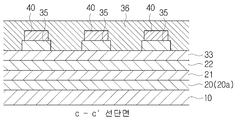
도 5(b)는 도 5a의 c-c'선 단면도이다.
20a: 하드코팅층 21: 인쇄층
22: 산화니오븀층 30: 전도층
33: 산화규소층 35: 제1 산화인듐주석층
36: 제2 산화인듐주석층 40: 절연막층
Claims (6)
- 터치패널에 있어서:
글래스, PC(폴리카보네이트), PMMA(폴리메타메틸아크릴) 중에서 하나를 주재로 하는 기판(10); 및
상기 기판(10)의 일면에 인쇄층(21)과 산화니오븀층(22)을 차례로 증착하고;
상기 산화니오븀층(22)의 상면에 굴절율이 다른 물질을 다층으로 증착하여 형성되는 전도층(30);을 포함하여 이루어지며,
상기 글래스 기판(10)은 소다라임 글래스 또는 고리라 글래스 중에서 선택되고, 기판(10)의 일면에 화학강화층(20)을 구비하되, 화학강화층(20)은 400~500℃ 내외의 질산칼륨용액에 2~8시간 내외로 침지하여 형성되는 것을 특징으로 하는 시인성 향상과 인쇄층을 겸비한 터치패널. - 삭제
- 제1항에 있어서,
상기 전도층(30)은 저굴절율을 지닌 산화규소층(33)과 고굴절율을 지닌 제1산화인듐주석층(35)을 증착하되, 상기 제1산화인듐주석층(35)의 양 가장자리를 제외한 상면부에 절연막층(40)을 형성하고, 제1산화인듐주석층(35) 및 절연막층(40) 상부의 전체 면에 제2산화인듐주석층(36)을 추가 형성하되, 제2산화인듐주석층(36)의 일측부는 절연막층(40)이 없는 제1산화인듐주석층(35)의 양 측 가장자리 부와 상호 연접되도록 함을 특징으로 하는 시인성 향상과 인쇄층을 겸비한 터치패널. - 제 1항에 있어서,
상기 PC 또는 PMMA의 기판(10)은 일면에 하드코팅층(20a)을 구비하고, 그 상면에 인쇄층(21)과 산화니오븀층(22) 및 전도층(30)을 차례로 증착하는 것을 특징으로 하는 시인성 향상과 인쇄층을 겸비한 터치패널. - 제1항 또는 제3항에 있어서,
상기 기판(10)은 상면에 산화인듐주석층(35)을 증착시킨 다음, 약 180~500℃내외의 진공챔버 내에 약 10~50분가량 재투입하여 저항치를 크게 낮출 수도 있음을 특징으로 하는 시인성 향상과 인쇄층을 겸비한 터치패널. - 삭제
Applications Claiming Priority (2)
| Application Number | Priority Date | Filing Date | Title |
|---|---|---|---|
| KR1020100138714 | 2010-12-29 | ||
| KR20100138714 | 2010-12-29 |
Related Child Applications (1)
| Application Number | Title | Priority Date | Filing Date |
|---|---|---|---|
| KR1020120000465A Division KR101385972B1 (ko) | 2012-01-03 | 2012-01-03 | 시인성 향상과 인쇄층을 겸비한 터치패널 |
Publications (2)
| Publication Number | Publication Date |
|---|---|
| KR20120076279A KR20120076279A (ko) | 2012-07-09 |
| KR101171663B1 true KR101171663B1 (ko) | 2012-08-07 |
Family
ID=46710016
Family Applications (1)
| Application Number | Title | Priority Date | Filing Date |
|---|---|---|---|
| KR1020110008822A Expired - Fee Related KR101171663B1 (ko) | 2010-12-29 | 2011-01-28 | 시인성 향상과 인쇄층을 겸비한 터치패널 |
Country Status (1)
| Country | Link |
|---|---|
| KR (1) | KR101171663B1 (ko) |
Families Citing this family (1)
| Publication number | Priority date | Publication date | Assignee | Title |
|---|---|---|---|---|
| KR101587538B1 (ko) * | 2014-06-10 | 2016-01-22 | (주)리지스 | 시인성 향상과 인쇄층을 겸비한 터치패널 |
Citations (1)
| Publication number | Priority date | Publication date | Assignee | Title |
|---|---|---|---|---|
| JP2009259203A (ja) * | 2008-03-25 | 2009-11-05 | Epson Imaging Devices Corp | 静電容量型入力装置、入力機能付き表示装置および電子機器 |
-
2011
- 2011-01-28 KR KR1020110008822A patent/KR101171663B1/ko not_active Expired - Fee Related
Patent Citations (1)
| Publication number | Priority date | Publication date | Assignee | Title |
|---|---|---|---|---|
| JP2009259203A (ja) * | 2008-03-25 | 2009-11-05 | Epson Imaging Devices Corp | 静電容量型入力装置、入力機能付き表示装置および電子機器 |
Also Published As
| Publication number | Publication date |
|---|---|
| KR20120076279A (ko) | 2012-07-09 |
Similar Documents
| Publication | Publication Date | Title |
|---|---|---|
| CN104303240B (zh) | 带有透明电极的基板及其制造方法以及触摸面板 | |
| US9860981B2 (en) | Transparent conductive film and method for producing same | |
| KR101269316B1 (ko) | 투명 도전성 필름의 제조 방법 | |
| Hong et al. | Index-matched indium tin oxide electrodes for capacitive touch screen panel applications | |
| US6657271B2 (en) | Transparent substrate with multilayer antireflection film having electrical conductivity | |
| EP3285152B1 (en) | Touch control display device having high resistance layer | |
| JP5515554B2 (ja) | 透明導電性薄膜の製造方法 | |
| JP6660940B2 (ja) | 透明電極付き基板の製造方法 | |
| JP6261540B2 (ja) | 透明導電性フィルム及びその製造方法 | |
| KR101171663B1 (ko) | 시인성 향상과 인쇄층을 겸비한 터치패널 | |
| JP2017057505A (ja) | 透明導電性フィルム及びその製造方法 | |
| KR101587538B1 (ko) | 시인성 향상과 인쇄층을 겸비한 터치패널 | |
| KR101328893B1 (ko) | 터치 센서용 초박형 투명전극형성 유리기판의 제조방법 | |
| JP5992801B2 (ja) | 透明電極付き基板及びその製造方法 | |
| KR101219313B1 (ko) | 터치패널의 적층 구조 | |
| KR101082783B1 (ko) | 시인성 향상과 슬림화를 겸비한 터치패널 | |
| KR101163706B1 (ko) | 시인성 향상과 인쇄층을 겸비한 터치패널 | |
| KR101385972B1 (ko) | 시인성 향상과 인쇄층을 겸비한 터치패널 | |
| KR102134793B1 (ko) | 플렉시블 oled 터치구동용 투명전극 필름, 이의 제조방법 및 이를 이용한 터치패널 | |
| JP6448947B2 (ja) | 多層薄膜 | |
| JP2014218726A (ja) | 透明電極付き基板およびその製造方法、ならびにタッチパネル | |
| KR101229303B1 (ko) | 시인성 향상과 인쇄층을 겸비한 터치패널 | |
| KR101114306B1 (ko) | 시인성 향상과 슬림화를 겸비한 터치패널 | |
| KR101248783B1 (ko) | 시인성과 슬림화를 겸비한 터치패널 | |
| JP6645133B2 (ja) | 膜付きガラス及び膜付きガラスの製造方法 |
Legal Events
| Date | Code | Title | Description |
|---|---|---|---|
| A201 | Request for examination | ||
| PA0109 | Patent application |
St.27 status event code: A-0-1-A10-A12-nap-PA0109 |
|
| PA0201 | Request for examination |
St.27 status event code: A-1-2-D10-D11-exm-PA0201 |
|
| A302 | Request for accelerated examination | ||
| PA0302 | Request for accelerated examination |
St.27 status event code: A-1-2-D10-D17-exm-PA0302 St.27 status event code: A-1-2-D10-D16-exm-PA0302 |
|
| N231 | Notification of change of applicant | ||
| PN2301 | Change of applicant |
St.27 status event code: A-3-3-R10-R13-asn-PN2301 St.27 status event code: A-3-3-R10-R11-asn-PN2301 |
|
| D13-X000 | Search requested |
St.27 status event code: A-1-2-D10-D13-srh-X000 |
|
| D14-X000 | Search report completed |
St.27 status event code: A-1-2-D10-D14-srh-X000 |
|
| E902 | Notification of reason for refusal | ||
| PE0902 | Notice of grounds for rejection |
St.27 status event code: A-1-2-D10-D21-exm-PE0902 |
|
| AMND | Amendment | ||
| E13-X000 | Pre-grant limitation requested |
St.27 status event code: A-2-3-E10-E13-lim-X000 |
|
| P11-X000 | Amendment of application requested |
St.27 status event code: A-2-2-P10-P11-nap-X000 |
|
| P13-X000 | Application amended |
St.27 status event code: A-2-2-P10-P13-nap-X000 |
|
| E90F | Notification of reason for final refusal | ||
| PE0902 | Notice of grounds for rejection |
St.27 status event code: A-1-2-D10-D21-exm-PE0902 |
|
| AMND | Amendment | ||
| P11-X000 | Amendment of application requested |
St.27 status event code: A-2-2-P10-P11-nap-X000 |
|
| R18-X000 | Changes to party contact information recorded |
St.27 status event code: A-3-3-R10-R18-oth-X000 |
|
| E801 | Decision on dismissal of amendment | ||
| E90F | Notification of reason for final refusal | ||
| PE0801 | Dismissal of amendment |
St.27 status event code: A-2-2-P10-P12-nap-PE0801 |
|
| PE0902 | Notice of grounds for rejection |
St.27 status event code: A-1-2-D10-D21-exm-PE0902 |
|
| A107 | Divisional application of patent | ||
| AMND | Amendment | ||
| E13-X000 | Pre-grant limitation requested |
St.27 status event code: A-2-3-E10-E13-lim-X000 |
|
| P11-X000 | Amendment of application requested |
St.27 status event code: A-2-2-P10-P11-nap-X000 |
|
| PA0107 | Divisional application |
St.27 status event code: A-0-1-A10-A18-div-PA0107 St.27 status event code: A-0-1-A10-A16-div-PA0107 |
|
| E601 | Decision to refuse application | ||
| E801 | Decision on dismissal of amendment | ||
| PE0601 | Decision on rejection of patent |
St.27 status event code: N-2-6-B10-B15-exm-PE0601 |
|
| PE0801 | Dismissal of amendment |
St.27 status event code: A-2-2-P10-P12-nap-PE0801 |
|
| AMND | Amendment | ||
| P11-X000 | Amendment of application requested |
St.27 status event code: A-2-2-P10-P11-nap-X000 |
|
| P13-X000 | Application amended |
St.27 status event code: A-2-2-P10-P13-nap-X000 |
|
| PX0901 | Re-examination |
St.27 status event code: A-2-3-E10-E12-rex-PX0901 |
|
| PX0701 | Decision of registration after re-examination |
St.27 status event code: A-3-4-F10-F13-rex-PX0701 |
|
| X701 | Decision to grant (after re-examination) | ||
| R18-X000 | Changes to party contact information recorded |
St.27 status event code: A-3-3-R10-R18-oth-X000 |
|
| PG1501 | Laying open of application |
St.27 status event code: A-1-1-Q10-Q12-nap-PG1501 |
|
| GRNT | Written decision to grant | ||
| PR0701 | Registration of establishment |
St.27 status event code: A-2-4-F10-F11-exm-PR0701 |
|
| PR1002 | Payment of registration fee |
St.27 status event code: A-2-2-U10-U11-oth-PR1002 Fee payment year number: 1 |
|
| PG1601 | Publication of registration |
St.27 status event code: A-4-4-Q10-Q13-nap-PG1601 |
|
| S20-X000 | Security interest recorded |
St.27 status event code: A-4-4-S10-S20-lic-X000 |
|
| S20-X000 | Security interest recorded |
St.27 status event code: A-4-4-S10-S20-lic-X000 |
|
| FPAY | Annual fee payment |
Payment date: 20150827 Year of fee payment: 4 |
|
| PR1001 | Payment of annual fee |
St.27 status event code: A-4-4-U10-U11-oth-PR1001 Fee payment year number: 4 |
|
| S20-X000 | Security interest recorded |
St.27 status event code: A-4-4-S10-S20-lic-X000 |
|
| FPAY | Annual fee payment |
Payment date: 20160728 Year of fee payment: 5 |
|
| PR1001 | Payment of annual fee |
St.27 status event code: A-4-4-U10-U11-oth-PR1001 Fee payment year number: 5 |
|
| S20-X000 | Security interest recorded |
St.27 status event code: A-4-4-S10-S20-lic-X000 |
|
| FPAY | Annual fee payment |
Payment date: 20170727 Year of fee payment: 6 |
|
| PR1001 | Payment of annual fee |
St.27 status event code: A-4-4-U10-U11-oth-PR1001 Fee payment year number: 6 |
|
| FPAY | Annual fee payment |
Payment date: 20180726 Year of fee payment: 7 |
|
| PR1001 | Payment of annual fee |
St.27 status event code: A-4-4-U10-U11-oth-PR1001 Fee payment year number: 7 |
|
| FPAY | Annual fee payment |
Payment date: 20190730 Year of fee payment: 8 |
|
| PR1001 | Payment of annual fee |
St.27 status event code: A-4-4-U10-U11-oth-PR1001 Fee payment year number: 8 |
|
| PR1001 | Payment of annual fee |
St.27 status event code: A-4-4-U10-U11-oth-PR1001 Fee payment year number: 9 |
|
| PR1001 | Payment of annual fee |
St.27 status event code: A-4-4-U10-U11-oth-PR1001 Fee payment year number: 10 |
|
| PR1001 | Payment of annual fee |
St.27 status event code: A-4-4-U10-U11-oth-PR1001 Fee payment year number: 11 |
|
| PC1903 | Unpaid annual fee |
St.27 status event code: A-4-4-U10-U13-oth-PC1903 Not in force date: 20230731 Payment event data comment text: Termination Category : DEFAULT_OF_REGISTRATION_FEE |
|
| PC1903 | Unpaid annual fee |
St.27 status event code: N-4-6-H10-H13-oth-PC1903 Ip right cessation event data comment text: Termination Category : DEFAULT_OF_REGISTRATION_FEE Not in force date: 20230731 |