EP3276696B1 - Functional layer forming composition and method for manufacturing the same - Google Patents
Functional layer forming composition and method for manufacturing the same Download PDFInfo
- Publication number
- EP3276696B1 EP3276696B1 EP16767940.6A EP16767940A EP3276696B1 EP 3276696 B1 EP3276696 B1 EP 3276696B1 EP 16767940 A EP16767940 A EP 16767940A EP 3276696 B1 EP3276696 B1 EP 3276696B1
- Authority
- EP
- European Patent Office
- Prior art keywords
- aromatic solvent
- functional layer
- layer
- solvent
- organic
- Prior art date
- Legal status (The legal status is an assumption and is not a legal conclusion. Google has not performed a legal analysis and makes no representation as to the accuracy of the status listed.)
- Active
Links
Images


Classifications
-
- H—ELECTRICITY
- H10—SEMICONDUCTOR DEVICES; ELECTRIC SOLID-STATE DEVICES NOT OTHERWISE PROVIDED FOR
- H10K—ORGANIC ELECTRIC SOLID-STATE DEVICES
- H10K85/00—Organic materials used in the body or electrodes of devices covered by this subclass
- H10K85/10—Organic polymers or oligomers
-
- H—ELECTRICITY
- H10—SEMICONDUCTOR DEVICES; ELECTRIC SOLID-STATE DEVICES NOT OTHERWISE PROVIDED FOR
- H10K—ORGANIC ELECTRIC SOLID-STATE DEVICES
- H10K71/00—Manufacture or treatment specially adapted for the organic devices covered by this subclass
- H10K71/10—Deposition of organic active material
- H10K71/12—Deposition of organic active material using liquid deposition, e.g. spin coating
- H10K71/15—Deposition of organic active material using liquid deposition, e.g. spin coating characterised by the solvent used
-
- C—CHEMISTRY; METALLURGY
- C09—DYES; PAINTS; POLISHES; NATURAL RESINS; ADHESIVES; COMPOSITIONS NOT OTHERWISE PROVIDED FOR; APPLICATIONS OF MATERIALS NOT OTHERWISE PROVIDED FOR
- C09D—COATING COMPOSITIONS, e.g. PAINTS, VARNISHES OR LACQUERS; FILLING PASTES; CHEMICAL PAINT OR INK REMOVERS; INKS; CORRECTING FLUIDS; WOODSTAINS; PASTES OR SOLIDS FOR COLOURING OR PRINTING; USE OF MATERIALS THEREFOR
- C09D11/00—Inks
- C09D11/30—Inkjet printing inks
- C09D11/36—Inkjet printing inks based on non-aqueous solvents
-
- C—CHEMISTRY; METALLURGY
- C09—DYES; PAINTS; POLISHES; NATURAL RESINS; ADHESIVES; COMPOSITIONS NOT OTHERWISE PROVIDED FOR; APPLICATIONS OF MATERIALS NOT OTHERWISE PROVIDED FOR
- C09D—COATING COMPOSITIONS, e.g. PAINTS, VARNISHES OR LACQUERS; FILLING PASTES; CHEMICAL PAINT OR INK REMOVERS; INKS; CORRECTING FLUIDS; WOODSTAINS; PASTES OR SOLIDS FOR COLOURING OR PRINTING; USE OF MATERIALS THEREFOR
- C09D11/00—Inks
- C09D11/52—Electrically conductive inks
-
- H—ELECTRICITY
- H05—ELECTRIC TECHNIQUES NOT OTHERWISE PROVIDED FOR
- H05B—ELECTRIC HEATING; ELECTRIC LIGHT SOURCES NOT OTHERWISE PROVIDED FOR; CIRCUIT ARRANGEMENTS FOR ELECTRIC LIGHT SOURCES, IN GENERAL
- H05B33/00—Electroluminescent light sources
- H05B33/10—Apparatus or processes specially adapted to the manufacture of electroluminescent light sources
-
- H—ELECTRICITY
- H10—SEMICONDUCTOR DEVICES; ELECTRIC SOLID-STATE DEVICES NOT OTHERWISE PROVIDED FOR
- H10K—ORGANIC ELECTRIC SOLID-STATE DEVICES
- H10K71/00—Manufacture or treatment specially adapted for the organic devices covered by this subclass
-
- H—ELECTRICITY
- H10—SEMICONDUCTOR DEVICES; ELECTRIC SOLID-STATE DEVICES NOT OTHERWISE PROVIDED FOR
- H10K—ORGANIC ELECTRIC SOLID-STATE DEVICES
- H10K71/00—Manufacture or treatment specially adapted for the organic devices covered by this subclass
- H10K71/10—Deposition of organic active material
- H10K71/12—Deposition of organic active material using liquid deposition, e.g. spin coating
- H10K71/13—Deposition of organic active material using liquid deposition, e.g. spin coating using printing techniques, e.g. ink-jet printing or screen printing
- H10K71/135—Deposition of organic active material using liquid deposition, e.g. spin coating using printing techniques, e.g. ink-jet printing or screen printing using ink-jet printing
-
- H—ELECTRICITY
- H10—SEMICONDUCTOR DEVICES; ELECTRIC SOLID-STATE DEVICES NOT OTHERWISE PROVIDED FOR
- H10K—ORGANIC ELECTRIC SOLID-STATE DEVICES
- H10K85/00—Organic materials used in the body or electrodes of devices covered by this subclass
- H10K85/60—Organic compounds having low molecular weight
- H10K85/631—Amine compounds having at least two aryl rest on at least one amine-nitrogen atom, e.g. triphenylamine
-
- H—ELECTRICITY
- H10—SEMICONDUCTOR DEVICES; ELECTRIC SOLID-STATE DEVICES NOT OTHERWISE PROVIDED FOR
- H10K—ORGANIC ELECTRIC SOLID-STATE DEVICES
- H10K50/00—Organic light-emitting devices
- H10K50/10—OLEDs or polymer light-emitting diodes [PLED]
- H10K50/11—OLEDs or polymer light-emitting diodes [PLED] characterised by the electroluminescent [EL] layers
-
- H—ELECTRICITY
- H10—SEMICONDUCTOR DEVICES; ELECTRIC SOLID-STATE DEVICES NOT OTHERWISE PROVIDED FOR
- H10K—ORGANIC ELECTRIC SOLID-STATE DEVICES
- H10K50/00—Organic light-emitting devices
- H10K50/10—OLEDs or polymer light-emitting diodes [PLED]
- H10K50/14—Carrier transporting layers
- H10K50/15—Hole transporting layers
-
- H—ELECTRICITY
- H10—SEMICONDUCTOR DEVICES; ELECTRIC SOLID-STATE DEVICES NOT OTHERWISE PROVIDED FOR
- H10K—ORGANIC ELECTRIC SOLID-STATE DEVICES
- H10K50/00—Organic light-emitting devices
- H10K50/10—OLEDs or polymer light-emitting diodes [PLED]
- H10K50/17—Carrier injection layers
-
- H—ELECTRICITY
- H10—SEMICONDUCTOR DEVICES; ELECTRIC SOLID-STATE DEVICES NOT OTHERWISE PROVIDED FOR
- H10K—ORGANIC ELECTRIC SOLID-STATE DEVICES
- H10K50/00—Organic light-emitting devices
- H10K50/80—Constructional details
- H10K50/85—Arrangements for extracting light from the devices
- H10K50/856—Arrangements for extracting light from the devices comprising reflective means
-
- H—ELECTRICITY
- H10—SEMICONDUCTOR DEVICES; ELECTRIC SOLID-STATE DEVICES NOT OTHERWISE PROVIDED FOR
- H10K—ORGANIC ELECTRIC SOLID-STATE DEVICES
- H10K59/00—Integrated devices, or assemblies of multiple devices, comprising at least one organic light-emitting element covered by group H10K50/00
- H10K59/30—Devices specially adapted for multicolour light emission
- H10K59/35—Devices specially adapted for multicolour light emission comprising red-green-blue [RGB] subpixels
Definitions
- the present invention relates to a functional layer forming composition, a method for producing a functional layer forming composition, a method for producing an organic EL element, an organic EL device, and an electronic apparatus.
- a coating liquid for organic EL use which is used when at least one organic layer in an organic EL (ElectroLuminescence) element is formed by a printing method, and contains at least one type of solvent having a vapor pressure of 500 Pa or less is disclosed.
- offset printing is exemplified, and as the solvent having a vapor pressure of 500 Pa or less, diethylbenzene, trimethylbenzene, triethylbenzene, and nitrobenzene are exemplified, and according to such a solvent configuration, an organic EL layer can be favorably formed by a printing method.
- an inkjet method in which a liquid (ink) is ejected as a liquid droplet from a nozzle of an inkjet head is exemplified.
- a coating liquid for organic EL use of the above PTL 1 is ejected by an inkjet method, since the boiling point of an alkyl benzene such as diethylbenzene, trimethylbenzene, ortriethylbenzene is lowerthan that of nitrobenzene, drying proceeds easily and nozzle clogging or the like is likely to occur, and therefore, there is a problem that it is difficult to ensure ejection stability or film flatness.
- nitrobenzene is a polar solvent, and has a nitro group which is an electron withdrawing group.
- the invention has been made to solve at least part of the above-mentioned problems and can be realized as the following forms or application examples.
- a functional layer forming composition according to this application example is a functional layer forming composition, which is used when at least one layer in a functional layer containing an organic material is formed by a liquid phase process, and the composition is characterized in that it includes a solid component for forming a functional layer, said solid component being dissolved in a first aromatic solvent having an electron withdrawing group, and a second aromatic solvent having an electron donating group, and the boiling point of the second aromatic solvent is higher than the boiling point of the first aromatic solvent, and the electron withdrawing group is a nitro group.
- a dissolution property for the solid component is ensured by the first aromatic solvent which is a polar solvent. Then, by adding the second aromatic solvent having a higher boiling point than the first aromatic solvent, drying for removing the solvent from the functional layer forming composition (liquid) proceeds more slowly as compared with the case where the second aromatic solvent is not contained, and therefore, a functional layer forming composition capable of obtaining a stable film forming property can be provided.
- the first aromatic solvent evaporates simultaneously with the evaporation of the second aromatic solvent. Therefore, the residual first aromatic solvent in the functional layer after film formation can be reduced. That is, it is possible to prevent the first aromatic solvent having an electron withdrawing group from affecting the element characteristics by remaining in the functional layer.
- the boiling point of the first aromatic solvent is 200°C or higher, and the boiling point of the second aromatic solvent is 250°C or higher.
- a functional layer forming composition which exhibits ejection stability favorable for an inkjet method as the liquid phase process can be provided.
- the electron withdrawing group is a nitro group.
- the electron donating group is an alkoxy group or an amino group.
- the alkoxy group may be bound to a phenyl group.
- the content ratio of the second aromatic solvent is 10% or more and 90% or less.
- the content ratio of the second aromatic solvent is equal to or more than the content ratio of the first aromatic solvent.
- the first aromatic solvent when the functional layer forming composition is dried after it is applied, by evaporating the second aromatic solvent, the first aromatic solvent can be reliably evaporated and removed, and therefore, the first aromatic solvent can be prevented from remaining in the functional layer.
- the functional layer forming composition according to the above application example is characterized in that the first aromatic solvent is at least one type selected from nitrobenzene, 2,3-dimethylnitrobenzene, and 2,4-dimethylnitrobenzene.
- the functional layer forming composition according to the above application example is characterized in that the second aromatic solvent is at least one type selected from trimethoxytoluene, diphenyl ether, 3-phenoxytoluene, benzylphenyl ether, aminobiphenyl, and diphenylamine.
- the solvent can be relatively easily obtained.
- a method for producing a functional layer forming composition according to this application example is a method for producing a functional layer forming composition, which is used when at least one layer in a functional layer containing an organic material is formed by a liquid phase process, and is characterized in that the method includes a step of dissolving a solid component for forming a functional layer in a first aromatic solvent having an electron withdrawing group, and a step of adding a second aromatic solvent having an electron donating group to the first aromatic solvent in which the solid component for forming the functional layer is dissolved, and the boiling point of the second aromatic solvent is higher than the boiling point of the first aromatic solvent, and the electron withdrawing group is a nitro group.
- the solid component for forming the functional layer can be more easily dissolved in the first aromatic solvent than in the second aromatic solvent. Further, when the obtained functional layer forming composition is applied and dried, drying proceeds more slowly as compared with the case where the second aromatic solvent is not added, and therefore, a stable film forming property is obtained. Further, due to an interaction (attractive force) between the first aromatic solvent having an electron withdrawing property and the second aromatic solvent having an electron donating property, the first aromatic solvent evaporates simultaneously with the evaporation of the second aromatic solvent. Therefore, a functional layer forming composition in which the first aromatic solvent hardly remains in the formed functional layer can be produced.
- a method for producing an organic EL element according to this application example is a method for producing an organic EL element in which a functional layer including a light emitting layer is sandwiched between a pair of electrodes, and is characterized by including a step of applying the functional layer forming composition according to the above application example onto one electrode of the pair of electrodes, and a step of forming at least one layer in the functional layer by drying and solidifying the applied functional layer forming composition.
- an organic EL element having excellent element characteristics can be produced.
- the functional layer forming composition is applied to a film forming region on the one electrode by an inkjet method.
- a necessary amount of the composition can be ejected to a film forming region from a nozzle of an inkjet head without any waste, and excellent film flatness is obtained.
- An organic EL device is characterized by including an organic EL element produced using the method for producing an organic EL element according to the above application example.
- an organic EL device having excellent electrooptical characteristics can be provided.
- An electronic apparatus is characterized by including an organic EL device according to the above application example.
- an electronic apparatus having excellent electrooptical characteristics can be provided.
- FIG. 1 is a schematic plan view showing a configuration of the organic EL device
- FIG. 2 is a schematic cross-sectional view showing a configuration of the organic EL device.
- an organic EL device 100 of this embodiment includes an element substrate 101 on which sub-pixels 110R, 110G, and 110B from which red (R), green (G), and blue (B) light emission (light emission color) is obtained are arranged.
- Each of the sub-pixels 110R, 110G, and 110B has a substantially rectangular shape, and is arranged in a matrix form in a display region E of the element substrate 101.
- the sub-pixels 110R, 110G, and 110B are also sometimes collectively referred to as "sub-pixel 110".
- the sub-pixels 110 which emit light of the same color are arranged in a vertical direction in the drawing (in a column direction or in a long-side direction of the sub-pixel 110), and the sub-pixels 110 which emit light of a different color are arranged in a horizontal direction in the drawing (in a line direction or in a short-side direction of the sub-pixel 110) in the order of R, G, and B. That is, the sub-pixels 110R, 110G, and 110B which emit light of a different color are arranged in a so-called stripe pattern.
- the planar shape and arrangement of the sub-pixels 110R, 110G, and 110B are not limited thereto.
- the substantially rectangular shape includes, in addition to a square shape and a rectangular shape, a quadrangular shape with rounded corners and a quadrangular shape whose two opposing sides are arcuate.
- An organic EL element from which red (R) light emission is obtained is provided in the sub-pixel 110R.
- an organic EL element from which green (G) light emission is obtained is provided in the sub-pixel 110G, and an organic EL element from which blue (B) light emission is obtained is provided in the sub-pixel 110B.
- the three sub-pixels 110R, 110G, and 110B from which different light emission colors are obtained are taken as one display pixel unit, and the respective sub-pixels 110R, 110G, and 110B are electrically controlled. According to this, full color display can be achieved.
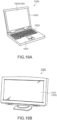
- the organic EL element 130 includes a reflection layer 102 provided on the element substrate 101, an insulating film 103, a pixel electrode 104, a counter electrode 105, and a functional layer 136 which is provided between the pixel electrode 104 and the counter electrode 105 and includes a light emitting layer 133.
- the pixel electrode 104 functions as an anode, and is provided for each of the sub-pixels 110R, 110G, and 110B, and is formed using a transparent conductive film of, for example, ITO (Indium Tin Oxide) or the like.
- ITO Indium Tin Oxide
- the reflection layer 102 provided in the lower layer of the pixel electrode 104 reflects light transmitted through the pixel electrode 104 having a light transmission property and emitted from the functional layer 136 back to the pixel electrode 104 side.
- the reflection layer 102 is formed using a metal having light reflectivity, for example, aluminum (Al), silver (Ag), or the like, or an alloy thereof, or the like. Therefore, in order to prevent an electrical short circuit between the reflection layer 102 and the pixel electrode 104, the insulating film 103 that covers the reflection layer 102 is provided.
- the insulating film 103 is formed using, for example, silicon oxide, silicon nitride, silicon oxynitride, or the like.
- the functional layer 136 is a layer obtained by stacking a hole injection layer 131, a hole transport layer 132, a light emitting layer 133, an electron transport layer 134, and an electron injection layer 135 in this order from the pixel electrode 104 side.
- the constituent material of the light emitting layer 133 is selected according to the light emission color, however, here, it is collectively referred to as "light emitting layer 133" regardless of the light emission color.
- the configuration of the functional layer 136 is not limited thereto, and an intermediate layer or the like which controls the transfer of a carrier (a hole or an electron) may be included in addition to these layers.
- the counter electrode 105 functions as a cathode, and is provided as a common electrode shared by the sub-pixels 110R, 110G, and 110B, and is formed using an alloy of Al (aluminum) or Ag (silver) and Mg (magnesium), or the like.
- a hole is injected as a carrier into the light emitting layer 133 from the pixel electrode 104 side as the anode, and an electron is injected as a carrier into the light emitting layer 133 from the counter electrode 105 side as the cathode.
- An exciton in a state where a hole and an electron are bound to each other by a Coulomb force
- the counter electrode 105 is configured to have a light transmission property, since the reflection layer 102 is included, it is possible to extract light emitted from the light emitting layer 133 from the counter electrode 105 side. Such a light emission type is referred to as "top emission type". Further, if the reflection layer 102 is eliminated and the counter electrode 105 is configured to have light reflectivity, it is also possible to provide a bottom emission type in which light emitted from the light emitting layer 133 is extracted from the element substrate 101 side. In this embodiment, a case where the organic EL device 100 is a top emission type device will be described below.
- the organic EL device 100 of this embodiment is an active driving type light emitting device which includes a pixel circuit capable of independently driving each organic EL element 130 for each of the sub-pixels 110R, 110G, and 110B on the element substrate 101. Since the pixel circuit can adopt a known configuration, the illustration of the pixel circuit is omitted in FIG. 2 .
- the organic EL device 100 in this embodiment has a partition wall 106 which overlaps with the outer edge of the pixel electrode 104 in the organic EL element 130 for each of the sub-pixels 110R, 110G, and 110B and forms an opening portion 106a on the pixel electrode 104.
- the functional layer 136 of the organic EL element 130 in this embodiment at least one layer of the hole injection layer 131, the hole transport layer 132, and the light emitting layer 133 constituting the functional layer 136 is formed by a liquid phase process.
- the liquid phase process is a method for forming each layer by applying a solution (functional layer forming composition) containing a component constituting each layer and a solvent to the opening portion 106a as a film forming region surrounded by the partition wall 106 and drying.
- a solution functional layer forming composition
- an inkjet method liquid droplet ejection method
- the cross-sectional shape of each layer constituting the functional layer 136 is flat.
- the functional layer forming composition of this embodiment is used such that a predetermined amount of the functional layer forming composition is uniformly applied to the opening portion 106a and dried so as to make the cross-sectional shape of each layer flat.
- the solvent configuration in the functional layer forming composition is devised. The detailed configuration of the functional layer forming composition will be described later.
- FIGS. 3(a) to 3(d) are schematic cross-sectional views showing a method for producing an organic EL element.
- a known method can be adopted, and therefore, a step of forming a partition wall and the subsequent steps will be described here.
- the method for producing the organic EL element 130 of this embodiment includes a partition wall formation step (Step S1), a surface treatment step (Step S2), a functional layer formation step (Step S3), and a counter electrode formation step (Step S4).
- a photosensitive resin layer is formed on the element substrate 101 on which the reflection layer 102 and the pixel electrode 104 are formed by, for example, applying a photosensitive resin material containing a liquid repellent material having liquid repellency to the functional layer forming composition to a thickness of 1 ⁇ m to 2 ⁇ m, followed by drying.
- a photosensitive resin material containing a liquid repellent material having liquid repellency to the functional layer forming composition to a thickness of 1 ⁇ m to 2 ⁇ m, followed by drying.
- the application method include a transfer method and a slit coating method.
- the liquid repellent material include fluorine compounds and siloxane-based compounds.
- the photosensitive resin material include negative polyfunctional acrylic resins.
- the thus formed photosensitive resin layer is exposed to light and developed using an exposure mask corresponding to the shape of the sub-pixels 110, whereby the partition wall 106 which overlaps with the outer edge of the pixel electrode 104, and also forms the opening portion 106a on the pixel electrode 104 is formed. Then, the process proceeds to Step S2.
- the element substrate 101 on which the partition wall 106 is formed is subjected to a surface treatment.
- the surface treatment step is performed for the purpose of removing unnecessary materials such as partition wall residues on the surface of the pixel electrode 104 so that the functional layer forming composition containing a functional layer forming material (solid component) wets and spreads uniformly in the opening portion 106a surrounded by the partition wall 106 when forming the hole injection layer 131, the hole transport layer 132, and the light emitting layer 133 constituting the functional layer 136 by an inkjet method (liquid droplet ejection method) in the subsequent step.
- an excimer UV (ultraviolet ray) treatment is performed as the surface treatment method.
- the surface treatment method is not limited to the excimer UV treatment and may be any as long as the surface of the pixel electrode 104 can be cleaned, and for example, a washing and drying step may be performed using a solvent. If the surface of the pixel electrode 104 is in a clean state, it is not necessary to perform the surface treatment step.
- the partition wall 106 is formed using a photosensitive resin material containing a liquid repellent material, however, the invention is not limited thereto, and after forming the partition wall 106 using a photosensitive resin material which does not contain a liquid repellent material, liquid repellency is imparted to the surface of the partition wall 106 by performing, for example, a plasma treatment using a fluorine-based treatment gas in Step S2, and thereafter, a surface treatment for making the surface of the pixel electrode 104 lyophilic may be performed by performing a plasma treatment using oxygen as a treatment gas. Then, the process proceeds to Step S3.
- a hole injection layer forming ink 50 as the functional layer forming composition containing a hole injection material is applied to the opening portion 106a.
- an inkjet method liquid droplet ejection method in which the hole injection layer forming ink 50 is ejected as a liquid droplet D from the nozzle 21 of the inkjet head 20 is used.
- the ejection amount of the liquid droplet D ejected from the inkjet head 20 can be controlled in picoliter (pl) order, and the liquid droplets D whose number is calculated by dividing a predetermined amount by the ejection amount of the liquid droplet D is ejected to the opening portion 106a.
- the ejected hole injection layer forming ink 50 rounds up in the opening portion 106a due to an interfacial surface tension between the ink and the partition wall 106, but never overflows.
- the concentration of the hole injection material in the hole injection layer forming ink 50 is adjusted in advance so that the predetermined amount does not cause overflowing of the ink from the opening portion 106a. Then, the process proceeds to the drying step.
- the drying step for example, decompression drying in which the element substrate 101 to which the hole injection layer forming ink 50 is applied is left under reduced pressure and dried by evaporating the solvent from the hole injection layer forming ink 50 is used (a decompression drying step). Thereafter, the ink is solidified by performing a firing treatment of heating under atmospheric pressure to, for example, 180°C for 30 minutes, whereby the hole injection layer 131 is formed as shown in FIG. 3(c) .
- the hole injection layer 131 is formed with a film thickness of about 10 nm to 30 nm, although not necessarily limited thereto in relation to the selection of the below-mentioned hole injection material or the other layers in the functional layer 136.
- the hole transport layer 132 is formed using a hole transport layer forming ink 60 as the functional layer forming composition containing a hole transport material.
- the method for forming the hole transport layer 132 is also performed using an inkjet method (liquid droplet ejection method) similarly to the hole injection layer 131. That is, a predetermined amount of the hole transport layer forming ink 60 is ejected as a liquid droplet D from the nozzle 21 of the inkjet head 20 to the opening portion 106a. Then, the hole transport layer forming ink 60 applied to the opening portion 106a is dried under reduced pressure.
- the hole transport layer 132 is formed with a film thickness of about 10 nm to 20 nm, although not necessarily limited thereto in relation to the selection of the below-mentioned hole transport material or the other layers in the functional layer 136. Further, the hole injection layer 131 and the hole transport layer 132 may be combined to form a hole injection transport layer in relation to the other layers in the functional layer 136.
- the light emitting layer 133 is formed using a light emitting layer forming ink 70 as the functional layer forming composition containing a light emitting layer forming material.
- the method for forming the light emitting layer 133 is also performed using an inkjet method (liquid droplet ejection method) similarly to the hole injection layer 131. That is, a predetermined amount of the light emitting layer forming ink 70 is ejected as a liquid droplet D from the nozzle 21 of the inkjet head 20 to the opening portion 106a. Then, the light emitting layer forming ink 70 applied to the opening portion 106a is dried under reduced pressure.
- the light emitting layer 133 is formed with a film thickness of about 60 nm to 80 nm, although not necessarily limited thereto in relation to the selection of the below-mentioned light emitting layer forming material or the other layers in the functional layer 136.
- An electron transport material constituting the electron transport layer 134 is not particularly limited, however, examples thereof include BAlq, 1,3,5-tri(5-(4-tert-butylphenyl)-1,3,4-oxadiazole) (OXD-1), BCP (Bathocuproine), 2-(4-biphenyl)-5-(4-tert-butylphenyl)-1,2,4-oxadiazole (PBD), 3-(4-biphenyl)-5-(4-tert-butylphenyl)-1,2,4-triazole (TAZ), 4,4'-bis(1,1-bis-diphenylethenyl)biphenyl (DPVBi), 2,5-bis(1-naphthyl)-1,3,4-oxadiazole (BND), 4,4'-bis(1,1-bis(4-methylphenyl)ethenyl
- BAlq 1,3,5-tri(5-(4-tert-butylphen
- Additional examples thereof include tris(8-quinolinolato)aluminum (Alq3), oxadiazole derivatives, oxazole derivatives, phenanthroline derivatives, anthraquinodimethane derivatives, benzoquinone derivatives, naphthoquinone derivatives, anthraquinone derivatives, tetracyanoanthraquinodimethane derivatives, fluorene derivatives, diphenyldicyanoethylene derivatives, diphenoquinone derivatives, and hydroxyquinoline derivatives.
- Alq3 tris(8-quinolinolato)aluminum
- oxadiazole derivatives oxadiazole derivatives
- oxazole derivatives oxazole derivatives
- phenanthroline derivatives anthraquinodimethane derivatives
- benzoquinone derivatives naphthoquinone derivatives
- anthraquinone derivatives tetracyan
- the electron transport layer 134 is formed with a film thickness of about 20 nm to 40 nm, although not necessarily limited thereto in relation to the selection of the above-mentioned electron transport material or the other layers in the functional layer 136. According to this, electrons injected from the counter electrode 105 as a cathode can be preferably transported to the light emitting layer 133. Incidentally, it is also possible to delete the electron transport layer 134 in relation to the other layers in the functional layer 136.
- the electron injection layer 135 is formed to cover the electron transport layer 134.
- An electron injection material constituting the electron injection layer 135 is not particularly limited, however, examples thereof include alkali metal compounds and alkaline earth metal compounds so that the electron injection layer 135 can be formed using a gas phase process such as a vacuum deposition method.
- alkali metal compounds examples include alkali metal salts such as LiF, Li 2 CO 3 , LiCl, NaF, Na 2 CO 3 , NaCl, CsF, Cs 2 CO 3 , and CsCl.
- alkaline earth metal compounds examples include alkaline earth metal salts such as CaF 2 , CaCO 3 , SrF 2 , SrCO 3 , BaF 2 , and BaCO 3 .
- alkali metal compounds and alkaline earth metal compounds it is possible to use one type or two or more types in combination.
- the film thickness of the electron injection layer 135 is not particularly limited, but is preferably about 0.01 nm or more and 10 nm or less, more preferably about 0.1 nm or more and 5 nm or less. According to this, electrons can be efficiently injected from the counter electrode 105 as a cathode to the electron transport layer 134.
- the counter electrode 105 is formed as a cathode to cover the electron injection layer 135. It is preferred to use a material with a low work function as the constituent material of the counter electrode 105, and, for example, Li, Mg, Ca, Sr, La, Ce, Er, Eu, Sc, Y, Yb, Ag, Cu, Al, Cs, Rb, Au, or an alloy containing any of these metals, or the like is used so that the counter electrode 105 can be formed using a gas phase process such as a vacuum deposition method, and among these, it is possible to use one type or two or more types in combination (for example, a stacked body of a plurality of layers, or the like).
- a gas phase process such as a vacuum deposition method
- the organic EL device 100 is a top emission type device
- a metal such as Mg, Al, Ag, or Au
- an alloy such as MgAg, MgAl, MgAu, or AlAg
- the film thickness of the counter electrode 105 in the top emission type device is not particularly limited, but is preferably about 1 nm or more and 50 nm or less, more preferably about 5 nm or more and 20 nm or less.
- the organic EL device 100 is a bottom emission type device
- a light transmission property is not required for the counter electrode 105. Therefore, for example, a metal or an alloy such as Al, Ag, AlAg, or AINd is preferably used. By using such a metal or an alloy as the constituent material of the counter electrode 105, the electron injection efficiency and stability of the counter electrode 105 can be improved.
- the film thickness of the counter electrode 105 in the bottom emission type device is not particularly limited, but is preferably about 50 nm or more and 1000 nm or less, more preferably about 100 nm or more and 500 nm or less.
- the light emitting function in the functional layer 136 of the organic EL element 130 formed by the above production method is impaired, and the luminous brightness is partially lowered, or a dark point (dark spot) which does not emit light is generated. There is also a concern that the emission lifetime is shortened. Therefore, in order to protect the organic EL element 130 from the entry of moisture, oxygen, or the like, it is preferred to cover the organic EL element 130 with a sealing layer (not shown).
- a sealing layer for example, an inorganic insulating material such as silicon oxynitride (SiON) with low permeability to water, oxygen, or the like can be used.
- the organic EL element 130 may be sealed by, for example, attaching a sealing substrate such as a transparent glass to the element substrate 101 on which the organic EL element 130 is formed through an adhesive.
- the hole injection layer 131, the hole transport layer 132, and the light emitting layer 133 in the functional layer 136 are formed by a liquid phase process (inkjet method), however, it is only necessary to form one of these layers by a liquid phase process (inkjet method), and the other layers may be formed by a gas phase process such as vacuum deposition.
- Preferred hole injection transport materials for forming the hole injection layer (HIL) 131 and the hole transport layer (HTL) 132 are not particularly limited, however, various types of p-type high-molecular weight materials and various types of p-type low-molecular weight materials can be used alone or in combination.
- Examples of the p-type high-molecular weight materials include aromatic amine-based compounds having an arylamine skeleton such as polyarylamines including poly(2,7-(9,9-di-n-octylfluorene)-(1,4-phenylene-((4-sec-butylphenyl)imino)-1,4-phenylene (TFB) and the like, polyfluorene derivatives (PF) having a fluorene skeleton such as a fluorene-bithiophene copolymer and polyfluorene derivatives (PF) having both of an arylamine skeleton and a fluorene skeleton such as a fluorene-arylamine copolymer, poly(N-vinylcarbazole) (PVK), polyvinyl pyrene, polyvinyl anthracene, polythiophene, polyalkylthiophene, polyhexylthi
- Such a p-type high-molecular weight material can also be used as a mixture with another compound.
- a mixture containing polythiophene, poly(3,4-ethylenedioxythiophene)/polystyrene sulfonic acid) (PEDOT/PSS), an electrically conductive polymer VERAZOL (registered trademark) manufactured by Soken Chemical & Engineering Co., Ltd. or the like, and ELsource (registered trademark) manufactured by Nissan Chemical Industries, Ltd. as polyaniline can be exemplified.
- p-type low-molecular weight materials include arylcycloalkane-based compounds such as 1,1-bis(4-di-para-tolylaminophenyl)cyclohexane and 1,1'-bis(4-di-para-tolylaminophenyl)-4-phenyl-cyclohexane (TAPC), arylamine-based compounds such as 4,4',4"-trimethyltriphenylamine, N,N'-diphenyl-N,N'-bis(3-methylphenyl)-1,1'-biphenyl-4,4'-diamine (TPD), N,N,N',N'-tetraphenyl-1,1'-biphenyl-4,4'-diamine, N,N'-diphenyl-N,N'-bis(3-methylphenyl)-1,1'-biphenyl-4,4'-diamine (TPD1), N,N'-diphenyl-N,
- stilbene-based compounds such as stilbene and 4-di-para-tolylaminostilbene
- oxazole-based compounds such as OxZ
- triphenylmethane-based compounds such as triphenylmethane
- pyrazoline-based compounds such as 1-phenyl-3-(para-dimethylaminophenyl)pyrazoline
- benzine(cyclohexadiene)-based compounds triazole-based compounds
- imidazole-based compounds such as imidazole
- oxadiazole-based compounds such as 1,3,4-o
- PDA-Si is used by adding a cationic polymerizable compound: xylene bisoxetane (ARONE OXETANE OXT-121, Toagosei Co., Ltd.) and a radical polymerization initiator: an aliphatic diacyl peroxide (PEROYL L, NOF Corporation) in order to achieve polymerization.
- a cationic polymerizable compound xylene bisoxetane
- PARONE OXETANE OXT-121 Toagosei Co., Ltd.
- a radical polymerization initiator an aliphatic diacyl peroxide (PEROYL L, NOF Corporation)
- EML material a light emitting material from which fluorescence or phosphorescence is obtained
- a red light emitting material is not particularly limited, and various types of red fluorescent materials and red phosphorescent materials can be used alone or two or more types thereof can be used in combination.
- the red fluorescent material is not particularly limited as long as it emits red fluorescence, and examples thereof include perylene derivatives, europium complexes, benzopyran derivatives, rhodamine derivatives, benzothioxanthene derivatives, porphyrin derivatives, nile red, 2-(1,1-dimethylethyl)-6-(2-(2,3,6,7-tetrahydro-1,1,7,7-tetramethyl-1H,5H-benzo(ij)quinolizin-9-yl)ethenyl)-4H-pyran-4H-ylidene)propanedinitrile (DCJTB), 4-(dicyanomethylene)-2-methyl-6-(p-dimethylaminostyryl)-4H-pyran (DCM), poly[2-methoxy-5-(2-ethylhexyloxy)-1,4-(1-cyanovinylenephenylene)], poly[ ⁇ 9,9-dihexyl-2,7-bis(
- the red phosphorescent material is not particularly limited as long as it emits red phosphorescence, and examples thereof include metal complexes such as complexes of iridium, ruthenium, platinum, osmium, rhenium, and palladium, and metal complexes in which at least one of the ligands of such a metal complex has a phenylpyridine skeleton, a bipyridyl skeleton, a porphyrin skeleton or the like.
- More specific examples thereof include tris(1-phenylisoquinoline)iridium, bis[2-(2'-benzo[4,5- ⁇ ]thienyl)pyridinato-N,C3']iridium (acetylacetonate) (Btp2lr(acac)), 2,3,7,8,12,13,17,18-octaethyl-12H,23H-porphyrin-platinum (II), fac-tris(2-phenyl)-bis(2-(2'-benzo[4,5- ⁇ ]thienyl)-pyridinato-N,C3')iridium (acetylacetonate) (Bt2lr(acac)), and bis(2-phenylpyridine)iridium (acetylacetonate).
- the red light emitting layer 133 may contain, in addition to the above-mentioned red light emitting material, a host material to which the red light emitting material is added as a guest material.
- the host material has a function to generate an exciton by recombining a hole and an electron with each other, and also to excite the red light emitting material by transferring the energy of the exciton to the red light emitting material (Forster transfer or Dexter transfer).
- the red light emitting material which is the guest material can be used by doping the host material with the red light emitting material as a dopant.
- Such a host material is not particularly limited as long as it has a function as described above for the red light emitting material to be used, however, in the case where the red light emitting material contains a red fluorescent material, examples thereof include acene derivatives (acene-based materials) such as naphthacene derivatives, naphthalene derivatives, and anthracene derivatives, distyrylarylene derivatives, perylene derivatives, distyrylbenzene derivatives, distyrylamine derivatives, quinolinolate-based metal complexes (BAql) such as tris(8-quinolinolato)aluminum complex (Alq3), triarylamine derivatives (TDAPB) such as triphenylamine tetramers, oxadiazole derivatives, silole derivatives (SimCP and UGH3), dicarbazole derivatives (CBP, mCP, CDBP, and DCB), oligothiophene derivatives, benzopyran
- the content (doping amount) of the red light emitting material in the red light emitting layer 133 is preferably from 0.01 to 10 wt%, more preferably from 0.1 to 5 wt%.
- a green light emitting material is not particularly limited, and examples thereof include various types of green fluorescent materials and green phosphorescent materials, and among these, it is possible to use one type or two or more types in combination.
- the green fluorescent material is not particularly limited as long as it emits green fluorescence, and examples thereof include coumarin derivatives, quinacridone and derivatives thereof, 9,10-bis[(9-ethyl-3-carbazole)-vinylenyl]-anthracene, poly(9,9-dihexyl-2,7-vinylenefluorenylene), poly[(9,9-dioctylfluorene-2,7-diyl)-co-(1,4-diphenylene-vinylene-2-methoxy-5- ⁇ 2-ethylhexyloxy ⁇ benzene)], poly[(9,9-dioctyl-2,7-divinylenefluorenylene)-alt-co-(2-methoxy-5-(2-ethoxylhexyloxy)-1,4-phenylene)], and poly[(9,9-dioctylfluorene-2,7-diyl)-alt
- the green phosphorescent material is not particularly limited as long as it emits green phosphorescence, and examples thereof include metal complexes such as complexes of iridium, ruthenium, platinum, osmium, rhenium, and palladium, and specific examples thereof include fac-tris(2-phenylpyridine)iridium (Ir(ppy)3), bis(2-phenylpyridinato-N,C2')iridium (acetylacetonate) (Ppy21r(acac)), and fac-tris[5-fluoro-2-(5-trifluoromethyl-2-pyridine)phenyl-C,N]iridium.
- metal complexes such as complexes of iridium, ruthenium, platinum, osmium, rhenium, and palladium
- specific examples thereof include fac-tris(2-phenylpyridine)iridium (Ir(ppy)3), bis(2-phenylpyridinato-N
- the green light emitting layer 133 may contain, in addition to the above-mentioned green light emitting material, a host material to which the green light emitting material is added as a guest material.
- the same host materials as those described for the above-mentioned red light emitting layer 133 can be used.
- Examples of a blue light emitting material include various types of blue fluorescent materials and blue phosphorescent materials, and among these, it is possible to use one type or two or more types in combination.
- the blue fluorescent material is not particularly limited as long as it emits blue fluorescence, and examples thereof include distyrylamine derivatives such as distyryldiamine-based compounds, fluoranthene derivatives, pyrene derivatives, perylene and perylene derivatives, anthracene derivatives, benzoxazole derivatives, benzothiazole derivatives, benzoimidazole derivatives, chrysene derivatives, phenanthrene derivatives, distyrylbenzene derivatives, tetraphenylbutadiene, and 4,4'-bis(9-ethyl-3-carbazovinylene)-1,1'-biphenyl (BCzVBi), poly[(9,9-dioctylfluorene-2,7-diyl)-co-(2,5-dimethoxybenzene-1,4-diyl)], poly[(9,9-dihexyloxyfluorene-2,7-diy
- the blue phosphorescent material is not particularly limited as long as it emits blue phosphorescence, and examples thereof include metal complexes such as complexes of iridium, ruthenium, platinum, osmium, rhenium, and palladium, and specific examples thereof include bis[4,6-difluorophenylpyridinato-N,C2']-picolinate-iridium (Flrpic), tris(1-phenyl-3-methylbenzimidazolin-2-ylidene-C,C2') (Ir(pmb)3), bis(2,4-difluorophenylpyridinato)(5-(pyridin-2-yl)-1H-tetrazole)iridium (FlrN4), tris[2-(2,4-difluorophenyl)pyridinato-N,C2']iridium, bis[2-(3,5-trifluoromethyl)pyridinato-N,C2
- the blue light emitting layer 133 may contain, in addition to the above-mentioned blue light emitting material, a host material to which the blue light emitting material is added as a guest material.
- the same host materials as those described for the above-mentioned red light emitting layer 133 can be used.
- the low-molecular weight substance refers to a substance having a molecular weight of less than 1000
- the high-molecular weight substance refers to a substance having a molecular weight of 1000 or more and having a repeated structure of a basic skeleton.
- the basic configuration of a preferred functional layer forming composition when forming each of the hole injection layer 131, the hole transport layer 132, and the light emitting layer 133 in the functional layer 136 of the organic EL element 130 of this embodiment by a liquid phase process is as follows.
- the functional layer forming composition includes a solid component for forming a functional layer, a first aromatic solvent having an electron withdrawing group, and a second aromatic solvent having an electron donating group, and in which the boiling point of the second aromatic solvent is higher than the boiling point of the first aromatic solvent.
- the solvents are selected and the content ratio is set in consideration that the functional layer forming composition can be stably ejected from a nozzle of an inkjet head (ejection stability) and the film flatness of the formed functional layer 136 can be obtained. Further, the solvents are selected and the content ratio is set so that desired element characteristics are obtained in the organic EL element 130 including the formed functional layer 136.
- the first aromatic solvent having an electron withdrawing group has an excellent dissolution property (is a good solvent) for a solid component (organic EL material) for forming a functional layer, and preferably has a boiling point (bp) of 200°C or higher in consideration of ejection stability.
- bp boiling point
- Specific examples thereof include nitrobenzene (bp: 210°C), 2,3-dimethylnitrobenzene (bp: 245°C), and 2,4-dimethylnitrobenzene (bp: 245°C), each of which has a nitro group (-NO 2 group) as the electron withdrawing group.
- the second aromatic solvent having an electron donating group is not necessarily a good solvent for a solid component (organic EL material) for forming a functional layer, and preferably has a boiling point (bp) of 250°C or higher which is higher than that of the first aromatic solvent.
- ⁇ , ⁇ ,4-trimethoxytoluene (bp: 253°C), diphenyl ether (bp: 258°C), 3-phenoxytoluene (bp: 272°C), benzylphenyl ether (bp: 288°C), aminobiphenyl (bp: 299°C), and diphenylamine (bp: 302°C), each of which has an alkoxy group (-OR group) or an amino group (-NH 3 group) as the electron donating group.
- R of the alkoxy group is not limited to an alkyl group, and may be a phenyl group.
- the boiling point (bp) thereof is preferably 350°C or lower.
- the method for producing a functional layer forming composition in this embodiment includes a step of dissolving a solid component for forming a functional layer in a first aromatic solvent having an electron withdrawing group, and a step of adding a second aromatic solvent having an electron donating group to the first aromatic solvent in which the solid component for forming the functional layer is dissolved.
- the first aromatic solvent shows a high dissolution property for the organic EL material which is the solid component for forming the functional layer, and therefore, a preparation work is completed in a shorter time when the solid component is dissolved in the first aromatic solvent than in the second aromatic solvent.
- the second aromatic solvent having a higher boiling point to the first aromatic solvent, it is possible to produce a functional layer forming composition which is chemically stable and is easy to handle.
- the functional layer forming composition is applied using an inkjet method, and therefore, for the sake of convenience of explanation, hereinafter, the functional layer forming composition is sometimes also simply referred to as "ink".
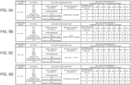
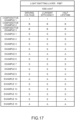
- FIGS. 5(a) to 5(d) and FIGS. 6(e) to 6(g) are tables of evaluation results showing a relationship between a solvent configuration and an ink ejection property in the case where a high-molecular weight hole injection transport material was used.
- FIGS. 7(a) to 7(d) and FIGS. 8(e) to 8(g) are tables of evaluation results showing a relationship between a solvent configuration and an ink ejection property in the case where a high-molecular weight light emitting material was used.
- the ejection amount (volume) of one liquid droplet ejected from the nozzle of the inkjet head is in picoliter (pl) order, and in order to accurately determine the ink ejection amount, in fact, for example, tens of thousands of liquid droplets were ejected, the weight of the ejected liquid droplets was measured, and the measured weight was divided by the number of ejection operations (tens of thousands), whereby the ink ejection amount per droplet was calculated.
- HIL high-molecular weight hole injection transport material
- a material was selected from the above-mentioned PVK, PF, PPV, PMPS, PTTA, poly[N,N'-bis(4-butylphenyl)-N,N'-bis(phenyl)-benzidine], and TFB.
- the first aromatic solvent A a solvent was selected from the above-mentioned nitrobenzene, 2,3-dimethylnitrobenzene, and 2,4-dimethylnitrobenzene.
- 2-methoxytoluene has a methoxy group (-OCH 3 group) which is an alkoxy group as the electron donating group.
- the evaluation was performed by setting the content ratio (A:B) % of the first aromatic solvent A to the second aromatic solvent B in the mixed solvent to seven ratios: 0:100, 10:90, 30:70, 50:50, 70:30, 90:10, and 100:0.
- the content ratio in this embodiment is expressed in volume (vol) %, however, the same evaluation results can be obtained also in the case where it is expressed in weight (wt) %.
- the ink ejection property (ejection stability) was evaluated as "C" in all the cases regardless of the content ratio in the mixed solvent.
- the ink ejection property (ejection stability) was evaluated as "C” when the content ratio in the mixed solvent was 0:100 and 10:90, and the ink ejection property (ejection stability) was evaluated as "B” when the content ratio (A:B) in the mixed solvent was 30:70, 50:50, 70:30, 90:10, and 100:0.
- the ink ejection property (ejection stability) was evaluated as "C" in all the cases regardless of the content ratio in the mixed solvent.
- the ink ejection property (ejection stability) was evaluated as "C” when the content ratio (A:B) in the mixed solvent was 0:100 and 10:90, and the ink ejection property (ejection stability) was evaluated as "B” when the content ratio (A:B) in the mixed solvent was 30:70, 50:50, 70:30, 90:10, and 100:0.
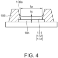
- FIG. 4 is a schematic cross-sectional view showing the film thickness of a central portion of a pixel in a functional layer
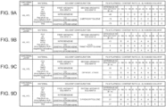
- FIGS. 9(a) to 9(d) and FIGS. 10(e) to 10(g) are tables of evaluation results showing a relationship between a solvent configuration and film flatness in the case where a high-molecular weight hole injection transport material was used.
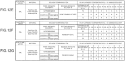
- FIGS. 11(a) to 11(d) and FIGS. 12(e) to 12(g) are tables of evaluation results showing a relationship between a solvent configuration and film flatness in the case where a high-molecular weight light emitting material was used.
- FIGS. 9(a) to 9(d) and FIGS. 10(e) to 10(g) are tables of evaluation results showing a relationship between a solvent configuration and film flatness in the case where a high-molecular weight light emitting material was used.
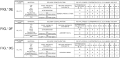
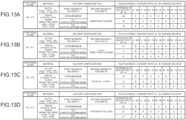
- FIGS. 13(a) to 13(d) and FIGS. 14(e) to 14(g) are tables of evaluation results showing a relationship between a solvent configuration and film flatness in the case where a low-molecular weight hole injection transport material was used.
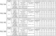
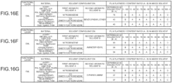
- FIGS. 15(a) to 15(d) and FIGS. 16(e) to 16(g) are tables of evaluation results showing a relationship between a solvent configuration and film flatness in the case where a low-molecular weight light emitting material was used.
- the film flatness of the formed functional layer is ensured. Further, it is considered that the film flatness is also affected by whether the solid component contained in the ink is a high-molecular weight material or a low-molecular weight material. Specifically, when the ink is applied to the opening portion 106a and dried, the pinning position (film fixed position) where the film formation starts on the side wall of the partition wall 106 varies depending on whether the solid component contained in the ink is a high-molecular weight material or a low-molecular weight material, and it is considered that this affects the film flatness after drying.
- the film thickness in a central portion of the pixel electrode 104 of the formed film is referred to as "intra-pixel central film thickness tc", and the average of the film thickness in a region in contact with the pixel electrode 104 is referred to as "intra-pixel average film thickness ta”.
- These film thicknesses can be measured by, for example, a probe-type measurement device.
- the shape of the cross section of the film after film formation is swollen or dented in a central portion of the pixel according to the progress of drying of the ink applied to the opening portion 106a or the above-mentioned pinning position. That is, the intra-pixel central film thickness tc varies.
- the film flatness in the case where the intra-pixel average film thickness ta is 0.9 times or more the intra-pixel central film thickness tc and less than 1.2 times the intra-pixel central film thickness tc, the film flatness is evaluated as "A (good)". At this time, the film flatness when minute irregularities are observed on the film surface due to the deposition of the solid component is evaluated as "B (having deposits)". In the case where the intra-pixel average film thickness ta is 1.2 times or more the intra-pixel central film thickness tc and less than 1.3 times the intra-pixel central film thickness tc, the film flatness is evaluated as "C (somewhat poor)".
- the film flatness is evaluated as "D (poor)". Further, in the case where the intra-pixel average film thickness ta is 1.3 times or more the intra-pixel central film thickness tc, and apparent irregularities are observed on the film surface due to the deposition of the solid component, the film flatness is evaluated as "E (poor and having deposits)". In the case where the film surface has apparent irregularities, when the organic EL element 130 is lit on, a variation in current flowing through the functional layer 136 in the pixel occurs to cause uneven brightness, and thus irregularities are recognized. Incidentally, the conditions for drying and firing of the ink applied to the opening portion 106a are as shown in the above-mentioned method for producing the organic EL element 130.
- HIL high-molecular weight hole injection transport material
- a material was selected from the above-mentioned PVK, PF, PPV, PMPS, PTTA, poly[N,N'-bis(4-butylphenyl)-N,N'-bis(phenyl)-benzidine], and TFB.
- the first aromatic solvent A a solvent was selected from the above-mentioned nitrobenzene, 2,3-dimethylnitrobenzene, and 2,4-dimethylnitrobenzene.
- 2-methoxytoluene has a methoxy group (-OCH 3 group) which is an alkoxy group as the electron donating group.
- the evaluation was performed by setting the content ratio (A:B) % of the first aromatic solvent A to the second aromatic solvent B in the mixed solvent to seven ratios: 0:100, 10:90, 30:70, 50:50, 70:30, 90:10, and 100:0. That is, the configuration of the ink is the same as in the case of the evaluation of the ejection stability described above.
- HIL low-molecular weight hole injection transport material
- a material was selected from the above-mentioned VB-TCA, CuPc, TAPC, TPD, ⁇ -NPD, m-MTDATA, PDA-Si, 2-TNATA, TCTA, TDAPB, spiro-TAD, DPPD, DTP, HTM1, HTM2, TPT1, and TPTE.
- the first aromatic solvent A a solvent was selected from the above-mentioned nitrobenzene, 2,3-dimethylnitrobenzene, and 2,4-dimethylnitrobenzene.
- 2-methoxytoluene has a methoxy group (-OCH 3 group) which is an alkoxy group as the electron donating group.
- a host material was selected from the above-mentioned CBP, BAIq, mCP, CDBP, DCB, PO6, SimCP, UGH3, and TDAPB, and a red dopant which is a red light emitting material (guest material) was selected from Bt2lr(acac), Btp2lr(acac), and PtOEP. Further, a green dopant which is a green light emitting material (guest material) was selected from Ir(ppy)3 and Ppy2lr(acac).
- a blue dopant which is a blue light emitting material (guest material) was selected from Flrpic, Ir(pmb)3, and FIrN4.
- the first aromatic solvent A and the second aromatic solvent B were selected in the same manner as in the case of the low-molecular weight hole injection transport material (HIL, HTL).
- the evaluation was performed by setting the content ratio (A:B) % of the first aromatic solvent A to the second aromatic solvent B in the mixed solvent to seven ratios: 0:100, 10:90, 30:70, 50:50, 70:30, 90:10, and 100:0. That is, the configuration of the ink is the same as in the case of the evaluation of the high-molecular weight material described above.
- FIGS. 13(b) to 13(d) and FIGS. 14(e) to 14(g) FIGS. 15(b) to 15(d) and FIGS. 16(e) to 16(g)
- the film flatness was evaluated as "A” in all the cases.
- the film flatness was evaluated as "B" when the content ratio (A:B) in the mixed solvent was 0:100, the film flatness was evaluated as "B", and when the content ratio (A:B) in the mixed solvent was 100:0, the film
- the film flatness was evaluated as "B"
- the content ratio (A:B) in the mixed solvent was 100:0
- the film flatness was evaluated as "C”. That is, even in the case where the solid component in the ink is a low-molecular weight material, the same evaluation of film flatness as in the case where the solid component in the ink is a high-molecular weight material was obtained.
- the second aromatic solvent B is evaporated prior to the first aromatic solvent A to increase the drying speed of the ink, and leveling at the time of film formation is not sufficiently performed, and therefore, the film flatness is deteriorated.
- the second aromatic solvent B in the case where the boiling point (bp) of a solvent selected as the second aromatic solvent B is 250°C or higher, in the step of drying the ink, the second aromatic solvent B remains even after the first aromatic solvent A is evaporated, and therefore, the drying speed of the ink is decreased so that leveling at the time of film formation is sufficiently performed and the film flatness is improved.
- the first aromatic solvent A which shows a high dissolution property for the solid component is not contained in the ink (in the case where the content ratio (A:B) in the mixed solvent is 0:100)
- the solid component in the process of drying the second aromatic solvent B having a poor dissolution property for the ink, the solid component is likely to be deposited.
- the boiling point of the first aromatic solvent A is 200°C or higher and the second aromatic solvent B having a boiling point of 250°C or higher is selected.
- the content ratio (A:B) of the first aromatic solvent A to the second aromatic solvent B in the mixed solvent is preferably between 10:90 and 90:10.
- the driving voltage is a DC voltage value at which the luminous brightness of the organic EL element 130 becomes a predetermined value, and a smaller driving voltage is preferred.
- the current efficiency is a value (cd (candela)/A (ampere)) obtained by dividing the luminous brightness of the organic EL element 130 by the value of a current flowing when the luminous brightness of the organic EL element 130 is set to a predetermined value, and a higher current efficiency is preferred.
- the half lifetime is an energization time (h) until the luminous brightness of the organic EL element 130 is halved from a predetermined value, and a longer half lifetime is preferred.
- the predetermined value of the luminous brightness is, for example, 1000 cd (candela)/m 2 (square meter).
- the organic EL element of Comparative Example 1 is configured such that the hole injection layer 131, the hole transport layer 132, and the light emitting layer 133 in the functional layer 136 are formed by an inkjet method using an ink which does not contain the second aromatic solvent B.
- nitrobenzene (bp: 210°C) was used as the first aromatic solvent A
- the hole injection layer 131 having a film thickness of 10 nm to 30 nm was formed using an ink in which VB-TCA serving as a hole injection material was dissolved in nitrobenzene.
- the hole transport layer 132 having a film thickness of 10 nm to 20 nm was formed using an ink in which TFB serving as a hole transport material was dissolved in nitrobenzene.
- the light emitting layer 133 having a film thickness of 60 nm to 80 nm was formed using an ink in which F8BT (Green-Poly-EM) serving as a light emitting material from which fluorescence is obtained was dissolved in nitrobenzene.
- F8BT Green-Poly-EM
- the configurations of the other electron transport layer 134 and electron injection layer 135 in the functional layer 136 are as described in the method for producing the organic EL element 130.
- the hole injection layer 131, the hole transport layer 132, and the light emitting layer 133 were formed using an ink containing a mixed solvent obtained by adding 2-methoxytoluene (bp: 170°C) as the second aromatic solvent B to nitrobenzene (bp: 210°C) as the first aromatic solvent A in which the solid component was dissolved.
- the layer constituent material and the film thickness of each layer are the same as those of Comparative Example 1.
- the content ratio (A:B) in the above mixed solvent is 50:50.
- the hole injection layer 131, the hole transport layer 132, and the light emitting layer 133 were formed using an ink containing a mixed solvent obtained by adding 1,3,5-triethylbenzene (bp: 215°C) as the second aromatic solvent B to nitrobenzene (bp: 210°C) as the first aromatic solvent A in which the solid component was dissolved.
- the layer constituent material and the film thickness of each layer are the same as those of Comparative Example 1.
- the content ratio (A:B) in the above mixed solvent is 60:40.
- the hole injection layer 131, the hole transport layer 132, and the light emitting layer 133 were formed using an ink containing a mixed solvent obtained by adding 3-phenoxytoluene (bp: 272°C) as the second aromatic solvent B to nitrobenzene (bp: 210°C) as the first aromatic solvent A in which the solid component was dissolved.
- the layer constituent material and the film thickness of each layer are the same as those of Comparative Example 1.
- the content ratio (A:B) in the above mixed solvent is 10:90.
- the hole injection layer 131, the hole transport layer 132, and the light emitting layer 133 were formed using an ink containing a mixed solvent obtained by adding 3-phenoxytoluene (bp: 272°C) as the second aromatic solvent B to nitrobenzene (bp: 210°C) as the first aromatic solvent A in which the solid component was dissolved.
- the layer constituent material and the film thickness of each layer are the same as those of Comparative Example 1.
- the content ratio (A:B) in the above mixed solvent is 30:70.
- the hole injection layer 131, the hole transport layer 132, and the light emitting layer 133 were formed using an ink containing a mixed solvent obtained by adding 3-phenoxytoluene (bp: 272°C) as the second aromatic solvent B to nitrobenzene (bp: 210°C) as the first aromatic solvent A in which the solid component was dissolved.
- the layer constituent material and the film thickness of each layer are the same as those of Comparative Example 1.
- the content ratio (A:B) in the above mixed solvent is 50:50.
- the hole injection layer 131, the hole transport layer 132, and the light emitting layer 133 were formed using an ink containing a mixed solvent obtained by adding 3-phenoxytoluene (bp: 272°C) as the second aromatic solvent B to nitrobenzene (bp: 210°C) as the first aromatic solvent A in which the solid component was dissolved.
- the layer constituent material and the film thickness of each layer are the same as those of Comparative Example 1.
- the content ratio (A:B) in the above mixed solvent is 70:30.
- the hole injection layer 131, the hole transport layer 132, and the light emitting layer 133 were formed using an ink containing a mixed solvent obtained by adding 3-phenoxytoluene (bp: 272°C) as the second aromatic solvent B to nitrobenzene (bp: 210°C) as the first aromatic solvent A in which the solid component was dissolved.
- the layer constituent material and the film thickness of each layer are the same as those of Comparative Example 1.
- the content ratio (A:B) in the above mixed solvent is 90:10.
- Example 1 to Example 5 the content ratio (A:B) in the mixed solvent containing nitrobenzene (bp: 210°C) as the first aromatic solvent A and 3-phenoxytoluene (bp: 272°C) as the second aromatic solvent B was made different.
- the hole injection layer 131, the hole transport layer 132, and the light emitting layer 133 were formed using an ink containing a mixed solvent obtained by adding 3-phenoxytoluene (bp: 272°C) as the second aromatic solvent B to 2,3-dimethylnitrobenzene (bp: 245°C) as the first aromatic solvent A in which the solid component was dissolved.
- the layer constituent material and the film thickness of each layer are the same as those of Comparative Example 1.
- the content ratio (A:B) in the above mixed solvent is 10:90.
- the hole injection layer 131, the hole transport layer 132, and the light emitting layer 133 were formed using an ink containing a mixed solvent obtained by adding 3-phenoxytoluene (bp: 272°C) as the second aromatic solvent B to 2,3-dimethylnitrobenzene (bp: 245°C) as the first aromatic solvent A in which the solid component was dissolved.
- the layer constituent material and the film thickness of each layer are the same as those of Comparative Example 1.
- the content ratio (A:B) in the above mixed solvent is 30:70.
- the hole injection layer 131, the hole transport layer 132, and the light emitting layer 133 were formed using an ink containing a mixed solvent obtained by adding 3-phenoxytoluene (bp: 272°C) as the second aromatic solvent B to 2,3-dimethylnitrobenzene (bp: 245°C) as the first aromatic solvent A in which the solid component was dissolved.
- the layer constituent material and the film thickness of each layer are the same as those of Comparative Example 1.
- the content ratio (A:B) in the above mixed solvent is 50:50.
- the hole injection layer 131, the hole transport layer 132, and the light emitting layer 133 were formed using an ink containing a mixed solvent obtained by adding 3-phenoxytoluene (bp: 272°C) as the second aromatic solvent B to 2,3-dimethylnitrobenzene (bp: 245°C) as the first aromatic solvent A in which the solid component was dissolved.
- the layer constituent material and the film thickness of each layer are the same as those of Comparative Example 1.
- the content ratio (A:B) in the above mixed solvent is 70:30.
- the hole injection layer 131, the hole transport layer 132, and the light emitting layer 133 were formed using an ink containing a mixed solvent obtained by adding 3-phenoxytoluene (bp: 272°C) as the second aromatic solvent B to 2,3-dimethylnitrobenzene (bp: 245°C) as the first aromatic solvent A in which the solid component was dissolved.
- the layer constituent material and the film thickness of each layer are the same as those of Comparative Example 1.
- the content ratio (A:B) in the above mixed solvent is 90:10.
- Example 6 the content ratio (A:B) in the mixed solvent containing 2,3-dimethylnitrobenzene (bp: 245°C) as the first aromatic solvent A and 3-phenoxytoluene (bp: 272°C) as the second aromatic solvent B was made different.
- the hole injection layer 131, the hole transport layer 132, and the light emitting layer 133 were formed using an ink containing a mixed solvent obtained by adding 3-phenoxytoluene (bp: 272°C) as the second aromatic solvent B to 2,4-dimethylnitrobenzene (bp: 245°C) as the first aromatic solvent A in which the solid component was dissolved.
- the layer constituent material and the film thickness of each layer are the same as those of Comparative Example 1.
- the content ratio (A:B) in the above mixed solvent is 10:90.
- the hole injection layer 131, the hole transport layer 132, and the light emitting layer 133 were formed using an ink containing a mixed solvent obtained by adding 3-phenoxytoluene (bp: 272°C) as the second aromatic solvent B to 2,4-dimethylnitrobenzene (bp: 245°C) as the first aromatic solvent A in which the solid component was dissolved.
- the layer constituent material and the film thickness of each layer are the same as those of Comparative Example 1.
- the content ratio (A:B) in the above mixed solvent is 30:70.
- the hole injection layer 131, the hole transport layer 132, and the light emitting layer 133 were formed using an ink containing a mixed solvent obtained by adding 3-phenoxytoluene (bp: 272°C) as the second aromatic solvent B to 2,4-dimethylnitrobenzene (bp: 245°C) as the first aromatic solvent A in which the solid component was dissolved.
- the layer constituent material and the film thickness of each layer are the same as those of Comparative Example 1.
- the content ratio (A:B) in the above mixed solvent is 50:50.
- the hole injection layer 131, the hole transport layer 132, and the light emitting layer 133 were formed using an ink containing a mixed solvent obtained by adding 3-phenoxytoluene (bp: 272°C) as the second aromatic solvent B to 2,4-dimethylnitrobenzene (bp: 245°C) as the first aromatic solvent A in which the solid component was dissolved.
- the layer constituent material and the film thickness of each layer are the same as those of Comparative Example 1.
- the content ratio (A:B) in the above mixed solvent is 70:30.
- the hole injection layer 131, the hole transport layer 132, and the light emitting layer 133 were formed using an ink containing a mixed solvent obtained by adding 3-phenoxytoluene (bp: 272°C) as the second aromatic solvent B to 2,4-dimethylnitrobenzene (bp: 245°C) as the first aromatic solvent A in which the solid component was dissolved.
- the layer constituent material and the film thickness of each layer are the same as those of Comparative Example 1.
- the content ratio (A:B) in the above mixed solvent is 90:10.
- Example 11 to Example 15 the content ratio (A:B) in the mixed solvent containing 2,4-dimethylnitrobenzene (bp: 245°C) as the first aromatic solvent A and 3-phenoxytoluene (bp: 272°C) as the second aromatic solvent B was made different.
- TDAPB TDAPB was used as a host material
- Ppy2lr serving as a light emitting material (guest material) from which phosphorescence is obtained
- F8BT light emitting material from which fluorescence is obtained
- the hole injection layer 131 having a film thickness of 10 nm to 30 nm was formed using an ink in which the second aromatic solvent B was not contained, and nitrobenzene (bp: 210°C) was used as the first aromatic solvent A, and VB-TCA serving as a hole injection material was dissolved in nitrobenzene.
- the hole transport layer 132 having a film thickness of 10 nm to 20 nm was formed using an ink in which TFB serving as a hole transport material was dissolved in nitrobenzene.
- the light emitting layer 133 having a film thickness of 60 nm to 80 nm was formed using an ink in which the above-mentioned light emitting material from which phosphorescence is obtained was dissolved in nitrobenzene.
- the configurations of the other electron transport layer 134 and electron injection layer 135 in the functional layer 136 are as described in the method for producing the organic EL element 130.
- the hole injection layer 131, the hole transport layer 132, and the light emitting layer 133 were formed using an ink containing a mixed solvent obtained by adding 2-methoxytoluene (bp: 170°C) as the second aromatic solvent B to nitrobenzene (bp: 210°C) as the first aromatic solvent A in which the solid component was dissolved.
- the layer constituent material and the film thickness of each layer are the same as those of Comparative Example 4.
- the content ratio (A:B) in the above mixed solvent is 50:50.
- the hole injection layer 131, the hole transport layer 132, and the light emitting layer 133 were formed using an ink containing a mixed solvent obtained by adding 1,3,5-triethylbenzene (bp: 215°C) as the second aromatic solvent B to nitrobenzene (bp: 210°C) as the first aromatic solvent A in which the solid component was dissolved.
- the layer constituent material and the film thickness of each layer are the same as those of Comparative Example 4.
- the content ratio (A:B) in the above mixed solvent is 60:40.
- the hole injection layer 131, the hole transport layer 132, and the light emitting layer 133 were formed using an ink containing a mixed solvent obtained by adding 3-phenoxytoluene (bp: 272°C) as the second aromatic solvent B to nitrobenzene (bp: 210°C) as the first aromatic solvent A in which the solid component was dissolved.
- the layer constituent material and the film thickness of each layer are the same as those of Comparative Example 4.
- the content ratio (A:B) in the above mixed solvent is 10:90.
- the hole injection layer 131, the hole transport layer 132, and the light emitting layer 133 were formed using an ink containing a mixed solvent obtained by adding 3-phenoxytoluene (bp: 272°C) as the second aromatic solvent B to nitrobenzene (bp: 210°C) as the first aromatic solvent A in which the solid component was dissolved.
- the layer constituent material and the film thickness of each layer are the same as those of Comparative Example 4.
- the content ratio (A:B) in the above mixed solvent is 30:70.
- the hole injection layer 131, the hole transport layer 132, and the light emitting layer 133 were formed using an ink containing a mixed solvent obtained by adding 3-phenoxytoluene (bp: 272°C) as the second aromatic solvent B to nitrobenzene (bp: 210°C) as the first aromatic solvent A in which the solid component was dissolved.
- the layer constituent material and the film thickness of each layer are the same as those of Comparative Example 4.
- the content ratio (A:B) in the above mixed solvent is 50:50.
- the hole injection layer 131, the hole transport layer 132, and the light emitting layer 133 were formed using an ink containing a mixed solvent obtained by adding 3-phenoxytoluene (bp: 272°C) as the second aromatic solvent B to nitrobenzene (bp: 210°C) as the first aromatic solvent A in which the solid component was dissolved.
- the layer constituent material and the film thickness of each layer are the same as those of Comparative Example 4.
- the content ratio (A:B) in the above mixed solvent is 70:30.
- the hole injection layer 131, the hole transport layer 132, and the light emitting layer 133 were formed using an ink containing a mixed solvent obtained by adding 3-phenoxytoluene (bp: 272°C) as the second aromatic solvent B to nitrobenzene (bp: 210°C) as the first aromatic solvent A in which the solid component was dissolved.
- the layer constituent material and the film thickness of each layer are the same as those of Comparative Example 4.
- the content ratio (A:B) in the above mixed solvent is 90:10.
- the hole injection layer 131, the hole transport layer 132, and the light emitting layer 133 were formed using an ink containing a mixed solvent obtained by adding 3-phenoxytoluene (bp: 272°C) as the second aromatic solvent B to 2,3-dimethylnitrobenzene (bp: 245°C) as the first aromatic solvent A in which the solid component was dissolved.
- the layer constituent material and the film thickness of each layer are the same as those of Comparative Example 4.
- the content ratio (A:B) in the above mixed solvent is 10:90.
- the hole injection layer 131, the hole transport layer 132, and the light emitting layer 133 were formed using an ink containing a mixed solvent obtained by adding 3-phenoxytoluene (bp: 272°C) as the second aromatic solvent B to 2,3-dimethylnitrobenzene (bp: 245°C) as the first aromatic solvent A in which the solid component was dissolved.
- the layer constituent material and the film thickness of each layer are the same as those of Comparative Example 4.
- the content ratio (A:B) in the above mixed solvent is 30:70.
- the hole injection layer 131, the hole transport layer 132, and the light emitting layer 133 were formed using an ink containing a mixed solvent obtained by adding 3-phenoxytoluene (bp: 272°C) as the second aromatic solvent B to 2,3-dimethylnitrobenzene (bp: 245°C) as the first aromatic solvent A in which the solid component was dissolved.
- the layer constituent material and the film thickness of each layer are the same as those of Comparative Example 4.
- the content ratio (A:B) in the above mixed solvent is 50:50.
- the hole injection layer 131, the hole transport layer 132, and the light emitting layer 133 were formed using an ink containing a mixed solvent obtained by adding 3-phenoxytoluene (bp: 272°C) as the second aromatic solvent B to 2,3-dimethylnitrobenzene (bp: 245°C) as the first aromatic solvent A in which the solid component was dissolved.
- the layer constituent material and the film thickness of each layer are the same as those of Comparative Example 4.
- the content ratio (A:B) in the above mixed solvent is 70:30.
- the hole injection layer 131, the hole transport layer 132, and the light emitting layer 133 were formed using an ink containing a mixed solvent obtained by adding 3-phenoxytoluene (bp: 272°C) as the second aromatic solvent B to 2,3-dimethylnitrobenzene (bp: 245°C) as the first aromatic solvent A in which the solid component was dissolved.
- the layer constituent material and the film thickness of each layer are the same as those of Comparative Example 4.
- the content ratio (A:B) in the above mixed solvent is 90:10.
- the hole injection layer 131, the hole transport layer 132, and the light emitting layer 133 were formed using an ink containing a mixed solvent obtained by adding 3-phenoxytoluene (bp: 272°C) as the second aromatic solvent B to 2,4-dimethylnitrobenzene (bp: 245°C) as the first aromatic solvent A in which the solid component was dissolved.
- the layer constituent material and the film thickness of each layer are the same as those of Comparative Example 4.
- the content ratio (A:B) in the above mixed solvent is 10:90.
- the hole injection layer 131, the hole transport layer 132, and the light emitting layer 133 were formed using an ink containing a mixed solvent obtained by adding 3-phenoxytoluene (bp: 272°C) as the second aromatic solvent B to 2,4-dimethylnitrobenzene (bp: 245°C) as the first aromatic solvent A in which the solid component was dissolved.
- the layer constituent material and the film thickness of each layer are the same as those of Comparative Example 4.
- the content ratio (A:B) in the above mixed solvent is 30:70.
- the hole injection layer 131, the hole transport layer 132, and the light emitting layer 133 were formed using an ink containing a mixed solvent obtained by adding 3-phenoxytoluene (bp: 272°C) as the second aromatic solvent B to 2,4-dimethylnitrobenzene (bp: 245°C) as the first aromatic solvent A in which the solid component was dissolved.
- the layer constituent material and the film thickness of each layer are the same as those of Comparative Example 4.
- the content ratio (A:B) in the above mixed solvent is 50:50.
- the hole injection layer 131, the hole transport layer 132, and the light emitting layer 133 were formed using an ink containing a mixed solvent obtained by adding 3-phenoxytoluene (bp: 272°C) as the second aromatic solvent B to 2,4-dimethylnitrobenzene (bp: 245°C) as the first aromatic solvent A in which the solid component was dissolved.
- the layer constituent material and the film thickness of each layer are the same as those of Comparative Example 4.
- the content ratio (A:B) in the above mixed solvent is 70:30.
- the hole injection layer 131, the hole transport layer 132, and the light emitting layer 133 were formed using an ink containing a mixed solvent obtained by adding 3-phenoxytoluene (bp: 272°C) as the second aromatic solvent B to 2,4-dimethylnitrobenzene (bp: 245°C) as the first aromatic solvent A in which the solid component was dissolved.
- the layer constituent material and the film thickness of each layer are the same as those of Comparative Example 4.
- the content ratio (A:B) in the above mixed solvent is 90:10.
- the driving voltage of Comparative Example 4 is taken as “1", and a case where the driving voltage of each of the other Comparative Examples 5 and 6, and Example 16 to Example 30 is smaller than 0.9 is evaluated as “S (superior)", 0.9 or more and less than 0.95 is evaluated as "A (good)”, 0.95 or more and less than 1.05 is evaluated as “B (somewhat poor)”, and 1.05 or more is evaluated as “C (poor)”.
- the current efficiency of Comparative Example 1 is taken as “1", and a case where the current efficiency of each of the other Comparative Examples 2 and 3, and Example 1 to Example 15 is larger than 1.1 is evaluated as “S (superior)", 1.05 or more and less than 1.1 is evaluated as “A (good)”, 0.95 or more and less than 1.05 is evaluated as “B (somewhat poor)”, and less than 0.95 is evaluated as “C (poor)”.
- Comparative Example 4 is taken as “1"
- a case where the current efficiency of each of the other Comparative Examples 5 and 6, and Example 16 to Example 30 is larger than 1.1 is evaluated as “S (superior)”
- 1.05 or more and less than 1.1 is evaluated as "A (good)”
- 0.95 or more and less than 1.05 is evaluated as “B (somewhat poor)”
- less than 0.95 is evaluated as "C (poor)”.
- the half lifetime of Comparative Example 1 is taken as “1", and a case where the half lifetime of each of the other Comparative Examples 2 and 3, and Example 1 to Example 15 is larger than 1.5 is evaluated as “S (superior)", 1.0 or more and less than 1.5 is evaluated as "A (good)”, 0.9 or more and less than 1.0 is evaluated as “B (somewhat poor)”, and less than 0.9 is evaluated as “C (poor)”.
- Comparative Example 4 is taken as “1"
- a case where the half lifetime of each of the other Comparative Examples 5 and 6, and Example 16 to Example 30 is larger than 1.5 is evaluated as “S (superior)”
- 1.0 or more and less than 1.5 is evaluated as "A (good)”
- 0.9 or more and less than 1.0 is evaluated as "B (somewhat poor)”
- less than 0.9 is evaluated as "C (poor)”.
- FIG. 17 is a table showing the evaluation results of the element characteristics of the organic EL elements of Comparative Example 1 to Comparative Example 3 and Example 1 to Example 15, and FIG. 18 is a table showing the evaluation results of the element characteristics of the organic EL elements of Comparative Example 4 to Comparative Example 6 and Example 16 to Example 30.
- Example 1 to Example 3 Example 6 to Example 8, and Example 11 to Example 13, in which the content ratio (A:B) of the first aromatic solvent A to the second aromatic solvent B in the mixed solvent was in the range of 10:90 to 50:50, the driving voltage, current efficiency, and half lifetime were all evaluated as "S (superior)".
- Example 4 Example 9, and Example 14, in which the content ratio (A:B) in the mixed solvent was 70:30, the driving voltage and current efficiency were evaluated as "S (superior)", and the half lifetime was evaluated as "A (good)”.
- Example 5 Example 10, and Example 15, in which the content ratio (A:B) in the mixed solvent was 90:10, the element characteristics were all evaluated as "A (good)”.
- Example 19 Example 24, and Example 29, in which the content ratio (A:B) in the mixed solvent was 70:30, the driving voltage and current efficiency were evaluated as "S (superior)", and the half lifetime was evaluated as "A (good)”.
- Example 20 Example 25, and Example 30 in which the content ratio (A:B) in the mixed solvent was 90:10 the element characteristics were all evaluated as "A (good)".
- the element characteristics are improved as compared with those in Comparative Examples in any combination of the solvents as long as the content ratio (A:B) of the first aromatic solvent A to the second aromatic solvent B in the mixed solvent is in the range of 10:90 to 90:10. Further, in Examples in which the content ratio (A:B) in the mixed solvent was 10:90, 30:70, or 50:50, that is, in the case where the content ratio of the second aromatic solvent B is equal to or larger than the content ratio of the first aromatic solvent A, more favorable evaluation of the element characteristics was obtained.
- the first aromatic solvent A having an electron withdrawing property due to an interaction (attractive force) between the first aromatic solvent A having an electron withdrawing property and the second aromatic solvent B having an electron donating property, the first aromatic solvent A having a low boiling point also evaporates simultaneously with the evaporation of the second aromatic solvent B having a high boiling point when a film is formed by drying and firing the ink. Therefore, the residual first aromatic solvent A having an electron withdrawing property in the film after film formation can be reduced.
- a functional layer forming composition (ink) capable of obtaining desired excellent element characteristics by preventing the first aromatic solvent A having an electron withdrawing property from affecting the element characteristics by remaining in the film after film formation.
- Comparative Example 2 the reason why the element characteristics of Comparative Example 2 are inferior to those of Comparative Example 1 is considered that by including 2-methoxytoluene having a lower boiling point than nitrobenzene in the ink, the drying speed of the ink is increased, and therefore, the film flatness is decreased, and nitrobenzene remains in the film and affects the element characteristics.
- the reason why the element characteristics of Comparative Example 5 are inferior to those of Comparative Example 4 is the same as described above.
- nitrobenzene, 2,3-dimethylnitrobenzene, and 2,4-dimethylnitrobenzene are exemplified, however, as the electron withdrawing group, other than a nitro group (-NO 2 group), a cyano group (-NH 3 group) can be used in examples not forming part of the claimed invention.
- the effect of the interaction is considered to be smaller in the case of a nitro group than in the case of a cyano group.
- a halogen group (-F (a fluoro group), -Cl (a chloro group), -Br (a bromo group), or -I (an iodo group) can be used in examples not forming part of the claimed invention.
- a halogen group has a stronger electron withdrawing property than a nitro group, and when a solvent having a halogen group remains in the functional layer, due to an interaction between the organic EL material and the halogen group, the element characteristics of the organic EL element are significantly deteriorated.
- the first aromatic solvent A having a nitro group as the electron withdrawing group shows a relatively low reactivity with the organic EL material.
- the second aromatic solvent B having an alkoxy group or an amino group as the electron donating group shows little reactivity with the organic EL material.
- the invention is not limited thereto, and a plurality of types of solvents may be selected for each solvent.
- the mixed solvent is not limited to those constituted by the first aromatic solvent A and the second aromatic solvent B, and for example, in order to adjust the viscosity or surface tension of the ink, another aromatic solvent, a surfactant, or the like, having a low reactivity with the organic EL material may be contained.
- the functional layer forming composition (ink) of this embodiment is favorable as a composition to be used when at least one layer in the functional layer is formed using an inkjet method, but the functional layer forming composition can also be applied to, for example, a liquid phase process such as a constant amount ejection method, a spin coating method, or a spray coating method, other than the inkjet method.
- FIG. 19(a) is a schematic view showing a notebook-type personal computer which is one example of the electronic apparatus
- FIG. 19(b) is a schematic view showing a thin-screen television (TV) which is one example of the electronic apparatus.
- TV thin-screen television
- a personal computer 1000 as the electronic apparatus is constituted by a main body part 1001 provided with a keyboard 1002 and a display unit 1003 provided with a display part 1004, and the display unit 1003 is supported rotatably with respect to the main body part 1001 through a hinge structure part.
- the organic EL device 100 of the above-mentioned first embodiment is mounted on the display part 1004.
- the organic EL device 100 of the above-mentioned first embodiment is mounted on a display part 1101.
- the organic EL element 130 provided in each of the sub-pixels 110R, 110G, and 110B of the organic EL device 100 at least one layer of the hole injection layer 131, the hole transport layer 132, and the light emitting layer 133 in the functional layer 136 is formed by a liquid phase process (inkjet method) using the functional layer forming composition of the above-mentioned first embodiment. Therefore, the film flatness in the functional layer 136 is ensured, and the organic EL device 100 including the organic EL element 130 having excellent element characteristics is produced. That is, the personal computer 1000 or the thin-screen TV 1100 having excellent display quality and reliable quality can be provided.
- the electronic apparatus in which the organic EL device 100 is mounted is not limited to the above-mentioned personal computer 1000 and thin-screen TV 1100.
- electronic apparatuses having a display part such as a portable information terminal such as a smartphone or a POS, a navigator, a viewer, a digital camera, and a monitor direct view-type video tape recorder can be exemplified.
- the organic EL device 100 is not limited to those constituting a display part, and may be a lighting device or a light exposure device which exposes a photosensitive material to light.
- the organic EL device 100 include the organic EL element 130 having the functional layer 136 formed using the functional layer forming composition of the invention in any of the sub-pixels 110R, 110G, and 110B.
- the organic EL element 130 having the functional layer 136 formed using the functional layer forming composition is included, and in the subpixel 110B, the organic EL element 130 having the functional layer 136 formed by a gas phase process may be included.
- the functional layer forming composition of the invention is not limited to being used in the formation of the functional layer 136 including the light emitting layer.
- a solid component (organic material) which is a solute may be a circuit element forming material of a semiconductor layer or the like constituting an organic transistor.
- hole injection layer forming ink as functional layer forming composition 60: hole transport layer forming ink as functional layer forming composition
- 70 light emitting layer forming ink as functional layer forming composition
- 100 organic EL device
- 104 pixel electrode
- 105 counter electrode
- 106a opening portion as film forming region
- 130 organic EL element
- 133 light emitting layer
- 136 functional layer
- 1000 personal computer as electronic apparatus
- 1100 thin-screen television (TV)
Landscapes
- Engineering & Computer Science (AREA)
- Chemical & Material Sciences (AREA)
- Materials Engineering (AREA)
- Manufacturing & Machinery (AREA)
- Physics & Mathematics (AREA)
- Spectroscopy & Molecular Physics (AREA)
- Life Sciences & Earth Sciences (AREA)
- Wood Science & Technology (AREA)
- Organic Chemistry (AREA)
- Electroluminescent Light Sources (AREA)
Applications Claiming Priority (2)
| Application Number | Priority Date | Filing Date | Title |
|---|---|---|---|
| JP2015062200A JP6550830B2 (ja) | 2015-03-25 | 2015-03-25 | 機能層形成用組成物、機能層形成用組成物の製造方法、有機el素子の製造方法、有機el装置、電子機器 |
| PCT/JP2016/001031 WO2016152028A1 (ja) | 2015-03-25 | 2016-02-25 | 機能層形成用組成物、機能層形成用組成物の製造方法、有機el素子の製造方法、有機el装置、電子機器 |
Publications (3)
| Publication Number | Publication Date |
|---|---|
| EP3276696A1 EP3276696A1 (en) | 2018-01-31 |
| EP3276696A4 EP3276696A4 (en) | 2018-11-21 |
| EP3276696B1 true EP3276696B1 (en) | 2023-10-11 |
Family
ID=56977158
Family Applications (1)
| Application Number | Title | Priority Date | Filing Date |
|---|---|---|---|
| EP16767940.6A Active EP3276696B1 (en) | 2015-03-25 | 2016-02-25 | Functional layer forming composition and method for manufacturing the same |
Country Status (7)
Families Citing this family (10)
| Publication number | Priority date | Publication date | Assignee | Title |
|---|---|---|---|---|
| WO2017102052A1 (en) | 2015-12-16 | 2017-06-22 | Merck Patent Gmbh | Formulations containing a solid solvent |
| JP7048250B2 (ja) * | 2017-10-19 | 2022-04-05 | 住友化学株式会社 | 有機電子デバイスの製造方法 |
| JP7158157B2 (ja) * | 2018-02-23 | 2022-10-21 | 東ソー株式会社 | 有機半導体インキ、それを用いた有機薄膜の製造方法 |
| CN108400259B (zh) | 2018-03-20 | 2020-05-01 | 京东方科技集团股份有限公司 | Oled器件的制备方法及显示面板的制备方法 |
| CN108281474B (zh) * | 2018-03-28 | 2019-05-10 | 京东方科技集团股份有限公司 | 有机发光显示面板及其制作方法、显示装置 |
| JP6657487B1 (ja) * | 2018-06-12 | 2020-03-04 | 住友化学株式会社 | 有機エレクトロルミネッセンス素子 |
| CN110165055B (zh) * | 2018-09-20 | 2021-12-21 | 合肥鑫晟光电科技有限公司 | 有机薄膜图案的制作方法及有机薄膜图案、阵列基板及显示装置 |
| KR102217266B1 (ko) | 2018-09-28 | 2021-02-17 | 주식회사 엘지화학 | 유기 발광 소자용 잉크 조성물 |
| CN112930606A (zh) * | 2018-11-06 | 2021-06-08 | 默克专利有限公司 | 用于形成电子器件的有机元件的方法 |
| KR20230134010A (ko) | 2022-03-10 | 2023-09-20 | 삼성디스플레이 주식회사 | 표시 패널의 제조 방법 |
Family Cites Families (26)
| Publication number | Priority date | Publication date | Assignee | Title |
|---|---|---|---|---|
| JPS62181234A (ja) * | 1986-02-05 | 1987-08-08 | Ihara Nikkei Kagaku Kogyo Kk | イソフタル酸ジクロリドの製造方法 |
| US6582504B1 (en) | 1999-11-24 | 2003-06-24 | Sharp Kabushiki Kaisha | Coating liquid for forming organic EL element |
| JP3836282B2 (ja) | 1999-11-24 | 2006-10-25 | シャープ株式会社 | 有機el用塗液及び有機el素子並びにその製造方法。 |
| JP2001279134A (ja) * | 2000-03-31 | 2001-10-10 | Seiko Epson Corp | 吐出組成物及び機能膜作製法 |
| JPWO2002012208A1 (ja) | 2000-08-04 | 2004-01-15 | タイホー工業株式会社 | ナイルレッド系赤色発光化合物、その製造方法及びそれを利用した発光素子 |
| WO2004000779A1 (ja) * | 2002-06-20 | 2003-12-31 | Sankio Chemical Co., Ltd. | フェニルオキソカルボン酸エステル誘導体の製造方法 |
| JP4515738B2 (ja) * | 2003-09-30 | 2010-08-04 | セイコーエプソン株式会社 | インク組成物 |
| DE102004023276A1 (de) * | 2004-05-11 | 2005-12-01 | Covion Organic Semiconductors Gmbh | Lösungen organischer Halbleiter |
| JP4701635B2 (ja) * | 2004-05-28 | 2011-06-15 | セイコーエプソン株式会社 | インク組成物、それを用いたインクジェット記録方法および記録物 |
| EP1758172A1 (en) * | 2004-06-10 | 2007-02-28 | Konica Minolta Holdings, Inc. | Organic semiconductor thin film, organic semiconductor device, organic thin film transistor, and organic electro-luminescence element |
| US20070153371A1 (en) * | 2005-12-30 | 2007-07-05 | Samsung Electronics Co., Ltd. | Display device, method of manufacturing the same, and composition for use in manufacturing the same |
| JP4887848B2 (ja) * | 2006-03-15 | 2012-02-29 | セイコーエプソン株式会社 | 回路基板、電気光学装置および電子機器 |
| JP5504585B2 (ja) * | 2007-06-29 | 2014-05-28 | 住友化学株式会社 | 重合性化合物および光学フィルム |
| JP5259139B2 (ja) * | 2007-08-31 | 2013-08-07 | 三菱化学株式会社 | 有機電界発光素子用組成物、有機電界発光素子および有機電界発光素子の製造方法 |
| TW200930467A (en) * | 2007-11-16 | 2009-07-16 | Sumitomo Chemical Co | Coating liquid for use in a coating method by delivering the coating liquid through a slit-shaped delivery port |
| CN101240117B (zh) * | 2008-02-04 | 2010-11-10 | 中国科学院长春应用化学研究所 | 纯有机染料和由其制备的染料敏化太阳能电池 |
| US20120025177A1 (en) * | 2009-02-06 | 2012-02-02 | Solvay Sa | Phosphorescent light-emitting iridium complex containing pyridyltriazole ligand |
| JP2010209317A (ja) | 2009-02-10 | 2010-09-24 | Mitsubishi Chemicals Corp | 金属錯体、有機電界発光素子用組成物および有機電界発光素子 |
| CN101885704A (zh) * | 2009-05-12 | 2010-11-17 | 北京大学 | 一种电子传输材料及其有机电致发光器件 |
| US20110057151A1 (en) * | 2009-09-10 | 2011-03-10 | Add-Vision, Inc. | Ionic salt combinations in polymer electroluminescent inks |
| US8652354B2 (en) | 2009-09-10 | 2014-02-18 | Sumitomo Chemical Co. Ltd. | Organic additives for improved lifetimes in organic and solution processible electronic devices |
| JP5463897B2 (ja) | 2009-12-18 | 2014-04-09 | コニカミノルタ株式会社 | 有機エレクトロルミネッセンス素子、有機エレクトロルミネッセンス素子材料、表示装置及び照明装置 |
| JP5573697B2 (ja) | 2011-01-21 | 2014-08-20 | 三菱化学株式会社 | 重合体、有機電界発光素子材料、有機電界発光素子用組成物、有機電界発光素子、有機el表示装置及び有機el照明 |
| US9293711B2 (en) * | 2012-08-09 | 2016-03-22 | Polyera Corporation | Organic semiconductor formulations |
| KR20140087250A (ko) * | 2012-12-28 | 2014-07-09 | 주식회사 두산 | 유기 전자 소자용 잉크 조성물 및 이를 이용하는 유기 전자 소자 |
| JP6201538B2 (ja) * | 2013-09-03 | 2017-09-27 | セイコーエプソン株式会社 | 機能層形成用インクの製造方法、有機el素子の製造方法 |
-
2015
- 2015-03-25 JP JP2015062200A patent/JP6550830B2/ja active Active
-
2016
- 2016-02-25 EP EP16767940.6A patent/EP3276696B1/en active Active
- 2016-02-25 WO PCT/JP2016/001031 patent/WO2016152028A1/ja active Application Filing
- 2016-02-25 CN CN201680017371.8A patent/CN107431137B/zh active Active
- 2016-02-25 KR KR1020177025597A patent/KR101953592B1/ko active Active
- 2016-02-25 US US15/556,583 patent/US10079342B2/en active Active
- 2016-03-22 TW TW105108883A patent/TWI699410B/zh active
Also Published As
| Publication number | Publication date |
|---|---|
| EP3276696A1 (en) | 2018-01-31 |
| CN107431137B (zh) | 2020-02-28 |
| JP2016181648A (ja) | 2016-10-13 |
| TWI699410B (zh) | 2020-07-21 |
| KR20170110722A (ko) | 2017-10-11 |
| TW201641620A (zh) | 2016-12-01 |
| EP3276696A4 (en) | 2018-11-21 |
| WO2016152028A1 (ja) | 2016-09-29 |
| CN107431137A (zh) | 2017-12-01 |
| KR101953592B1 (ko) | 2019-03-04 |
| US10079342B2 (en) | 2018-09-18 |
| US20180062078A1 (en) | 2018-03-01 |
| JP6550830B2 (ja) | 2019-07-31 |
Similar Documents
| Publication | Publication Date | Title |
|---|---|---|
| EP3276696B1 (en) | Functional layer forming composition and method for manufacturing the same | |
| CN104946006B (zh) | 功能层形成用油墨、发光元件的制造方法、发光装置、电子设备 | |
| EP3168269B1 (en) | Ink composition | |
| US10717886B2 (en) | Ink composition, method for producing organic semiconductor element, organic semiconductor device, and method for producing optical element | |
| US10526500B2 (en) | Film-forming ink, film formation method, device with film, and electronic apparatus | |
| US10167403B2 (en) | Ink, ink container, and method for producing functional element | |
| JP2017022068A (ja) | 有機el素子の製造方法、有機el素子の製造装置、電気光学装置および電子機器 | |
| JP2010209143A (ja) | 有機電界発光素子用組成物、有機電界発光素子、有機elディスプレイおよび有機el照明 | |
| JP2017004782A (ja) | 有機el素子の製造方法、電気光学装置、電子機器 | |
| JP2017010633A (ja) | 有機el素子の製造方法、電気光学装置、および電子機器 |
Legal Events
| Date | Code | Title | Description |
|---|---|---|---|
| STAA | Information on the status of an ep patent application or granted ep patent |
Free format text: STATUS: THE INTERNATIONAL PUBLICATION HAS BEEN MADE |
|
| PUAI | Public reference made under article 153(3) epc to a published international application that has entered the european phase |
Free format text: ORIGINAL CODE: 0009012 |
|
| STAA | Information on the status of an ep patent application or granted ep patent |
Free format text: STATUS: REQUEST FOR EXAMINATION WAS MADE |
|
| 17P | Request for examination filed |
Effective date: 20171025 |
|
| AK | Designated contracting states |
Kind code of ref document: A1 Designated state(s): AL AT BE BG CH CY CZ DE DK EE ES FI FR GB GR HR HU IE IS IT LI LT LU LV MC MK MT NL NO PL PT RO RS SE SI SK SM TR |
|
| AX | Request for extension of the european patent |
Extension state: BA ME |
|
| DAV | Request for validation of the european patent (deleted) | ||
| DAX | Request for extension of the european patent (deleted) | ||
| A4 | Supplementary search report drawn up and despatched |
Effective date: 20181024 |
|
| RIC1 | Information provided on ipc code assigned before grant |
Ipc: H01L 51/00 20060101AFI20181018BHEP |
|
| STAA | Information on the status of an ep patent application or granted ep patent |
Free format text: STATUS: EXAMINATION IS IN PROGRESS |
|
| 17Q | First examination report despatched |
Effective date: 20210420 |
|
| STAA | Information on the status of an ep patent application or granted ep patent |
Free format text: STATUS: EXAMINATION IS IN PROGRESS |
|
| REG | Reference to a national code |
Ref country code: DE Ref legal event code: R079 Free format text: PREVIOUS MAIN CLASS: H01L0051500000 Ref country code: DE Ref legal event code: R079 Ref document number: 602016083378 Country of ref document: DE Free format text: PREVIOUS MAIN CLASS: H01L0051500000 Ipc: H10K0071130000 |
|
| GRAP | Despatch of communication of intention to grant a patent |
Free format text: ORIGINAL CODE: EPIDOSNIGR1 |
|
| STAA | Information on the status of an ep patent application or granted ep patent |
Free format text: STATUS: GRANT OF PATENT IS INTENDED |
|
| RIC1 | Information provided on ipc code assigned before grant |
Ipc: H10K 71/13 20230101AFI20230403BHEP |
|
| INTG | Intention to grant announced |
Effective date: 20230502 |
|
| GRAS | Grant fee paid |
Free format text: ORIGINAL CODE: EPIDOSNIGR3 |
|
| GRAA | (expected) grant |
Free format text: ORIGINAL CODE: 0009210 |
|
| STAA | Information on the status of an ep patent application or granted ep patent |
Free format text: STATUS: THE PATENT HAS BEEN GRANTED |
|
| AK | Designated contracting states |
Kind code of ref document: B1 Designated state(s): AL AT BE BG CH CY CZ DE DK EE ES FI FR GB GR HR HU IE IS IT LI LT LU LV MC MK MT NL NO PL PT RO RS SE SI SK SM TR |
|
| REG | Reference to a national code |
Ref country code: GB Ref legal event code: FG4D |
|
| REG | Reference to a national code |
Ref country code: CH Ref legal event code: EP |
|
| REG | Reference to a national code |
Ref country code: DE Ref legal event code: R096 Ref document number: 602016083378 Country of ref document: DE |
|
| REG | Reference to a national code |
Ref country code: IE Ref legal event code: FG4D |
|
| REG | Reference to a national code |
Ref country code: LT Ref legal event code: MG9D |
|
| REG | Reference to a national code |
Ref country code: NL Ref legal event code: MP Effective date: 20231011 |
|
| REG | Reference to a national code |
Ref country code: AT Ref legal event code: MK05 Ref document number: 1621556 Country of ref document: AT Kind code of ref document: T Effective date: 20231011 |
|
| PG25 | Lapsed in a contracting state [announced via postgrant information from national office to epo] |
Ref country code: NL Free format text: LAPSE BECAUSE OF FAILURE TO SUBMIT A TRANSLATION OF THE DESCRIPTION OR TO PAY THE FEE WITHIN THE PRESCRIBED TIME-LIMIT Effective date: 20231011 |
|
| PG25 | Lapsed in a contracting state [announced via postgrant information from national office to epo] |
Ref country code: GR Free format text: LAPSE BECAUSE OF FAILURE TO SUBMIT A TRANSLATION OF THE DESCRIPTION OR TO PAY THE FEE WITHIN THE PRESCRIBED TIME-LIMIT Effective date: 20240112 |
|
| PG25 | Lapsed in a contracting state [announced via postgrant information from national office to epo] |
Ref country code: IS Free format text: LAPSE BECAUSE OF FAILURE TO SUBMIT A TRANSLATION OF THE DESCRIPTION OR TO PAY THE FEE WITHIN THE PRESCRIBED TIME-LIMIT Effective date: 20240211 |
|
| PG25 | Lapsed in a contracting state [announced via postgrant information from national office to epo] |
Ref country code: LT Free format text: LAPSE BECAUSE OF FAILURE TO SUBMIT A TRANSLATION OF THE DESCRIPTION OR TO PAY THE FEE WITHIN THE PRESCRIBED TIME-LIMIT Effective date: 20231011 |
|
| PG25 | Lapsed in a contracting state [announced via postgrant information from national office to epo] |
Ref country code: AT Free format text: LAPSE BECAUSE OF FAILURE TO SUBMIT A TRANSLATION OF THE DESCRIPTION OR TO PAY THE FEE WITHIN THE PRESCRIBED TIME-LIMIT Effective date: 20231011 |
|
| PG25 | Lapsed in a contracting state [announced via postgrant information from national office to epo] |
Ref country code: ES Free format text: LAPSE BECAUSE OF FAILURE TO SUBMIT A TRANSLATION OF THE DESCRIPTION OR TO PAY THE FEE WITHIN THE PRESCRIBED TIME-LIMIT Effective date: 20231011 |
|
| PG25 | Lapsed in a contracting state [announced via postgrant information from national office to epo] |
Ref country code: LT Free format text: LAPSE BECAUSE OF FAILURE TO SUBMIT A TRANSLATION OF THE DESCRIPTION OR TO PAY THE FEE WITHIN THE PRESCRIBED TIME-LIMIT Effective date: 20231011 Ref country code: IS Free format text: LAPSE BECAUSE OF FAILURE TO SUBMIT A TRANSLATION OF THE DESCRIPTION OR TO PAY THE FEE WITHIN THE PRESCRIBED TIME-LIMIT Effective date: 20240211 Ref country code: GR Free format text: LAPSE BECAUSE OF FAILURE TO SUBMIT A TRANSLATION OF THE DESCRIPTION OR TO PAY THE FEE WITHIN THE PRESCRIBED TIME-LIMIT Effective date: 20240112 Ref country code: ES Free format text: LAPSE BECAUSE OF FAILURE TO SUBMIT A TRANSLATION OF THE DESCRIPTION OR TO PAY THE FEE WITHIN THE PRESCRIBED TIME-LIMIT Effective date: 20231011 Ref country code: BG Free format text: LAPSE BECAUSE OF FAILURE TO SUBMIT A TRANSLATION OF THE DESCRIPTION OR TO PAY THE FEE WITHIN THE PRESCRIBED TIME-LIMIT Effective date: 20240111 Ref country code: AT Free format text: LAPSE BECAUSE OF FAILURE TO SUBMIT A TRANSLATION OF THE DESCRIPTION OR TO PAY THE FEE WITHIN THE PRESCRIBED TIME-LIMIT Effective date: 20231011 Ref country code: PT Free format text: LAPSE BECAUSE OF FAILURE TO SUBMIT A TRANSLATION OF THE DESCRIPTION OR TO PAY THE FEE WITHIN THE PRESCRIBED TIME-LIMIT Effective date: 20240212 |
|
| PGFP | Annual fee paid to national office [announced via postgrant information from national office to epo] |
Ref country code: DE Payment date: 20240228 Year of fee payment: 9 Ref country code: GB Payment date: 20240130 Year of fee payment: 9 |
|
| PG25 | Lapsed in a contracting state [announced via postgrant information from national office to epo] |
Ref country code: SE Free format text: LAPSE BECAUSE OF FAILURE TO SUBMIT A TRANSLATION OF THE DESCRIPTION OR TO PAY THE FEE WITHIN THE PRESCRIBED TIME-LIMIT Effective date: 20231011 Ref country code: RS Free format text: LAPSE BECAUSE OF FAILURE TO SUBMIT A TRANSLATION OF THE DESCRIPTION OR TO PAY THE FEE WITHIN THE PRESCRIBED TIME-LIMIT Effective date: 20231011 Ref country code: PL Free format text: LAPSE BECAUSE OF FAILURE TO SUBMIT A TRANSLATION OF THE DESCRIPTION OR TO PAY THE FEE WITHIN THE PRESCRIBED TIME-LIMIT Effective date: 20231011 Ref country code: NO Free format text: LAPSE BECAUSE OF FAILURE TO SUBMIT A TRANSLATION OF THE DESCRIPTION OR TO PAY THE FEE WITHIN THE PRESCRIBED TIME-LIMIT Effective date: 20240111 Ref country code: LV Free format text: LAPSE BECAUSE OF FAILURE TO SUBMIT A TRANSLATION OF THE DESCRIPTION OR TO PAY THE FEE WITHIN THE PRESCRIBED TIME-LIMIT Effective date: 20231011 Ref country code: HR Free format text: LAPSE BECAUSE OF FAILURE TO SUBMIT A TRANSLATION OF THE DESCRIPTION OR TO PAY THE FEE WITHIN THE PRESCRIBED TIME-LIMIT Effective date: 20231011 |
|
| PGFP | Annual fee paid to national office [announced via postgrant information from national office to epo] |
Ref country code: FR Payment date: 20240226 Year of fee payment: 9 |
|
| PG25 | Lapsed in a contracting state [announced via postgrant information from national office to epo] |
Ref country code: DK Free format text: LAPSE BECAUSE OF FAILURE TO SUBMIT A TRANSLATION OF THE DESCRIPTION OR TO PAY THE FEE WITHIN THE PRESCRIBED TIME-LIMIT Effective date: 20231011 |
|
| REG | Reference to a national code |
Ref country code: DE Ref legal event code: R097 Ref document number: 602016083378 Country of ref document: DE |
|
| PG25 | Lapsed in a contracting state [announced via postgrant information from national office to epo] |
Ref country code: CZ Free format text: LAPSE BECAUSE OF FAILURE TO SUBMIT A TRANSLATION OF THE DESCRIPTION OR TO PAY THE FEE WITHIN THE PRESCRIBED TIME-LIMIT Effective date: 20231011 |
|
| PG25 | Lapsed in a contracting state [announced via postgrant information from national office to epo] |
Ref country code: SK Free format text: LAPSE BECAUSE OF FAILURE TO SUBMIT A TRANSLATION OF THE DESCRIPTION OR TO PAY THE FEE WITHIN THE PRESCRIBED TIME-LIMIT Effective date: 20231011 |
|
| PG25 | Lapsed in a contracting state [announced via postgrant information from national office to epo] |
Ref country code: SM Free format text: LAPSE BECAUSE OF FAILURE TO SUBMIT A TRANSLATION OF THE DESCRIPTION OR TO PAY THE FEE WITHIN THE PRESCRIBED TIME-LIMIT Effective date: 20231011 Ref country code: SK Free format text: LAPSE BECAUSE OF FAILURE TO SUBMIT A TRANSLATION OF THE DESCRIPTION OR TO PAY THE FEE WITHIN THE PRESCRIBED TIME-LIMIT Effective date: 20231011 Ref country code: RO Free format text: LAPSE BECAUSE OF FAILURE TO SUBMIT A TRANSLATION OF THE DESCRIPTION OR TO PAY THE FEE WITHIN THE PRESCRIBED TIME-LIMIT Effective date: 20231011 Ref country code: IT Free format text: LAPSE BECAUSE OF FAILURE TO SUBMIT A TRANSLATION OF THE DESCRIPTION OR TO PAY THE FEE WITHIN THE PRESCRIBED TIME-LIMIT Effective date: 20231011 Ref country code: EE Free format text: LAPSE BECAUSE OF FAILURE TO SUBMIT A TRANSLATION OF THE DESCRIPTION OR TO PAY THE FEE WITHIN THE PRESCRIBED TIME-LIMIT Effective date: 20231011 Ref country code: DK Free format text: LAPSE BECAUSE OF FAILURE TO SUBMIT A TRANSLATION OF THE DESCRIPTION OR TO PAY THE FEE WITHIN THE PRESCRIBED TIME-LIMIT Effective date: 20231011 Ref country code: CZ Free format text: LAPSE BECAUSE OF FAILURE TO SUBMIT A TRANSLATION OF THE DESCRIPTION OR TO PAY THE FEE WITHIN THE PRESCRIBED TIME-LIMIT Effective date: 20231011 |
|
| PLBE | No opposition filed within time limit |
Free format text: ORIGINAL CODE: 0009261 |
|
| STAA | Information on the status of an ep patent application or granted ep patent |
Free format text: STATUS: NO OPPOSITION FILED WITHIN TIME LIMIT |
|
| 26N | No opposition filed |
Effective date: 20240712 |
|
| PG25 | Lapsed in a contracting state [announced via postgrant information from national office to epo] |
Ref country code: MC Free format text: LAPSE BECAUSE OF FAILURE TO SUBMIT A TRANSLATION OF THE DESCRIPTION OR TO PAY THE FEE WITHIN THE PRESCRIBED TIME-LIMIT Effective date: 20231011 |
|
| REG | Reference to a national code |
Ref country code: CH Ref legal event code: PL |
|
| PG25 | Lapsed in a contracting state [announced via postgrant information from national office to epo] |
Ref country code: LU Free format text: LAPSE BECAUSE OF NON-PAYMENT OF DUE FEES Effective date: 20240225 |
|
| PG25 | Lapsed in a contracting state [announced via postgrant information from national office to epo] |
Ref country code: CH Free format text: LAPSE BECAUSE OF NON-PAYMENT OF DUE FEES Effective date: 20240229 |
|
| PG25 | Lapsed in a contracting state [announced via postgrant information from national office to epo] |
Ref country code: SI Free format text: LAPSE BECAUSE OF FAILURE TO SUBMIT A TRANSLATION OF THE DESCRIPTION OR TO PAY THE FEE WITHIN THE PRESCRIBED TIME-LIMIT Effective date: 20231011 |
|
| PG25 | Lapsed in a contracting state [announced via postgrant information from national office to epo] |
Ref country code: SI Free format text: LAPSE BECAUSE OF FAILURE TO SUBMIT A TRANSLATION OF THE DESCRIPTION OR TO PAY THE FEE WITHIN THE PRESCRIBED TIME-LIMIT Effective date: 20231011 Ref country code: LU Free format text: LAPSE BECAUSE OF NON-PAYMENT OF DUE FEES Effective date: 20240225 Ref country code: CH Free format text: LAPSE BECAUSE OF NON-PAYMENT OF DUE FEES Effective date: 20240229 |
|
| REG | Reference to a national code |
Ref country code: BE Ref legal event code: MM Effective date: 20240229 |
|
| PG25 | Lapsed in a contracting state [announced via postgrant information from national office to epo] |
Ref country code: BE Free format text: LAPSE BECAUSE OF NON-PAYMENT OF DUE FEES Effective date: 20240229 |
|
| PG25 | Lapsed in a contracting state [announced via postgrant information from national office to epo] |
Ref country code: IE Free format text: LAPSE BECAUSE OF NON-PAYMENT OF DUE FEES Effective date: 20240225 |
|
| PG25 | Lapsed in a contracting state [announced via postgrant information from national office to epo] |
Ref country code: IE Free format text: LAPSE BECAUSE OF NON-PAYMENT OF DUE FEES Effective date: 20240225 Ref country code: BE Free format text: LAPSE BECAUSE OF NON-PAYMENT OF DUE FEES Effective date: 20240229 |
|
| PG25 | Lapsed in a contracting state [announced via postgrant information from national office to epo] |
Ref country code: CY Free format text: LAPSE BECAUSE OF FAILURE TO SUBMIT A TRANSLATION OF THE DESCRIPTION OR TO PAY THE FEE WITHIN THE PRESCRIBED TIME-LIMIT; INVALID AB INITIO Effective date: 20160225 |
|
| PG25 | Lapsed in a contracting state [announced via postgrant information from national office to epo] |
Ref country code: HU Free format text: LAPSE BECAUSE OF FAILURE TO SUBMIT A TRANSLATION OF THE DESCRIPTION OR TO PAY THE FEE WITHIN THE PRESCRIBED TIME-LIMIT; INVALID AB INITIO Effective date: 20160225 |