EP3270328B1 - Verbesserungen an oder im zusammenhang mit kontaktchipkarten - Google Patents
Verbesserungen an oder im zusammenhang mit kontaktchipkarten Download PDFInfo
- Publication number
- EP3270328B1 EP3270328B1 EP17182828.8A EP17182828A EP3270328B1 EP 3270328 B1 EP3270328 B1 EP 3270328B1 EP 17182828 A EP17182828 A EP 17182828A EP 3270328 B1 EP3270328 B1 EP 3270328B1
- Authority
- EP
- European Patent Office
- Prior art keywords
- roll
- smart card
- electrically conductive
- chip
- contact
- Prior art date
- Legal status (The legal status is an assumption and is not a legal conclusion. Google has not performed a legal analysis and makes no representation as to the accuracy of the status listed.)
- Active
Links
Images


Classifications
-
- G—PHYSICS
- G06—COMPUTING OR CALCULATING; COUNTING
- G06K—GRAPHICAL DATA READING; PRESENTATION OF DATA; RECORD CARRIERS; HANDLING RECORD CARRIERS
- G06K19/00—Record carriers for use with machines and with at least a part designed to carry digital markings
- G06K19/06—Record carriers for use with machines and with at least a part designed to carry digital markings characterised by the kind of the digital marking, e.g. shape, nature, code
- G06K19/067—Record carriers with conductive marks, printed circuits or semiconductor circuit elements, e.g. credit or identity cards also with resonating or responding marks without active components
- G06K19/07—Record carriers with conductive marks, printed circuits or semiconductor circuit elements, e.g. credit or identity cards also with resonating or responding marks without active components with integrated circuit chips
- G06K19/077—Constructional details, e.g. mounting of circuits in the carrier
- G06K19/07743—External electrical contacts
-
- G—PHYSICS
- G06—COMPUTING OR CALCULATING; COUNTING
- G06K—GRAPHICAL DATA READING; PRESENTATION OF DATA; RECORD CARRIERS; HANDLING RECORD CARRIERS
- G06K19/00—Record carriers for use with machines and with at least a part designed to carry digital markings
- G06K19/02—Record carriers for use with machines and with at least a part designed to carry digital markings characterised by the selection of materials, e.g. to avoid wear during transport through the machine
- G06K19/022—Processes or apparatus therefor
-
- G—PHYSICS
- G06—COMPUTING OR CALCULATING; COUNTING
- G06K—GRAPHICAL DATA READING; PRESENTATION OF DATA; RECORD CARRIERS; HANDLING RECORD CARRIERS
- G06K19/00—Record carriers for use with machines and with at least a part designed to carry digital markings
- G06K19/06—Record carriers for use with machines and with at least a part designed to carry digital markings characterised by the kind of the digital marking, e.g. shape, nature, code
- G06K19/067—Record carriers with conductive marks, printed circuits or semiconductor circuit elements, e.g. credit or identity cards also with resonating or responding marks without active components
- G06K19/07—Record carriers with conductive marks, printed circuits or semiconductor circuit elements, e.g. credit or identity cards also with resonating or responding marks without active components with integrated circuit chips
- G06K19/077—Constructional details, e.g. mounting of circuits in the carrier
- G06K19/0772—Physical layout of the record carrier
- G06K19/07722—Physical layout of the record carrier the record carrier being multilayered, e.g. laminated sheets
-
- H—ELECTRICITY
- H10—SEMICONDUCTOR DEVICES; ELECTRIC SOLID-STATE DEVICES NOT OTHERWISE PROVIDED FOR
- H10W—GENERIC PACKAGES, INTERCONNECTIONS, CONNECTORS OR OTHER CONSTRUCTIONAL DETAILS OF DEVICES COVERED BY CLASS H10
- H10W70/00—Package substrates; Interposers; Redistribution layers [RDL]
- H10W70/60—Insulating or insulated package substrates; Interposers; Redistribution layers
- H10W70/699—Insulating or insulated package substrates; Interposers; Redistribution layers for flat cards, e.g. credit cards
-
- H—ELECTRICITY
- H05—ELECTRIC TECHNIQUES NOT OTHERWISE PROVIDED FOR
- H05K—PRINTED CIRCUITS; CASINGS OR CONSTRUCTIONAL DETAILS OF ELECTRIC APPARATUS; MANUFACTURE OF ASSEMBLAGES OF ELECTRICAL COMPONENTS
- H05K3/00—Apparatus or processes for manufacturing printed circuits
- H05K3/22—Secondary treatment of printed circuits
- H05K3/24—Reinforcing of the conductive pattern
- H05K3/244—Finish plating of conductors, especially of copper conductors, e.g. for pads or lands
-
- H—ELECTRICITY
- H10—SEMICONDUCTOR DEVICES; ELECTRIC SOLID-STATE DEVICES NOT OTHERWISE PROVIDED FOR
- H10W—GENERIC PACKAGES, INTERCONNECTIONS, CONNECTORS OR OTHER CONSTRUCTIONAL DETAILS OF DEVICES COVERED BY CLASS H10
- H10W72/00—Interconnections or connectors in packages
- H10W72/01—Manufacture or treatment
- H10W72/012—Manufacture or treatment of bump connectors, dummy bumps or thermal bumps
- H10W72/01221—Manufacture or treatment of bump connectors, dummy bumps or thermal bumps using local deposition
- H10W72/01225—Manufacture or treatment of bump connectors, dummy bumps or thermal bumps using local deposition in solid form, e.g. by using a powder or by stud bumping
-
- H—ELECTRICITY
- H10—SEMICONDUCTOR DEVICES; ELECTRIC SOLID-STATE DEVICES NOT OTHERWISE PROVIDED FOR
- H10W—GENERIC PACKAGES, INTERCONNECTIONS, CONNECTORS OR OTHER CONSTRUCTIONAL DETAILS OF DEVICES COVERED BY CLASS H10
- H10W72/00—Interconnections or connectors in packages
- H10W72/01—Manufacture or treatment
- H10W72/012—Manufacture or treatment of bump connectors, dummy bumps or thermal bumps
- H10W72/01231—Manufacture or treatment of bump connectors, dummy bumps or thermal bumps using blanket deposition
- H10W72/01233—Manufacture or treatment of bump connectors, dummy bumps or thermal bumps using blanket deposition in liquid form, e.g. spin coating, spray coating or immersion coating
- H10W72/01235—Manufacture or treatment of bump connectors, dummy bumps or thermal bumps using blanket deposition in liquid form, e.g. spin coating, spray coating or immersion coating by plating, e.g. electroless plating or electroplating
-
- H—ELECTRICITY
- H10—SEMICONDUCTOR DEVICES; ELECTRIC SOLID-STATE DEVICES NOT OTHERWISE PROVIDED FOR
- H10W—GENERIC PACKAGES, INTERCONNECTIONS, CONNECTORS OR OTHER CONSTRUCTIONAL DETAILS OF DEVICES COVERED BY CLASS H10
- H10W72/00—Interconnections or connectors in packages
- H10W72/01—Manufacture or treatment
- H10W72/013—Manufacture or treatment of die-attach connectors
- H10W72/01321—Manufacture or treatment of die-attach connectors using local deposition
- H10W72/01323—Manufacture or treatment of die-attach connectors using local deposition in liquid form, e.g. by dispensing droplets or by screen printing
-
- H—ELECTRICITY
- H10—SEMICONDUCTOR DEVICES; ELECTRIC SOLID-STATE DEVICES NOT OTHERWISE PROVIDED FOR
- H10W—GENERIC PACKAGES, INTERCONNECTIONS, CONNECTORS OR OTHER CONSTRUCTIONAL DETAILS OF DEVICES COVERED BY CLASS H10
- H10W72/00—Interconnections or connectors in packages
- H10W72/01—Manufacture or treatment
- H10W72/0198—Manufacture or treatment batch processes
-
- H—ELECTRICITY
- H10—SEMICONDUCTOR DEVICES; ELECTRIC SOLID-STATE DEVICES NOT OTHERWISE PROVIDED FOR
- H10W—GENERIC PACKAGES, INTERCONNECTIONS, CONNECTORS OR OTHER CONSTRUCTIONAL DETAILS OF DEVICES COVERED BY CLASS H10
- H10W72/00—Interconnections or connectors in packages
- H10W72/071—Connecting or disconnecting
- H10W72/072—Connecting or disconnecting of bump connectors
-
- H—ELECTRICITY
- H10—SEMICONDUCTOR DEVICES; ELECTRIC SOLID-STATE DEVICES NOT OTHERWISE PROVIDED FOR
- H10W—GENERIC PACKAGES, INTERCONNECTIONS, CONNECTORS OR OTHER CONSTRUCTIONAL DETAILS OF DEVICES COVERED BY CLASS H10
- H10W72/00—Interconnections or connectors in packages
- H10W72/071—Connecting or disconnecting
- H10W72/073—Connecting or disconnecting of die-attach connectors
-
- H—ELECTRICITY
- H10—SEMICONDUCTOR DEVICES; ELECTRIC SOLID-STATE DEVICES NOT OTHERWISE PROVIDED FOR
- H10W—GENERIC PACKAGES, INTERCONNECTIONS, CONNECTORS OR OTHER CONSTRUCTIONAL DETAILS OF DEVICES COVERED BY CLASS H10
- H10W72/00—Interconnections or connectors in packages
- H10W72/071—Connecting or disconnecting
- H10W72/073—Connecting or disconnecting of die-attach connectors
- H10W72/07331—Connecting techniques
- H10W72/07337—Connecting techniques using a polymer adhesive, e.g. an adhesive based on silicone or epoxy
-
- H—ELECTRICITY
- H10—SEMICONDUCTOR DEVICES; ELECTRIC SOLID-STATE DEVICES NOT OTHERWISE PROVIDED FOR
- H10W—GENERIC PACKAGES, INTERCONNECTIONS, CONNECTORS OR OTHER CONSTRUCTIONAL DETAILS OF DEVICES COVERED BY CLASS H10
- H10W72/00—Interconnections or connectors in packages
- H10W72/071—Connecting or disconnecting
- H10W72/074—Connecting or disconnecting of anisotropic conductive adhesives
-
- H—ELECTRICITY
- H10—SEMICONDUCTOR DEVICES; ELECTRIC SOLID-STATE DEVICES NOT OTHERWISE PROVIDED FOR
- H10W—GENERIC PACKAGES, INTERCONNECTIONS, CONNECTORS OR OTHER CONSTRUCTIONAL DETAILS OF DEVICES COVERED BY CLASS H10
- H10W72/00—Interconnections or connectors in packages
- H10W72/20—Bump connectors, e.g. solder bumps or copper pillars; Dummy bumps; Thermal bumps
- H10W72/231—Shapes
- H10W72/234—Cross-sectional shape, i.e. in side view
-
- H—ELECTRICITY
- H10—SEMICONDUCTOR DEVICES; ELECTRIC SOLID-STATE DEVICES NOT OTHERWISE PROVIDED FOR
- H10W—GENERIC PACKAGES, INTERCONNECTIONS, CONNECTORS OR OTHER CONSTRUCTIONAL DETAILS OF DEVICES COVERED BY CLASS H10
- H10W72/00—Interconnections or connectors in packages
- H10W72/20—Bump connectors, e.g. solder bumps or copper pillars; Dummy bumps; Thermal bumps
- H10W72/241—Dispositions, e.g. layouts
-
- H—ELECTRICITY
- H10—SEMICONDUCTOR DEVICES; ELECTRIC SOLID-STATE DEVICES NOT OTHERWISE PROVIDED FOR
- H10W—GENERIC PACKAGES, INTERCONNECTIONS, CONNECTORS OR OTHER CONSTRUCTIONAL DETAILS OF DEVICES COVERED BY CLASS H10
- H10W72/00—Interconnections or connectors in packages
- H10W72/20—Bump connectors, e.g. solder bumps or copper pillars; Dummy bumps; Thermal bumps
- H10W72/261—Functions other than electrical connecting
-
- H—ELECTRICITY
- H10—SEMICONDUCTOR DEVICES; ELECTRIC SOLID-STATE DEVICES NOT OTHERWISE PROVIDED FOR
- H10W—GENERIC PACKAGES, INTERCONNECTIONS, CONNECTORS OR OTHER CONSTRUCTIONAL DETAILS OF DEVICES COVERED BY CLASS H10
- H10W72/00—Interconnections or connectors in packages
- H10W72/20—Bump connectors, e.g. solder bumps or copper pillars; Dummy bumps; Thermal bumps
- H10W72/29—Bond pads specially adapted therefor
-
- H—ELECTRICITY
- H10—SEMICONDUCTOR DEVICES; ELECTRIC SOLID-STATE DEVICES NOT OTHERWISE PROVIDED FOR
- H10W—GENERIC PACKAGES, INTERCONNECTIONS, CONNECTORS OR OTHER CONSTRUCTIONAL DETAILS OF DEVICES COVERED BY CLASS H10
- H10W72/00—Interconnections or connectors in packages
- H10W72/30—Die-attach connectors
- H10W72/351—Materials of die-attach connectors
- H10W72/353—Materials of die-attach connectors not comprising solid metals or solid metalloids, e.g. ceramics
- H10W72/354—Materials of die-attach connectors not comprising solid metals or solid metalloids, e.g. ceramics comprising polymers
-
- H—ELECTRICITY
- H10—SEMICONDUCTOR DEVICES; ELECTRIC SOLID-STATE DEVICES NOT OTHERWISE PROVIDED FOR
- H10W—GENERIC PACKAGES, INTERCONNECTIONS, CONNECTORS OR OTHER CONSTRUCTIONAL DETAILS OF DEVICES COVERED BY CLASS H10
- H10W74/00—Encapsulations, e.g. protective coatings
- H10W74/10—Encapsulations, e.g. protective coatings characterised by their shape or disposition
- H10W74/15—Encapsulations, e.g. protective coatings characterised by their shape or disposition on active surfaces of flip-chip devices, e.g. underfills
-
- H—ELECTRICITY
- H10—SEMICONDUCTOR DEVICES; ELECTRIC SOLID-STATE DEVICES NOT OTHERWISE PROVIDED FOR
- H10W—GENERIC PACKAGES, INTERCONNECTIONS, CONNECTORS OR OTHER CONSTRUCTIONAL DETAILS OF DEVICES COVERED BY CLASS H10
- H10W90/00—Package configurations
- H10W90/701—Package configurations characterised by the relative positions of pads or connectors relative to package parts
- H10W90/721—Package configurations characterised by the relative positions of pads or connectors relative to package parts of bump connectors
- H10W90/724—Package configurations characterised by the relative positions of pads or connectors relative to package parts of bump connectors between a chip and a stacked insulating package substrate, interposer or RDL
-
- H—ELECTRICITY
- H10—SEMICONDUCTOR DEVICES; ELECTRIC SOLID-STATE DEVICES NOT OTHERWISE PROVIDED FOR
- H10W—GENERIC PACKAGES, INTERCONNECTIONS, CONNECTORS OR OTHER CONSTRUCTIONAL DETAILS OF DEVICES COVERED BY CLASS H10
- H10W90/00—Package configurations
- H10W90/701—Package configurations characterised by the relative positions of pads or connectors relative to package parts
- H10W90/731—Package configurations characterised by the relative positions of pads or connectors relative to package parts of die-attach connectors
- H10W90/734—Package configurations characterised by the relative positions of pads or connectors relative to package parts of die-attach connectors between a chip and a stacked insulating package substrate, interposer or RDL
-
- H—ELECTRICITY
- H10—SEMICONDUCTOR DEVICES; ELECTRIC SOLID-STATE DEVICES NOT OTHERWISE PROVIDED FOR
- H10W—GENERIC PACKAGES, INTERCONNECTIONS, CONNECTORS OR OTHER CONSTRUCTIONAL DETAILS OF DEVICES COVERED BY CLASS H10
- H10W99/00—Subject matter not provided for in other groups of this subclass
Definitions
- the present invention relates to a contact smart card having a smart card contact pad and an IC chip, a SIM card and/or bank card having such a contact smart card, a method of forming the smart card contact pad, a method of preventing or limiting oxidation of a non-noble metal flip-chip terminal connection layer of such a smart card contact pad, and to a smart card contact pad.
- a smart card contact pad is well known and is used in SIM cards for mobile telecommunications devices and bank cards, amongst other things.
- the known pad is layered with gold on both sides, being a card-reader contact side and a chip mounting side. Gold provides resistance to corrosion and oxidation, along with enabling wire-bonded connections between the chip mounting side and the IC chip being applied.
- the use of a precious metal on both sides of the smart card contact pad increases manufacturing cost along with accelerating the depletion of a valuable natural rcsourcc.
- US2003/064544A1 discloses a contact smart card having a smart card contact pad and a flip-chip-mounted IC chip on a flexible substrate.
- US2007/013396A1 discloses one arrangement of a universal PCB and smart card using the same.
- WO00/64229A1 and US2008/205012 both disclose a contact module for a smart card and method of making said.
- the present invention therefore seeks to provide a solution to this problem.
- a contact smart card in accordance with claim 1.
- the circuit substrate is an imageable circuit substrate.
- imageable circuit substrate' used herein and throughout is intended to mean any suitable substrate which is capable or adapted to support or have thereon an electrical circuit applied by any of the various circuit application techniques using imaging technology, such as but not limited to printing. Therefore, by way of example, a printed or printable circuit substrate is well known, but other circuit imaging means are known, such as etching, electroplating, dry or wet imaging, and/or screened imaging.
- any suitable circuit substrate on which an electrical circuit can be provided can be utilised.
- a SIM card comprising a carrier substrate and a contact smart card in accordance with the first aspect of the invention and which is carried by the carrier substrate.
- a bank card comprising a carrier substrate and a contact smart card in accordance with the first aspect of the invention and which is carried by the carrier substrate.
- a method of forming a smart card contact pad comprising the steps of: a] feeding a flexible carrier strip through a roll-to-roll transfer system; b] applying at least a noble metal card-reader layer at a first side of the flexible carrier strip; and c] applying a non-noble metal chip terminal connection layer at a second side of the flexible carrier strip which is opposite the first side.
- a method of preventing or limiting oxidation of a non-noble metal chip terminal connection surface of a smart card contact pad comprising the step of applying an organometallic electrically-conductive corrosion-protection layer to the whole of a non-noble metal chip terminal connection surface prior to mounting of an IC chip using flip-chip mounting means.
- the corrosion-protection layer may be contiguously applied to the whole of the non-noble metal chip terminal connection surface to form an unbroken overlying barrier surface.
- a method of preventing or limiting oxidation of a metal chip terminal connection surface of a smart card contact pad comprising the step of applying an organometallic electrically-conductive corrosion-protection layer to the whole of a metal chip terminal connection surface prior to mounting of an IC chip.
- a smart card contact pad comprising a circuit substrate, an electrical circuit supported by the circuit substrate and having a card-reader contact element on a first side of the circuit substrate, and a chip connection element on a second side of the circuit substrate which is opposite the first side, the card-reader contact element having a noble metal electrically conductive surface, and the chip connection element having a chip terminal connection surface which is not a noble metal.
- a smart card contact pad comprising an imageable circuit substrate, a card-reader contact element on a first side of the imageable circuit substrate, and a chip connection element on a second side of the imageable circuit substrate which is opposite the first side, the card-reader contact element having a noble metal electrically conductive surface, and the chip connection element having a chip terminal connection surface which is not a noble metal.
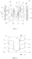
- a smart card contact pad 10 which comprises a, preferably flexible and/or imageable, circuit substrate body 12, which may be printed, printable or otherwise able to have an electronic circuit applied thereto or provided thereon, a card-reader contact element 14 on a card-reader contact side 16 of the flexible imageable circuit substrate body 12, and a chip connection element, preferably being a flip-chip connection element 18, on a chip mounting side 20 of the flexible imageable circuit substrate body 12 and which is opposite to the card-reader contact side 16.
- the flexible imageable circuit substrate body 12 is preferably a flexible plastics carrier strip 22, for example, formed from PET, and may have thickness in a range of 55 microns to 95 microns, and more preferably a thickness which is or is substantially 75 microns.
- the flexible plastics carrier strip 22 may be light transmissible, and in this example is transparent.
- the circuit substrate 12 is imageable, that is, being capable of supporting or having thereon an electrical circuit image, either on the surface of or integrated with the body of the circuit substrate 12.
- the circuit substrate 12 is preferably a printed circuit film, but any other suitable means of creating a circuit image may be utilised, as explained above.
- a non-flexible circuit substrate may be utilised.
- the card-reader contact element 14 comprises a plurality of electrically conductive overlying layers, applied preferably using electrodeposition.
- This substrate-side electrically conductive layer 24 is preferably in a range of 5 microns to 25 microns, and more preferably 10 microns or approximately 10 microns.
- the intermediate electrically conductive layer 26 is in contiguous uninterrupted contact with the substrate-side electrically conductive layer 24, and preferably has a thickness in a range of 1.0 micron to 4 microns, and more preferably 2.5 microns or approximately 2.5 microns.
- this outer electrically conductive layer 28 is in contiguous uninterrupted contact with the intermediate electrically conductive layer 26, and preferably has a thickness in the range of 0.02 microns to 0.08 microns, and more preferably 0.045 microns or approximately 0.045 microns.
- the layers of the card-reader contact element 14 are all preferably metal, and additional intermediate layers may be utilised as required.
- Contacts C1 to C8 are defined in the card-reader contact element 14, preferably by etching, and in this case a wet etching process may be conveniently utilised. Although eight contacts are provided, more or less than eight contacts may be utilised as necessity dictates.
- contacts C1 to C8 are as follows: the first contact C1, known as VCC, is utilised for power connection through which operating power is supplied to the microprocessor chip in the card; the second contact C2, known as RST, is utilised as a reset line through which an interface device can signal to a microprocessor chip of the smart card to initiate its reset sequence of instructions; the third contact C3, known as CLK, is the clock signal line through which a clock signal can be provided to the microprocessor chip, controlling the operation speed and providing a common framework for data communication between the interface device and an integrated circuit card; the fourth contact C4, known as RFU, is presently reserved for future use; the fifth contact C5, known as GND, is the ground line providing common electrical ground between the interface device and the integrated circuit card; the sixth contact C6, also known as VPP, provides a programming power connection used to program EEPROM of first generation integrated circuit cards; the seventh contact C7, also denoted as I/O, is an input/output line that provides a half-duplex communication channel between
- the flip-chip connection element 18 also comprises a plurality of electrically conductive overlying layers forming an electrically conductive trace 19 extending from an IC chip terminal or terminals 21 to a contact pad terminal or terminals 23 extending through the flexible plastics carrier strip 22 to respective contacts C1 to C8, and which again which may be conveniently applied utilising electrodeposition.
- a further substrate-side electrically conductive layer 32 in this case being or including copper, is applied to the flip-chip mounting side 20 of the substrate body 12.
- This further substrate-side electrically conductive layer 32 is again preferably in a range of 5 microns to 25 microns, and more preferably 10 microns or approximately 10 microns.
- a further outer electrically conductive layer 34 in this case being or including nickel instead of being gold or a gold composition, is then applied to overlie the further substrate-side electrically conductive layer 32, thus forming a chip terminal connection surface 36.
- This further outer electrically conductive layer 34 is in contiguous uninterrupted contact with the further substrate-side electrically conductive layer 32, and may have a thickness in a range of 1 micron to 4 microns, and more preferably 2.5 microns or approximately 2.5 microns.
- the card-reader contact surface 30 is or includes gold, due largely to its low reactivity with environmental agents and aesthetics, any suitable electrically-conductive noble metal, and preferably a precious metal such as platinum, can be considered for use.
- any suitable electrically-conductive noble metal and preferably a precious metal such as platinum, can be considered for use.
- nickel or a nickel composition is suggested for the chip terminal connection surface 36 to which the terminals of the IC chip are engaged.
- any suitable electrically-conductive non-noble metal being resistant to corrosion and oxidation may be utilised.
- the terminals of an IC chip can thus be mounted to the chip terminal connection surface 36, preferably using a conventional flip-chip mounting procedure.
- a flip-chip mounting technique or procedure is preferred, it is feasible that other mounting means may be considered and/or utilised.
- a smart card contact pad 10 which again comprises a, preferably flexible and/or imageable, circuit substrate body 12, a card-reader contact element 14 on a card-reader contact side 16 of the flexible imageable circuit substrate body 12, and a, preferably flip-chip, connection element 18 on a chip mounting side 20 of the flexible imageable circuit substrate body 12 and which is opposite to the card-reader contact side 16.
- a smart card contact pad 10 again comprises a, preferably flexible and/or imageable, circuit substrate body 12, a card-reader contact element 14 on a card-reader contact side 16 of the flexible imageable circuit substrate body 12, and a, preferably flip-chip, connection element 18 on a chip mounting side 20 of the flexible imageable circuit substrate body 12 and which is opposite to the card-reader contact side 16.
- the flip-chip connection element 18 includes the, preferably copper or copper composition, substrate-side electrically conductive layer 24.
- the, preferably nickel or nickel composition, electrically conductive layer now forms a further intermediate electrically conductive layer 126, and outer electrically conductive layer 128 is a corrosion-protection layer 138 which in this case is of an organic non-porous, preferably thiol-based, material 140 contiguously formed over a whole outwardly facing surface 142 of the further intermediate electrically conductive layer 126.
- the corrosion-protection layer 138 may form part of the chip connection element 18, or it may be considered to be separate and thus formed to overlie the chip connection element 18.
- the corrosion-protection layer 138 may be a self-assembled mono-layer 144, whereby an unbroken overlying barrier surface 146 can thus be provided.
- the corrosion-protection layer may not be electrically conductive, as necessity requires.
- the organic non-porous thiol-based material 140 is suggested due to it being electrically conductive, light transmissible, in this case preferably transparent, and anti-allergenic with human contact.
- Such a corrosion-protection layer 138 thus retains electrical conductivity with the further intermediate electrically conductive layer 126 which it overlies.
- the stoichiometry of this organometallic corrosion-protection layer 138 mitigates the formation of nickel oxides during the application of the self-assembled mono-layer 144. Creep corrosion is a known phenomenon causing premature failure of electrical components due to an increasingly sulphur-laden atmospheric environment, and the corrosion-protection layer 138 of the present invention forms a barrier against these deleterious effects.
- a suitable said corrosion-protection layer is now available from Parlex USA, Incorporated of One Parlex Place, Methuen, MA 01844, USA under product number N019292.
- a further said corrosion-protection layer 148 which overlies the gold or gold composition electrically conductive layer 28 of the card-reader contact element 14. This is advantageous in that a thickness of the gold or gold composition electrically conductive layer 28 may then be reduced whilst maintaining the outwards aesthetic appearance. Again, it is advantageous to utilise such a further corrosion-protection layer 148 to reduce the exposure of the noble metal electrically conductive layer 28 to the corrosive effects of a sulphur containing environment.
- the further corrosion-protection layer 148 is, in this case, electrically conductive and thus has the same elements as described above with reference to the first said corrosion-protection layer. However, the further corrosion-protection layer may be non-electrically conductive and/or may not necessarily be organometallic.
- a further corrosion-protection layer 148 reduces a galvanic nature of the card-reader contact element 14 due to the non-noble metals of the substrate-side and intermediate electrically conductive layers 24, 26 producing a galvanic cell with half-cell reactions.
- the smart card contact pad 10 as a plurality of smart card contact pads on the carrier strip 22 using roll-to-roll processing.
- the flexible carrier strip 22 is fed through a roll-to-roll transfer system 150, and the card-reader contact element 14 and the flip-chip connection element 18 are applied using a staged process. It may be that one of the card-reader contact element 14 and the flip-chip connection element 18 is applied first, see reference 152, with the other being applied thereafter, see reference 154. However, both the card-reader contact element 14 and the flip-chip connection element 18 may be applied simultaneously during transfer of the carrier strip 22 through the roll-to-roll transfer system 150.
- each smart card contact pad 10 can be individually mounted to a suitable carrier to form a required smart card, such as a telecommunications SIM card or bank card, for example.
- the smart card contact pad shown in Figure 7 has a first flip-chip 200, which includes a plurality of chip pads 202, each of which is attached to an electrically-conductive stud bump 204. Stud bumps 204 are preferably pointed or sharp to make point contact with the chip contact element 18 to form an electrical connection therewith.
- the flip-chip 200 is preferably fixed to the contact pad by an adhesive 160.
- the adhesive is in the form of a paste or film.
- the adhesive is preferably not electrically conductive for cost reasons. However, anisotropic (z-axis) conductive adhesive may be used even though it is more expensive. The adhesive holds the bumps in contact with the chip contact element.
- the smart card contact pad shown in Figure 8 could be utilised, referenced globally as 101.
- Attached is a second flip-chip 300, which also includes a plurality of chip pads 302, each of which is attached to an electrically-conductive plated bump or projection 304, in this case being slim line and having a lower profile than the stud bump 204 above.
- the plated bump 304 abuts or sits on the outer electrically conductive layer 128 of the chip contact element 18, thereby making a surface or area contact with the outermost layer, to electrically connect the chip to the chip contact element 18.
- the flip-chip 300 is preferably adhered using an adhesive 160 to hold the plated bumps 304 in contact with the chip contact element.
- the card-reader contact side 16 preferably comprises four layers on top of the flexible imageable circuit substrate body 12, namely the substrate-side electrically conductive layer 24, the non-noble metal intermediate electrically conductive layer 26, the noble metal outer electrically conductive layer 28 and the further corrosion-protection layer 148.
- the further corrosion-protection layer 148 it may be possible, in an example useful for understanding the invention, to efficiently electrically connect the flip-chip 300 to the card-reader contact element 14 without necessarily providing the non-noble metal intermediate electrically conductive layer 26. Removal of the non-noble metal intermediate electrically conductive layer 26 will accordingly reduce the expenditure of the smart card contact pad 10.
- the mounting adhesive 160 could be used as a barrier to oxidation or corrosion of the further intermediate electrically conductive layer 126 in place of the corrosion protection layer 138, reducing the number of components required to form the smart card contact pad 10. If the mounting adhesive 160 is used for this purpose, the noble metal outer electrically conductive layer 28 may still require the separate further corrosion-protection layer 148. It is feasible that an adhesive or bonding agent used to apply the IC chip to the chip connection element may also be a suitable corrosion protection layer, providing it meets the requirements previously mentioned.
- a smart card contact pad having a reduced noble metal requirement. Furthermore, a utilised noble metal is only on a card-reader contact surface. It is also possible to provide a smart card contact pad having a non-noble metal chip terminal connection surface which is not or substantially not subject to corrosion or oxidation prior to the mounting of an IC chip.
Landscapes
- Engineering & Computer Science (AREA)
- Physics & Mathematics (AREA)
- General Physics & Mathematics (AREA)
- Theoretical Computer Science (AREA)
- Computer Hardware Design (AREA)
- Microelectronics & Electronic Packaging (AREA)
- Credit Cards Or The Like (AREA)
- Preventing Corrosion Or Incrustation Of Metals (AREA)
Claims (15)
- Kontaktbehaftete Smartcard, umfassend ein Smartcard-Kontaktpad (10; 100; 101) und einen Flip-Chip-montierten IC-Chip (200; 300), wobei das Smartcard-Kontaktpad (10; 100; 101) einen von Rolle zu Rolle übertragbaren flexiblen Trägerstreifen (22), ein Kartenleser-Kontaktelement (14) auf einer ersten Seite (16) des von Rolle zu Rolle übertragbaren flexiblen Trägerstreifens (22) und ein Chipverbindungselement (18) auf einer zweiten Seite (20) des von Rolle zu Rolle übertragbaren flexiblen Trägerstreifens (22), die der ersten Seite (16) gegenüberliegt, enthält, wobei das Kartenleser-Kontaktelement (14) eine elektrisch leitende Edelmetallfläche (30) aufweist, wobei das Chipverbindungselement (18) eine Chipanschluss-Verbindungsfläche (142) aufweist, die eine Außenfläche einer ersten elektrisch leitenden Schicht (126) ist und die erste elektrisch leitende Schicht aus Nicht-Edelmetall besteht, und wobei der Flip-Chip-montierte IC-Chip (200; 300), der an der zweiten Seite (20) des von Rolle zu Rolle übertragbaren flexiblen Trägerstreifens (22) flip-chip-gemäß montiert und elektrisch mit der Chipanschluss-Verbindungsfläche (142) verbunden ist, und gekennzeichnet durch eine elektrisch leitende Korrosionsschutzschicht (138), die die erste elektrisch leitende Schicht (126) auf der Außenfläche überlagert.
- Kontaktbehaftete Smartcard nach Anspruch 1, wobei das Edelmetall Gold ist oder enthält.
- Kontaktbehaftete Smartcard nach Anspruch 1 oder Anspruch 2, weiter umfassend eine zweite elektrisch leitende Schicht (24) auf der ersten Seite (16) des von Rolle zu Rolle übertragbaren flexiblen Trägerstreifens (22), die eine Dicke in einem Bereich von 5 Mikron bis 25 Mikron aufweist.
- Kontaktbehaftete Smartcard nach Anspruch 3, weiter umfassend eine elektrisch leitende Zwischenschicht (26), die die zweite elektrisch leitende Schicht (24) überlagert und eine Dicke von 1 Mikron bis 4 Mikron aufweist.
- Kontaktbehaftete Smartcard nach Anspruch 4, wobei die elektrisch leitende Edelmetallfläche (30) eine Außenfläche einer elektrisch leitenden Edelmetallschicht (28) ist, die die elektrisch leitende Zwischenschicht (26) überlagert.
- Kontaktbehaftete Smartcard nach Anspruch 5, wobei die elektrisch leitende Edelmetallschicht (28) eine Dicke im Bereich von 0,02 Mikrometer bis 0,08 Mikrometer aufweist.
- Kontaktbehaftete Smartcard nach einem der Ansprüche 4 bis 6, wobei mindestens eine zusätzliche Zwischenschicht bereitgestellt ist.
- Kontaktbehaftete Smartcard nach einem der vorstehenden Ansprüche, wobei der von Rolle zu Rolle übertragbare flexible Trägerstreifen (22) aus PET gebildet ist und eine Dicke in einem Bereich von 55 Mikron bis 95 Mikron aufweist.
- Kontaktbehaftete Smartcard nach einem der vorstehenden Ansprüche, weiter umfassend eine substratseitige elektrisch leitende Schicht (32) auf der zweiten Seite (20) des von Rolle zu Rolle übertragbaren flexiblen Trägerstreifens (22), wobei die elektrisch leitende Schicht (126) die substratseitige elektrisch leitende Schicht (32) überlagert.
- Kontaktbehaftete Smartcard nach einem der vorstehenden Ansprüche, weiter umfassend eine zusätzliche elektrisch leitende Korrosionsschutzschicht (148), die die elektrisch leitende Edelmetallfläche (30) überlagert.
- SIM-Karte, die ein Trägersubstrat und eine kontaktbehaftete Smartcard nach einem der vorstehenden Ansprüche umfasst, und die durch das Trägersubstrat getragen wird
- Bankkarte, die ein Trägersubstrat und eine kontaktbehaftete Smartcard nach einem der Ansprüche 1 bis 10 umfasst, und die durch das Trägersubstrat getragen wird.
- Verfahren zur Herstellung eines Smartcard-Kontaktpads (10; 100; 101), wobei das Verfahren die Schritte umfasst von: a] Zuführen eines von Rolle zu Rolle übertragbaren flexiblen Trägerstreifens (22) durch ein Rolle-zu-Rolle-Übertragungssystem (150); b] Aufbringen eines Kartenleser-Kontaktelements (14) auf eine erste Seite (16) des von Rolle zu Rolle übertragbaren flexiblen Trägerstreifens (22); c] Aufbringen eines Flip-Chip-Verbindungselements (18) auf eine zweite Seite (20) des von Rolle zu Roll - übertragbaren flexiblen Trägerstreifens (22), die der ersten Seite (16) gegenüberliegt, wobei das Kartenleser-Kontaktelement (14) eine elektrisch leitende Edelmetallfläche (30) aufweist und das Chipverbindungselement (18) eine Chip-Anschlussverbindungsfläche (142) aufweist, die eine Außenfläche einer elektrisch leitenden Schicht (126) ist und aus Nicht-Edelmetall besteht, wodurch ein Smartcard-Kontaktpad (10; 100; 101) auf dem von Rolle zu Rolle übertragbaren flexiblen Trägerstreifen (22) gebildet wird; dadurch gekennzeichnet, dass eine elektrisch leitende Korrosionsschutzschicht (138) vorhanden ist, die die Außenfläche über der elektrisch leitenden Schicht (126) überlagert; und d] Entfernen des Kontaktbehaftete Smartcards (10; 100; 101) von dem von Rolle zu Rolle übertragbaren flexiblen Trägerstreifen (22).
- Verfahren nach Anspruch 13, wobei die Schritte b] und c] unter Verwendung eines in mehreren Schritten ablaufenden Prozesses angewendet werden.
- Verfahren nach Anspruch 13 oder Anspruch 14, weiter umfassend den Schritt des Montierens des Smartcard-Kontaktpads (10; 100; 101) an einem Träger, um eine Smartcard zu bilden.
Applications Claiming Priority (2)
| Application Number | Priority Date | Filing Date | Title |
|---|---|---|---|
| CN201310125487 | 2013-04-11 | ||
| EP14164108.4A EP2790131B1 (de) | 2013-04-11 | 2014-04-09 | Kontakt für Chipkarte mit Oxidationsschutz |
Related Parent Applications (2)
| Application Number | Title | Priority Date | Filing Date |
|---|---|---|---|
| EP14164108.4A Division-Into EP2790131B1 (de) | 2013-04-11 | 2014-04-09 | Kontakt für Chipkarte mit Oxidationsschutz |
| EP14164108.4A Division EP2790131B1 (de) | 2013-04-11 | 2014-04-09 | Kontakt für Chipkarte mit Oxidationsschutz |
Publications (2)
| Publication Number | Publication Date |
|---|---|
| EP3270328A1 EP3270328A1 (de) | 2018-01-17 |
| EP3270328B1 true EP3270328B1 (de) | 2021-05-26 |
Family
ID=50732776
Family Applications (2)
| Application Number | Title | Priority Date | Filing Date |
|---|---|---|---|
| EP17182828.8A Active EP3270328B1 (de) | 2013-04-11 | 2014-04-09 | Verbesserungen an oder im zusammenhang mit kontaktchipkarten |
| EP14164108.4A Active EP2790131B1 (de) | 2013-04-11 | 2014-04-09 | Kontakt für Chipkarte mit Oxidationsschutz |
Family Applications After (1)
| Application Number | Title | Priority Date | Filing Date |
|---|---|---|---|
| EP14164108.4A Active EP2790131B1 (de) | 2013-04-11 | 2014-04-09 | Kontakt für Chipkarte mit Oxidationsschutz |
Country Status (6)
| Country | Link |
|---|---|
| US (2) | US9251457B2 (de) |
| EP (2) | EP3270328B1 (de) |
| JP (1) | JP6416491B2 (de) |
| CN (2) | CN104102941B (de) |
| BR (1) | BR102014008914B1 (de) |
| TW (1) | TWI633492B (de) |
Families Citing this family (6)
| Publication number | Priority date | Publication date | Assignee | Title |
|---|---|---|---|---|
| GB201510252D0 (en) * | 2015-06-12 | 2015-07-29 | Johnson Electric Sa | Coloured smart card module and smart card |
| CN107025481B (zh) * | 2016-02-02 | 2021-08-20 | 上海伯乐电子有限公司 | 柔性印制电路板及应用其的智能卡模块和智能卡 |
| CN107679611A (zh) * | 2017-10-13 | 2018-02-09 | 四川精工伟达智能技术股份有限公司 | 一种智能卡 |
| WO2021110872A1 (en) * | 2019-12-03 | 2021-06-10 | Linxens Holding | Tape for electrical circuits with rose-gold contact pads and method for manufacturing such a tape |
| US11380630B2 (en) | 2020-05-11 | 2022-07-05 | International Business Machines Corporation | Integrated circuit package that measures amount of internal precious material |
| KR20230095672A (ko) * | 2021-12-22 | 2023-06-29 | 엘지이노텍 주식회사 | 스마트 ic 기판, 스마트 ic 모듈 및 이를 포함하는 ic 카드 |
Family Cites Families (20)
| Publication number | Priority date | Publication date | Assignee | Title |
|---|---|---|---|---|
| JPS61123990A (ja) * | 1984-11-05 | 1986-06-11 | Casio Comput Co Ltd | Icカ−ド |
| FR2584235B1 (fr) * | 1985-06-26 | 1988-04-22 | Bull Sa | Procede de montage d'un circuit integre sur un support, dispositif en resultant et son application a une carte a microcircuits electroniques |
| JPS6259096A (ja) * | 1985-09-10 | 1987-03-14 | カシオ計算機株式会社 | Icカ−ド |
| JPH0569691A (ja) * | 1991-09-17 | 1993-03-23 | Fujitsu General Ltd | Icカード |
| DE19632113C1 (de) * | 1996-08-08 | 1998-02-19 | Siemens Ag | Chipkarte, Verfahren zur Herstellung einer Chipkarte und Halbleiterchip zur Verwendung in einer Chipkarte |
| US6404643B1 (en) * | 1998-10-15 | 2002-06-11 | Amerasia International Technology, Inc. | Article having an embedded electronic device, and method of making same |
| US6288905B1 (en) * | 1999-04-15 | 2001-09-11 | Amerasia International Technology Inc. | Contact module, as for a smart card, and method for making same |
| DE10016715C1 (de) * | 2000-04-04 | 2001-09-06 | Infineon Technologies Ag | Herstellungsverfahren für laminierte Chipkarten |
| DE10139395A1 (de) * | 2001-08-10 | 2003-03-06 | Infineon Technologies Ag | Kontaktierung von Halbleiterchips in Chipkarten |
| US6433359B1 (en) * | 2001-09-06 | 2002-08-13 | 3M Innovative Properties Company | Surface modifying layers for organic thin film transistors |
| KR100723491B1 (ko) * | 2005-07-14 | 2007-05-30 | 삼성전자주식회사 | 범용 인쇄 회로 기판 및 이를 사용한 스마트 카드 |
| EP1785916B1 (de) * | 2005-11-14 | 2009-08-19 | Tyco Electronics France SAS | Smartcard-Körper, Smartcard und Herstellungsverfahren |
| DE102006060719A1 (de) * | 2006-12-21 | 2008-06-26 | Infineon Technologies Ag | Chipkartenmodul und Verfahren zur Herstellung eines Chipkartenmoduls |
| EP2228754A1 (de) * | 2007-12-10 | 2010-09-15 | Renesas Electronics Corporation | Sim-adapter und sim-karte |
| US8249655B2 (en) * | 2008-12-18 | 2012-08-21 | At&T Intellectual Property I, L.P. | Universal serial bus based subscriber identity module |
| CN101770600A (zh) * | 2009-12-31 | 2010-07-07 | 北京握奇数据系统有限公司 | 一种非接触式智能卡及其制作方法 |
| CN102117929A (zh) * | 2010-01-05 | 2011-07-06 | 三星Sdi株式会社 | 二次电池和智能卡 |
| US20120328904A1 (en) * | 2011-06-23 | 2012-12-27 | Xtalic Corporation | Printed circuit boards and related articles including electrodeposited coatings |
| CN102395247A (zh) | 2011-10-10 | 2012-03-28 | 青岛琴岛控制器有限公司 | 单面镀金的pcb线路板 |
| CN102360447A (zh) * | 2011-11-01 | 2012-02-22 | 上海祯显电子科技有限公司 | 一种薄膜基板 |
-
2014
- 2014-04-08 CN CN201410138183.3A patent/CN104102941B/zh active Active
- 2014-04-08 CN CN201420167064.6U patent/CN203894790U/zh not_active Expired - Lifetime
- 2014-04-09 EP EP17182828.8A patent/EP3270328B1/de active Active
- 2014-04-09 EP EP14164108.4A patent/EP2790131B1/de active Active
- 2014-04-10 US US14/249,722 patent/US9251457B2/en active Active
- 2014-04-11 BR BR102014008914-4A patent/BR102014008914B1/pt active IP Right Grant
- 2014-04-11 TW TW103113387A patent/TWI633492B/zh active
- 2014-04-11 JP JP2014081778A patent/JP6416491B2/ja active Active
-
2015
- 2015-12-18 US US14/975,187 patent/US9524459B2/en active Active
Non-Patent Citations (1)
| Title |
|---|
| None * |
Also Published As
| Publication number | Publication date |
|---|---|
| JP2014206978A (ja) | 2014-10-30 |
| JP6416491B2 (ja) | 2018-10-31 |
| EP2790131B1 (de) | 2017-09-20 |
| EP2790131A1 (de) | 2014-10-15 |
| US9524459B2 (en) | 2016-12-20 |
| CN203894790U (zh) | 2014-10-22 |
| US9251457B2 (en) | 2016-02-02 |
| TWI633492B (zh) | 2018-08-21 |
| US20160104063A1 (en) | 2016-04-14 |
| TW201443788A (zh) | 2014-11-16 |
| US20140306016A1 (en) | 2014-10-16 |
| EP3270328A1 (de) | 2018-01-17 |
| CN104102941A (zh) | 2014-10-15 |
| BR102014008914B1 (pt) | 2022-02-01 |
| CN104102941B (zh) | 2023-10-13 |
| BR102014008914A2 (pt) | 2014-12-23 |
Similar Documents
| Publication | Publication Date | Title |
|---|---|---|
| US10810477B2 (en) | Method for producing a circuit for a chip card module and circuit for a chip card module | |
| US9524459B2 (en) | Contact smart card | |
| US6853087B2 (en) | Component and antennae assembly in radio frequency identification devices | |
| CN109583552B (zh) | 用于制造便携式数据载体的方法及数据载体主体 | |
| CN1555577A (zh) | 形成于其上形成多数载体组件条带或面板之不导电基板 | |
| US20110189824A1 (en) | Method for manufacturing an electronic device | |
| JP4952266B2 (ja) | デュアルインターフェースicカードとその製造方法、接触・非接触兼用icモジュール | |
| EP3062266B1 (de) | Ic-modul, ic-karte und ic-modulsubstrat | |
| JPWO2007058108A1 (ja) | 異方導電接着剤 | |
| CN203490719U (zh) | 智能卡及智能卡触板 | |
| HK40051873A (en) | Method for producing a circuit for a chip card module and circuit for a chip card module | |
| HK40051873B (en) | Method for producing a circuit for a chip card module and circuit for a chip card module | |
| HK1234185A1 (en) | Method for producing a circuit for a chip card module and circuit for a chip card module | |
| JP2001053395A (ja) | 電子回路基板 | |
| HK1234185B (en) | Method for producing a circuit for a chip card module and circuit for a chip card module |
Legal Events
| Date | Code | Title | Description |
|---|---|---|---|
| PUAI | Public reference made under article 153(3) epc to a published international application that has entered the european phase |
Free format text: ORIGINAL CODE: 0009012 |
|
| STAA | Information on the status of an ep patent application or granted ep patent |
Free format text: STATUS: THE APPLICATION HAS BEEN PUBLISHED |
|
| AC | Divisional application: reference to earlier application |
Ref document number: 2790131 Country of ref document: EP Kind code of ref document: P |
|
| AK | Designated contracting states |
Kind code of ref document: A1 Designated state(s): AL AT BE BG CH CY CZ DE DK EE ES FI FR GB GR HR HU IE IS IT LI LT LU LV MC MK MT NL NO PL PT RO RS SE SI SK SM TR |
|
| STAA | Information on the status of an ep patent application or granted ep patent |
Free format text: STATUS: REQUEST FOR EXAMINATION WAS MADE |
|
| 17P | Request for examination filed |
Effective date: 20180717 |
|
| RBV | Designated contracting states (corrected) |
Designated state(s): AL AT BE BG CH CY CZ DE DK EE ES FI FR GB GR HR HU IE IS IT LI LT LU LV MC MK MT NL NO PL PT RO RS SE SI SK SM TR |
|
| STAA | Information on the status of an ep patent application or granted ep patent |
Free format text: STATUS: EXAMINATION IS IN PROGRESS |
|
| 17Q | First examination report despatched |
Effective date: 20181203 |
|
| RAP1 | Party data changed (applicant data changed or rights of an application transferred) |
Owner name: JOHNSON ELECTRIC INTERNATIONAL AG |
|
| GRAP | Despatch of communication of intention to grant a patent |
Free format text: ORIGINAL CODE: EPIDOSNIGR1 |
|
| STAA | Information on the status of an ep patent application or granted ep patent |
Free format text: STATUS: GRANT OF PATENT IS INTENDED |
|
| INTG | Intention to grant announced |
Effective date: 20201214 |
|
| GRAS | Grant fee paid |
Free format text: ORIGINAL CODE: EPIDOSNIGR3 |
|
| GRAA | (expected) grant |
Free format text: ORIGINAL CODE: 0009210 |
|
| STAA | Information on the status of an ep patent application or granted ep patent |
Free format text: STATUS: THE PATENT HAS BEEN GRANTED |
|
| AC | Divisional application: reference to earlier application |
Ref document number: 2790131 Country of ref document: EP Kind code of ref document: P |
|
| AK | Designated contracting states |
Kind code of ref document: B1 Designated state(s): AL AT BE BG CH CY CZ DE DK EE ES FI FR GB GR HR HU IE IS IT LI LT LU LV MC MK MT NL NO PL PT RO RS SE SI SK SM TR |
|
| REG | Reference to a national code |
Ref country code: GB Ref legal event code: FG4D |
|
| REG | Reference to a national code |
Ref country code: CH Ref legal event code: EP |
|
| REG | Reference to a national code |
Ref country code: AT Ref legal event code: REF Ref document number: 1396960 Country of ref document: AT Kind code of ref document: T Effective date: 20210615 |
|
| REG | Reference to a national code |
Ref country code: DE Ref legal event code: R096 Ref document number: 602014077824 Country of ref document: DE |
|
| REG | Reference to a national code |
Ref country code: IE Ref legal event code: FG4D |
|
| REG | Reference to a national code |
Ref country code: LT Ref legal event code: MG9D |
|
| REG | Reference to a national code |
Ref country code: AT Ref legal event code: MK05 Ref document number: 1396960 Country of ref document: AT Kind code of ref document: T Effective date: 20210526 |
|
| PG25 | Lapsed in a contracting state [announced via postgrant information from national office to epo] |
Ref country code: BG Free format text: LAPSE BECAUSE OF FAILURE TO SUBMIT A TRANSLATION OF THE DESCRIPTION OR TO PAY THE FEE WITHIN THE PRESCRIBED TIME-LIMIT Effective date: 20210826 Ref country code: AT Free format text: LAPSE BECAUSE OF FAILURE TO SUBMIT A TRANSLATION OF THE DESCRIPTION OR TO PAY THE FEE WITHIN THE PRESCRIBED TIME-LIMIT Effective date: 20210526 Ref country code: HR Free format text: LAPSE BECAUSE OF FAILURE TO SUBMIT A TRANSLATION OF THE DESCRIPTION OR TO PAY THE FEE WITHIN THE PRESCRIBED TIME-LIMIT Effective date: 20210526 Ref country code: FI Free format text: LAPSE BECAUSE OF FAILURE TO SUBMIT A TRANSLATION OF THE DESCRIPTION OR TO PAY THE FEE WITHIN THE PRESCRIBED TIME-LIMIT Effective date: 20210526 Ref country code: LT Free format text: LAPSE BECAUSE OF FAILURE TO SUBMIT A TRANSLATION OF THE DESCRIPTION OR TO PAY THE FEE WITHIN THE PRESCRIBED TIME-LIMIT Effective date: 20210526 |
|
| REG | Reference to a national code |
Ref country code: NL Ref legal event code: MP Effective date: 20210526 |
|
| PG25 | Lapsed in a contracting state [announced via postgrant information from national office to epo] |
Ref country code: PL Free format text: LAPSE BECAUSE OF FAILURE TO SUBMIT A TRANSLATION OF THE DESCRIPTION OR TO PAY THE FEE WITHIN THE PRESCRIBED TIME-LIMIT Effective date: 20210526 Ref country code: NO Free format text: LAPSE BECAUSE OF FAILURE TO SUBMIT A TRANSLATION OF THE DESCRIPTION OR TO PAY THE FEE WITHIN THE PRESCRIBED TIME-LIMIT Effective date: 20210826 Ref country code: PT Free format text: LAPSE BECAUSE OF FAILURE TO SUBMIT A TRANSLATION OF THE DESCRIPTION OR TO PAY THE FEE WITHIN THE PRESCRIBED TIME-LIMIT Effective date: 20210927 Ref country code: SE Free format text: LAPSE BECAUSE OF FAILURE TO SUBMIT A TRANSLATION OF THE DESCRIPTION OR TO PAY THE FEE WITHIN THE PRESCRIBED TIME-LIMIT Effective date: 20210526 Ref country code: RS Free format text: LAPSE BECAUSE OF FAILURE TO SUBMIT A TRANSLATION OF THE DESCRIPTION OR TO PAY THE FEE WITHIN THE PRESCRIBED TIME-LIMIT Effective date: 20210526 Ref country code: IS Free format text: LAPSE BECAUSE OF FAILURE TO SUBMIT A TRANSLATION OF THE DESCRIPTION OR TO PAY THE FEE WITHIN THE PRESCRIBED TIME-LIMIT Effective date: 20210926 Ref country code: GR Free format text: LAPSE BECAUSE OF FAILURE TO SUBMIT A TRANSLATION OF THE DESCRIPTION OR TO PAY THE FEE WITHIN THE PRESCRIBED TIME-LIMIT Effective date: 20210827 Ref country code: LV Free format text: LAPSE BECAUSE OF FAILURE TO SUBMIT A TRANSLATION OF THE DESCRIPTION OR TO PAY THE FEE WITHIN THE PRESCRIBED TIME-LIMIT Effective date: 20210526 |
|
| PG25 | Lapsed in a contracting state [announced via postgrant information from national office to epo] |
Ref country code: NL Free format text: LAPSE BECAUSE OF FAILURE TO SUBMIT A TRANSLATION OF THE DESCRIPTION OR TO PAY THE FEE WITHIN THE PRESCRIBED TIME-LIMIT Effective date: 20210526 |
|
| PG25 | Lapsed in a contracting state [announced via postgrant information from national office to epo] |
Ref country code: SM Free format text: LAPSE BECAUSE OF FAILURE TO SUBMIT A TRANSLATION OF THE DESCRIPTION OR TO PAY THE FEE WITHIN THE PRESCRIBED TIME-LIMIT Effective date: 20210526 Ref country code: SK Free format text: LAPSE BECAUSE OF FAILURE TO SUBMIT A TRANSLATION OF THE DESCRIPTION OR TO PAY THE FEE WITHIN THE PRESCRIBED TIME-LIMIT Effective date: 20210526 Ref country code: CZ Free format text: LAPSE BECAUSE OF FAILURE TO SUBMIT A TRANSLATION OF THE DESCRIPTION OR TO PAY THE FEE WITHIN THE PRESCRIBED TIME-LIMIT Effective date: 20210526 Ref country code: DK Free format text: LAPSE BECAUSE OF FAILURE TO SUBMIT A TRANSLATION OF THE DESCRIPTION OR TO PAY THE FEE WITHIN THE PRESCRIBED TIME-LIMIT Effective date: 20210526 Ref country code: EE Free format text: LAPSE BECAUSE OF FAILURE TO SUBMIT A TRANSLATION OF THE DESCRIPTION OR TO PAY THE FEE WITHIN THE PRESCRIBED TIME-LIMIT Effective date: 20210526 Ref country code: RO Free format text: LAPSE BECAUSE OF FAILURE TO SUBMIT A TRANSLATION OF THE DESCRIPTION OR TO PAY THE FEE WITHIN THE PRESCRIBED TIME-LIMIT Effective date: 20210526 Ref country code: ES Free format text: LAPSE BECAUSE OF FAILURE TO SUBMIT A TRANSLATION OF THE DESCRIPTION OR TO PAY THE FEE WITHIN THE PRESCRIBED TIME-LIMIT Effective date: 20210526 |
|
| REG | Reference to a national code |
Ref country code: DE Ref legal event code: R097 Ref document number: 602014077824 Country of ref document: DE |
|
| PLBE | No opposition filed within time limit |
Free format text: ORIGINAL CODE: 0009261 |
|
| STAA | Information on the status of an ep patent application or granted ep patent |
Free format text: STATUS: NO OPPOSITION FILED WITHIN TIME LIMIT |
|
| 26N | No opposition filed |
Effective date: 20220301 |
|
| PG25 | Lapsed in a contracting state [announced via postgrant information from national office to epo] |
Ref country code: IS Free format text: LAPSE BECAUSE OF FAILURE TO SUBMIT A TRANSLATION OF THE DESCRIPTION OR TO PAY THE FEE WITHIN THE PRESCRIBED TIME-LIMIT Effective date: 20210926 Ref country code: AL Free format text: LAPSE BECAUSE OF FAILURE TO SUBMIT A TRANSLATION OF THE DESCRIPTION OR TO PAY THE FEE WITHIN THE PRESCRIBED TIME-LIMIT Effective date: 20210526 |
|
| PG25 | Lapsed in a contracting state [announced via postgrant information from national office to epo] |
Ref country code: IT Free format text: LAPSE BECAUSE OF FAILURE TO SUBMIT A TRANSLATION OF THE DESCRIPTION OR TO PAY THE FEE WITHIN THE PRESCRIBED TIME-LIMIT Effective date: 20210526 |
|
| REG | Reference to a national code |
Ref country code: DE Ref legal event code: R081 Ref document number: 602014077824 Country of ref document: DE Owner name: PARLEX PACIFIC LIMITED, HONG KONG, CN Free format text: FORMER OWNER: JOHNSON ELECTRIC INTERNATIONAL AG, MURTEN, CH |
|
| REG | Reference to a national code |
Ref country code: CH Ref legal event code: PL |
|
| GBPC | Gb: european patent ceased through non-payment of renewal fee |
Effective date: 20220409 |
|
| REG | Reference to a national code |
Ref country code: BE Ref legal event code: MM Effective date: 20220430 |
|
| PG25 | Lapsed in a contracting state [announced via postgrant information from national office to epo] |
Ref country code: MC Free format text: LAPSE BECAUSE OF FAILURE TO SUBMIT A TRANSLATION OF THE DESCRIPTION OR TO PAY THE FEE WITHIN THE PRESCRIBED TIME-LIMIT Effective date: 20210526 Ref country code: LU Free format text: LAPSE BECAUSE OF NON-PAYMENT OF DUE FEES Effective date: 20220409 Ref country code: LI Free format text: LAPSE BECAUSE OF NON-PAYMENT OF DUE FEES Effective date: 20220430 Ref country code: GB Free format text: LAPSE BECAUSE OF NON-PAYMENT OF DUE FEES Effective date: 20220409 Ref country code: FR Free format text: LAPSE BECAUSE OF NON-PAYMENT OF DUE FEES Effective date: 20220430 Ref country code: CH Free format text: LAPSE BECAUSE OF NON-PAYMENT OF DUE FEES Effective date: 20220430 |
|
| PG25 | Lapsed in a contracting state [announced via postgrant information from national office to epo] |
Ref country code: BE Free format text: LAPSE BECAUSE OF NON-PAYMENT OF DUE FEES Effective date: 20220430 |
|
| PG25 | Lapsed in a contracting state [announced via postgrant information from national office to epo] |
Ref country code: IE Free format text: LAPSE BECAUSE OF NON-PAYMENT OF DUE FEES Effective date: 20220409 |
|
| REG | Reference to a national code |
Ref country code: DE Ref legal event code: R084 Ref document number: 602014077824 Country of ref document: DE |
|
| P01 | Opt-out of the competence of the unified patent court (upc) registered |
Effective date: 20230719 |
|
| PG25 | Lapsed in a contracting state [announced via postgrant information from national office to epo] |
Ref country code: HU Free format text: LAPSE BECAUSE OF FAILURE TO SUBMIT A TRANSLATION OF THE DESCRIPTION OR TO PAY THE FEE WITHIN THE PRESCRIBED TIME-LIMIT; INVALID AB INITIO Effective date: 20140409 |
|
| PG25 | Lapsed in a contracting state [announced via postgrant information from national office to epo] |
Ref country code: MK Free format text: LAPSE BECAUSE OF FAILURE TO SUBMIT A TRANSLATION OF THE DESCRIPTION OR TO PAY THE FEE WITHIN THE PRESCRIBED TIME-LIMIT Effective date: 20210526 Ref country code: CY Free format text: LAPSE BECAUSE OF FAILURE TO SUBMIT A TRANSLATION OF THE DESCRIPTION OR TO PAY THE FEE WITHIN THE PRESCRIBED TIME-LIMIT Effective date: 20210526 |
|
| PG25 | Lapsed in a contracting state [announced via postgrant information from national office to epo] |
Ref country code: TR Free format text: LAPSE BECAUSE OF FAILURE TO SUBMIT A TRANSLATION OF THE DESCRIPTION OR TO PAY THE FEE WITHIN THE PRESCRIBED TIME-LIMIT Effective date: 20210526 |
|
| PG25 | Lapsed in a contracting state [announced via postgrant information from national office to epo] |
Ref country code: MT Free format text: LAPSE BECAUSE OF FAILURE TO SUBMIT A TRANSLATION OF THE DESCRIPTION OR TO PAY THE FEE WITHIN THE PRESCRIBED TIME-LIMIT Effective date: 20210526 |
|
| PGFP | Annual fee paid to national office [announced via postgrant information from national office to epo] |
Ref country code: DE Payment date: 20250428 Year of fee payment: 12 |