EP3270218A2 - Hochauflösende anzeigevorrichtung - Google Patents
Hochauflösende anzeigevorrichtung Download PDFInfo
- Publication number
- EP3270218A2 EP3270218A2 EP17181099.7A EP17181099A EP3270218A2 EP 3270218 A2 EP3270218 A2 EP 3270218A2 EP 17181099 A EP17181099 A EP 17181099A EP 3270218 A2 EP3270218 A2 EP 3270218A2
- Authority
- EP
- European Patent Office
- Prior art keywords
- pad
- sub
- terminals
- terminal
- display device
- Prior art date
- Legal status (The legal status is an assumption and is not a legal conclusion. Google has not performed a legal analysis and makes no representation as to the accuracy of the status listed.)
- Granted
Links
Images










Classifications
-
- H—ELECTRICITY
- H10—SEMICONDUCTOR DEVICES; ELECTRIC SOLID-STATE DEVICES NOT OTHERWISE PROVIDED FOR
- H10K—ORGANIC ELECTRIC SOLID-STATE DEVICES
- H10K59/00—Integrated devices, or assemblies of multiple devices, comprising at least one organic light-emitting element covered by group H10K50/00
- H10K59/10—OLED displays
- H10K59/12—Active-matrix OLED [AMOLED] displays
- H10K59/131—Interconnections, e.g. wiring lines or terminals
-
- G—PHYSICS
- G02—OPTICS
- G02F—OPTICAL DEVICES OR ARRANGEMENTS FOR THE CONTROL OF LIGHT BY MODIFICATION OF THE OPTICAL PROPERTIES OF THE MEDIA OF THE ELEMENTS INVOLVED THEREIN; NON-LINEAR OPTICS; FREQUENCY-CHANGING OF LIGHT; OPTICAL LOGIC ELEMENTS; OPTICAL ANALOGUE/DIGITAL CONVERTERS
- G02F1/00—Devices or arrangements for the control of the intensity, colour, phase, polarisation or direction of light arriving from an independent light source, e.g. switching, gating or modulating; Non-linear optics
- G02F1/01—Devices or arrangements for the control of the intensity, colour, phase, polarisation or direction of light arriving from an independent light source, e.g. switching, gating or modulating; Non-linear optics for the control of the intensity, phase, polarisation or colour
- G02F1/13—Devices or arrangements for the control of the intensity, colour, phase, polarisation or direction of light arriving from an independent light source, e.g. switching, gating or modulating; Non-linear optics for the control of the intensity, phase, polarisation or colour based on liquid crystals, e.g. single liquid crystal display cells
- G02F1/133—Constructional arrangements; Operation of liquid crystal cells; Circuit arrangements
- G02F1/1333—Constructional arrangements; Manufacturing methods
- G02F1/1345—Conductors connecting electrodes to cell terminals
- G02F1/13452—Conductors connecting driver circuitry and terminals of panels
-
- H—ELECTRICITY
- H05—ELECTRIC TECHNIQUES NOT OTHERWISE PROVIDED FOR
- H05K—PRINTED CIRCUITS; CASINGS OR CONSTRUCTIONAL DETAILS OF ELECTRIC APPARATUS; MANUFACTURE OF ASSEMBLAGES OF ELECTRICAL COMPONENTS
- H05K1/00—Printed circuits
- H05K1/02—Details
- H05K1/11—Printed elements for providing electric connections to or between printed circuits
- H05K1/111—Pads for surface mounting, e.g. lay-out
-
- G—PHYSICS
- G02—OPTICS
- G02F—OPTICAL DEVICES OR ARRANGEMENTS FOR THE CONTROL OF LIGHT BY MODIFICATION OF THE OPTICAL PROPERTIES OF THE MEDIA OF THE ELEMENTS INVOLVED THEREIN; NON-LINEAR OPTICS; FREQUENCY-CHANGING OF LIGHT; OPTICAL LOGIC ELEMENTS; OPTICAL ANALOGUE/DIGITAL CONVERTERS
- G02F1/00—Devices or arrangements for the control of the intensity, colour, phase, polarisation or direction of light arriving from an independent light source, e.g. switching, gating or modulating; Non-linear optics
- G02F1/01—Devices or arrangements for the control of the intensity, colour, phase, polarisation or direction of light arriving from an independent light source, e.g. switching, gating or modulating; Non-linear optics for the control of the intensity, phase, polarisation or colour
- G02F1/13—Devices or arrangements for the control of the intensity, colour, phase, polarisation or direction of light arriving from an independent light source, e.g. switching, gating or modulating; Non-linear optics for the control of the intensity, phase, polarisation or colour based on liquid crystals, e.g. single liquid crystal display cells
- G02F1/133—Constructional arrangements; Operation of liquid crystal cells; Circuit arrangements
- G02F1/1333—Constructional arrangements; Manufacturing methods
- G02F1/1345—Conductors connecting electrodes to cell terminals
- G02F1/13458—Terminal pads
-
- G—PHYSICS
- G09—EDUCATION; CRYPTOGRAPHY; DISPLAY; ADVERTISING; SEALS
- G09G—ARRANGEMENTS OR CIRCUITS FOR CONTROL OF INDICATING DEVICES USING STATIC MEANS TO PRESENT VARIABLE INFORMATION
- G09G3/00—Control arrangements or circuits, of interest only in connection with visual indicators other than cathode-ray tubes
- G09G3/20—Control arrangements or circuits, of interest only in connection with visual indicators other than cathode-ray tubes for presentation of an assembly of a number of characters, e.g. a page, by composing the assembly by combination of individual elements arranged in a matrix no fixed position being assigned to or needed to be assigned to the individual characters or partial characters
-
- H—ELECTRICITY
- H05—ELECTRIC TECHNIQUES NOT OTHERWISE PROVIDED FOR
- H05K—PRINTED CIRCUITS; CASINGS OR CONSTRUCTIONAL DETAILS OF ELECTRIC APPARATUS; MANUFACTURE OF ASSEMBLAGES OF ELECTRICAL COMPONENTS
- H05K1/00—Printed circuits
- H05K1/02—Details
- H05K1/0277—Bendability or stretchability details
- H05K1/028—Bending or folding regions of flexible printed circuits
-
- H—ELECTRICITY
- H05—ELECTRIC TECHNIQUES NOT OTHERWISE PROVIDED FOR
- H05K—PRINTED CIRCUITS; CASINGS OR CONSTRUCTIONAL DETAILS OF ELECTRIC APPARATUS; MANUFACTURE OF ASSEMBLAGES OF ELECTRICAL COMPONENTS
- H05K1/00—Printed circuits
- H05K1/02—Details
- H05K1/11—Printed elements for providing electric connections to or between printed circuits
- H05K1/118—Printed elements for providing electric connections to or between printed circuits specially for flexible printed circuits, e.g. using folded portions
-
- H—ELECTRICITY
- H05—ELECTRIC TECHNIQUES NOT OTHERWISE PROVIDED FOR
- H05K—PRINTED CIRCUITS; CASINGS OR CONSTRUCTIONAL DETAILS OF ELECTRIC APPARATUS; MANUFACTURE OF ASSEMBLAGES OF ELECTRICAL COMPONENTS
- H05K1/00—Printed circuits
- H05K1/02—Details
- H05K1/14—Structural association of two or more printed circuits
- H05K1/144—Stacked arrangements of planar printed circuit boards
-
- H—ELECTRICITY
- H05—ELECTRIC TECHNIQUES NOT OTHERWISE PROVIDED FOR
- H05K—PRINTED CIRCUITS; CASINGS OR CONSTRUCTIONAL DETAILS OF ELECTRIC APPARATUS; MANUFACTURE OF ASSEMBLAGES OF ELECTRICAL COMPONENTS
- H05K1/00—Printed circuits
- H05K1/02—Details
- H05K1/14—Structural association of two or more printed circuits
- H05K1/147—Structural association of two or more printed circuits at least one of the printed circuits being bent or folded, e.g. by using a flexible printed circuit
-
- H—ELECTRICITY
- H05—ELECTRIC TECHNIQUES NOT OTHERWISE PROVIDED FOR
- H05K—PRINTED CIRCUITS; CASINGS OR CONSTRUCTIONAL DETAILS OF ELECTRIC APPARATUS; MANUFACTURE OF ASSEMBLAGES OF ELECTRICAL COMPONENTS
- H05K1/00—Printed circuits
- H05K1/18—Printed circuits structurally associated with non-printed electric components
- H05K1/181—Printed circuits structurally associated with non-printed electric components associated with surface mounted components
-
- H—ELECTRICITY
- H10—SEMICONDUCTOR DEVICES; ELECTRIC SOLID-STATE DEVICES NOT OTHERWISE PROVIDED FOR
- H10K—ORGANIC ELECTRIC SOLID-STATE DEVICES
- H10K59/00—Integrated devices, or assemblies of multiple devices, comprising at least one organic light-emitting element covered by group H10K50/00
- H10K59/10—OLED displays
- H10K59/12—Active-matrix OLED [AMOLED] displays
-
- H—ELECTRICITY
- H10—SEMICONDUCTOR DEVICES; ELECTRIC SOLID-STATE DEVICES NOT OTHERWISE PROVIDED FOR
- H10K—ORGANIC ELECTRIC SOLID-STATE DEVICES
- H10K59/00—Integrated devices, or assemblies of multiple devices, comprising at least one organic light-emitting element covered by group H10K50/00
- H10K59/80—Constructional details
- H10K59/805—Electrodes
-
- H—ELECTRICITY
- H10—SEMICONDUCTOR DEVICES; ELECTRIC SOLID-STATE DEVICES NOT OTHERWISE PROVIDED FOR
- H10P—GENERIC PROCESSES OR APPARATUS FOR THE MANUFACTURE OR TREATMENT OF DEVICES COVERED BY CLASS H10
- H10P95/00—Generic processes or apparatus for manufacture or treatments not covered by the other groups of this subclass
-
- G—PHYSICS
- G09—EDUCATION; CRYPTOGRAPHY; DISPLAY; ADVERTISING; SEALS
- G09G—ARRANGEMENTS OR CIRCUITS FOR CONTROL OF INDICATING DEVICES USING STATIC MEANS TO PRESENT VARIABLE INFORMATION
- G09G2300/00—Aspects of the constitution of display devices
- G09G2300/04—Structural and physical details of display devices
- G09G2300/0421—Structural details of the set of electrodes
- G09G2300/0426—Layout of electrodes and connections
-
- H—ELECTRICITY
- H05—ELECTRIC TECHNIQUES NOT OTHERWISE PROVIDED FOR
- H05K—PRINTED CIRCUITS; CASINGS OR CONSTRUCTIONAL DETAILS OF ELECTRIC APPARATUS; MANUFACTURE OF ASSEMBLAGES OF ELECTRICAL COMPONENTS
- H05K2201/00—Indexing scheme relating to printed circuits covered by H05K1/00
- H05K2201/04—Assemblies of printed circuits
- H05K2201/041—Stacked PCBs, i.e. having neither an empty space nor mounted components in between
-
- H—ELECTRICITY
- H05—ELECTRIC TECHNIQUES NOT OTHERWISE PROVIDED FOR
- H05K—PRINTED CIRCUITS; CASINGS OR CONSTRUCTIONAL DETAILS OF ELECTRIC APPARATUS; MANUFACTURE OF ASSEMBLAGES OF ELECTRICAL COMPONENTS
- H05K2201/00—Indexing scheme relating to printed circuits covered by H05K1/00
- H05K2201/09—Shape and layout
- H05K2201/09209—Shape and layout details of conductors
- H05K2201/09372—Pads and lands
- H05K2201/09409—Multiple rows of pads, lands, terminals or dummy patterns; Multiple rows of mounted components
-
- H—ELECTRICITY
- H05—ELECTRIC TECHNIQUES NOT OTHERWISE PROVIDED FOR
- H05K—PRINTED CIRCUITS; CASINGS OR CONSTRUCTIONAL DETAILS OF ELECTRIC APPARATUS; MANUFACTURE OF ASSEMBLAGES OF ELECTRICAL COMPONENTS
- H05K2201/00—Indexing scheme relating to printed circuits covered by H05K1/00
- H05K2201/09—Shape and layout
- H05K2201/09209—Shape and layout details of conductors
- H05K2201/09654—Shape and layout details of conductors covering at least two types of conductors provided for in H05K2201/09218 - H05K2201/095
- H05K2201/09709—Staggered pads, lands or terminals; Parallel conductors in different planes
-
- H—ELECTRICITY
- H05—ELECTRIC TECHNIQUES NOT OTHERWISE PROVIDED FOR
- H05K—PRINTED CIRCUITS; CASINGS OR CONSTRUCTIONAL DETAILS OF ELECTRIC APPARATUS; MANUFACTURE OF ASSEMBLAGES OF ELECTRICAL COMPONENTS
- H05K2201/00—Indexing scheme relating to printed circuits covered by H05K1/00
- H05K2201/10—Details of components or other objects attached to or integrated in a printed circuit board
- H05K2201/10007—Types of components
- H05K2201/10128—Display
-
- H—ELECTRICITY
- H05—ELECTRIC TECHNIQUES NOT OTHERWISE PROVIDED FOR
- H05K—PRINTED CIRCUITS; CASINGS OR CONSTRUCTIONAL DETAILS OF ELECTRIC APPARATUS; MANUFACTURE OF ASSEMBLAGES OF ELECTRICAL COMPONENTS
- H05K2201/00—Indexing scheme relating to printed circuits covered by H05K1/00
- H05K2201/10—Details of components or other objects attached to or integrated in a printed circuit board
- H05K2201/10007—Types of components
- H05K2201/10128—Display
- H05K2201/10136—Liquid Crystal display [LCD]
-
- H—ELECTRICITY
- H10—SEMICONDUCTOR DEVICES; ELECTRIC SOLID-STATE DEVICES NOT OTHERWISE PROVIDED FOR
- H10D—INORGANIC ELECTRIC SEMICONDUCTOR DEVICES
- H10D86/00—Integrated devices formed in or on insulating or conducting substrates, e.g. formed in silicon-on-insulator [SOI] substrates or on stainless steel or glass substrates
- H10D86/40—Integrated devices formed in or on insulating or conducting substrates, e.g. formed in silicon-on-insulator [SOI] substrates or on stainless steel or glass substrates characterised by multiple TFTs
- H10D86/441—Interconnections, e.g. scanning lines
-
- H—ELECTRICITY
- H10—SEMICONDUCTOR DEVICES; ELECTRIC SOLID-STATE DEVICES NOT OTHERWISE PROVIDED FOR
- H10D—INORGANIC ELECTRIC SEMICONDUCTOR DEVICES
- H10D86/00—Integrated devices formed in or on insulating or conducting substrates, e.g. formed in silicon-on-insulator [SOI] substrates or on stainless steel or glass substrates
- H10D86/40—Integrated devices formed in or on insulating or conducting substrates, e.g. formed in silicon-on-insulator [SOI] substrates or on stainless steel or glass substrates characterised by multiple TFTs
- H10D86/60—Integrated devices formed in or on insulating or conducting substrates, e.g. formed in silicon-on-insulator [SOI] substrates or on stainless steel or glass substrates characterised by multiple TFTs wherein the TFTs are in active matrices
-
- H—ELECTRICITY
- H10—SEMICONDUCTOR DEVICES; ELECTRIC SOLID-STATE DEVICES NOT OTHERWISE PROVIDED FOR
- H10K—ORGANIC ELECTRIC SOLID-STATE DEVICES
- H10K2102/00—Constructional details relating to the organic devices covered by this subclass
- H10K2102/301—Details of OLEDs
- H10K2102/311—Flexible OLED
-
- H—ELECTRICITY
- H10—SEMICONDUCTOR DEVICES; ELECTRIC SOLID-STATE DEVICES NOT OTHERWISE PROVIDED FOR
- H10K—ORGANIC ELECTRIC SOLID-STATE DEVICES
- H10K77/00—Constructional details of devices covered by this subclass and not covered by groups H10K10/80, H10K30/80, H10K50/80 or H10K59/80
- H10K77/10—Substrates, e.g. flexible substrates
- H10K77/111—Flexible substrates
Definitions
- the present disclosure relates generally to display devices. More specifically, the present disclosure relates to high resolution display devices.
- Display devices which are currently known include a liquid crystal display (LCD), a plasma display panel (PDP), an organic light emitting diode display (OLED display), a field effect display (FED), an electrophoretic display device, and the like.
- LCD liquid crystal display
- PDP plasma display panel
- OLED display organic light emitting diode display
- FED field effect display
- electrophoretic display device and the like.
- the organic light emitting diode display includes two electrodes and an organic emission layer positioned therebetween, wherein an electron injected from one electrode and a hole injected from the other electrode are coupled with each other in the organic emission layer to generate an exciton, and the exciton emits energy to emit light.
- the organic light emitting diode display has a self-luminance characteristic and does not require a separate light source, unlike the LCD, a thickness and a weight thereof may be reduced. Further, since the organic light emitting diode display has desirable characteristics such as low power consumption, high luminance, and a high response speed, the OLED display receives attention as a next-generation display device.
- a printed circuit board (PCB) is bonded to a peripheral area of the substrate and driving signals are transmitted through the printed circuit board (PCB).
- Embodiments of the present invention provide a display device capable of disposing many pad terminals in the peripheral area.
- embodiments of the present invention provide a display device preventing luminance reduction due to resistance increase in the wiring positioned near the pad terminal.
- a display device includes: a substrate including a display region configured to display an image and a pad region positioned around or at least one side or several sides of the display region; and a first pad unit positioned on the pad region.
- the first pad unit includes a first terminal region including a plurality of first pad terminals arranged in a first pattern, and a second terminal region including a plurality of second pad terminals arranged in a second pattern different from the first pattern.
- the first terminal region and the second terminal region may be arranged along a first direction.
- the plurality of first pad terminals may include: a plurality of first column sub-pad terminals arranged substantially along a first line forming a first inclination angle with the first direction; a plurality of second column sub-pad terminals arranged substantially along a second line, separated from the plurality of first column sub-pad terminals, the second line forming a second inclination angle with the first line; and a plurality of first terminal connection lines each connecting one among the plurality of first column sub-pad terminals and one among the plurality of second column sub-pad terminals, each first terminal connection line having a shape with at least one bend.
- the first inclination angle and the second inclination angle may be substantially equal.
- the first inclination angle and the second inclination angle may each be between 0 degrees and 90 degrees.
- a plurality of first column sub-pad terminals and a plurality of second column sub-pad terminals may each have a quadrangular shape.
- the quadrangular shape may include a first side parallel to the first direction and a second side adjacent to the first side and parallel to the second direction, and the second side may be longer than the first side.
- At least one first dummy pad terminal may be disposed between a pair of adjacent first column sub-pad terminals.
- the first column sub-pad terminals and at least one first dummy pad terminal may be arranged along a same line.
- At least one second dummy pad terminal may be disposed between a pair of adjacent second column sub-pad terminals.
- the second column sub-pad terminals and at least one second dummy pad terminal may be arranged along a same line.
- the second terminal region may include two regions disposed at two sides of the first terminal region.
- the first terminal region may include two regions disposed at two sides of the second terminal region.
- the plurality of second pad terminals may respectively include a pair of second sub-pad terminals separated from each other, and a substantially straight second terminal connection line connecting the pair of second sub-pad terminals to each other.
- the pair of second sub-pad terminals may be arranged along one line.
- the pair of second sub-pad terminals may be arranged along a second direction perpendicular to the first direction.
- the pair of second sub-pad terminals may be arranged along a line oriented at a third inclination angle with respect to the first direction.
- the third inclination angle may be between 0 degrees and 90 degrees.
- a base film, and a printed circuit board (PCB) positioned at one side of the base film and including a second pad unit with a shape corresponding to the first pad unit and bonded to the first pad unit, may be further included.
- PCB printed circuit board
- the second pad unit may include a third terminal region including a plurality of third pad terminals arranged in a third pattern corresponding to the first pattern, and a fourth terminal region including a plurality of fourth pad terminals arranged in a fourth pattern corresponding to the second pattern.
- the plurality of third pad terminals may respectively include a plurality of third column sub-pad terminals arranged substantially along a third line forming the first inclination angle with the first direction, and a plurality of fourth column sub-pad terminals separated from the plurality of third column sub-pad terminals, and arranged substantially along a fourth line forming the second inclination angle with the first direction.
- the fourth terminal region may be positioned at both sides of the third terminal region.
- the fourth terminal region may be positioned between a pair of the third terminal regions.
- the plurality of fourth pad terminals may respectively include a pair of fourth sub-pad terminals separated from each other.
- the pair of fourth sub-pad terminals may be arranged along one line.
- the one line may form the third inclination angle with the first direction, and the another side of the base film being different from the one side of the base film.
- the printed circuit board may further include a driving chip positioned at another side of the base film.
- the base film may be flexible.
- the first pad terminals may be connected to respective ones of the data lines disposed in the display region.
- the second pad terminals may be respectively connected to power lines disposed in the display region.
- the power lines may include at least one among a driving voltage line, a common power line, an initialization power line, and a gate line.
- a large number of the pad terminals may be disposed in the peripheral area.
- the word “comprise” and variations such as “comprises” or “comprising” will be understood to imply the inclusion of stated elements but not the exclusion of any other elements.
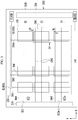
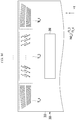
- FIG. 1 and FIG. 2 a display device according to an exemplary embodiment will be described with reference to FIG. 1 and FIG. 2 .
- FIG. 1 is a schematic top plan view of a display device according to an exemplary embodiment
- FIG. 2 is a cross-sectional view taken along a line II-II' of FIG. 1 .
- the display device may include a substrate SUB, a first pad unit PAD_1, and a printed circuit board (PCB) 300.
- a first terminal region TL_1 and a second terminal region TL_2 are formed at a first pad unit PAD_1 of the printed circuit board (PCB) 300, and a plurality of first pad terminals PAD_TL_A (referring to FIG. 5 ) disposed at the first terminal region TL_1 and a plurality of second pad terminals PAD_TL_B (referring to FIG. 6 ) disposed at the second terminal region TL_2 may be formed with different patterns.
- the display device may include a display region DA and a pad region PNL_PAD.
- the display region DA and the pad region PNL_PAD represent a region positioned on the substrate SUB.
- the display region DA is a region displaying an image, and a display panel 100 (referring to FIG. 3 ) emitting light may be disposed in the display region DA.
- the display panel 100 will be described further below.
- the pad region PNL_PAD is a region positioned around the display region DA, and the pad region PNL_PAD may be bonded with the printed circuit board (PCB) 300 so as to transmit signals from an external source.
- the first pad unit PAD_1 is disposed in the pad region PNL_PAD, thereby the first pad unit PAD_1 and the printed circuit board (PCB) 300 may be electrically coupled.
- the first pad unit PAD_1 may include a first terminal region TL_1 and a second terminal region TL_2.
- the first terminal region TL_1 and the second terminal region TL_2 represent a region positioned on the substrate SUB.
- a plurality of first pad terminals PAD_TL_A (referring to FIG. 5 ) may be disposed in the first terminal region TL_1, and a plurality of second pad terminals PAD_TL_B (referring to FIG. 6 ) may be disposed in the second terminal region TL_2.
- the plurality of first pad terminals PAD_TL_A may be disposed with a first pattern in the first terminal region TL_1.
- the plurality of second pad terminals PAD_TL_B may be disposed in the second terminal region TL_2 with the second pattern that is different from the first pattern.
- the pattern represents a shape in which the pad terminals in the first terminal region TL_1 and the second terminal region TL_2 are disposed.
- the plurality of first pad terminals PAD_TL_A and the plurality of second pad terminals PAD_TL_B may be disposed with different shapes in the first terminal region TL_1 and the second terminal region TL_2.
- the structures of the first terminal region TL_1 and the second terminal region TL_2 are described in further detail below.
- the first terminal region TL_1 and the second terminal region TL_2 of the pad region PNL_PAD may be disposed in parallel in the first direction, especially aligned in the first direction.
- the pad region PNL_PAD may be disposed to be separated from the display region DA in the second direction.
- an X-axis and a Y-axis representing coordinates in the drawing represent the first direction and the second direction, respectively.
- the second terminal region TL_2 may be positioned at both sides of the first terminal region TL_1, especially in the first direction.
- the arrangement structures of the first terminal region TL_1 and the second terminal region TL_2 are not limited thereto, and like an exemplary variation shown in FIG. 21 , the second terminal region TL_2 may be disposed between a pair of first terminal regions TL_1, especially in the first direction.
- Connection wiring CL is positioned between the display region DA and the pad region PNL_PAD, and the display region DA and the pad region PNL_PAD may be connected by the connection wiring CL.
- the connection wiring CL may be connected to a plurality of signal lines disposed in the display region DA. Also, the connection wiring CL may be connected with the first pad terminals PAD_TL_A of the pad region PNL_PAD and the plurality of second pad terminals PAD_TL_B.
- connection wiring CL may include first connection wiring CL_A and second connection wiring CL_B.
- the first connection wiring CL_A may connect the display region DA and the first terminal region TL_1 to each other
- the second connection wiring CL_B may connect the display region DA and the second terminal region TL_2 to each other.
- the printed circuit board (PCB) 300 is bonded to the first pad unit PAD_1 of the pad region PNL_PAD of the substrate SUB, thereby transmitting the signal required for driving the display panel 100.
- a driving chip 350 may be mounted on a base film 310 of the printed circuit board (PCB) 300, and the driving chip 350 may be used for driving the display panel 100.
- a second pad unit PAD_2 is formed at one end of a base film 310, and the second pad unit PAD_2 may be bonded to the first pad unit PAD_1 of the substrate SUB.
- the second pad unit PAD_2 may be disposed to face the first pad unit PAD_1.
- the second pad unit PAD_2 may include a third terminal region TL_3 and a fourth terminal region TL_4.
- the third terminal region TL_3 and the fourth terminal region TL_4 represent a region positioned on the base film 310.
- a plurality of third pad terminals PAD_TL_C (referring to FIG. 10 ) may be disposed, and a plurality of fourth pad terminals PAD_TL_D (referring to FIG. 12 ) may be disposed in the fourth terminal region TL_4.
- the plurality of third pad terminals PAD_TL_C may be formed of a third pattern corresponding to the above-described first pattern, in the third terminal region TL_3.
- the third pattern may have a shape that is the same as or similar to the first pattern.
- the plurality of fourth pad terminals PAD_TL_D may be formed of a fourth pattern corresponding to the above-described second pattern, in the fourth terminal region TL_4.
- the fourth pattern may have a shape that is the same as or similar to the second pattern.
- the second pad unit PAD_2 of the printed circuit board (PCB) 300 may be formed in a shape corresponding to the first pad unit PAD_1 of the substrate SUB. That is, the plurality of pad terminals disposed in the second pad unit PAD_2 may be disposed in a pattern that is the same as or similar to that of the first pad unit PAD_1.
- the structures of the third terminal region TL_3 and the fourth terminal region TL_4 will be described in further detail below.
- FIG. 3 is a schematic view showing a display region DA of FIG. 1
- FIG. 4 is a cross-sectional view taken along a line IV-IV' of FIG. 3 .
- the display panel 100 includes first gate wires GW1, second gate wires GW2, data wires DW, a display unit 140, and a pixel 150.
- a gate driver 210 sequentially supplies a scan signal to a first scan lines SC2-SC2n or second scan lines SC1-SC2n-1 included in the first gate wires GW1 and the second gate wires GW2, in response to a control signal supplied from an external control circuit (not shown), for example, a timing controller.
- n is an integer of 1 or more.
- the pixels 150 are selected by a scan signal, thereby sequentially receiving a data signal.
- the gate driver 210 shown in FIG. 3 may be formed in the driving chip 350 on the printed circuit board (PCB) 300, but for convenience of description, just the gate driver 210 is shown in FIG. 3 .
- the first gate wires GW1 are positioned on the substrate SUB with a first insulating layer GI1 interposed thereunder, and extend in the first direction.
- the first gate wires GW1 include a second scan line SC2n-1 and a light emission control line En.
- the second scan line SC2n-1 is connected to the gate driver 210 and is supplied with the scan signal from the gate driver 210.
- the light emission control line En is connected to a light emission control driver 220, and is supplied with the light emission control signal from the light emission control driver 220.
- the light emission control driver 220 shown in FIG. 3 may be formed within the driving chip 350 on the printed circuit board (PCB) 300 like the gate driver 210, but for convenience of description, just the light emission control driver 220 is shown in FIG. 3 .
- the second gate wires GW2 are positioned on the first gate wires GW1 via a second insulating layer GI2 interposed therebetween, and extend in the first direction.
- the second gate wires GW2 include a first scan line SC2n and an initialization power line Vinit.
- the first gate wires GW1 and the second gate wires GW2 do not overlap each other, but are instead placed in alternating order.
- the first scan line SC2n is connected to the gate driver 210 and is supplied with the scan signal from the gate driver 210.
- the initialization power line Vinit is connected to the gate driver 210 and receives initialization power from the gate driver 210.
- the initialization power line Vinit receives initialization power from the gate driver 210, however the initialization power line Vinit may be connected to an additional configuration to receive initialization power from the additional configuration.
- the light emission control driver 220 sequentially supplies the light emission control signal to the light emission control line EA-En in response to a control signal supplied from an external component such as a timing controller.
- a control signal supplied from an external component such as a timing controller.
- the light emission control signal controls a light emission time of the pixel 150.
- the light emission control driver 220 may be omitted depending on the configuration of the pixel 150.
- a data driver 230 supplies the data signal to the data line DAm among the data wires DW, in response to a control signal supplied from an external component such as a timing controller.
- the data signal supplied to the data line DAm is supplied to the pixel 150 selected by the scan signal whenever the scan signal is supplied to a particular scan line SC among the first scan lines SC2n and the second scan lines SC2n-1.
- the pixel 150 charges the voltage corresponding to the data signal and emits a luminance corresponding thereto.
- the data driver 230 shown in FIG. 3 may be formed in the driving chip 350 on the printed circuit board (PCB) 300, but for convenience of explanation, only the data driver 230 is shown in FIG. 3 .
- the data wires DW are positioned on the second gate wires GW2 via the third insulating layer ILD interposed therebetween, and extend in the second direction crossing the first direction.
- the data wires DW include data lines DA1-DAm and a driving power line ELVDDL.
- Each data line DAm is connected to the data driver 230 and receives data signals from the data driver 230.
- the driving power line ELVDDL is connected to an external first power source ELVDD that will be described later, and receives driving power from the first power source ELVDD.
- the driving power line ELVDDL and the data line DAm may be formed from, or on, the same layer on the third insulating layer ILD.
- the present invention is not limited thereto, and the driving power line ELVDDL and the data line DAm may be formed from, or on, different layers.
- the driving power line ELVDDL may be formed from the same layer as the first gate wire GW1, and the data line DAm may be formed from the same layer as the second gate wire GW2.
- the driving power line ELVDDL may be formed from the same layer as the second gate wire GW2, and the data line DAm may be formed from the same layer as the first gate wire GW1.
- the display unit 140 includes a plurality of pixels 150 positioned at crossings of the first gate wires GW1, the second gate wires GW2, and the data wires DW.
- each pixel 150 includes an organic light emitting element that emits light of a luminance corresponding to a driving current corresponding to the data signal, and a pixel circuit to control the driving current flowing to the organic light emitting element.
- the pixel circuit is respectively connected to the first gate wires GW1, the second gate wires GW2, and the data wires DW, and the organic light emitting element is connected to the pixel circuit.
- the pixel 150 is described as an organic light emitting element, however the pixel 150 applied to the display device of the present exemplary embodiment is not limited thereto, and it may be for example a liquid crystal display element or an electrophoretic display element.
- the organic light emitting element of the display unit 140 is connected to the external first power source ELVDD via the pixel circuit interposed therebetween, and is also connected to a second power source ELVSS.
- the first power source ELVDD and the second power source ELVSS respectively supply driving power and common power to the pixel 150 of the display unit 140, and the pixel 150 emits light with a luminance corresponding to the driving current from the first power source ELVDD and the second source ELVSS.
- the first gate wires GW1 and the second gate wires GW2 transverse the pixel 150 in the first direction and do not overlap each other. They are not positioned at the same layer either, but instead the first gate wires GW1 and the second gate wires GW2 are respectively positioned at different layers from each other via the second insulating layer GI2, and accordingly a distance W between adjacent gate wires may be decreased, thereby forming more pixels 150 in the same area. That is, a high resolution display device may be formed.
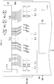
- FIG. 5 is an enlarged view of a first terminal region TL_1 of FIG. 1 .
- a plurality of first pad terminals PAD_TL_A may be disposed in the first terminal region TL_1.
- the first terminal region TL_1 may be connected to the data wires DW of the display region DA through the first connection wiring CL_A.
- the plurality of first pad terminals PAD_TL_A may be disposed to be separated by a predetermined interval in the first direction within the first terminal region TL_1.
- the plurality of first pad terminals PAD_TL_A may respectively include first column sub-pad terminals ROW_PAD_A, second column sub-pad terminals ROW_PAD_B, and first terminal connection lines TL_CN_A.
- a plurality of first column sub-pad terminals ROW_PAD_A_1 to ROW_PAD_A_4 defines a line or column
- a plurality of second column sub-pad terminals ROW_PAD_B_1 to ROW_PAD_B_4 defines a line or column, wherein the different columns are connected by a connection line TL_CN_A_1 to TL_CN_A_4, respectively.
- first column sub-pad terminals ROW_PAD_A may be disposed to be separated from each other in one direction.
- first column sub-pad terminals ROW_PAD_A may form a first inclination angle ⁇ 1 with the first direction. That is, the first column sub-pad terminals ROW_PAD_A may be arranged along a line that is inclined at the first inclination angle ⁇ 1 with respect to the first direction.
- the first inclination angle ⁇ 1 may be in a range of 0 degrees to 90 degrees (excluding 0 degrees and 90 degrees).
- a plurality or all first column sub-pad terminals ROW_PAD_A respectively the columns or lines defined by them disposed in the first terminal region TL_1 may be disposed to be inclined in the same direction. That is, a plurality or all first column sub-pad terminals ROW_PAD_A respectively the columns and lines formed thereby may be inclined at the same angle with respect to the X-axis, in the first terminal region TL_1. For example, as shown in FIG. 1 , the first column sub-pad terminals ROW_PAD_A may be inclined at an approximate 1 o'clock direction.
- first column sub-pad terminals ROW_PAD_A may be disposed inclined to each other, for example at least two different lines or columns of first column sub-pad terminals ROW_PAD_A or two groups of lines or columns of different first column sub-pad terminals ROW_PAD_A may be positioned mirrored to each other, with a symmetry axis in the second direction.
- a part of the first column sub-pad terminals ROW_PAD_A disposed in the first terminal region TL_1 may be disposed to be inclined in an approximate 11 o'clock direction.
- the rest of the first column sub-pad terminals ROW_PAD_A may be disposed to be inclined in the approximate 1 o'clock direction.
- the interval between adjacent first column sub-pad terminals ROW_PAD_A may be constant.
- the first column sub-pad terminals ROW_PAD_A may be formed with an approximate quadrangular shape.
- the second column sub-pad terminals ROW_PAD_B may be disposed to be separated from the first column sub-pad terminals ROW_PAD_A in the second direction. Like the first column sub-pad terminals ROW_PAD_A, the second column sub-pad terminals ROW_PAD_B may be disposed to be separated from each other in one direction.
- the second column sub-pad terminals ROW_PAD_B may form a second inclination angle ⁇ 2 with the first direction. That is, the second column sub-pad terminals ROW_PAD_B may be arranged along a line that is inclined at the second inclination angle ⁇ 2 with respect to the first direction.
- the second inclination angle ⁇ 2 may be in the range of 0 degrees to 90 degrees (excluding 0 degrees and 90 degrees).
- a plurality or all second column sub-pad terminals ROW_PAD_B respectively the columns or lines defined by them disposed in the first terminal region TL_1 may be disposed to be inclined in the same direction, like the first column sub-pad terminals ROW_PAD_A.
- a plurality or all second column sub-pad terminals ROW_PAD_B respectively the columns and lines formed thereby may be disposed to be inclined at the same angle with respect to the X-axis within the first terminal region TL_1.
- the second column sub-pad terminals ROW_PAD_B may be disposed to be inclined at an approximate 1 o'clock direction.
- part of the second column sub-pad terminals ROW_PAD_B disposed in the first terminal region TL_1 may be disposed to be inclined at an approximate 11 o'clock direction.
- the rest of the second column sub-pad terminals ROW_PAD_B may be disposed in the approximate 1 o'clock direction.
- the first inclination angle ⁇ 1 and the second inclination angle ⁇ 2 may be equal. Accordingly, the first column sub-pad terminals ROW_PAD_A and the second column sub-pad terminals ROW_PAD_B may be disposed to be inclined at the same angle with respect to the first direction. However, the present invention is not limited thereto, and the first inclination angle ⁇ 1 and the second inclination angle ⁇ 2 may be different from each other. Accordingly, the first column sub-pad terminals ROW_PAD_A and the second column sub-pad terminals ROW_PAD_B may be arranged to be inclined at different angles from each other with respect to the first direction.
- the plurality of first pad terminals PAD_TL_A disposed in the first terminal region TL_1 may be disposed to be inclined in the same direction. That is, the first column sub-pad terminals ROW_PAD_A and the second column sub-pad terminals ROW_PAD_B, making up the plurality of first pad terminals PAD_TL_A, may all be disposed to be inclined at the same angle with respect to the X-axis.
- a plurality of first pad terminals PAD_TL_A disposed in the first terminal region TL_1 may be disposed to be symmetric to each other with respect to a center region of the first terminal region TL_1, especially with respect to a symmetry line in the second direction.
- a plurality of first pad terminals PAD_TL_A disposed in the first terminal region TL_1 may be disposed to be symmetric to each other with respect to a center region, especially with respect to a symmetry line in the second direction, of a part or section of the first terminal region TL_1 in the first direction disposed between parts or sections of the second terminal region TL_2.
- the plurality of first pad terminals PAD_TL_A to the left of the center region of the first terminal region TL_1 may be inclined at an approximate 1 o'clock direction
- the plurality of first pad terminals PAD_TL_A to the right of the center region of the first terminal region TL_1 may be inclined at an approximate 11 o'clock direction.
- the interval between the adjacent second column sub-pad terminals ROW_PAD_B may be constant.
- the interval between the second column sub-pad terminal ROW_PAD_B_1 and the second column sub-pad terminal ROW_PAD_B_2 the interval between the second column sub-pad terminal ROW_PAD_B_2 and the second column sub-pad terminal ROW_PAD_B_3, and the interval between the second column sub-pad terminal ROW_PAD_B_3 and the second column sub-pad terminal ROW_PAD_B_4 may be equal.
- the second column sub-pad terminals ROW_PAD_B may have a substantially quadrangular shape.
- the quadrangle forming each shape of the first column sub-pad terminals ROW_PAD_A and the second column sub-pad terminals ROW_PAD_B may include a first side L1 parallel to the first direction (the X-axis) and a second side L2 parallel to the second direction (the Y-axis).
- the first side L1 and the second side L2 may be adjacent to each other.
- the second side L2 may be longer than the first side L1 (L1 ⁇ L2). That is, the quadrangle may have a rectangular shape that is elongated in the second direction (the Y-axis).
- the interval between the first column sub-pad terminals ROW_PAD_A or the second column sub-pad terminals ROW_PAD_B in the first direction may be reduced in comparison to an embodiment with square column sub-pad terminals.
- first column sub-pad terminals ROW_PAD_A and second column sub-pad terminals ROW_PAD_B disposed in the first terminal region TL_1 may be increased.
- the plurality of first column sub-pad terminals ROW_PAD_A and the plurality of second column sub-pad terminals ROW_PAD_B may be connected by a plurality of first terminal connection lines TL_CN_A.
- each of the first terminal connection lines TL_CN_A may connect one among the plurality of first column sub-pad terminals ROW_PAD_A and one among the plurality of second column sub-pad terminals ROW_PAD_B.
- first column sub-pad terminal ROW_PAD_A_1 and the second column sub-pad terminal ROW_PAD_B_1 may be connected to each other by the first terminal connection line TL_CN_A_1, and the first column sub-pad terminal ROW_PAD_A_2 and the second column sub-pad terminal ROW_PAD_B_2 may be connected to each other by the first terminal connection line TL_CN_A_2.
- first column sub-pad terminal ROW_PAD_A_3 and the second column sub-pad terminal ROW_PAD_B_3 may be connected to each other by the first terminal connection line TL_CN_A_3, and the first column sub-pad terminal ROW_PAD_A_4 and the second column sub-pad terminal ROW_PAD_B_4 may be connected to each other by the first terminal connection line TL_CN_A_4.
- the plurality of first terminal connection lines TL_CN_A may have a shape that is bent at least one time.
- the first terminal connection line TL_CN_A_1 extends from the second column sub-pad terminal ROW_PAD_B_1 to the first column sub-pad terminal ROW_PAD_A_1 along the second direction.
- the first terminal connection line TL_CN_A_1 may be disposed in a shape that is bent in the first direction, and then is again bent in the second direction. That is, the first terminal connection line TL_CN_A_1 may be disposed in a shape that is bent two times.
- first column sub-pad terminals ROW_PAD_A may be connected to the first connection wiring CL_A.
- the first column sub-pad terminal ROW_PAD_A_1 may be connected with the first connection wiring CL_A_1
- the first column sub-pad terminal ROW_PAD_A_2 may be connected with first connection wiring CL_A_2.
- the first column sub-pad terminal ROW_PAD_A_3 may be connected with the first connection wiring CL_A_3, and the first column sub-pad terminal ROW_PAD_A_4 may be connected with the first connection wiring CL_A_4.
- At least one first dummy pad terminal DM_TL_A may be disposed between a pair of adjacent first column sub-pad terminals ROW_PAD_A.
- one first dummy pad terminal DM_TL_A may be disposed between the first column sub-pad terminal ROW_PAD_A_1 and the first column sub-pad terminal ROW_PAD_A_2
- one first dummy pad terminal DM_TL_A_2 may be disposed between the first column sub-pad terminal ROW_PAD_A_2 and the first column sub-pad terminal ROW_PAD_A_3.
- One first dummy pad terminal DM_TL_A_3 may be disposed between the first column sub-pad terminal ROW_PAD_A_3 and the first column sub-pad terminal ROW_PAD_A_4, and one first dummy pad terminal DM_TL_A_4 may be disposed close to the first column sub-pad terminal ROW_PAD_A_4.
- FIG. 5 shows that one first dummy pad terminal DM_TL_A is disposed between a pair of adjacent first column sub-pad terminals ROW_PAD_A.
- the present invention is not limited thereto, and two or more first dummy pad terminals DM_TL_A may be disposed between adjacent first column sub-pad terminals ROW_PAD_A.
- the first column sub-pad terminals ROW_PAD_A and the first dummy pad terminals DM_TL_A may be disposed to be parallel to each other. That is, the first column sub-pad terminals ROW_PAD_A and the first dummy pad terminals DM_TL_A may all be arranged along the same line, and may be disposed to be inclined at the first inclination angle ⁇ 1 with respect to the first direction.
- At least one first dummy pad terminal DM_TL_A may be disposed between a pair of adjacent first column sub-pad terminals ROW_PAD_A, the distance between the adjacent first column sub-pad terminals ROW_PAD_A is increased such that capacitive bonding, that is, capacitive coupling generated between adjacent first column sub-pad terminals ROW_PAD_A, may be prevented.
- At least one second dummy pad terminal DM_TL_B may be disposed between a pair of adjacent second column sub-pad terminals ROW_PAD_B.
- one second dummy pad terminal DM_TL_B_1 may be disposed between the second column sub-pad terminal ROW_PAD_B_1 and the second column sub-pad terminal ROW_PAD_B_2
- one second dummy pad terminal DM_TL_B_2 may be disposed between the second column sub-pad terminal ROW_PAD_B_2 and the second column sub-pad terminal ROW_PAD_B_3.
- One second dummy pad terminal DM_TL_B_3 may be disposed between the second column sub-pad terminal ROW_PAD_B_3 and the second column sub-pad terminal ROW_PAD_B_4, and one second dummy pad terminal DM_TL_B_4 may be disposed adjacent to the second column sub-pad terminal ROW_PAD_B_4.
- FIG. 5 shows that one second dummy pad terminal DM_TL_B is disposed between a pair of adjacent second column sub-pad terminals ROW_PAD_B.
- the present invention is not limited thereto, and two or more second dummy pad terminals DM_TL_B may be disposed between adjacent second column sub-pad terminals ROW_PAD_B.
- the second column sub-pad terminals ROW_PAD_B and the second dummy pad terminals DM_TL_B may be disposed to be parallel to each other. That is, the second column sub-pad terminals ROW_PAD_B and the second dummy pad terminals DM_TL_B may all be arranged along one line, which is inclined at the second inclination angle ⁇ 2 with respect to the first direction.
- first column sub-pad terminals ROW_PAD_A and the second column sub-pad terminals ROW_PAD_B are disposed to be inclined at the predetermined angle with respect to the first direction, many pad terminals may be disposed in a predetermined area.
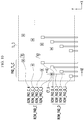
- FIG. 6 is an enlarged view of a second terminal region TL_2 of FIG. 1 .
- a plurality of second pad terminals PAD_TL_B may be disposed in the second terminal region TL_2.
- the second terminal region TL_2 may be connected to power lines, for example, the driving power line ELVDDL, the common power line, the initialization power line, the scan line, and the like disposed in the display region DA through the second connection wiring CL_B.
- the plurality of second pad terminals PAD_TL_B may be disposed to be separated from each other at a predetermined interval in the first direction within the second terminal region TL_2.
- the plurality of second pad terminals PAD_TL_B may each include a pair of second sub-pad terminals SUB_PAD_B and a second terminal connection line TL_CN_B.
- a pair of second sub-pad terminals SUB_PAD_B may be disposed to be separated from each other in one direction.
- a pair of second sub-pad terminals SUB_PAD_B_1 and SUB_PAD_B_2 may be disposed to be separated from each other in the second direction.
- a pair of second sub-pad terminals SUB_PAD_B_1 and SUB_PAD_B_2 may be arranged in one line along the second direction.
- the second sub-pad terminal SUB_PAD_B may be formed to have an approximate quadrangular shape.
- the second sub-pad terminal SUB_PAD_B may have a rectangular shape that is elongated in the second direction.
- the second sub-pad terminals SUB_PAD_B_1 and SUB_PAD_B_2 are each formed with a rectangular shape having long sides and short sides that are adjacent to each other, and the length of the long sides is larger than the length of the short sides by two times or more.
- a pair of second sub-pad terminals SUB_PAD_B may be connected by a second terminal connection line TL_CN_B. That is, the second terminal connection lines TL_CN_B may be positioned between the second sub-pad terminals SUB_PAD_B_1 and the second sub-pad terminals SUB_PAD_B_2, so that the second sub-pad terminals SUB_PAD_B_1 and respective second sub-pad terminals SUB_PAD_B_2 may be electrically connected.
- the second terminal connection line TL_CN_B may be disposed in a straight line. Different from the above-described first terminal connection lines TL_CN_A, the second terminal connection line TL_CN_B does not have a bent shape, but may instead simply be disposed in a straight line. Accordingly, a pair of second sub-pad terminals SUB_PAD_B and the corresponding second terminal connection line TL_CN_B may be arranged in one line.
- the second sub-pad terminals SUB_PAD_B_1 may be connected to the second connection wiring CL_B. Accordingly, the second sub-pad terminals SUB_PAD_B_1 may be connected to the power lines disposed in the display region DA through the second connection wiring CL_B. For example, the second sub-pad terminals SUB_PAD_B_1 may be electrically connected to the driving power line or the common power line, and the like, through the second connection wiring CL_B.
- a plurality of second pad terminals PAD_TL_B is connected to the driving power line or the common power line, thereby preventing a luminance reduction of the image displayed in the display device.
- the second pad terminal PAD_TL_B may include a straight-shaped second terminal connection line TL_CN_B. That is, the second terminal connection line TL_CN_B is disposed as a straight line that is not bent, such that the increase in resistance of the wiring due to having a bent shape does not appear. Accordingly, as the increase in resistance of the wiring is prevented, the reduction of the luminance generated in the display device may be prevented.
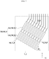
- a plurality of second pad terminals PAD_TL_B' may be disposed in the second terminal region TL_2.
- the plurality of second pad terminals PAD_TL_B' may respectively include a pair of second sub-pad terminals SUB_PAD_B' and a second terminal connection line TL_CN_B'.
- Each pair of second sub-pad terminals SUB_PAD_B' may be disposed in one direction to be separated from each other.
- a pair of second sub-pad terminals SUB_PAD_B_1' and SUB_PAD_B_2' may be arranged to be inclined at a third inclination angle ⁇ 3 with respect to the first direction.
- the second sub-pad terminals SUB_PAD_B_1' and SUB_PAD_B_2' may be disposed one behind another on a line inclined at the third inclination angle ⁇ 3.
- the third inclination angle ⁇ 3 may be in the range of 0 degrees to 90 degrees (excluding 0 degrees and 90 degrees).
- the third inclination angle ⁇ 3 may be the same or different to the first inclination angle ⁇ 1 and or the second inclination angle ⁇ 2.
- a pair of second sub-pad terminals SUB_PAD_B' may be connected by a second terminal connection line TL_CN_B'. That is, the second terminal connection lines TL_CN_B' may be positioned between the second sub-pad terminals SUB_PAD_B_1' and the second sub-pad terminals SUB_PAD_B_2'. And the second terminal connection lines TL_CN_B' may electrically connect the second sub-pad terminals SUB_PAD_B_1' and the second sub-pad terminals SUB_PAD_B_2'.
- the second terminal connection line TL_CN_B' may be disposed with a straight shape. Accordingly, a pair of second sub-pad terminals SUB_PAD_B' and a second terminal connection line TL_CN_B' may be arranged along one line. In this case, a pair of second sub-pad terminals SUB_PAD_B' and the second terminal connection line TL_CN_B' may be arranged along a line that is inclined at the third inclination angle ⁇ 3 with respect to the first direction.
- all second sub-pad terminals SUB_PAD_B' may be arranged to be inclined at the same third inclination angle ⁇ 3 with respect to the first direction.
- different pairs of second sub-pad terminals SUB_PAD_B' may be disposed inclined to each other, for example at least two different pairs of second sub-pad terminals SUB_PAD_B' or two different parts or groups of pairs of second sub-pad terminals SUB_PAD_B' may be positioned mirrored to each other with a symmetry axis in the second direction.
- PCB 300 printed circuit board 300 bonded to the display device according to an exemplary embodiment will be described with reference to FIG. 9 to FIG. 14 .
- FIG. 9 is a schematic top plan view of a printed circuit board (PCB) 300 bonded to a display device of FIG. 1
- FIG. 10 is an enlarged view of a third terminal region TL_3 of FIG. 9
- FIG. 11 is a cross-sectional view taken along a line XI-XI' of FIG. 10
- FIG. 12 is an enlarged view of a fourth terminal region TL_4 of FIG. 9
- FIG. 13 is a cross-sectional view taken along a line XIII-XIII' of FIG. 12
- FIG. 14 is a view of an exemplary variation of a fourth terminal region TL_4 of FIG. 12 .
- the printed circuit board (PCB) 300 may include a flexible base film 310, a second pad unit PAD_2, and a driving chip 350.
- the second pad unit PAD_2 may be disposed at one end of the base film 310. According to the present exemplary embodiment, the second pad unit PAD_2 may be made with a shape corresponding to the shape of the above-described first pad unit PAD_1 of the substrate SUB. As the second pad unit PAD_2 of the printed circuit board (PCB) 300 and the first pad unit PAD_1 of the substrate SUB may be formed with shapes corresponding to each other, the first pad unit PAD_1 and the second pad unit PAD_2 may be more easily bonded.
- PCB printed circuit board
- the second pad unit PAD_2 may include a third terminal region TL_3 and a fourth terminal region TL_4.
- the third terminal region TL_3 and the fourth terminal region TL_4 represent regions positioned on the base film 310.
- the third terminal region TL_3 and the fourth terminal region TL_4 may be arranged in parallel along the first direction on the base film 310, especially aligned in the first direction.
- the fourth terminal region TL_4 may be disposed at both sides of the third terminal region TL_3, especially in the first direction.
- the present invention is not limited thereto, and the fourth terminal region TL_4 may instead be disposed between a pair of third terminal regions TL_3, especially in the first direction.
- the arrangement of the third terminal region TL_3 and the fourth terminal region TL_4 is determined depending on the arrangement of the first terminal region TL_1 and the second terminal region TL_2 disposed on the substrate SUB. For example, if the second terminal region TL_2 is disposed at both sides of the first terminal region TL_1, the fourth terminal region TL_4 may be disposed at both sides of the third terminal region TL_3. Further, if the second terminal region TL_2 is disposed between a pair of first terminal regions TL_1, the fourth terminal region TL_4 may be disposed between a pair of third terminal regions TL_3.
- the third terminal region TL_3 is a region corresponding to the first terminal region TL_1 of the substrate SUB, and a plurality of third pad terminals PAD_TL_C may be disposed in the third terminal region TL_3.
- the plurality of third pad terminals PAD_TL_C may be disposed in the same pattern as the first pad terminals PAD_TL_A disposed in the above-described first terminal region TL_1. That is, the plurality of third pad terminals PAD_TL_C of the third terminal region TL_3 may be formed with a third pattern corresponding to the above-described first pattern.
- the plurality of third pad terminals PAD_TL_C may include third column sub-pad terminals ROW_PAD_C and fourth column sub-pad terminals ROW_PAD_D.
- the explanations in connection with the first pad terminals PAD_TL_A respectively the first and second column sub-pad terminals ROW_PAD_A, ROW_PAD_B also apply in connection with the third pad terminals PAD_TL_C and the third and fourth column sub-pad terminals ROW_PAD_C, ROW_PAD_D.
- the third column sub-pad terminals ROW_PAD_C may be disposed along one direction to be separated from each other.
- the third column sub-pad terminals ROW_PAD_C may form the first inclination angle ⁇ 1 with respect to the first direction.
- the third column sub-pad terminals ROW_PAD_C may be arranged to be inclined at the first inclination angle ⁇ 1 with respect to the first direction. That is, the third column sub-pad terminals ROW_PAD_C may be arranged to be inclined at the same angle as the first column sub-pad terminals ROW_PAD_A of the substrate SUB.
- the first inclination angle ⁇ 1 may be in the range of 0 degrees to 90 degrees (excluding 0 degrees and 90 degrees).
- the interval between adjacent third column sub-pad terminals ROW_PAD_C may be constant.
- the interval between the third column sub-pad terminal ROW_PAD_C_1 and the third column sub-pad terminal ROW_PAD_C_2 and the third column sub-pad terminal ROW_PAD_C_3, and the interval between the third column sub-pad terminal ROW_PAD_C_3 and the third column sub-pad terminal ROW_PAD_C_4 may be equal.
- adjacent third column sub-pad terminals ROW_PAD_C may be arranged at an interval that is equal to the interval between the above-described first column sub-pad terminals ROW_PAD_A.
- the third column sub-pad terminals ROW_PAD_C may be formed with an approximate quadrangular shape.
- the fourth column sub-pad terminals ROW_PAD_D may be disposed to be separated from the third column sub-pad terminals ROW_PAD_C in the second direction. Like the third column sub-pad terminals ROW_PAD_C, the fourth column sub-pad terminals ROW_PAD_D may be disposed to be separated from each other in one direction.
- the fourth column sub-pad terminals ROW_PAD_D may form the second inclination angle ⁇ 2 with respect to the first direction. That is, the fourth column sub-pad terminals ROW_PAD_D may be arranged along a line that is inclined at the second inclination angle ⁇ 2 with respect to the first direction. That is, the fourth column sub-pad terminals ROW_PAD_D may be arranged to be inclined at the same angle as the second column sub-pad terminals ROW_PAD_B of the substrate SUB.
- the second inclination angle ⁇ 2 may be in the range of 0 degrees to 90 degrees (excluding 0 degrees and 90 degrees).
- the first inclination angle ⁇ 1 and the second inclination angle ⁇ 2 may be equal to each other. Accordingly, the third column sub-pad terminals ROW_PAD_C and the fourth column sub-pad terminals ROW_PAD_D may be arranged to be inclined at the same angle with respect to the first direction.
- the present invention is not limited thereto, and the first inclination angle ⁇ 1 and the second inclination angle ⁇ 2 may be different from each other. Accordingly, the third column sub-pad terminals ROW_PAD_C and the fourth column sub-pad terminals ROW_PAD_D may be arranged to be inclined at different angles with the first direction.
- the intervals between the adjacent fourth column sub-pad terminals ROW_PAD_D may be equal to each other.
- the interval between the fourth column sub-pad terminal ROW_PAD_D_1 and the fourth column sub-pad terminal ROW_PAD_D_2 the interval between the fourth column sub-pad terminal ROW_PAD_D_2 and the fourth column sub-pad terminal ROW_PAD_D_3, and the interval between the fourth column sub-pad terminal ROW_PAD_D_3 and the fourth column sub-pad terminal ROW_PAD_D_4 may be equal.
- the fourth column sub-pad terminals ROW_PAD_D may be formed to have an approximate quadrangular shape.
- first terminal wiring P_L_A_1 and the second terminal wiring P_L_B_1 may be positioned at opposing sides of the base film 310 in the printed circuit board (PCB) 300.
- the first terminal wiring P_L_A_1 may be positioned on or over the base film 310, and the second terminal wiring P_L_B_1 may be positioned under the base film 310.
- the first terminal wiring P_L_A_1 and the second terminal wiring P_L_B_1 may be electrically connected to the driving chip 350, respectively.
- a first protection layer SR1 may be disposed on the first terminal wiring P_L_A_1, and a second protection layer SR2 may be disposed on the second terminal wiring P_L_B_1.
- the first protection layer SR1 and the second protection layer SR2 may each be a solder resist.
- the third column sub-pad terminal ROW_PAD_C_1 and the fourth column sub-pad terminal ROW_PAD_D_1 may be formed of the same layer as the second terminal wiring P_L_B_1.
- a part of the second protection layer SR2 is removed such that a part of the second terminal wiring P_L_B_1 may be exposed.
- the third column sub-pad terminal ROW_PAD_C_1 and the fourth column sub-pad terminal ROW_PAD_D_1 are separated from each other.
- the third column sub-pad terminal ROW_PAD_C_1 may be electrically connected to the first terminal wiring P_L_A_1 through a first contact hole CT_1 formed in the base film 310.
- the first contact hole CT_1 may be disposed to overlap the third column sub-pad terminal ROW_PAD_C_1.
- the first contact hole CT_1 is filled with the same metal as the first terminal wiring P_L_A_1, but may instead be filled with the same metal as the third column sub-pad terminal ROW_PAD_C_1.
- the fourth column sub-pad terminal ROW_PAD_D_1 may be formed of the same metal layer as the second terminal wiring P_L_B_1.
- the fourth column sub-pad terminal ROW_PAD_D_1 may correspond to a region where a part of the second terminal wiring P_L_B_1 is exposed.
- the fourth terminal region TL_4 is a region corresponding to the second terminal region TL_2 of the substrate SUB, and a plurality of fourth pad terminals PAD_TL_D may be disposed in the fourth terminal region TL_4.
- the plurality of fourth pad terminals PAD_TL_D may be disposed in the same pattern as the second pad terminals PAD_TL_B disposed in the above-described second terminal region TL_2. That is, the plurality of fourth pad terminals PAD_TL_D of the fourth terminal region TL_4 may be formed in the fourth pattern corresponding to the above-described second pattern.
- the plurality of fourth pad terminals PAD_TL_D may respectively include a pair of fourth sub-pad terminals SUB_PAD_D.
- Each pair of fourth sub-pad terminals SUB_PAD_D may be disposed in one direction to be separated from each other.
- a pair of fourth sub-pad terminals SUB_PAD_D_1 and SUB_PAD_D_2 may be disposed along the second direction to be separated from each other.
- a pair of fourth sub-pad terminals SUB_PAD_D_1 and SUB_PAD_D_2 may be disposed in one line along the second direction.
- the fourth sub-pad terminal SUB_PAD_D may be made to have an approximate quadrangular shape.
- the fourth sub-pad terminal SUB_PAD_D may have a rectangular shape that is elongated in the second direction.
- the fourth sub-pad terminals SUB_PAD_D_1 and SUB_PAD_D_2 have a rectangular shape having adjacent long sides and short sides, and the length of the long sides is larger than the length of the short sides by two times or more.
- the fourth sub-pad terminals SUB_PAD_D_1 and SUB_PAD_D_2 may be formed of the same layer as the second terminal wiring P_L_B_2.
- part of the second protection layer SR2 is removed such that parts of the second terminal wiring P_L_B_1 are exposed.
- the fourth sub-pad terminals SUB_PAD_D_1 and SUB_PAD_D_2 are separated from each other.
- the first terminal wiring P_L_A_2 and the second terminal wiring P_L_B_2 may be positioned at opposing sides of the base film 310 in the printed circuit board (PCB) 300.
- the first terminal wiring P_L_A_2 may be positioned on the base film 310
- the second terminal wiring P_L_B_2 may be positioned under the base film 310.
- the first terminal wiring P_L_A_2 and the second terminal wiring P_L_B_2 may be respectively and electrically connected to the driving chip 350.
- the fourth sub-pad terminal SUB_PAD_D_1 may be electrically connected to the first terminal wiring P_L_A_2 through the second contact hole CT_2 formed in the base film 310.
- the fourth sub-pad terminal SUB_PAD_D_1 and the second contact hole CT_2 are arranged to not overlap each other.
- the second terminal wiring P_L_B_2 may be formed to extend in the second direction from the fourth sub-pad terminal SUB_PAD_D_1.
- the second contact hole CT_2 may overlap the second terminal wiring P_L_B_2.
- the same metal as that of the first terminal wiring P_L_A_2 may be filled in the second contact hole CT_2, or the metal configuring the fourth sub-pad terminal SUB_PAD_D_1 may be filled therein.
- the fourth sub-pad terminal SUB_PAD_D_2 may be formed of the same metal layer as the second terminal wiring P_L_B_2.
- the fourth sub-pad terminal SUB_PAD_D_2 may correspond to a region where part of the second terminal wiring P_L_B_2 is exposed.
- a plurality of fourth pad terminals PAD_TL_D' may be disposed in the fourth terminal region TL_4.
- Each of a plurality of fourth pad terminals PAD_TL_D' may include a pair of fourth sub-pad terminals SUB_PAD_D'.
- a pair of fourth sub-pad terminals SUB_PAD_D' may be disposed in one direction to be separated from each other. However, differently from FIG. 12 , a pair of fourth sub-pad terminals SUB_PAD_D_1' and SUB_PAD_D_2' may be arranged at the third inclination angle ⁇ 3 with respect to the first direction.
- the third inclination angle ⁇ 3 formed by the fourth sub-pad terminals SUB_PAD_D_1' and SUB_PAD_D_2' of FIG. 14 may be the same as the angle formed by the second sub-pad terminal SUB_PAD_B' formed on the substrate SUB of FIG. 7 .
- the explanation above in connection with the third inclination angle ⁇ 3 of the second terminal connection line TL_CN_B' applies also here.
- PCB 300 printed circuit board 300
- FIG. 15 is a view of a first exemplary variation of the printed circuit board (PCB) 300 of FIG. 9
- FIG. 16 is a view of a second exemplary variation of the printed circuit board (PCB) 300 of FIG. 9 .
- the plurality of third pad terminals PAD_TL_C of the third terminal region TL_3 may be disposed with the same pattern as the first pad terminals PAD_TL_A disposed in the first terminal region TL_1 of FIG. 1 .
- the plurality of third pad terminals PAD_TL_C may be disposed to be inclined at the same angle within the third terminal region TL_3. That is, the plurality of third pad terminals PAD_TL_C may be inclined in the approximate 1 o'clock direction.
- the plurality of third pad terminals PAD_TL_C of the third terminal region TL_3 may be disposed with the same pattern as the first pad terminals PAD_TL_A disposed in the first terminal region TL_1 of FIG. 8 .
- the plurality of third pad terminals PAD_TL_C of the third terminal region TL_3 may be disposed to be symmetric to each other with respect to the center region of the third terminal region TL_3.
- the plurality of third pad terminals PAD_TL_C to the left of the center region of the third terminal region TL_3 may be inclined in the approximate 1 o'clock direction
- the plurality of third pad terminals PAD_TL_C to the right of the center region of the third terminal region TL_3 may be inclined in the approximate 11 o'clock direction.
- the plurality of fourth pad terminals PAD_TL_D disposed in the fourth terminal region TL_4 may be disposed at different angles with respect to the first direction (the X-axis). For example, in the fourth terminal region TL_4 positioned at the right side of the third terminal region TL_3, the angle of the fourth pad terminals PAD_TL_D with respect to the X-axis may gradually decrease from the left side to the right side. In contrast, in the fourth terminal region TL_4 positioned at the right side of the third terminal region TL_3, the angle of the fourth pad terminals PAD_TL_D with respect to the X-axis may gradually increase from the left side to the right side.
- the angle of the fourth pad terminals PAD_TL_D with respect to the X-axis may gradually decrease from the right side to the left side.
- the angle of the fourth pad terminals PAD_TL_D with respect to the X-axis may gradually increase from the right side to the left side.
- FIG. 17 is a view schematically showing a state in which a second terminal region TL_2 formed in a substrate SUB and a fourth terminal region TL_4 formed in a printed circuit board (PCB) 300 are bonded
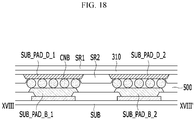
- FIG. 18 is a cross-sectional view taken along a line XVIII-XVIII' of FIG. 17 .
- the second sub-pad terminals SUB_PAD_B_1 and SUB_PAD_B_2 of the second terminal region TL_2, and the fourth sub-pad terminals SUB_PAD_D_1 and SUB_PAD_D_2 of the fourth terminal region TL_4, may be disposed to overlap each other.
- the fourth sub-pad terminal SUB_PAD_D_1 is disposed to overlap the second sub-pad terminal SUB_PAD_B_1, and the fourth sub-pad terminal SUB_PAD_D_2 is disposed to overlap the second sub-pad terminal SUB_PAD_B 2.
- a conductive adhesive film 500 may be disposed between the second terminal region TL_2 and the fourth terminal region TL_4.
- the conductive adhesive film 500 electrically connects the second sub-pad terminals SUB_PAD_B_1 and SUB_PAD_B_2 to the fourth sub-pad terminals SUB_PAD_D_1 and SUB_PAD_D_2.
- the second sub-pad terminals SUB_PAD_B_1 and SUB_PAD_B_2 and the fourth sub-pad terminals SUB_PAD_D_1 and SUB_PAD_D_2 may be electrically connected through a plurality of conductive balls CNB included in the conductive adhesive film 500.
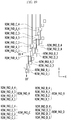
- FIG. 19 is a view schematically showing a state in which a first terminal region TL_1 formed in a substrate SUB and a third terminal region TL_3 formed in a printed circuit board (PCB) 300 are bonded
- FIG. 20 is a cross-sectional view taken along a line XX-XX' of FIG. 19 .
- the third pad terminals PAD_TL_C may be disposed to overlap the first pad terminals PAD_TL_A (referring to FIG. 5 ).
- the third column sub-pad terminals ROW_PAD_C may overlap and be disposed on the first column sub-pad terminals ROW_PAD_A
- the fourth column sub-pad terminals ROW_PAD_D may overlap and be disposed on the second column sub-pad terminals ROW_PAD_B.
- the conductive adhesive film 500 may be disposed between the first terminal region TL_1 and the third terminal region TL_3.
- the conductive adhesive film 500 may electrically connect the first column sub-pad terminals ROW_PAD_A and the third column sub-pad terminals ROW_PAD_C.
- the first column sub-pad terminals ROW_PAD_A and the third column sub-pad terminals ROW_PAD_C may be electrically connected to each other through the plurality of conductive balls CNB included in the conductive adhesive film 500.
- the first terminal region TL_1 and the second terminal region TL_2 are formed in the first pad unit PAD_1, and in this case, the plurality of first pad terminals PAD_TL_A disposed in the first terminal region TL_1 and the plurality of second pad terminals PAD_TL_B disposed in the second terminal region TL_2 may have different patterns from each other.
Landscapes
- Physics & Mathematics (AREA)
- Engineering & Computer Science (AREA)
- Microelectronics & Electronic Packaging (AREA)
- Nonlinear Science (AREA)
- General Physics & Mathematics (AREA)
- Optics & Photonics (AREA)
- Chemical & Material Sciences (AREA)
- Crystallography & Structural Chemistry (AREA)
- Mathematical Physics (AREA)
- Theoretical Computer Science (AREA)
- Computer Hardware Design (AREA)
- Devices For Indicating Variable Information By Combining Individual Elements (AREA)
- Condensed Matter Physics & Semiconductors (AREA)
- Manufacturing & Machinery (AREA)
- Liquid Crystal (AREA)
Applications Claiming Priority (1)
| Application Number | Priority Date | Filing Date | Title |
|---|---|---|---|
| KR1020160088890A KR102732854B1 (ko) | 2016-07-13 | 2016-07-13 | 표시 장치 |
Publications (3)
| Publication Number | Publication Date |
|---|---|
| EP3270218A2 true EP3270218A2 (de) | 2018-01-17 |
| EP3270218A3 EP3270218A3 (de) | 2018-02-07 |
| EP3270218B1 EP3270218B1 (de) | 2024-07-03 |
Family
ID=59655839
Family Applications (1)
| Application Number | Title | Priority Date | Filing Date |
|---|---|---|---|
| EP17181099.7A Active EP3270218B1 (de) | 2016-07-13 | 2017-07-13 | Hochauflösende anzeigevorrichtung |
Country Status (4)
| Country | Link |
|---|---|
| US (2) | US10674605B2 (de) |
| EP (1) | EP3270218B1 (de) |
| KR (1) | KR102732854B1 (de) |
| CN (2) | CN116709852A (de) |
Families Citing this family (17)
| Publication number | Priority date | Publication date | Assignee | Title |
|---|---|---|---|---|
| KR102732854B1 (ko) * | 2016-07-13 | 2024-11-21 | 삼성디스플레이 주식회사 | 표시 장치 |
| KR102567483B1 (ko) * | 2016-09-09 | 2023-08-16 | 삼성디스플레이 주식회사 | 표시 장치 |
| KR102547235B1 (ko) * | 2018-04-20 | 2023-06-23 | 삼성디스플레이 주식회사 | 표시 장치 |
| KR102507222B1 (ko) * | 2018-05-14 | 2023-03-07 | 삼성디스플레이 주식회사 | 표시 장치 |
| KR102745646B1 (ko) * | 2018-11-15 | 2024-12-20 | 엘지디스플레이 주식회사 | 표시 장치 |
| JP2020115173A (ja) * | 2019-01-17 | 2020-07-30 | シャープ株式会社 | 表示装置 |
| WO2020161829A1 (ja) * | 2019-02-06 | 2020-08-13 | シャープ株式会社 | 表示装置 |
| KR102027416B1 (ko) * | 2019-05-31 | 2019-10-01 | (주) 액트 | Led 투명 전광판용 필름기판을 이용한 led 투명 전광판 장치의 제조 방법 |
| CN111383554B (zh) * | 2019-11-06 | 2021-12-17 | 上海中航光电子有限公司 | 显示面板及显示装置 |
| KR102802443B1 (ko) * | 2020-01-10 | 2025-05-07 | 삼성디스플레이 주식회사 | 표시패널, 표시패널의 제조 방법, 및 이를 포함한 표시장치 |
| US11500433B2 (en) * | 2020-01-14 | 2022-11-15 | Au Optronics Corporation | Flexible electronic device |
| KR102363525B1 (ko) * | 2020-01-20 | 2022-02-16 | 주식회사 이브이첨단소재 | Led 투명 전광판용 연성회로기판 |
| CN112180643B (zh) * | 2020-09-25 | 2022-10-21 | 昆山国显光电有限公司 | 阵列基板、显示面板及显示装置 |
| CN114930237A (zh) * | 2020-10-22 | 2022-08-19 | 京东方科技集团股份有限公司 | 显示面板和显示设备 |
| US12408526B2 (en) * | 2020-10-22 | 2025-09-02 | Chengdu Boe Optoelectronics Technology Co., Ltd. | Display panel and display apparatus |
| CN114696129B (zh) * | 2020-12-28 | 2026-03-20 | 超聚变数字技术股份有限公司 | 显示模组及电子设备 |
| CN119451456A (zh) * | 2023-07-28 | 2025-02-14 | 京东方科技集团股份有限公司 | 阵列基板和显示装置 |
Family Cites Families (34)
| Publication number | Priority date | Publication date | Assignee | Title |
|---|---|---|---|---|
| US3720082A (en) * | 1971-09-13 | 1973-03-13 | Kidde Co Presto Lock Div | Combination padlock |
| JPH11202353A (ja) * | 1998-01-09 | 1999-07-30 | Citizen Watch Co Ltd | 液晶表示装置 |
| JP2000321591A (ja) * | 1999-05-14 | 2000-11-24 | Nec Corp | 液晶表示装置 |
| JP3980918B2 (ja) * | 2002-03-28 | 2007-09-26 | 株式会社東芝 | アクティブマトリクス基板及びその製造方法、表示装置 |
| KR100949496B1 (ko) * | 2003-06-30 | 2010-03-24 | 엘지디스플레이 주식회사 | 라인 온 글래스형 액정표시장치 및 그 제조방법 |
| KR20050093606A (ko) * | 2004-03-20 | 2005-09-23 | 삼성에스디아이 주식회사 | 전계 발광 디스플레이 장치 및 이의 제조 방법 |
| KR100671640B1 (ko) * | 2004-06-24 | 2007-01-18 | 삼성에스디아이 주식회사 | 박막 트랜지스터 어레이 기판과 이를 이용한 표시장치와그의 제조방법 |
| JP4662339B2 (ja) * | 2005-02-04 | 2011-03-30 | エプソンイメージングデバイス株式会社 | 液晶表示パネル |
| JP4890100B2 (ja) * | 2006-05-25 | 2012-03-07 | ゲットナー・ファンデーション・エルエルシー | 画像表示装置 |
| JP4816297B2 (ja) * | 2006-07-21 | 2011-11-16 | 三菱電機株式会社 | 実装端子基板及びこれを用いた表示装置 |
| KR101365118B1 (ko) | 2007-02-22 | 2014-02-25 | 삼성디스플레이 주식회사 | 표시 기판과, 이의 제조 방법 및 이를 구비한 표시 장치 |
| WO2009022522A1 (ja) * | 2007-08-10 | 2009-02-19 | Sharp Kabushiki Kaisha | 配線基板、及び、液晶表示装置 |
| TWI368779B (en) * | 2008-02-15 | 2012-07-21 | Chunghwa Picture Tubes Ltd | Peripheral circuit |
| JP5315747B2 (ja) * | 2008-03-27 | 2013-10-16 | 三菱電機株式会社 | 表示装置 |
| TWI370257B (en) * | 2008-07-15 | 2012-08-11 | Au Optronics Corp | Panel circuit structure |
| US8780310B2 (en) | 2008-11-26 | 2014-07-15 | Sharp Kabushiki Kaisha | Display device having higher-layer wiring that does not overlap connection portion |
| EP2355074A4 (de) * | 2008-12-05 | 2012-05-30 | Sharp Kk | Substrat für eine anzeigevorrichtung und anzeigevorrichtung |
| JP2011187217A (ja) | 2010-03-05 | 2011-09-22 | Nippon Seiki Co Ltd | 有機elモジュール |
| KR101802845B1 (ko) * | 2011-02-23 | 2017-11-30 | 삼성디스플레이 주식회사 | 어레이 기판, 이를 갖는 표시 장치 및 이의 제조 방법 |
| KR101891989B1 (ko) | 2012-08-10 | 2018-10-01 | 엘지디스플레이 주식회사 | 가요성 인쇄회로필름 및 그를 이용한 디스플레이 장치 |
| KR101971201B1 (ko) * | 2012-08-20 | 2019-04-23 | 삼성디스플레이 주식회사 | 양면 표시 장치 및 이의 제작 방법 |
| KR101484642B1 (ko) * | 2012-10-24 | 2015-01-20 | 엘지디스플레이 주식회사 | 유기 발광 표시 장치 |
| KR101484681B1 (ko) * | 2012-11-01 | 2015-01-20 | 엘지디스플레이 주식회사 | 유기 발광 표시 장치 |
| KR102081650B1 (ko) * | 2013-04-10 | 2020-02-26 | 엘지디스플레이 주식회사 | 플렉서블 디스플레이 장치 및 그 제조 방법 |
| CA2911045A1 (en) | 2013-05-03 | 2014-11-06 | Gregory Micheal DALTON | System and method used in design, production and operation of metal forming tools |
| JP6168927B2 (ja) | 2013-09-05 | 2017-07-26 | 株式会社ジャパンディスプレイ | 表示装置 |
| KR20150078983A (ko) * | 2013-12-31 | 2015-07-08 | 엘지디스플레이 주식회사 | 칩 온 필름 패키지 |
| KR102334547B1 (ko) * | 2014-06-17 | 2021-12-03 | 삼성디스플레이 주식회사 | 어레이 기판 및 이를 이용한 집적 회로 실장 방법 |
| JP2016004910A (ja) * | 2014-06-17 | 2016-01-12 | キヤノン株式会社 | 有機発光装置 |
| KR20160022416A (ko) | 2014-08-19 | 2016-03-02 | 삼성디스플레이 주식회사 | 표시 장치 및 이의 구동 방법 |
| US9544994B2 (en) | 2014-08-30 | 2017-01-10 | Lg Display Co., Ltd. | Flexible display device with side crack protection structure and manufacturing method for the same |
| KR102322766B1 (ko) * | 2015-09-03 | 2021-11-08 | 삼성디스플레이 주식회사 | 디스플레이 장치 |
| KR102595086B1 (ko) * | 2016-07-08 | 2023-10-27 | 삼성디스플레이 주식회사 | 표시 장치 및 이의 제조 방법 |
| KR102732854B1 (ko) * | 2016-07-13 | 2024-11-21 | 삼성디스플레이 주식회사 | 표시 장치 |
-
2016
- 2016-07-13 KR KR1020160088890A patent/KR102732854B1/ko active Active
-
2017
- 2017-07-12 US US15/648,122 patent/US10674605B2/en active Active
- 2017-07-13 CN CN202310693170.1A patent/CN116709852A/zh active Pending
- 2017-07-13 EP EP17181099.7A patent/EP3270218B1/de active Active
- 2017-07-13 CN CN201710569712.9A patent/CN107623018B/zh active Active
-
2020
- 2020-04-28 US US16/860,906 patent/US11116079B2/en active Active
Non-Patent Citations (1)
| Title |
|---|
| None |
Also Published As
| Publication number | Publication date |
|---|---|
| EP3270218A3 (de) | 2018-02-07 |
| KR20180007738A (ko) | 2018-01-24 |
| US11116079B2 (en) | 2021-09-07 |
| CN116709852A (zh) | 2023-09-05 |
| KR102732854B1 (ko) | 2024-11-21 |
| US20200260579A1 (en) | 2020-08-13 |
| US10674605B2 (en) | 2020-06-02 |
| CN107623018B (zh) | 2023-07-07 |
| CN107623018A (zh) | 2018-01-23 |
| US20180020543A1 (en) | 2018-01-18 |
| EP3270218B1 (de) | 2024-07-03 |
Similar Documents
| Publication | Publication Date | Title |
|---|---|---|
| US11116079B2 (en) | High resolution display device | |
| CN114497169B (zh) | 显示设备 | |
| KR102569967B1 (ko) | 인쇄회로기판 및 이를 포함하는 표시 장치 | |
| KR102725285B1 (ko) | 표시 장치 | |
| EP3261142A1 (de) | Anzeigevorrichtung mit einem biegebereich | |
| KR102518426B1 (ko) | 표시 장치 | |
| CN114885494B (zh) | 印刷电路板封装 | |
| CN107808894B (zh) | 显示装置 | |
| KR101630332B1 (ko) | 구동회로 칩 및 이를 포함하는 표시 장치 |
Legal Events
| Date | Code | Title | Description |
|---|---|---|---|
| PUAI | Public reference made under article 153(3) epc to a published international application that has entered the european phase |
Free format text: ORIGINAL CODE: 0009012 |
|
| STAA | Information on the status of an ep patent application or granted ep patent |
Free format text: STATUS: THE APPLICATION HAS BEEN PUBLISHED |
|
| PUAL | Search report despatched |
Free format text: ORIGINAL CODE: 0009013 |
|
| AK | Designated contracting states |
Kind code of ref document: A2 Designated state(s): AL AT BE BG CH CY CZ DE DK EE ES FI FR GB GR HR HU IE IS IT LI LT LU LV MC MK MT NL NO PL PT RO RS SE SI SK SM TR |
|
| AX | Request for extension of the european patent |
Extension state: BA ME |
|
| AK | Designated contracting states |
Kind code of ref document: A3 Designated state(s): AL AT BE BG CH CY CZ DE DK EE ES FI FR GB GR HR HU IE IS IT LI LT LU LV MC MK MT NL NO PL PT RO RS SE SI SK SM TR |
|
| AX | Request for extension of the european patent |
Extension state: BA ME |
|
| RIC1 | Information provided on ipc code assigned before grant |
Ipc: H01L 21/00 20060101ALN20180104BHEP Ipc: H05K 1/14 20060101ALN20180104BHEP Ipc: H01L 27/32 20060101ALN20180104BHEP Ipc: G02F 1/1345 20060101AFI20180104BHEP Ipc: G09G 3/00 20060101ALN20180104BHEP |
|
| STAA | Information on the status of an ep patent application or granted ep patent |
Free format text: STATUS: REQUEST FOR EXAMINATION WAS MADE |
|
| 17P | Request for examination filed |
Effective date: 20180807 |
|
| RBV | Designated contracting states (corrected) |
Designated state(s): AL AT BE BG CH CY CZ DE DK EE ES FI FR GB GR HR HU IE IS IT LI LT LU LV MC MK MT NL NO PL PT RO RS SE SI SK SM TR |
|
| STAA | Information on the status of an ep patent application or granted ep patent |
Free format text: STATUS: EXAMINATION IS IN PROGRESS |
|
| 17Q | First examination report despatched |
Effective date: 20200827 |
|
| P01 | Opt-out of the competence of the unified patent court (upc) registered |
Effective date: 20230516 |
|
| GRAP | Despatch of communication of intention to grant a patent |
Free format text: ORIGINAL CODE: EPIDOSNIGR1 |
|
| STAA | Information on the status of an ep patent application or granted ep patent |
Free format text: STATUS: GRANT OF PATENT IS INTENDED |
|
| RIC1 | Information provided on ipc code assigned before grant |
Ipc: H10K 59/10 20230101ALN20240227BHEP Ipc: H05K 1/14 20060101ALN20240227BHEP Ipc: H05K 1/11 20060101ALN20240227BHEP Ipc: H01L 21/00 20060101ALN20240227BHEP Ipc: G09G 3/20 20060101ALN20240227BHEP Ipc: G09G 3/00 20060101ALN20240227BHEP Ipc: G02F 1/1345 20060101AFI20240227BHEP |
|
| RIC1 | Information provided on ipc code assigned before grant |
Ipc: H10K 59/10 20230101ALN20240305BHEP Ipc: H05K 1/14 20060101ALN20240305BHEP Ipc: H05K 1/11 20060101ALN20240305BHEP Ipc: H01L 21/00 20060101ALN20240305BHEP Ipc: G09G 3/20 20060101ALN20240305BHEP Ipc: G09G 3/00 20060101ALN20240305BHEP Ipc: G02F 1/1345 20060101AFI20240305BHEP |
|
| INTG | Intention to grant announced |
Effective date: 20240321 |
|
| GRAS | Grant fee paid |
Free format text: ORIGINAL CODE: EPIDOSNIGR3 |
|
| GRAA | (expected) grant |
Free format text: ORIGINAL CODE: 0009210 |
|
| STAA | Information on the status of an ep patent application or granted ep patent |
Free format text: STATUS: THE PATENT HAS BEEN GRANTED |
|
| AK | Designated contracting states |
Kind code of ref document: B1 Designated state(s): AL AT BE BG CH CY CZ DE DK EE ES FI FR GB GR HR HU IE IS IT LI LT LU LV MC MK MT NL NO PL PT RO RS SE SI SK SM TR |
|
| REG | Reference to a national code |
Ref country code: CH Ref legal event code: EP |
|
| REG | Reference to a national code |
Ref country code: DE Ref legal event code: R096 Ref document number: 602017082943 Country of ref document: DE |
|
| REG | Reference to a national code |
Ref country code: LT Ref legal event code: MG9D |
|
| REG | Reference to a national code |
Ref country code: NL Ref legal event code: MP Effective date: 20240703 |
|
| PG25 | Lapsed in a contracting state [announced via postgrant information from national office to epo] |
Ref country code: PT Free format text: LAPSE BECAUSE OF FAILURE TO SUBMIT A TRANSLATION OF THE DESCRIPTION OR TO PAY THE FEE WITHIN THE PRESCRIBED TIME-LIMIT Effective date: 20241104 |
|
| REG | Reference to a national code |
Ref country code: AT Ref legal event code: MK05 Ref document number: 1700438 Country of ref document: AT Kind code of ref document: T Effective date: 20240703 |
|
| PG25 | Lapsed in a contracting state [announced via postgrant information from national office to epo] |
Ref country code: NL Free format text: LAPSE BECAUSE OF FAILURE TO SUBMIT A TRANSLATION OF THE DESCRIPTION OR TO PAY THE FEE WITHIN THE PRESCRIBED TIME-LIMIT Effective date: 20240703 |
|
| PG25 | Lapsed in a contracting state [announced via postgrant information from national office to epo] |
Ref country code: PT Free format text: LAPSE BECAUSE OF FAILURE TO SUBMIT A TRANSLATION OF THE DESCRIPTION OR TO PAY THE FEE WITHIN THE PRESCRIBED TIME-LIMIT Effective date: 20241104 Ref country code: NL Free format text: LAPSE BECAUSE OF FAILURE TO SUBMIT A TRANSLATION OF THE DESCRIPTION OR TO PAY THE FEE WITHIN THE PRESCRIBED TIME-LIMIT Effective date: 20240703 |
|
| PG25 | Lapsed in a contracting state [announced via postgrant information from national office to epo] |
Ref country code: NO Free format text: LAPSE BECAUSE OF FAILURE TO SUBMIT A TRANSLATION OF THE DESCRIPTION OR TO PAY THE FEE WITHIN THE PRESCRIBED TIME-LIMIT Effective date: 20241003 |
|
| PG25 | Lapsed in a contracting state [announced via postgrant information from national office to epo] |
Ref country code: PL Free format text: LAPSE BECAUSE OF FAILURE TO SUBMIT A TRANSLATION OF THE DESCRIPTION OR TO PAY THE FEE WITHIN THE PRESCRIBED TIME-LIMIT Effective date: 20240703 Ref country code: FI Free format text: LAPSE BECAUSE OF FAILURE TO SUBMIT A TRANSLATION OF THE DESCRIPTION OR TO PAY THE FEE WITHIN THE PRESCRIBED TIME-LIMIT Effective date: 20240703 Ref country code: GR Free format text: LAPSE BECAUSE OF FAILURE TO SUBMIT A TRANSLATION OF THE DESCRIPTION OR TO PAY THE FEE WITHIN THE PRESCRIBED TIME-LIMIT Effective date: 20241004 |
|
| PG25 | Lapsed in a contracting state [announced via postgrant information from national office to epo] |
Ref country code: BG Free format text: LAPSE BECAUSE OF FAILURE TO SUBMIT A TRANSLATION OF THE DESCRIPTION OR TO PAY THE FEE WITHIN THE PRESCRIBED TIME-LIMIT Effective date: 20240703 |
|
| PG25 | Lapsed in a contracting state [announced via postgrant information from national office to epo] |
Ref country code: LV Free format text: LAPSE BECAUSE OF FAILURE TO SUBMIT A TRANSLATION OF THE DESCRIPTION OR TO PAY THE FEE WITHIN THE PRESCRIBED TIME-LIMIT Effective date: 20240703 |
|
| PG25 | Lapsed in a contracting state [announced via postgrant information from national office to epo] |
Ref country code: AT Free format text: LAPSE BECAUSE OF FAILURE TO SUBMIT A TRANSLATION OF THE DESCRIPTION OR TO PAY THE FEE WITHIN THE PRESCRIBED TIME-LIMIT Effective date: 20240703 Ref country code: IS Free format text: LAPSE BECAUSE OF FAILURE TO SUBMIT A TRANSLATION OF THE DESCRIPTION OR TO PAY THE FEE WITHIN THE PRESCRIBED TIME-LIMIT Effective date: 20241103 |
|
| PG25 | Lapsed in a contracting state [announced via postgrant information from national office to epo] |
Ref country code: CZ Free format text: LAPSE BECAUSE OF FAILURE TO SUBMIT A TRANSLATION OF THE DESCRIPTION OR TO PAY THE FEE WITHIN THE PRESCRIBED TIME-LIMIT Effective date: 20240703 Ref country code: HR Free format text: LAPSE BECAUSE OF FAILURE TO SUBMIT A TRANSLATION OF THE DESCRIPTION OR TO PAY THE FEE WITHIN THE PRESCRIBED TIME-LIMIT Effective date: 20240703 |
|
| PG25 | Lapsed in a contracting state [announced via postgrant information from national office to epo] |
Ref country code: ES Free format text: LAPSE BECAUSE OF FAILURE TO SUBMIT A TRANSLATION OF THE DESCRIPTION OR TO PAY THE FEE WITHIN THE PRESCRIBED TIME-LIMIT Effective date: 20240703 Ref country code: RS Free format text: LAPSE BECAUSE OF FAILURE TO SUBMIT A TRANSLATION OF THE DESCRIPTION OR TO PAY THE FEE WITHIN THE PRESCRIBED TIME-LIMIT Effective date: 20241003 |
|
| PG25 | Lapsed in a contracting state [announced via postgrant information from national office to epo] |
Ref country code: RS Free format text: LAPSE BECAUSE OF FAILURE TO SUBMIT A TRANSLATION OF THE DESCRIPTION OR TO PAY THE FEE WITHIN THE PRESCRIBED TIME-LIMIT Effective date: 20241003 Ref country code: PL Free format text: LAPSE BECAUSE OF FAILURE TO SUBMIT A TRANSLATION OF THE DESCRIPTION OR TO PAY THE FEE WITHIN THE PRESCRIBED TIME-LIMIT Effective date: 20240703 Ref country code: NO Free format text: LAPSE BECAUSE OF FAILURE TO SUBMIT A TRANSLATION OF THE DESCRIPTION OR TO PAY THE FEE WITHIN THE PRESCRIBED TIME-LIMIT Effective date: 20241003 Ref country code: LV Free format text: LAPSE BECAUSE OF FAILURE TO SUBMIT A TRANSLATION OF THE DESCRIPTION OR TO PAY THE FEE WITHIN THE PRESCRIBED TIME-LIMIT Effective date: 20240703 Ref country code: IS Free format text: LAPSE BECAUSE OF FAILURE TO SUBMIT A TRANSLATION OF THE DESCRIPTION OR TO PAY THE FEE WITHIN THE PRESCRIBED TIME-LIMIT Effective date: 20241103 Ref country code: HR Free format text: LAPSE BECAUSE OF FAILURE TO SUBMIT A TRANSLATION OF THE DESCRIPTION OR TO PAY THE FEE WITHIN THE PRESCRIBED TIME-LIMIT Effective date: 20240703 Ref country code: GR Free format text: LAPSE BECAUSE OF FAILURE TO SUBMIT A TRANSLATION OF THE DESCRIPTION OR TO PAY THE FEE WITHIN THE PRESCRIBED TIME-LIMIT Effective date: 20241004 Ref country code: FI Free format text: LAPSE BECAUSE OF FAILURE TO SUBMIT A TRANSLATION OF THE DESCRIPTION OR TO PAY THE FEE WITHIN THE PRESCRIBED TIME-LIMIT Effective date: 20240703 Ref country code: ES Free format text: LAPSE BECAUSE OF FAILURE TO SUBMIT A TRANSLATION OF THE DESCRIPTION OR TO PAY THE FEE WITHIN THE PRESCRIBED TIME-LIMIT Effective date: 20240703 Ref country code: CZ Free format text: LAPSE BECAUSE OF FAILURE TO SUBMIT A TRANSLATION OF THE DESCRIPTION OR TO PAY THE FEE WITHIN THE PRESCRIBED TIME-LIMIT Effective date: 20240703 Ref country code: BG Free format text: LAPSE BECAUSE OF FAILURE TO SUBMIT A TRANSLATION OF THE DESCRIPTION OR TO PAY THE FEE WITHIN THE PRESCRIBED TIME-LIMIT Effective date: 20240703 Ref country code: AT Free format text: LAPSE BECAUSE OF FAILURE TO SUBMIT A TRANSLATION OF THE DESCRIPTION OR TO PAY THE FEE WITHIN THE PRESCRIBED TIME-LIMIT Effective date: 20240703 |
|
| REG | Reference to a national code |
Ref country code: CH Ref legal event code: PL |
|
| PG25 | Lapsed in a contracting state [announced via postgrant information from national office to epo] |
Ref country code: LU Free format text: LAPSE BECAUSE OF NON-PAYMENT OF DUE FEES Effective date: 20240713 |
|
| PG25 | Lapsed in a contracting state [announced via postgrant information from national office to epo] |
Ref country code: LU Free format text: LAPSE BECAUSE OF NON-PAYMENT OF DUE FEES Effective date: 20240713 |
|
| REG | Reference to a national code |
Ref country code: DE Ref legal event code: R097 Ref document number: 602017082943 Country of ref document: DE |
|
| PG25 | Lapsed in a contracting state [announced via postgrant information from national office to epo] |
Ref country code: RO Free format text: LAPSE BECAUSE OF FAILURE TO SUBMIT A TRANSLATION OF THE DESCRIPTION OR TO PAY THE FEE WITHIN THE PRESCRIBED TIME-LIMIT Effective date: 20240703 Ref country code: DK Free format text: LAPSE BECAUSE OF FAILURE TO SUBMIT A TRANSLATION OF THE DESCRIPTION OR TO PAY THE FEE WITHIN THE PRESCRIBED TIME-LIMIT Effective date: 20240703 Ref country code: SM Free format text: LAPSE BECAUSE OF FAILURE TO SUBMIT A TRANSLATION OF THE DESCRIPTION OR TO PAY THE FEE WITHIN THE PRESCRIBED TIME-LIMIT Effective date: 20240703 |
|
| PG25 | Lapsed in a contracting state [announced via postgrant information from national office to epo] |
Ref country code: MC Free format text: LAPSE BECAUSE OF FAILURE TO SUBMIT A TRANSLATION OF THE DESCRIPTION OR TO PAY THE FEE WITHIN THE PRESCRIBED TIME-LIMIT Effective date: 20240703 Ref country code: CH Free format text: LAPSE BECAUSE OF NON-PAYMENT OF DUE FEES Effective date: 20240731 Ref country code: EE Free format text: LAPSE BECAUSE OF FAILURE TO SUBMIT A TRANSLATION OF THE DESCRIPTION OR TO PAY THE FEE WITHIN THE PRESCRIBED TIME-LIMIT Effective date: 20240703 Ref country code: BE Free format text: LAPSE BECAUSE OF NON-PAYMENT OF DUE FEES Effective date: 20240731 |
|
| PG25 | Lapsed in a contracting state [announced via postgrant information from national office to epo] |
Ref country code: SK Free format text: LAPSE BECAUSE OF FAILURE TO SUBMIT A TRANSLATION OF THE DESCRIPTION OR TO PAY THE FEE WITHIN THE PRESCRIBED TIME-LIMIT Effective date: 20240703 Ref country code: IT Free format text: LAPSE BECAUSE OF FAILURE TO SUBMIT A TRANSLATION OF THE DESCRIPTION OR TO PAY THE FEE WITHIN THE PRESCRIBED TIME-LIMIT Effective date: 20240703 |
|
| PLBE | No opposition filed within time limit |
Free format text: ORIGINAL CODE: 0009261 |
|
| STAA | Information on the status of an ep patent application or granted ep patent |
Free format text: STATUS: NO OPPOSITION FILED WITHIN TIME LIMIT |
|
| REG | Reference to a national code |
Ref country code: BE Ref legal event code: MM Effective date: 20240731 |
|
| 26N | No opposition filed |
Effective date: 20250404 |
|
| PGFP | Annual fee paid to national office [announced via postgrant information from national office to epo] |
Ref country code: GB Payment date: 20250624 Year of fee payment: 9 |
|
| PGFP | Annual fee paid to national office [announced via postgrant information from national office to epo] |
Ref country code: FR Payment date: 20250624 Year of fee payment: 9 |
|
| PG25 | Lapsed in a contracting state [announced via postgrant information from national office to epo] |
Ref country code: IE Free format text: LAPSE BECAUSE OF NON-PAYMENT OF DUE FEES Effective date: 20240713 |
|
| PG25 | Lapsed in a contracting state [announced via postgrant information from national office to epo] |
Ref country code: SE Free format text: LAPSE BECAUSE OF FAILURE TO SUBMIT A TRANSLATION OF THE DESCRIPTION OR TO PAY THE FEE WITHIN THE PRESCRIBED TIME-LIMIT Effective date: 20240703 |
|
| PGFP | Annual fee paid to national office [announced via postgrant information from national office to epo] |
Ref country code: DE Payment date: 20250624 Year of fee payment: 9 |
|
| PG25 | Lapsed in a contracting state [announced via postgrant information from national office to epo] |
Ref country code: CY Free format text: LAPSE BECAUSE OF FAILURE TO SUBMIT A TRANSLATION OF THE DESCRIPTION OR TO PAY THE FEE WITHIN THE PRESCRIBED TIME-LIMIT; INVALID AB INITIO Effective date: 20170713 |
|
| PG25 | Lapsed in a contracting state [announced via postgrant information from national office to epo] |
Ref country code: HU Free format text: LAPSE BECAUSE OF FAILURE TO SUBMIT A TRANSLATION OF THE DESCRIPTION OR TO PAY THE FEE WITHIN THE PRESCRIBED TIME-LIMIT; INVALID AB INITIO Effective date: 20170713 |