EP3249686B1 - Ein leistungsmodul - Google Patents
Ein leistungsmodul Download PDFInfo
- Publication number
- EP3249686B1 EP3249686B1 EP16171013.2A EP16171013A EP3249686B1 EP 3249686 B1 EP3249686 B1 EP 3249686B1 EP 16171013 A EP16171013 A EP 16171013A EP 3249686 B1 EP3249686 B1 EP 3249686B1
- Authority
- EP
- European Patent Office
- Prior art keywords
- sub
- module
- multilayer structure
- semiconductor power
- die
- Prior art date
- Legal status (The legal status is an assumption and is not a legal conclusion. Google has not performed a legal analysis and makes no representation as to the accuracy of the status listed.)
- Active
Links
Images


Classifications
-
- H—ELECTRICITY
- H05—ELECTRIC TECHNIQUES NOT OTHERWISE PROVIDED FOR
- H05K—PRINTED CIRCUITS; CASINGS OR CONSTRUCTIONAL DETAILS OF ELECTRIC APPARATUS; MANUFACTURE OF ASSEMBLAGES OF ELECTRICAL COMPONENTS
- H05K1/00—Printed circuits
- H05K1/18—Printed circuits structurally associated with non-printed electric components
- H05K1/182—Printed circuits structurally associated with non-printed electric components associated with components mounted in printed circuit boards [PCB], e.g. insert-mounted components [IMC]
- H05K1/185—Printed circuits structurally associated with non-printed electric components associated with components mounted in printed circuit boards [PCB], e.g. insert-mounted components [IMC] associated with components encapsulated in the insulating substrate of the PCBs; associated with components incorporated in internal layers of multilayer circuit boards
-
- H—ELECTRICITY
- H10—SEMICONDUCTOR DEVICES; ELECTRIC SOLID-STATE DEVICES NOT OTHERWISE PROVIDED FOR
- H10W—GENERIC PACKAGES, INTERCONNECTIONS, CONNECTORS OR OTHER CONSTRUCTIONAL DETAILS OF DEVICES COVERED BY CLASS H10
- H10W40/00—Arrangements for thermal protection or thermal control
- H10W40/01—Manufacture or treatment
- H10W40/03—Manufacture or treatment of arrangements for cooling
- H10W40/037—Assembling together parts thereof
-
- H—ELECTRICITY
- H10—SEMICONDUCTOR DEVICES; ELECTRIC SOLID-STATE DEVICES NOT OTHERWISE PROVIDED FOR
- H10W—GENERIC PACKAGES, INTERCONNECTIONS, CONNECTORS OR OTHER CONSTRUCTIONAL DETAILS OF DEVICES COVERED BY CLASS H10
- H10W40/00—Arrangements for thermal protection or thermal control
- H10W40/40—Arrangements for thermal protection or thermal control involving heat exchange by flowing fluids
- H10W40/47—Arrangements for thermal protection or thermal control involving heat exchange by flowing fluids by flowing liquids, e.g. forced water cooling
-
- H—ELECTRICITY
- H10—SEMICONDUCTOR DEVICES; ELECTRIC SOLID-STATE DEVICES NOT OTHERWISE PROVIDED FOR
- H10W—GENERIC PACKAGES, INTERCONNECTIONS, CONNECTORS OR OTHER CONSTRUCTIONAL DETAILS OF DEVICES COVERED BY CLASS H10
- H10W44/00—Electrical arrangements for controlling or matching impedance
- H10W44/501—Inductive arrangements
-
- H—ELECTRICITY
- H10—SEMICONDUCTOR DEVICES; ELECTRIC SOLID-STATE DEVICES NOT OTHERWISE PROVIDED FOR
- H10W—GENERIC PACKAGES, INTERCONNECTIONS, CONNECTORS OR OTHER CONSTRUCTIONAL DETAILS OF DEVICES COVERED BY CLASS H10
- H10W44/00—Electrical arrangements for controlling or matching impedance
- H10W44/601—Capacitive arrangements
-
- H—ELECTRICITY
- H10—SEMICONDUCTOR DEVICES; ELECTRIC SOLID-STATE DEVICES NOT OTHERWISE PROVIDED FOR
- H10W—GENERIC PACKAGES, INTERCONNECTIONS, CONNECTORS OR OTHER CONSTRUCTIONAL DETAILS OF DEVICES COVERED BY CLASS H10
- H10W70/00—Package substrates; Interposers; Redistribution layers [RDL]
- H10W70/01—Manufacture or treatment
- H10W70/05—Manufacture or treatment of insulating or insulated package substrates, or of interposers, or of redistribution layers
-
- H—ELECTRICITY
- H10—SEMICONDUCTOR DEVICES; ELECTRIC SOLID-STATE DEVICES NOT OTHERWISE PROVIDED FOR
- H10W—GENERIC PACKAGES, INTERCONNECTIONS, CONNECTORS OR OTHER CONSTRUCTIONAL DETAILS OF DEVICES COVERED BY CLASS H10
- H10W70/00—Package substrates; Interposers; Redistribution layers [RDL]
- H10W70/01—Manufacture or treatment
- H10W70/05—Manufacture or treatment of insulating or insulated package substrates, or of interposers, or of redistribution layers
- H10W70/095—Manufacture or treatment of insulating or insulated package substrates, or of interposers, or of redistribution layers of vias therein
-
- H—ELECTRICITY
- H10—SEMICONDUCTOR DEVICES; ELECTRIC SOLID-STATE DEVICES NOT OTHERWISE PROVIDED FOR
- H10W—GENERIC PACKAGES, INTERCONNECTIONS, CONNECTORS OR OTHER CONSTRUCTIONAL DETAILS OF DEVICES COVERED BY CLASS H10
- H10W70/00—Package substrates; Interposers; Redistribution layers [RDL]
- H10W70/60—Insulating or insulated package substrates; Interposers; Redistribution layers
- H10W70/611—Insulating or insulated package substrates; Interposers; Redistribution layers for connecting multiple chips together
-
- H—ELECTRICITY
- H10—SEMICONDUCTOR DEVICES; ELECTRIC SOLID-STATE DEVICES NOT OTHERWISE PROVIDED FOR
- H10W—GENERIC PACKAGES, INTERCONNECTIONS, CONNECTORS OR OTHER CONSTRUCTIONAL DETAILS OF DEVICES COVERED BY CLASS H10
- H10W70/00—Package substrates; Interposers; Redistribution layers [RDL]
- H10W70/60—Insulating or insulated package substrates; Interposers; Redistribution layers
- H10W70/611—Insulating or insulated package substrates; Interposers; Redistribution layers for connecting multiple chips together
- H10W70/614—Insulating or insulated package substrates; Interposers; Redistribution layers for connecting multiple chips together the multiple chips being integrally enclosed
-
- H—ELECTRICITY
- H10—SEMICONDUCTOR DEVICES; ELECTRIC SOLID-STATE DEVICES NOT OTHERWISE PROVIDED FOR
- H10W—GENERIC PACKAGES, INTERCONNECTIONS, CONNECTORS OR OTHER CONSTRUCTIONAL DETAILS OF DEVICES COVERED BY CLASS H10
- H10W70/00—Package substrates; Interposers; Redistribution layers [RDL]
- H10W70/60—Insulating or insulated package substrates; Interposers; Redistribution layers
- H10W70/62—Insulating or insulated package substrates; Interposers; Redistribution layers characterised by their interconnections
- H10W70/65—Shapes or dispositions of interconnections
-
- H—ELECTRICITY
- H10—SEMICONDUCTOR DEVICES; ELECTRIC SOLID-STATE DEVICES NOT OTHERWISE PROVIDED FOR
- H10W—GENERIC PACKAGES, INTERCONNECTIONS, CONNECTORS OR OTHER CONSTRUCTIONAL DETAILS OF DEVICES COVERED BY CLASS H10
- H10W70/00—Package substrates; Interposers; Redistribution layers [RDL]
- H10W70/60—Insulating or insulated package substrates; Interposers; Redistribution layers
- H10W70/67—Insulating or insulated package substrates; Interposers; Redistribution layers characterised by their insulating layers or insulating parts
- H10W70/68—Shapes or dispositions thereof
- H10W70/685—Shapes or dispositions thereof comprising multiple insulating layers
-
- H—ELECTRICITY
- H10—SEMICONDUCTOR DEVICES; ELECTRIC SOLID-STATE DEVICES NOT OTHERWISE PROVIDED FOR
- H10W—GENERIC PACKAGES, INTERCONNECTIONS, CONNECTORS OR OTHER CONSTRUCTIONAL DETAILS OF DEVICES COVERED BY CLASS H10
- H10W74/00—Encapsulations, e.g. protective coatings
- H10W74/40—Encapsulations, e.g. protective coatings characterised by their materials
-
- H—ELECTRICITY
- H10—SEMICONDUCTOR DEVICES; ELECTRIC SOLID-STATE DEVICES NOT OTHERWISE PROVIDED FOR
- H10W—GENERIC PACKAGES, INTERCONNECTIONS, CONNECTORS OR OTHER CONSTRUCTIONAL DETAILS OF DEVICES COVERED BY CLASS H10
- H10W90/00—Package configurations
-
- H—ELECTRICITY
- H05—ELECTRIC TECHNIQUES NOT OTHERWISE PROVIDED FOR
- H05K—PRINTED CIRCUITS; CASINGS OR CONSTRUCTIONAL DETAILS OF ELECTRIC APPARATUS; MANUFACTURE OF ASSEMBLAGES OF ELECTRICAL COMPONENTS
- H05K1/00—Printed circuits
- H05K1/02—Details
- H05K1/0213—Electrical arrangements not otherwise provided for
- H05K1/0216—Reduction of cross-talk, noise or electromagnetic interference
- H05K1/023—Reduction of cross-talk, noise or electromagnetic interference using auxiliary mounted passive components or auxiliary substances
- H05K1/0231—Capacitors or dielectric substances
-
- H—ELECTRICITY
- H05—ELECTRIC TECHNIQUES NOT OTHERWISE PROVIDED FOR
- H05K—PRINTED CIRCUITS; CASINGS OR CONSTRUCTIONAL DETAILS OF ELECTRIC APPARATUS; MANUFACTURE OF ASSEMBLAGES OF ELECTRICAL COMPONENTS
- H05K1/00—Printed circuits
- H05K1/02—Details
- H05K1/0213—Electrical arrangements not otherwise provided for
- H05K1/0216—Reduction of cross-talk, noise or electromagnetic interference
- H05K1/023—Reduction of cross-talk, noise or electromagnetic interference using auxiliary mounted passive components or auxiliary substances
- H05K1/0233—Filters, inductors or a magnetic substance
-
- H—ELECTRICITY
- H05—ELECTRIC TECHNIQUES NOT OTHERWISE PROVIDED FOR
- H05K—PRINTED CIRCUITS; CASINGS OR CONSTRUCTIONAL DETAILS OF ELECTRIC APPARATUS; MANUFACTURE OF ASSEMBLAGES OF ELECTRICAL COMPONENTS
- H05K2201/00—Indexing scheme relating to printed circuits covered by H05K1/00
- H05K2201/10—Details of components or other objects attached to or integrated in a printed circuit board
- H05K2201/10007—Types of components
- H05K2201/10166—Transistor
-
- H—ELECTRICITY
- H05—ELECTRIC TECHNIQUES NOT OTHERWISE PROVIDED FOR
- H05K—PRINTED CIRCUITS; CASINGS OR CONSTRUCTIONAL DETAILS OF ELECTRIC APPARATUS; MANUFACTURE OF ASSEMBLAGES OF ELECTRICAL COMPONENTS
- H05K3/00—Apparatus or processes for manufacturing printed circuits
- H05K3/46—Manufacturing multilayer circuits
- H05K3/4602—Manufacturing multilayer circuits characterized by a special circuit board as base or central core whereon additional circuit layers are built or additional circuit boards are laminated
-
- H—ELECTRICITY
- H10—SEMICONDUCTOR DEVICES; ELECTRIC SOLID-STATE DEVICES NOT OTHERWISE PROVIDED FOR
- H10W—GENERIC PACKAGES, INTERCONNECTIONS, CONNECTORS OR OTHER CONSTRUCTIONAL DETAILS OF DEVICES COVERED BY CLASS H10
- H10W74/00—Encapsulations, e.g. protective coatings
- H10W74/10—Encapsulations, e.g. protective coatings characterised by their shape or disposition
- H10W74/111—Encapsulations, e.g. protective coatings characterised by their shape or disposition the semiconductor body being completely enclosed
Definitions
- the present invention relates generally to a power module and a method for manufacturing the power module.
- the patent application US 2014/110820 discloses a power module comprising at least one power die that is embedded in a multilayer structure.
- the patent US 6305463 discloses an air or liquid colled computer module cold plate.
- the present invention concerns a power module as set out in the appended claims 1 and 2.
- the present invention increases the power density of power modules and reduces the parasitic components in order to reduce the power losses and electromagnetic emissions.
- the power module further comprises an inductor embedded in the multilayer structure.
- each sub-module in the power module further comprises a magnetic material that is embedded in the multilayer structure, disposed or moulded on a surface of the multilayer structure.
- the power module is compact and has lower tolerences.
- only a part of the multilayer structure comprising the at least one power die is cooled by a liquid cooled system.
- the electric power supply provided to the at least one power die is provided by the liquid cooled busbar.
- the present invention concerns also a method for manufacturing a power module as set out in the appended claims 3-5.
- the present invention increases the power density of power modules and reduces the parasitic components in order to reduce the power losses and electromagnetic emissions.
- each sub-module is obtained by performing the successive steps of:
- the power dies connected within the module have low parasitic inductance due to packaging.
- the at least one capacitor is placed in a hole in the assembled sub-modules.
- the capacitor is placed as close as possible to the switching power devices in order to reduce the switching loop, thus, the loop inductance.
- the at least one capacitor is electrically connected after the assembling of the sub-modules between a top layer of a top sub-module and a bottom layer of a bottom sub-module.
- the capacitor is used as bus capacitor of the switching power stage.
- Fig. 1 is a diagram representing an example of an electric circuit of a power module according to the present invention.
- Each power module comprises a gate driver 15 that provides gate signals to the power dies D1 and D2.
- the drain of the power die D1 is connected to the positive power supply DC+ provided, for example, by a liquid cooled busbar.
- the source of the power die D1 is connected to the drain of the power die D2 and to a first terminal of an inductor L1.
- the source of the power die D2 is connected to the negative power supply DC-provided, for example, by the liquid cooled busbar.
- the second terminal of the inductor L1 is the ouptut of the power module.
- Fig. 2 is a diagram representing a power module according to the present invention that is cooled by a liquid cooled busbar.
- the power module is an assembly of plural sub-modules, for example two sub-modules which have a multilayer structure like PCBs. Each sub-module has at least one embedded semiconductor power die such as SiC MOSFET, IGBT or other.
- the power module assembly will be disclosed in more details in reference to Figs. 3 and 4 .
- capacitors are embedded within the multilayer structure composed of the sub-modules of the power module as bus capacitors in order to smooth the bus voltage.
- Each capacitor is connected between the top layer of the top sub-module and the bottom layer of the bottom sub-module. Each capacitor is electrically connected after the assembling of the sub-modules. Each capacitor is placed in a verticle hole formed by drill and is connected by soldering.
- the part comprising the power dies is cooled by a liquid cooled busbar composed of two bars 20a and 20b.
- the bar 20a is used to convey a negative DC power to the dies of the power module and the bar 20b is used to convey a positive DC power to the dies of the power module.
- each bar 20a and 20b comprises one channel that is splited to 5 sub-channels in order to increase the thermal exchange.
- the channel noted 23a of the bar 20a is connected to the channel 23b of the bar 20b as other channels shown in Fig. 2 .
- additional components can also be embedded like control integrated circuits noted 25, inductors, transformers, sensors, additional capacitors or resistors noted 26.
- additional components can be attached by soldering or other to include additional or complementary functionalities to the power module.
- the surfaces of the multilayer structure above and under the power dies are made of copper with or without finishing in order to enable the bus connections of the power modules.
- Fig. 3 is a method for manufacturing a power module according to the present invention.
- the power module is composed of two sub-modules which have a multilayer structure like PCBs, the differents steps of Figs. 4 represent different stages of the manufacturing of one of the sub-modules.
- a base layer is cut, for example by laser cut in order to form a cavity of the size of a power die.
- the power die is then placed in the cavity.An example of the formed base layer is given in Fig. 4a .
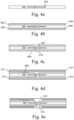
- Figs. 4 represents different stages of the manufacturing of a power module according to the present invention.
- the Fig. 4a represents a base layer 400 that is an electrically non-conductive and thermally conductive material.
- the base layer 400 is made of FR4.
- the base layer 400 is cut, for example by laser cut in order to form a cavity of the size of a power die 401.
- the power die 401 is then placed in the cavity.
- the base layer may be divided intwo or several layers separated by at least one higher thermally conductive layer 402 such as metal, like copper in order to increase heat spreading.
- isolation and conducting layers are laminated on the base layer formed at step S30.
- An example is given in Fig. 4b .
- the Fig. 4b represents the base layer 400 and the power die 401 on which a thin isolation layer 403 is laminated on the top of the base layer 400 and a thin isolation layer 406 is laminated on the bottom of the base layer 400.
- Electrically conducting layers 404 and 405, for example made of copper, are laminated also on the thin isolation layers 403 and 406. Insulation and conducting layers are laminated together in a single step.
- step S32 laser drilling and metallization are then made in order to connect the power die 401 to the conductor layer.
- An example is given in Fig. 4c .
- Laser drilling and metallization 407, 409 and 410 are then made in order to connect the power die 401 to the conductor layer.
- the power die contact to the conductor layers can cover completely the power die top and bottom surface, or partially, by using multiple via connections or other shapes.
- step S33 through hole vias are mechanically drilled and a further metallization is performed in order to connect the different conductor layers at different spots according to a layout.
- the conductor layers are etched, for example by a chemical or a mechanical process in order to obtain the desired layout like for example the one noted 408 on the thin conductor layer.
- step S35 if the number of conductor layers is not reached, the process returns to step S31. Otherwise, the process moves to step S36.
- Figs. 4 is an example wherein only two conductor layers are needed. According to this example, the process moves to step S31 and executes again the steps S31 to S34 one time.
- Additional thin isolation layers 411 and 412 and thick conductor layers 413, 414 are laminated on both sides of the sub-module as obtained at step S34.
- Laser drilling and metallization 415 and 416 are then made in order to connect the thin conductors layers 404 and 405 and the thick conductor layers 413 and 414.
- the connection can be made through multiple via connections or through other shapes like mettalized copper squares.
- the conductor layers are etched in order to obtain the desired layout on layers 413 and 414 and vias are formed. An example is given in Fig. 4f .
- Through hole vias 417 are made by drilling then metallizing. Also, board machining or drilling is performed in order to place capacitors 418 and magnetic materials.
- the conductor layers 413 and 414 are very thick, they can be pre-etched before lamination.
- machining and drilling are performed in order to obtain any desired module shape or drills on the module for any mechanical features sweeted to the final application. Machining and drilling can also be made in order to assemble later on additional components such as capacitors, magnetic materials for inductors or other.
- the two sub-modules are then assembled with thermally and electrically conductive materials in order to form the multilayer structure.
- step S38 external component soldering, attachment and magnetic material moulding is performed.
- capacitors are embedded within the two sub-modules of the power module as bus capacitors in order to smooth the bus voltage.
- Each capacitor is connected between the top layer of the top sub-module and the bottom layer of the bottom sub-module. Each capacitor is electrically connected after the assembling of the sub-modules. Each capacitor is placed in a verticle drill and is connected by soldering.
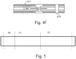
- Fig. 5 represents the different areas of a power module according to the present invention.
- the power module according to the present invention is decomposed into plural areas.
- gate drivers of the power dies are located.
- the decoupling or bus capacitors and power dies are located and in the area noted 53, an external inductor is located.
Landscapes
- Engineering & Computer Science (AREA)
- Microelectronics & Electronic Packaging (AREA)
- Inverter Devices (AREA)
- Cooling Or The Like Of Semiconductors Or Solid State Devices (AREA)
- Production Of Multi-Layered Print Wiring Board (AREA)
- Power Conversion In General (AREA)
- Manufacturing & Machinery (AREA)
- Physics & Mathematics (AREA)
- Geometry (AREA)
Claims (5)
- In mehrere Bereiche unterteiltes Leistungsmodul, umfassend mindestens zwei Leistungshalbleiter-Chips (401), bei demdas Leistungsmodul aus zwei Submodulen besteht, die mit thermisch und elektrisch leitenden Materialien zusammengesetzt sind, wobei jedes Submodul eine Mehrschichtstruktur aufweist,jedes Submodul mindestens einen Leistungshalbleiter-Chip (401) aufweist, wobei jedes Submodul mindestens einen Hohlraum mit darin eingesetztem Leistungshalbleiter-Chip (401) aufweist, wobei jedes Submodul aus Isolations- und Leiterschichten gebildet ist und jedes Submodul des Weiteren mindestens einen in die Mehrschichtstruktur eines Submoduls eingebetteten Kondensator (418) zur Entkopplung einer elektrischen Stromversorgung zu dem mindestens einen in der Mehrschichtstruktur eingebetteten Leistungshalbleiter-Chips (401) umfasst, und mindestens eine Treiberschaltung des mindestens einen Leistungshalbleiter-Chips (401) umfasst, die auf einer Oberfläche der Mehrschichtstruktur angeordnet oder ganz oder teilweise in die Mehrschichtstruktur eingebettet ist, wobei die mindestens eine Treiberschaltung in einem ersten Bereich (50) angeordnet ist, der mindestens eine Kondensator (418) in einem zweiten Bereich (51) angeordnet ist und ein externer Induktor in einem dritten Bereich (53) angeordnet ist, wobei nur ein Teil der Mehrschichtstruktur, die den mindestens einen Leistungshalbleiter-Chips (401) umfasst, durch eine flüssigkeitsgekühlte Sammelschiene (20a, 20b) gekühlt wird, und die elektrische Stromversorgung an den mindestens einen Leistungshalbleiter-Chip (401) über die flüssigkeitsgekühlte Sammelschiene (20a, 20b) erfolgt.
- Leistungsmodul nach Anspruch 1, bei dem jedes Submodul im Leistungsmodul des Weiteren ein magnetisches Material umfasst, das auf einer Oberfläche der Mehrschichtstruktur angeordnet oder ganz oder teilweise in die Mehrschichtstruktur eingebettet ist.
- Verfahren zur Herstellung eines in mehrere Bereiche unterteilten Leistungsmoduls nach Anspruch 1, umfassend mindestens zwei Leistungshalbleiter-Chips (401),wobei das Verfahren folgende Schritte umfasst:- Bilden mehrerer Submodule, wobei jedes Submodul aus Isolations- und Leiterschichten besteht und eine Mehrschichtstruktur aufweist,- Einbetten eines Leistungshalbleiter-Chips (401) in einen Hohlraum in jedem Submodul,wobei jedes Submodul mindestens ein Leistungshalbleiter-Chips (401) und mindestens einen Hohlraum aufweist,- Zusammensetzen der Submodule mit thermisch und elektrisch leitenden Materialien,- Einbetten mindestens eines Kondensators (418) in die Mehrschichtstruktur in jedem Submodul zur Entkopplung einer elektrischen Stromversorgung an den mindestens einen Leistungshalbleiter-Chip (401),- Aufbringen mindestens einer Treiberschaltung des mindestens einen Leistungshalbleiter-Chips (401) entweder auf einer Oberfläche der Mehrschichtstruktur oder ganz oder teilweise in die Mehrschichtstruktur eingebettet,wobei die mindestens eine Treiberschaltung in einem ersten Bereich (50) angeordnet ist, der mindestens eine Kondensator (418) in einem zweiten Bereich (51) angeordnet ist und ein externer Induktor in einem dritten Bereich (53) angeordnet ist, und nur ein Teil der den mindestens einen Leistungshalbleiter-Chips (401) umfassenden Mehrschichtstruktur durch eine flüssigkeitsgekühlte Sammelschiene (20a, 20b) gekühlt wird und die elektrische Stromversorgung an den mindestens einen Leistungshalbleiter-Chip (401) durch die flüssigkeitsgekühlte Sammelschiene (20a, 20b) erfolgt.
- Verfahren nach Anspruch 3, bei dem die Bildung jedes Submoduls durch Ausführen der folgenden Schritte nacheinander erfolgt:- Ausbilden mindestens eines Hohlraums in der Größe eines Leistungshalbleiter-Chips (401) in einer Basisschicht (400),- Anordnen des bzw. jedes Leistungshalbleiter-Chips (401) in einem Hohlraum,- Laminieren von isolierenden Schichten (403, 406) und leitenden Schichten (404, 405) auf die Basisschicht (400),- Bohren und Metallisieren (407, 409, 410) zur Verbindung des mindestens einen Leistungshalbleiter-Chips (401) mit den leitenden Schichten,- Ätzen der leitenden Schichten (404, 405) zum Erhalt eines Layouts,- Durchführen mindestens einer Laminierung von zusätzlichen dünnen Isolationsschichten (411, 412) und dicken Leiterschichten (413, 414) auf beiden Seiten der Basisschicht (400),- Bohren und Metallisieren (415, 416) zur Verbindung der Leiterschichten (404, 405) und der dicken Leiterschichten (413, 414),- Bilden von Durchgangslöchern (417).
- Verfahren nach einem der Ansprüche 3 bis 4, bei dem nach dem Zusammensetzen der Submodule der mindestens eine Kondensator (418) elektrisch zwischen einer oberen Schicht eines oberen Submoduls und einer unteren Schicht eines unteren Submoduls verbunden ist.
Priority Applications (5)
| Application Number | Priority Date | Filing Date | Title |
|---|---|---|---|
| EP16171013.2A EP3249686B1 (de) | 2016-05-24 | 2016-05-24 | Ein leistungsmodul |
| US16/090,734 US11152340B2 (en) | 2016-05-24 | 2017-04-05 | Power module having a multilayered structure with liquid cooled busbar and method for manufacturing same |
| JP2018535902A JP6742418B2 (ja) | 2016-05-24 | 2017-04-05 | パワーモジュール及びパワーモジュールの製造方法 |
| CN201780027211.6A CN109155298B (zh) | 2016-05-24 | 2017-04-05 | 功率模块和制造功率模块的方法 |
| PCT/JP2017/014885 WO2017203867A1 (en) | 2016-05-24 | 2017-04-05 | Power module and method for manufacturing power module |
Applications Claiming Priority (1)
| Application Number | Priority Date | Filing Date | Title |
|---|---|---|---|
| EP16171013.2A EP3249686B1 (de) | 2016-05-24 | 2016-05-24 | Ein leistungsmodul |
Publications (2)
| Publication Number | Publication Date |
|---|---|
| EP3249686A1 EP3249686A1 (de) | 2017-11-29 |
| EP3249686B1 true EP3249686B1 (de) | 2025-02-12 |
Family
ID=56081287
Family Applications (1)
| Application Number | Title | Priority Date | Filing Date |
|---|---|---|---|
| EP16171013.2A Active EP3249686B1 (de) | 2016-05-24 | 2016-05-24 | Ein leistungsmodul |
Country Status (5)
| Country | Link |
|---|---|
| US (1) | US11152340B2 (de) |
| EP (1) | EP3249686B1 (de) |
| JP (1) | JP6742418B2 (de) |
| CN (1) | CN109155298B (de) |
| WO (1) | WO2017203867A1 (de) |
Families Citing this family (5)
| Publication number | Priority date | Publication date | Assignee | Title |
|---|---|---|---|---|
| RU2726169C1 (ru) * | 2016-12-19 | 2020-07-09 | Абб Швайц Аг | Многофазная шина электропитания для передачи электроэнергии, способ ее изготовления и коммутационный шкаф, включающий в себя такую шину электропитания |
| EP3761492B1 (de) * | 2019-07-05 | 2023-01-04 | Infineon Technologies AG | Schutzbeschaltung und leistungshalbleitermodul mit der beschaltung |
| US11632860B2 (en) | 2019-10-25 | 2023-04-18 | Infineon Technologies Ag | Power electronic assembly and method of producing thereof |
| EP4030476A1 (de) * | 2021-01-15 | 2022-07-20 | Mitsubishi Electric R & D Centre Europe B.V. | Integrierter kühlflüssigkeitshohlraum in einer leiterplatte und verfahren zur herstellung davon |
| CN113937981A (zh) * | 2021-10-12 | 2022-01-14 | 臻驱科技(上海)有限公司 | 一种半导体模块衬底及电动车辆 |
Citations (1)
| Publication number | Priority date | Publication date | Assignee | Title |
|---|---|---|---|---|
| US20140319673A1 (en) * | 2011-11-07 | 2014-10-30 | Daikin Industries, Ltd. | Semiconductor device |
Family Cites Families (18)
| Publication number | Priority date | Publication date | Assignee | Title |
|---|---|---|---|---|
| US6305463B1 (en) * | 1996-02-22 | 2001-10-23 | Silicon Graphics, Inc. | Air or liquid cooled computer module cold plate |
| JP3721717B2 (ja) * | 1997-06-03 | 2005-11-30 | 株式会社明電舎 | 半導体素子の冷却構造 |
| EP1148772B1 (de) * | 2000-04-19 | 2009-12-23 | Thermal Form & Function Inc. | Kühlplatte mit Kühlrippen mit einem verdampfenden Kühlmittel |
| DE10108131A1 (de) * | 2001-02-21 | 2002-09-05 | Infineon Technologies Ag | Halbleiterschaltung und Schaltnetzteil |
| DE10139707A1 (de) * | 2001-08-11 | 2003-02-20 | Philips Corp Intellectual Pty | Leiterplatte |
| JP2004363568A (ja) | 2003-05-09 | 2004-12-24 | Matsushita Electric Ind Co Ltd | 回路素子内蔵モジュール |
| JP4292913B2 (ja) * | 2003-08-06 | 2009-07-08 | 株式会社デンソー | 半導体冷却ユニット |
| JP2006196853A (ja) * | 2004-12-13 | 2006-07-27 | Daikin Ind Ltd | ヒートポンプ装置 |
| JP2006303290A (ja) * | 2005-04-22 | 2006-11-02 | Mitsubishi Electric Corp | 半導体装置 |
| JP4935220B2 (ja) * | 2006-07-21 | 2012-05-23 | 三菱マテリアル株式会社 | パワーモジュール装置 |
| US7916480B2 (en) * | 2007-12-19 | 2011-03-29 | GM Global Technology Operations LLC | Busbar assembly with integrated cooling |
| JP5150246B2 (ja) * | 2007-12-28 | 2013-02-20 | 株式会社フジクラ | 多層プリント配線板及びその製造方法 |
| KR101093719B1 (ko) * | 2010-01-04 | 2011-12-19 | (주)웨이브닉스이에스피 | 금속기판을 이용한 고출력 소자의 패키지 모듈 구조 및 그 제조방법 |
| JP5218541B2 (ja) * | 2010-12-14 | 2013-06-26 | 株式会社デンソー | スイッチングモジュール |
| US9559047B2 (en) * | 2012-10-18 | 2017-01-31 | Infineon Technologies Austria Ag | Passive component as thermal capacitance and heat sink |
| JP2014086535A (ja) * | 2012-10-23 | 2014-05-12 | Denso Corp | 多層基板の放熱構造およびその製造方法 |
| EP3028547B1 (de) * | 2013-07-30 | 2019-12-11 | Harman Becker Automotive Systems GmbH | Elektronisches modul |
| US10064287B2 (en) * | 2014-11-05 | 2018-08-28 | Infineon Technologies Austria Ag | System and method of providing a semiconductor carrier and redistribution structure |
-
2016
- 2016-05-24 EP EP16171013.2A patent/EP3249686B1/de active Active
-
2017
- 2017-04-05 WO PCT/JP2017/014885 patent/WO2017203867A1/en not_active Ceased
- 2017-04-05 US US16/090,734 patent/US11152340B2/en active Active
- 2017-04-05 CN CN201780027211.6A patent/CN109155298B/zh active Active
- 2017-04-05 JP JP2018535902A patent/JP6742418B2/ja active Active
Patent Citations (1)
| Publication number | Priority date | Publication date | Assignee | Title |
|---|---|---|---|---|
| US20140319673A1 (en) * | 2011-11-07 | 2014-10-30 | Daikin Industries, Ltd. | Semiconductor device |
Also Published As
| Publication number | Publication date |
|---|---|
| CN109155298B (zh) | 2021-11-30 |
| EP3249686A1 (de) | 2017-11-29 |
| CN109155298A (zh) | 2019-01-04 |
| WO2017203867A1 (en) | 2017-11-30 |
| US20190123030A1 (en) | 2019-04-25 |
| JP2019504496A (ja) | 2019-02-14 |
| US11152340B2 (en) | 2021-10-19 |
| JP6742418B2 (ja) | 2020-08-19 |
Similar Documents
| Publication | Publication Date | Title |
|---|---|---|
| EP3249686B1 (de) | Ein leistungsmodul | |
| EP3249685B1 (de) | System mit mindestens einem strommodul mit mindestens einer strommatrize, die von einer flüssigkeitsgekühlten stromschiene gekühlt wird | |
| US10117334B2 (en) | Magnetic assembly | |
| US9620448B1 (en) | Power module | |
| US5641944A (en) | Power substrate with improved thermal characteristics | |
| KR20090005190A (ko) | 전자 컴포넌트 모듈 | |
| EP3584833B1 (de) | Leistungsmodul mit verbesserter ausrichtung | |
| EP3454350B1 (de) | Leistungshalbleitersysteme mit induktormodulen und verfahren zur herstellung von induktormodulen und leistungshalbleitersystemen mit induktormodulen | |
| US10734368B2 (en) | Parallelisable method for integrating power chips and power electronics | |
| CN110268520B (zh) | 用于集成功率芯片以及形成散热器的汇流条的方法 | |
| EP4016618B1 (de) | Verpackung für leistungsvorrichtungen | |
| US11515804B2 (en) | Electrical power circuit for an electrical power converter | |
| CN110383473B (zh) | 配备有形成散热器的汇流条的电力电子电路及集成方法 | |
| EP4274081A1 (de) | Modulare stromüberlagerungsvorrichtung und verfahren | |
| EP3319407B1 (de) | Modulare stromversorgung | |
| US10728999B2 (en) | Circuit boards and method to manufacture circuit boards | |
| US20250349640A1 (en) | Semiconductor Package and Array of Semiconductor Packages | |
| Popovic-Gerber et al. | An approach to building more compact power electronic converters | |
| TR2023015122A1 (tr) | Baski devre kartlarina elektroni̇k komponent gömülmesi̇ne yöneli̇k bi̇r üreti̇m yöntemi̇ | |
| JP2020502823A (ja) | パワーチップを集積するための方法およびパワーエレクトロニクスモジュール | |
| CN108135078A (zh) | 一种复合母排pcb板及其加工方法 |
Legal Events
| Date | Code | Title | Description |
|---|---|---|---|
| PUAI | Public reference made under article 153(3) epc to a published international application that has entered the european phase |
Free format text: ORIGINAL CODE: 0009012 |
|
| STAA | Information on the status of an ep patent application or granted ep patent |
Free format text: STATUS: THE APPLICATION HAS BEEN PUBLISHED |
|
| AK | Designated contracting states |
Kind code of ref document: A1 Designated state(s): AL AT BE BG CH CY CZ DE DK EE ES FI FR GB GR HR HU IE IS IT LI LT LU LV MC MK MT NL NO PL PT RO RS SE SI SK SM TR |
|
| AX | Request for extension of the european patent |
Extension state: BA ME |
|
| STAA | Information on the status of an ep patent application or granted ep patent |
Free format text: STATUS: REQUEST FOR EXAMINATION WAS MADE |
|
| 17P | Request for examination filed |
Effective date: 20180524 |
|
| RBV | Designated contracting states (corrected) |
Designated state(s): AL AT BE BG CH CY CZ DE DK EE ES FI FR GB GR HR HU IE IS IT LI LT LU LV MC MK MT NL NO PL PT RO RS SE SI SK SM TR |
|
| STAA | Information on the status of an ep patent application or granted ep patent |
Free format text: STATUS: EXAMINATION IS IN PROGRESS |
|
| 17Q | First examination report despatched |
Effective date: 20201207 |
|
| REG | Reference to a national code |
Ref country code: DE Ref legal event code: R079 Free format text: PREVIOUS MAIN CLASS: H01L0023485000 Ipc: H01L0021480000 Ref country code: DE Ref legal event code: R079 Ref document number: 602016091166 Country of ref document: DE Free format text: PREVIOUS MAIN CLASS: H01L0023485000 Ipc: H01L0021480000 |
|
| GRAP | Despatch of communication of intention to grant a patent |
Free format text: ORIGINAL CODE: EPIDOSNIGR1 |
|
| STAA | Information on the status of an ep patent application or granted ep patent |
Free format text: STATUS: GRANT OF PATENT IS INTENDED |
|
| RIC1 | Information provided on ipc code assigned before grant |
Ipc: H05K 3/46 20060101ALN20240711BHEP Ipc: H05K 1/02 20060101ALN20240711BHEP Ipc: H01L 23/31 20060101ALN20240711BHEP Ipc: H05K 1/18 20060101ALI20240711BHEP Ipc: H01L 25/16 20060101ALI20240711BHEP Ipc: H01L 23/64 20060101ALI20240711BHEP Ipc: H01L 23/473 20060101ALI20240711BHEP Ipc: H01L 23/29 20060101ALI20240711BHEP Ipc: H01L 21/48 20060101AFI20240711BHEP |
|
| INTG | Intention to grant announced |
Effective date: 20240722 |
|
| P01 | Opt-out of the competence of the unified patent court (upc) registered |
Free format text: CASE NUMBER: APP_49704/2024 Effective date: 20240902 |
|
| GRAS | Grant fee paid |
Free format text: ORIGINAL CODE: EPIDOSNIGR3 |
|
| GRAA | (expected) grant |
Free format text: ORIGINAL CODE: 0009210 |
|
| STAA | Information on the status of an ep patent application or granted ep patent |
Free format text: STATUS: THE PATENT HAS BEEN GRANTED |
|
| AK | Designated contracting states |
Kind code of ref document: B1 Designated state(s): AL AT BE BG CH CY CZ DE DK EE ES FI FR GB GR HR HU IE IS IT LI LT LU LV MC MK MT NL NO PL PT RO RS SE SI SK SM TR |
|
| REG | Reference to a national code |
Ref country code: GB Ref legal event code: FG4D |
|
| REG | Reference to a national code |
Ref country code: CH Ref legal event code: EP |
|
| REG | Reference to a national code |
Ref country code: DE Ref legal event code: R096 Ref document number: 602016091166 Country of ref document: DE |
|
| REG | Reference to a national code |
Ref country code: IE Ref legal event code: FG4D |
|
| REG | Reference to a national code |
Ref country code: NL Ref legal event code: MP Effective date: 20250212 |
|
| PG25 | Lapsed in a contracting state [announced via postgrant information from national office to epo] |
Ref country code: RS Free format text: LAPSE BECAUSE OF FAILURE TO SUBMIT A TRANSLATION OF THE DESCRIPTION OR TO PAY THE FEE WITHIN THE PRESCRIBED TIME-LIMIT Effective date: 20250512 |
|
| PG25 | Lapsed in a contracting state [announced via postgrant information from national office to epo] |
Ref country code: FI Free format text: LAPSE BECAUSE OF FAILURE TO SUBMIT A TRANSLATION OF THE DESCRIPTION OR TO PAY THE FEE WITHIN THE PRESCRIBED TIME-LIMIT Effective date: 20250212 |
|
| PG25 | Lapsed in a contracting state [announced via postgrant information from national office to epo] |
Ref country code: PL Free format text: LAPSE BECAUSE OF FAILURE TO SUBMIT A TRANSLATION OF THE DESCRIPTION OR TO PAY THE FEE WITHIN THE PRESCRIBED TIME-LIMIT Effective date: 20250212 |
|
| PGFP | Annual fee paid to national office [announced via postgrant information from national office to epo] |
Ref country code: DE Payment date: 20250521 Year of fee payment: 10 |
|
| PG25 | Lapsed in a contracting state [announced via postgrant information from national office to epo] |
Ref country code: ES Free format text: LAPSE BECAUSE OF FAILURE TO SUBMIT A TRANSLATION OF THE DESCRIPTION OR TO PAY THE FEE WITHIN THE PRESCRIBED TIME-LIMIT Effective date: 20250212 |
|
| PGFP | Annual fee paid to national office [announced via postgrant information from national office to epo] |
Ref country code: GB Payment date: 20250527 Year of fee payment: 10 |
|
| REG | Reference to a national code |
Ref country code: LT Ref legal event code: MG9D |
|
| PG25 | Lapsed in a contracting state [announced via postgrant information from national office to epo] |
Ref country code: IS Free format text: LAPSE BECAUSE OF FAILURE TO SUBMIT A TRANSLATION OF THE DESCRIPTION OR TO PAY THE FEE WITHIN THE PRESCRIBED TIME-LIMIT Effective date: 20250612 Ref country code: NO Free format text: LAPSE BECAUSE OF FAILURE TO SUBMIT A TRANSLATION OF THE DESCRIPTION OR TO PAY THE FEE WITHIN THE PRESCRIBED TIME-LIMIT Effective date: 20250512 |
|
| PG25 | Lapsed in a contracting state [announced via postgrant information from national office to epo] |
Ref country code: NL Free format text: LAPSE BECAUSE OF FAILURE TO SUBMIT A TRANSLATION OF THE DESCRIPTION OR TO PAY THE FEE WITHIN THE PRESCRIBED TIME-LIMIT Effective date: 20250212 |
|
| PG25 | Lapsed in a contracting state [announced via postgrant information from national office to epo] |
Ref country code: HR Free format text: LAPSE BECAUSE OF FAILURE TO SUBMIT A TRANSLATION OF THE DESCRIPTION OR TO PAY THE FEE WITHIN THE PRESCRIBED TIME-LIMIT Effective date: 20250212 |
|
| PG25 | Lapsed in a contracting state [announced via postgrant information from national office to epo] |
Ref country code: PT Free format text: LAPSE BECAUSE OF FAILURE TO SUBMIT A TRANSLATION OF THE DESCRIPTION OR TO PAY THE FEE WITHIN THE PRESCRIBED TIME-LIMIT Effective date: 20250612 Ref country code: LV Free format text: LAPSE BECAUSE OF FAILURE TO SUBMIT A TRANSLATION OF THE DESCRIPTION OR TO PAY THE FEE WITHIN THE PRESCRIBED TIME-LIMIT Effective date: 20250212 |
|
| PGFP | Annual fee paid to national office [announced via postgrant information from national office to epo] |
Ref country code: FR Payment date: 20250528 Year of fee payment: 10 |
|
| PG25 | Lapsed in a contracting state [announced via postgrant information from national office to epo] |
Ref country code: BG Free format text: LAPSE BECAUSE OF FAILURE TO SUBMIT A TRANSLATION OF THE DESCRIPTION OR TO PAY THE FEE WITHIN THE PRESCRIBED TIME-LIMIT Effective date: 20250212 Ref country code: GR Free format text: LAPSE BECAUSE OF FAILURE TO SUBMIT A TRANSLATION OF THE DESCRIPTION OR TO PAY THE FEE WITHIN THE PRESCRIBED TIME-LIMIT Effective date: 20250513 |
|
| REG | Reference to a national code |
Ref country code: AT Ref legal event code: MK05 Ref document number: 1766935 Country of ref document: AT Kind code of ref document: T Effective date: 20250212 |
|
| PG25 | Lapsed in a contracting state [announced via postgrant information from national office to epo] |
Ref country code: SE Free format text: LAPSE BECAUSE OF FAILURE TO SUBMIT A TRANSLATION OF THE DESCRIPTION OR TO PAY THE FEE WITHIN THE PRESCRIBED TIME-LIMIT Effective date: 20250212 |
|
| PG25 | Lapsed in a contracting state [announced via postgrant information from national office to epo] |
Ref country code: SM Free format text: LAPSE BECAUSE OF FAILURE TO SUBMIT A TRANSLATION OF THE DESCRIPTION OR TO PAY THE FEE WITHIN THE PRESCRIBED TIME-LIMIT Effective date: 20250212 |
|
| PG25 | Lapsed in a contracting state [announced via postgrant information from national office to epo] |
Ref country code: DK Free format text: LAPSE BECAUSE OF FAILURE TO SUBMIT A TRANSLATION OF THE DESCRIPTION OR TO PAY THE FEE WITHIN THE PRESCRIBED TIME-LIMIT Effective date: 20250212 |
|
| PG25 | Lapsed in a contracting state [announced via postgrant information from national office to epo] |
Ref country code: IT Free format text: LAPSE BECAUSE OF FAILURE TO SUBMIT A TRANSLATION OF THE DESCRIPTION OR TO PAY THE FEE WITHIN THE PRESCRIBED TIME-LIMIT Effective date: 20250212 |
|
| PG25 | Lapsed in a contracting state [announced via postgrant information from national office to epo] |
Ref country code: AT Free format text: LAPSE BECAUSE OF FAILURE TO SUBMIT A TRANSLATION OF THE DESCRIPTION OR TO PAY THE FEE WITHIN THE PRESCRIBED TIME-LIMIT Effective date: 20250212 |
|
| PG25 | Lapsed in a contracting state [announced via postgrant information from national office to epo] |
Ref country code: EE Free format text: LAPSE BECAUSE OF FAILURE TO SUBMIT A TRANSLATION OF THE DESCRIPTION OR TO PAY THE FEE WITHIN THE PRESCRIBED TIME-LIMIT Effective date: 20250212 Ref country code: CZ Free format text: LAPSE BECAUSE OF FAILURE TO SUBMIT A TRANSLATION OF THE DESCRIPTION OR TO PAY THE FEE WITHIN THE PRESCRIBED TIME-LIMIT Effective date: 20250212 |
|
| PG25 | Lapsed in a contracting state [announced via postgrant information from national office to epo] |
Ref country code: RO Free format text: LAPSE BECAUSE OF FAILURE TO SUBMIT A TRANSLATION OF THE DESCRIPTION OR TO PAY THE FEE WITHIN THE PRESCRIBED TIME-LIMIT Effective date: 20250212 |
|
| PG25 | Lapsed in a contracting state [announced via postgrant information from national office to epo] |
Ref country code: SK Free format text: LAPSE BECAUSE OF FAILURE TO SUBMIT A TRANSLATION OF THE DESCRIPTION OR TO PAY THE FEE WITHIN THE PRESCRIBED TIME-LIMIT Effective date: 20250212 |
|
| REG | Reference to a national code |
Ref country code: DE Ref legal event code: R097 Ref document number: 602016091166 Country of ref document: DE |
|
| REG | Reference to a national code |
Ref country code: DE Ref legal event code: R079 Ref document number: 602016091166 Country of ref document: DE Free format text: PREVIOUS MAIN CLASS: H01L0021480000 Ipc: H10W0076010000 |
|
| PLBE | No opposition filed within time limit |
Free format text: ORIGINAL CODE: 0009261 |
|
| STAA | Information on the status of an ep patent application or granted ep patent |
Free format text: STATUS: NO OPPOSITION FILED WITHIN TIME LIMIT |
|
| REG | Reference to a national code |
Ref country code: CH Ref legal event code: H13 Free format text: ST27 STATUS EVENT CODE: U-0-0-H10-H13 (AS PROVIDED BY THE NATIONAL OFFICE) Effective date: 20251223 |
|
| REG | Reference to a national code |
Ref country code: CH Ref legal event code: L10 Free format text: ST27 STATUS EVENT CODE: U-0-0-L10-L00 (AS PROVIDED BY THE NATIONAL OFFICE) Effective date: 20251224 |
|
| PG25 | Lapsed in a contracting state [announced via postgrant information from national office to epo] |
Ref country code: LU Free format text: LAPSE BECAUSE OF NON-PAYMENT OF DUE FEES Effective date: 20250524 |
|
| PG25 | Lapsed in a contracting state [announced via postgrant information from national office to epo] |
Ref country code: CH Free format text: LAPSE BECAUSE OF NON-PAYMENT OF DUE FEES Effective date: 20250531 |
|
| 26N | No opposition filed |
Effective date: 20251113 |
|
| REG | Reference to a national code |
Ref country code: BE Ref legal event code: MM Effective date: 20250531 |
|
| PG25 | Lapsed in a contracting state [announced via postgrant information from national office to epo] |
Ref country code: MC Free format text: LAPSE BECAUSE OF FAILURE TO SUBMIT A TRANSLATION OF THE DESCRIPTION OR TO PAY THE FEE WITHIN THE PRESCRIBED TIME-LIMIT Effective date: 20250212 |
|
| PG25 | Lapsed in a contracting state [announced via postgrant information from national office to epo] |
Ref country code: IE Free format text: LAPSE BECAUSE OF NON-PAYMENT OF DUE FEES Effective date: 20250524 |
|
| PG25 | Lapsed in a contracting state [announced via postgrant information from national office to epo] |
Ref country code: BE Free format text: LAPSE BECAUSE OF NON-PAYMENT OF DUE FEES Effective date: 20250531 |