EP3249073A1 - A method of cleaning a plasma processing device - Google Patents
A method of cleaning a plasma processing device Download PDFInfo
- Publication number
- EP3249073A1 EP3249073A1 EP17172574.0A EP17172574A EP3249073A1 EP 3249073 A1 EP3249073 A1 EP 3249073A1 EP 17172574 A EP17172574 A EP 17172574A EP 3249073 A1 EP3249073 A1 EP 3249073A1
- Authority
- EP
- European Patent Office
- Prior art keywords
- chamber
- cleaning
- radicals
- bias
- plasma source
- Prior art date
- Legal status (The legal status is an assumption and is not a legal conclusion. Google has not performed a legal analysis and makes no representation as to the accuracy of the status listed.)
- Pending
Links
Images


Classifications
-
- H—ELECTRICITY
- H01—ELECTRIC ELEMENTS
- H01J—ELECTRIC DISCHARGE TUBES OR DISCHARGE LAMPS
- H01J37/00—Discharge tubes with provision for introducing objects or material to be exposed to the discharge, e.g. for the purpose of examination or processing thereof
- H01J37/32—Gas-filled discharge tubes
- H01J37/32431—Constructional details of the reactor
- H01J37/32798—Further details of plasma apparatus not provided for in groups H01J37/3244 - H01J37/32788; special provisions for cleaning or maintenance of the apparatus
- H01J37/32853—Hygiene
- H01J37/32862—In situ cleaning of vessels and/or internal parts
-
- B—PERFORMING OPERATIONS; TRANSPORTING
- B08—CLEANING
- B08B—CLEANING IN GENERAL; PREVENTION OF FOULING IN GENERAL
- B08B7/00—Cleaning by methods not provided for in a single other subclass or a single group in this subclass
- B08B7/0035—Cleaning by methods not provided for in a single other subclass or a single group in this subclass by radiant energy, e.g. UV, laser, light beam or the like
-
- C—CHEMISTRY; METALLURGY
- C23—COATING METALLIC MATERIAL; COATING MATERIAL WITH METALLIC MATERIAL; CHEMICAL SURFACE TREATMENT; DIFFUSION TREATMENT OF METALLIC MATERIAL; COATING BY VACUUM EVAPORATION, BY SPUTTERING, BY ION IMPLANTATION OR BY CHEMICAL VAPOUR DEPOSITION, IN GENERAL; INHIBITING CORROSION OF METALLIC MATERIAL OR INCRUSTATION IN GENERAL
- C23C—COATING METALLIC MATERIAL; COATING MATERIAL WITH METALLIC MATERIAL; SURFACE TREATMENT OF METALLIC MATERIAL BY DIFFUSION INTO THE SURFACE, BY CHEMICAL CONVERSION OR SUBSTITUTION; COATING BY VACUUM EVAPORATION, BY SPUTTERING, BY ION IMPLANTATION OR BY CHEMICAL VAPOUR DEPOSITION, IN GENERAL
- C23C16/00—Chemical coating by decomposition of gaseous compounds, without leaving reaction products of surface material in the coating, i.e. chemical vapour deposition [CVD] processes
- C23C16/44—Chemical coating by decomposition of gaseous compounds, without leaving reaction products of surface material in the coating, i.e. chemical vapour deposition [CVD] processes characterised by the method of coating
- C23C16/4401—Means for minimising impurities, e.g. dust, moisture or residual gas, in the reaction chamber
- C23C16/4405—Cleaning of reactor or parts inside the reactor by using reactive gases
-
- C—CHEMISTRY; METALLURGY
- C23—COATING METALLIC MATERIAL; COATING MATERIAL WITH METALLIC MATERIAL; CHEMICAL SURFACE TREATMENT; DIFFUSION TREATMENT OF METALLIC MATERIAL; COATING BY VACUUM EVAPORATION, BY SPUTTERING, BY ION IMPLANTATION OR BY CHEMICAL VAPOUR DEPOSITION, IN GENERAL; INHIBITING CORROSION OF METALLIC MATERIAL OR INCRUSTATION IN GENERAL
- C23C—COATING METALLIC MATERIAL; COATING MATERIAL WITH METALLIC MATERIAL; SURFACE TREATMENT OF METALLIC MATERIAL BY DIFFUSION INTO THE SURFACE, BY CHEMICAL CONVERSION OR SUBSTITUTION; COATING BY VACUUM EVAPORATION, BY SPUTTERING, BY ION IMPLANTATION OR BY CHEMICAL VAPOUR DEPOSITION, IN GENERAL
- C23C16/00—Chemical coating by decomposition of gaseous compounds, without leaving reaction products of surface material in the coating, i.e. chemical vapour deposition [CVD] processes
- C23C16/44—Chemical coating by decomposition of gaseous compounds, without leaving reaction products of surface material in the coating, i.e. chemical vapour deposition [CVD] processes characterised by the method of coating
- C23C16/448—Chemical coating by decomposition of gaseous compounds, without leaving reaction products of surface material in the coating, i.e. chemical vapour deposition [CVD] processes characterised by the method of coating characterised by the method used for generating reactive gas streams, e.g. by evaporation or sublimation of precursor materials
- C23C16/452—Chemical coating by decomposition of gaseous compounds, without leaving reaction products of surface material in the coating, i.e. chemical vapour deposition [CVD] processes characterised by the method of coating characterised by the method used for generating reactive gas streams, e.g. by evaporation or sublimation of precursor materials by activating reactive gas streams before their introduction into the reaction chamber, e.g. by ionisation or addition of reactive species
-
- C—CHEMISTRY; METALLURGY
- C23—COATING METALLIC MATERIAL; COATING MATERIAL WITH METALLIC MATERIAL; CHEMICAL SURFACE TREATMENT; DIFFUSION TREATMENT OF METALLIC MATERIAL; COATING BY VACUUM EVAPORATION, BY SPUTTERING, BY ION IMPLANTATION OR BY CHEMICAL VAPOUR DEPOSITION, IN GENERAL; INHIBITING CORROSION OF METALLIC MATERIAL OR INCRUSTATION IN GENERAL
- C23C—COATING METALLIC MATERIAL; COATING MATERIAL WITH METALLIC MATERIAL; SURFACE TREATMENT OF METALLIC MATERIAL BY DIFFUSION INTO THE SURFACE, BY CHEMICAL CONVERSION OR SUBSTITUTION; COATING BY VACUUM EVAPORATION, BY SPUTTERING, BY ION IMPLANTATION OR BY CHEMICAL VAPOUR DEPOSITION, IN GENERAL
- C23C16/00—Chemical coating by decomposition of gaseous compounds, without leaving reaction products of surface material in the coating, i.e. chemical vapour deposition [CVD] processes
- C23C16/44—Chemical coating by decomposition of gaseous compounds, without leaving reaction products of surface material in the coating, i.e. chemical vapour deposition [CVD] processes characterised by the method of coating
- C23C16/52—Controlling or regulating the coating process
-
- H—ELECTRICITY
- H01—ELECTRIC ELEMENTS
- H01J—ELECTRIC DISCHARGE TUBES OR DISCHARGE LAMPS
- H01J37/00—Discharge tubes with provision for introducing objects or material to be exposed to the discharge, e.g. for the purpose of examination or processing thereof
- H01J37/32—Gas-filled discharge tubes
- H01J37/32009—Arrangements for generation of plasma specially adapted for examination or treatment of objects, e.g. plasma sources
- H01J37/32357—Generation remote from the workpiece, e.g. down-stream
-
- H—ELECTRICITY
- H01—ELECTRIC ELEMENTS
- H01J—ELECTRIC DISCHARGE TUBES OR DISCHARGE LAMPS
- H01J37/00—Discharge tubes with provision for introducing objects or material to be exposed to the discharge, e.g. for the purpose of examination or processing thereof
- H01J37/32—Gas-filled discharge tubes
- H01J37/32917—Plasma diagnostics
- H01J37/32935—Monitoring and controlling tubes by information coming from the object and/or discharge
- H01J37/32963—End-point detection
-
- H—ELECTRICITY
- H01—ELECTRIC ELEMENTS
- H01J—ELECTRIC DISCHARGE TUBES OR DISCHARGE LAMPS
- H01J2237/00—Discharge tubes exposing object to beam, e.g. for analysis treatment, etching, imaging
- H01J2237/32—Processing objects by plasma generation
- H01J2237/33—Processing objects by plasma generation characterised by the type of processing
- H01J2237/335—Cleaning
Definitions
- This invention relates to a method of cleaning a plasma processing device of the type having a remote plasma source for generating radicals which are used to perform the cleaning.
- the invention relates also to associated plasma processing devices.
- PECVD plasma enhanced chemical vapour deposition
- TSV back-end Through Silicon Via
- RPS remote plasma source
- Direct plasma cleaning involves the creation of a plasma in the process chamber itself for cleaning purposes.
- Direct plasma cleaning of silicon based dielectric films such as silicon dioxide and silicon nitride typically involves the detection of an optical end-point signal to determine when to stop the cleaning process. This is achieved by monitoring plasma intensity in the chamber by detecting suitable emissions, such as emission from ionised fluorine.
- US 7354778 discloses end-point detection in a direct plasma cleaning process in which a DC bias voltage of the plasma generator is monitored. Because the plasma generator is part of the direct plasma cleaning arrangement, the cleaning is performed using ionised process gases created in the chamber itself. Accordingly, the concentration of charged particles which would be expected to give rise to the DC bias voltage in the chamber is relatively high.
- An RPS cleaning system does not produce plasma inside the PECVD chamber, and so it is not possible to detect an optical end-point signal in the chamber, as there is no plasma in the chamber to produce an optical output. Additionally, there is no direct source of charged particles within the PECVD process chamber, which will be anticipated to dramatically reduce the concentration of charged particles available to produce a DC bias signal of the type detected in US 7354778 .
- an advantage associated with many RPS cleaning methodologies is that cleaning is performed primarily using radical species.
- the decoupling of the remote plasma source from the PECVD chamber in which cleaning takes place results in the majority of the charged species created by the cleaning plasma being prevented from entering the PECVD chamber.
- the consequent reduction of ion bombardment in the PECVD chamber has the advantage of resulting in less wear on chamber components. This has the consequential advantage of reducing the frequency of chamber interventions for maintenance purposes.
- US 6079426 , US 6543459 , and US2006/0090773 describe the detection of cleaning end-points for RPS devices.
- US 6079426 and US2006/0090773 disclose the detection of a cleaning end-point by monitoring chamber pressure.
- US 6543459 discloses a method of determining a cleaning end-point for a remote microwave plasma cleaning system in which capacitance changes are monitored.
- Another end-point detection technique uses infrared detection of a cleaning end-point. The measurements are made in the vacuum exhaust line downstream of the process chamber. This technique has been commercialised as the Process Sense (RTM) end-point sensor by MKS Instruments, Inc. of Methuen, MA 01844, USA.
- RTM Process Sense
- the present invention in at least some of its embodiments, provides an improved method of detecting a cleaning end-point in a RPS cleaning device which does not require the use of specialist, additional detectors such as optical or infra-red detectors.
- additional detectors such as optical or infra-red detectors.
- the invention is particularly suited to the cleaning of PECVD devices, the invention can be used in conjunction with the cleaning of other processing devices as well.
- a method of cleaning a chamber of a plasma processing device with radicals comprising the steps of:
- radicals' is intended to refer to uncharged reactive species having one or more unpaired electrons.
- the radicals may be atomic or molecular.
- a measurable and useful DC bias signal can be developed on a component of the process chamber even though charged particles are not produced in the process chamber during the cleaning process. Ions and electrons are produced during cleaning in the remote plasma source. However, these species are short-lived and the majority of them do not reach the process chamber. In fact, it is expected that substantially all (95% or more) of the electrons and ions created in the remote plasma source do not reach the process chamber. Accordingly, it is very surprising that a measurable and useful DC bias signal can be developed on a component of the process chamber.
- the DC bias signal is easy to measure and does not require the use of specialist, additional detectors such as optical or infra-red detectors. An additional benefit is that detection takes place directly in the process chamber in which the cleaning takes place.
- the component may be a component of a gas inlet system.
- the component may act as a conduit for radicals produced in the remote plasma source.
- the component is a showerhead.
- a showerhead is a gas supply element having a plurality of perforations or other apertures. The perforations or other apertures allow gas to be introduced evenly into the process chamber 12.
- the showerhead comprises a first plate having a gas inlet and a second plate which carries the perforations or other apertures. The first and second plates are spaced apart to define a cavity.
- the component may be a substrate support.
- the substrate support may be a platen.
- the component may be an electrically isolated portion of a wall of the chamber, or a pumping gallery.
- a pumping gallery may be a conduit for exhausting gases which is defined by one or more walls of the chamber.
- the component is formed from an electrically conductive material such as a metal.
- the metal may be aluminium.
- the plasma processing device may be a PECVD device.
- the end-point may be determined by detecting that the DC bias has attained a steady-state.
- the cleaning may be performed using F radicals.
- the plasma created within the remote plasma source may use NF 3 as a precursor.
- the chamber may be cleaned after one or more dielectric films have been deposited in the chamber.
- the dielectric films may be films of a silicon containing dielectric material.
- the silicon containing dielectric material may be silicon dioxide or silicon nitride.
- the cleaning may be performed after plasma processing of a semiconductor substrate.
- the semiconductor substrate may be a silicon substrate.
- the semiconductor substrate may be a semiconductor wafer, such as a silicon wafer.
- the cleaning may be performed after an isolation or passivation plasma processing step.
- the cleaning may be performed after a TSV, via reveal or interposer manufacture plasma processing step.
- a plasma processing device comprising; a chamber; a remote plasma source which is configured to, in use, create a plasma comprising radicals and ions; a connector which separates the remote plasma source from the chamber and which allows radicals to enter the chamber while prevent the majority of the ions created in the remote plasma source from entering chamber so that the chamber can undergo cleaning by radicals; a detector for detecting a DC bias developed on a component of the chamber during cleaning; and a controller which is configured to use the detected DC bias to determine an end-point of the cleaning and, on determination of the end-point, to stop the cleaning.
- the connector may be electrically insulating.
- the connector may be formed from a dielectric material such as a ceramic.
- the connector may comprise a plurality of gas conducting bores.
- the gas conducting bores may each have a diameter of less than 10mm, preferably less than 5mm. In this way, plasma generated in the remote plasma source is substantially prevented from reaching the chamber.
- the connector may comprise a plug having the plurality of gas conducting bores formed therethrough.
- the device may be a PECVD device.
- the remote plasma source may be an inductively coupled plasma (ICP) source or any other suitable plasma source.
- ICP inductively coupled plasma
- FIG. 1 shows a PECVD device, depicted generally at 10, of the invention.
- the PECVD device 10 is of the type comprising a process chamber 12 and a remote plasma source 14 which is positioned remotely from the process chamber 12.
- the remote plasma source 14 is connected to the process chamber 12 by an isolator 16 which has a gas feed through.
- a gas inlet system is provided which comprises a suitable gas supply 18 system 16 for supplying one or more process gases to the process chamber 12.
- the gas inlet system further comprises a showerhead 20 which constitutes a top portion of the process chamber 12.
- the showerhead is a gas supply element having a plurality of perforations or other apertures which allow gas to be introduced evenly into the main body portion of the process chamber 12.
- Gases entering the showerhead 20 from the gas supply system form a gas reservoir in the interior volume of the showerhead 20 before passing through the perforations or other apertures into the main body of the process chamber 12.
- the showerhead is formed from electrically conductive material such as aluminium or another suitable metal.
- an RF electrical signal is applied to the showerhead 20 by an RF generator 30.
- the showerhead 20 is electrically isolated from the remainder of the process chamber 12 by a ceramic isolator 22.
- a platen 24 is located within the process chamber 12.
- a wafer or other workpiece to be processed is mounted on the platen 24.
- the device 10 further comprises an exhaust foreline 26 which is in connection with a suitable pump (not shown).
- a FTIR monitoring system 28 is provided for monitoring cleaning by-products passing through the foreline 26.
- the FTIR monitoring system 28 has been included in the device 10 shown in Figure 1 in order to provide comparative data to assess the performance of the invention.
- the FTIR monitoring system 28 does not form part of the present inventive concept and is not an essential element of the present invention.
- the process chamber 12 is earthed at a point 32 and the platen 24 is earthed at a point 34.
- the device 10 further comprises a suitable detector (not shown) for measuring a DC bias developed on the showerhead 20 during cleaning and a controller (not shown) for determining the end-point of a cleaning operation based on the measured DC bias. On determination of the end-point, the controller ends the cleaning operation.
- the controller can be a computer or another microprocessor based control device as is well known in the art. Typically, the controller also controls other operations of the PECVD device.
- the remote plasma source 14 comprises a suitable plasma generation device to initiate and sustain a plasma in a gaseous atmosphere supplied by the remote plasma source gas supply system 36.
- the remote plasma source may be an inductively coupled plasma (ICP) source powered by an RF electrical supply 38.
- ICP inductively coupled plasma
- Other forms of plasma generator might be contemplated instead.
- the plasma created in the remote plasma source 14 comprises a mixture of energetic, excited particles including ions, electrons and neutral radical species.
- the cleaning of the process chamber 12 is primarily performed with radicals which are introduced into the process chamber 12 via the ceramic isolator 16.
- the ceramic isolator 16 electrically isolates the remote plasma source 14 from the showerhead 20 on the process chamber 12.
- the isolator 16 comprises a series of relatively small diameter holes formed in the ceramic such as by drilling.
- a series of holes of approximately 3mm diameter are formed in the isolator to prevent the plasma generated in the remote plasma source 14 from reaching the back face of the showerhead 20. Radicals generated by the plasma produced in the remote plasma source 14 pass through the series of holes in the isolator 16 and enter the process chamber 12 through the showerhead 22. These radicals are used to clean the surfaces of the process chamber 12. For example, dielectric film deposited during the processing that takes place in the process chamber 12 is removed from the chamber surfaces by the radical cleaning. Because the process chamber 12 is substantially decoupled from the cleaning plasma in the remote plasma source 14, there is a substantial reduction in ion bombardment which results in less wear on the chamber components and consequently reduces the frequency of chamber intervention for maintenance purposes.
- a DC bias is developed on certain components of the chamber 12 during the cleaning process.
- the DC bias has been observed to change as the dielectric film in the chamber is cleaned. It has been realised that the DC bias can indicate when the cleaning process is complete. In particular, a plateau or other steady-state condition in the DC bias can be indicative that the cleaning process is complete. It is very surprising that the DC bias in the chamber is observable and that it can be useful in determining a cleaning end-point. Without wishing to be bound by any particular theory or conjecture, it is believed that the DC bias observed on components in the chamber is due to the presence of ions and electrons reaching the components and inducing a small positive or negative charge on the component.
- a PECVD device as shown in Figure 1 was used to deposit a range of dielectric films onto silicon wafers. After deposition of a desired type of dielectric film, cleaning of the process chamber was performed. The cleaning process was monitored by detecting DC bias induced on the showerhead and FTIR signal obtained from cleaning by-products in the foreline.
- a range of films were deposited including silicon oxide, silicon nitrides and film stacks comprising layers of silicon nitride and silicon oxide. Silicon oxide films were deposited using different methodologies, namely known techniques using tetraethyl orthosilicate (TEOS) and silane as precursors. Films were produced with thicknesses ranging from 100nm to 3.2 micron using deposition temperatures from 125°C to 350°C.
- TEOS tetraethyl orthosilicate
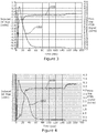
- Figures 2 , 3 and 4 show induced DC bias signal 100 and FTIR signal 102 obtained during cleaning after deposition of a number of films. More particularly, Figure 2 relates to cleaning after deposition of a 0.6 micron silicon dioxide film at 125°C using the TEOS method with an aluminium showerhead. Both DC bias 100 and FTIR 102 signals plateau at around 120 second, indicating that the chamber is clean. Figure 3 relates to cleaning after deposition of a 0.2 micron silicon nitride film deposited at 125°C with an aluminium showerhead. DC bias 100 and FTIR 102 signals both plateau at around 80 seconds, indicating the process chamber is clean.
- the steady-state DC bias attained is more negative in comparison to the silicon dioxide film deposited using the TEOS method ( Figure 2 ).
- Figure 4 relates to cleaning after deposition of a dielectric film stack at 125°C using an anodised aluminium showerhead.
- the stack comprises layers of a 1.05 micron thick silicon nitride film and 0.6 micron thick layers of silicon dioxide deposited using the TEOS method.
- DC bias 100 and FTIR 102 signals both plateau at around 110 seconds, indicating the process chamber is clean.
- the time to cleaning end-points obtained are not directly proportional to the film thickness. This is not unexpected, because other factors are believed to play a part in determining the time to end-point. Relevant factors include the type of film and the process used to deposit the film. Different processes and film types deposit differently in the chamber, resulting in a non-uniform coating to be removed. For example, one silicon nitride process may deposit a thicker film at the edge of the showerhead compared to another silicon nitride deposition process. This would result in a different time to end-point. Clean process development has shown that the etch rate of the deposited material is slightly lower at the edge of the showerhead compared to the centre.
- the DC bias signals associated with the different films differ from one another in terms of absolute values and general shapes. This can be attributed to different film types having different dielectric properties. It is believed that this changes the overall chamber impedance, resulting is small differences in the induced DC bias. In addition to this, it is believed that different processes deposit dielectric films in different areas of the chamber, resulting in small changes to the overall chamber impedance. It is believed that subtle changes in chamber impedance are responsible for small differences in the induced DC bias on the showerhead.
- the showerhead is a particularly convenient component for monitoring induced DC bias in the process chamber, other components of the process chamber on which DC bias can be induced might be monitored. For example, DC bias might be monitored on other components on a gas inlet system, an electrically isolated portion of a wall of the chamber, the platen, or the pumping gallery of the chamber.
Landscapes
- Chemical & Material Sciences (AREA)
- Engineering & Computer Science (AREA)
- Physics & Mathematics (AREA)
- Analytical Chemistry (AREA)
- Plasma & Fusion (AREA)
- Materials Engineering (AREA)
- Metallurgy (AREA)
- Organic Chemistry (AREA)
- Mechanical Engineering (AREA)
- Chemical Kinetics & Catalysis (AREA)
- General Chemical & Material Sciences (AREA)
- Health & Medical Sciences (AREA)
- Epidemiology (AREA)
- Public Health (AREA)
- Optics & Photonics (AREA)
- Chemical Vapour Deposition (AREA)
- Drying Of Semiconductors (AREA)
- Plasma Technology (AREA)
- Physical Vapour Deposition (AREA)
Applications Claiming Priority (1)
| Application Number | Priority Date | Filing Date | Title |
|---|---|---|---|
| GBGB1609119.1A GB201609119D0 (en) | 2016-05-24 | 2016-05-24 | A method of cleaning a plasma processing module |
Publications (1)
| Publication Number | Publication Date |
|---|---|
| EP3249073A1 true EP3249073A1 (en) | 2017-11-29 |
Family
ID=56369881
Family Applications (1)
| Application Number | Title | Priority Date | Filing Date |
|---|---|---|---|
| EP17172574.0A Pending EP3249073A1 (en) | 2016-05-24 | 2017-05-23 | A method of cleaning a plasma processing device |
Country Status (7)
| Country | Link |
|---|---|
| US (1) | US10309014B2 (zh) |
| EP (1) | EP3249073A1 (zh) |
| JP (1) | JP7011403B2 (zh) |
| KR (1) | KR102185805B1 (zh) |
| CN (1) | CN107424898B (zh) |
| GB (1) | GB201609119D0 (zh) |
| TW (1) | TWI795358B (zh) |
Families Citing this family (36)
| Publication number | Priority date | Publication date | Assignee | Title |
|---|---|---|---|---|
| US9132436B2 (en) | 2012-09-21 | 2015-09-15 | Applied Materials, Inc. | Chemical control features in wafer process equipment |
| US10256079B2 (en) | 2013-02-08 | 2019-04-09 | Applied Materials, Inc. | Semiconductor processing systems having multiple plasma configurations |
| US11637002B2 (en) | 2014-11-26 | 2023-04-25 | Applied Materials, Inc. | Methods and systems to enhance process uniformity |
| US20160225652A1 (en) | 2015-02-03 | 2016-08-04 | Applied Materials, Inc. | Low temperature chuck for plasma processing systems |
| US9741593B2 (en) | 2015-08-06 | 2017-08-22 | Applied Materials, Inc. | Thermal management systems and methods for wafer processing systems |
| US10504700B2 (en) | 2015-08-27 | 2019-12-10 | Applied Materials, Inc. | Plasma etching systems and methods with secondary plasma injection |
| US10504754B2 (en) | 2016-05-19 | 2019-12-10 | Applied Materials, Inc. | Systems and methods for improved semiconductor etching and component protection |
| US9865484B1 (en) | 2016-06-29 | 2018-01-09 | Applied Materials, Inc. | Selective etch using material modification and RF pulsing |
| US10546729B2 (en) | 2016-10-04 | 2020-01-28 | Applied Materials, Inc. | Dual-channel showerhead with improved profile |
| CN108300978B (zh) * | 2017-01-12 | 2020-10-09 | 和舰科技(苏州)有限公司 | 一种侦测气相沉积机台清理结束时间点的装置和方法 |
| US10431429B2 (en) | 2017-02-03 | 2019-10-01 | Applied Materials, Inc. | Systems and methods for radial and azimuthal control of plasma uniformity |
| US10943834B2 (en) | 2017-03-13 | 2021-03-09 | Applied Materials, Inc. | Replacement contact process |
| US11276590B2 (en) | 2017-05-17 | 2022-03-15 | Applied Materials, Inc. | Multi-zone semiconductor substrate supports |
| US11276559B2 (en) | 2017-05-17 | 2022-03-15 | Applied Materials, Inc. | Semiconductor processing chamber for multiple precursor flow |
| US10297458B2 (en) | 2017-08-07 | 2019-05-21 | Applied Materials, Inc. | Process window widening using coated parts in plasma etch processes |
| US10903054B2 (en) | 2017-12-19 | 2021-01-26 | Applied Materials, Inc. | Multi-zone gas distribution systems and methods |
| US11328909B2 (en) | 2017-12-22 | 2022-05-10 | Applied Materials, Inc. | Chamber conditioning and removal processes |
| US10854426B2 (en) | 2018-01-08 | 2020-12-01 | Applied Materials, Inc. | Metal recess for semiconductor structures |
| US10964512B2 (en) | 2018-02-15 | 2021-03-30 | Applied Materials, Inc. | Semiconductor processing chamber multistage mixing apparatus and methods |
| US10319600B1 (en) | 2018-03-12 | 2019-06-11 | Applied Materials, Inc. | Thermal silicon etch |
| US10886137B2 (en) | 2018-04-30 | 2021-01-05 | Applied Materials, Inc. | Selective nitride removal |
| TWI838387B (zh) * | 2018-07-09 | 2024-04-11 | 美商蘭姆研究公司 | 功率供應系統、基板處理系統、及供應功率的方法 |
| US11049755B2 (en) | 2018-09-14 | 2021-06-29 | Applied Materials, Inc. | Semiconductor substrate supports with embedded RF shield |
| US10892198B2 (en) | 2018-09-14 | 2021-01-12 | Applied Materials, Inc. | Systems and methods for improved performance in semiconductor processing |
| US11062887B2 (en) | 2018-09-17 | 2021-07-13 | Applied Materials, Inc. | High temperature RF heater pedestals |
| US11417534B2 (en) | 2018-09-21 | 2022-08-16 | Applied Materials, Inc. | Selective material removal |
| US11682560B2 (en) | 2018-10-11 | 2023-06-20 | Applied Materials, Inc. | Systems and methods for hafnium-containing film removal |
| US11121002B2 (en) | 2018-10-24 | 2021-09-14 | Applied Materials, Inc. | Systems and methods for etching metals and metal derivatives |
| US11437242B2 (en) | 2018-11-27 | 2022-09-06 | Applied Materials, Inc. | Selective removal of silicon-containing materials |
| US11721527B2 (en) * | 2019-01-07 | 2023-08-08 | Applied Materials, Inc. | Processing chamber mixing systems |
| US10920319B2 (en) | 2019-01-11 | 2021-02-16 | Applied Materials, Inc. | Ceramic showerheads with conductive electrodes |
| US20200266037A1 (en) * | 2019-02-14 | 2020-08-20 | Advanced Energy Industries, Inc. | Maintenance for remote plasma sources |
| US11264219B2 (en) * | 2019-04-17 | 2022-03-01 | Samsung Electronics Co., Ltd. | Radical monitoring apparatus and plasma apparatus including the monitoring apparatus |
| TWI748741B (zh) * | 2020-11-11 | 2021-12-01 | 暉盛科技股份有限公司 | 電漿晶圓清潔機及使用其清潔晶圓的方法 |
| KR20220093499A (ko) * | 2020-12-28 | 2022-07-05 | 에스케이스페셜티 주식회사 | F3no 가스를 이용한 반도체 및 디스플레이 화학기상 증착 챔버의 건식 세정 방법 |
| WO2024107561A1 (en) * | 2022-11-16 | 2024-05-23 | Mks Instruments, Inc. | Radical sensing for process tool diagnostics |
Citations (5)
| Publication number | Priority date | Publication date | Assignee | Title |
|---|---|---|---|---|
| JPH1022280A (ja) * | 1996-07-08 | 1998-01-23 | Hitachi Ltd | プラズマcvd装置およびそのクリーニング方法 |
| US5830310A (en) * | 1995-01-13 | 1998-11-03 | Anelva Corporation | Apparatus and method for detecting end point of post treatment |
| US6297165B1 (en) * | 1998-06-26 | 2001-10-02 | Matsushita Electric Industrial Co., Ltd. | Etching and cleaning methods |
| US6543459B1 (en) * | 2000-04-07 | 2003-04-08 | Koninklijke Philips Electronics N.V. | Method of determining an end point for a remote microwave plasma cleaning system |
| US20090035945A1 (en) * | 2007-07-31 | 2009-02-05 | Renesas Technology Corp. | Manufacturing method of semiconductor integrated circuit device |
Family Cites Families (10)
| Publication number | Priority date | Publication date | Assignee | Title |
|---|---|---|---|---|
| US6079426A (en) * | 1997-07-02 | 2000-06-27 | Applied Materials, Inc. | Method and apparatus for determining the endpoint in a plasma cleaning process |
| JP2002151417A (ja) | 2000-11-08 | 2002-05-24 | Hitachi Ltd | プラズマcvd装置 |
| JP2002151475A (ja) | 2000-11-14 | 2002-05-24 | Toshiba Corp | 薄膜処理モニタリング方法と薄膜処理装置 |
| DE10241590A1 (de) | 2002-09-05 | 2004-03-18 | Infineon Technologies Ag | Verfahren zur Bestimmung des Endpunktes beim Reinigungsätzen |
| JP2005033173A (ja) * | 2003-06-16 | 2005-02-03 | Renesas Technology Corp | 半導体集積回路装置の製造方法 |
| KR100710923B1 (ko) * | 2004-06-02 | 2007-04-23 | 동경 엘렉트론 주식회사 | 플라즈마 처리장치 및 임피던스 조정방법 |
| US20060090773A1 (en) * | 2004-11-04 | 2006-05-04 | Applied Materials, Inc. | Sulfur hexafluoride remote plasma source clean |
| TWI355038B (en) * | 2006-10-04 | 2011-12-21 | Macronix Int Co Ltd | Method of monitoring plasma process tool, protecti |
| KR20100069392A (ko) * | 2008-12-16 | 2010-06-24 | 삼성전자주식회사 | 증착, 식각 혹은 클리닝 공정에서 증착, 식각 혹은 클리닝 종료 시점을 결정하기 위하여 수정 결정 미소저울을 이용하는 반도체 소자의 제조장치 및 이를 이용한 제조방법 |
| US8591659B1 (en) * | 2009-01-16 | 2013-11-26 | Novellus Systems, Inc. | Plasma clean method for deposition chamber |
-
2016
- 2016-05-24 GB GBGB1609119.1A patent/GB201609119D0/en not_active Ceased
-
2017
- 2017-05-09 US US15/590,063 patent/US10309014B2/en active Active
- 2017-05-09 TW TW106115328A patent/TWI795358B/zh active
- 2017-05-19 CN CN201710358043.0A patent/CN107424898B/zh active Active
- 2017-05-23 JP JP2017101388A patent/JP7011403B2/ja active Active
- 2017-05-23 EP EP17172574.0A patent/EP3249073A1/en active Pending
- 2017-05-23 KR KR1020170063644A patent/KR102185805B1/ko active IP Right Grant
Patent Citations (5)
| Publication number | Priority date | Publication date | Assignee | Title |
|---|---|---|---|---|
| US5830310A (en) * | 1995-01-13 | 1998-11-03 | Anelva Corporation | Apparatus and method for detecting end point of post treatment |
| JPH1022280A (ja) * | 1996-07-08 | 1998-01-23 | Hitachi Ltd | プラズマcvd装置およびそのクリーニング方法 |
| US6297165B1 (en) * | 1998-06-26 | 2001-10-02 | Matsushita Electric Industrial Co., Ltd. | Etching and cleaning methods |
| US6543459B1 (en) * | 2000-04-07 | 2003-04-08 | Koninklijke Philips Electronics N.V. | Method of determining an end point for a remote microwave plasma cleaning system |
| US20090035945A1 (en) * | 2007-07-31 | 2009-02-05 | Renesas Technology Corp. | Manufacturing method of semiconductor integrated circuit device |
Also Published As
| Publication number | Publication date |
|---|---|
| US10309014B2 (en) | 2019-06-04 |
| US20170342556A1 (en) | 2017-11-30 |
| TW201805079A (zh) | 2018-02-16 |
| GB201609119D0 (en) | 2016-07-06 |
| JP2017212445A (ja) | 2017-11-30 |
| CN107424898B (zh) | 2021-03-19 |
| KR20170132685A (ko) | 2017-12-04 |
| CN107424898A (zh) | 2017-12-01 |
| KR102185805B1 (ko) | 2020-12-02 |
| TWI795358B (zh) | 2023-03-11 |
| JP7011403B2 (ja) | 2022-01-26 |
Similar Documents
| Publication | Publication Date | Title |
|---|---|---|
| EP3249073A1 (en) | A method of cleaning a plasma processing device | |
| JP5709912B2 (ja) | プラズマ処理システムにおけるクリーニングまたはコンディショニングプロセスのエンドポイント決定方法及び装置 | |
| TWI591742B (zh) | 藉由監視微量氣體濃度以偵測晶圓電漿處理中之發弧現象 | |
| KR20180106816A (ko) | 플라스마 처리 장치 및 플라스마 처리 방법 | |
| KR101429291B1 (ko) | 반도체 집적회로장치의 제조방법 | |
| US10267728B2 (en) | Systems and methods for detecting oxygen in-situ in a substrate area of a substrate processing system | |
| EP0308516A1 (en) | Method of determining end point of cleaning in an apparatus for manufacturing semiconductor devices | |
| WO2002091453A9 (en) | High pressure wafer-less auto clean for etch applications | |
| KR101015730B1 (ko) | 종료점을 사용한 에치특성을 구하는 장치 및 방법 | |
| US20190043700A1 (en) | Effluent impedance based endpoint detection | |
| TWI791524B (zh) | 用於製造電子裝置的設備、用於製造半導體裝置的設備以及估計在半導體處理腔室中的氣體濃度之方法 | |
| Hebner | CF, CF2, and SiF densities in inductively driven discharges containing C2F6, C4F8, and CHF3 | |
| KR20080018810A (ko) | 세정 공정의 종말점을 검출하는 방법 | |
| JP2006294658A (ja) | プラズマ処理装置 | |
| US20060228815A1 (en) | Inductively coupled plasma chamber attachable to a processing chamber for analysis of process gases | |
| CN115176328A (zh) | 用于等离子体腔室条件监测的电容感测数据集成 | |
| CN107546141B (zh) | 监测等离子体工艺制程的装置和方法 | |
| JP4845816B2 (ja) | プラズマ処理装置 | |
| US20210307151A1 (en) | Air Leak Detection In Plasma Processing Apparatus With Separation Grid | |
| Han et al. | Modified PCA algorithm for the end point monitoring of the small open area plasma etching process using the whole optical emission spectra | |
| JP2005019763A (ja) | ドライエッチング装置 | |
| JPH05175165A (ja) | プラズマ装置 | |
| KR20120010073A (ko) | 플라즈마처리장치 및 플라즈마처리방법 | |
| CN107644811A (zh) | 博世工艺的刻蚀终点监测方法以及博世刻蚀方法 | |
| JP2008270587A (ja) | プラズマ処理終点検出方法 |
Legal Events
| Date | Code | Title | Description |
|---|---|---|---|
| PUAI | Public reference made under article 153(3) epc to a published international application that has entered the european phase |
Free format text: ORIGINAL CODE: 0009012 |
|
| STAA | Information on the status of an ep patent application or granted ep patent |
Free format text: STATUS: THE APPLICATION HAS BEEN PUBLISHED |
|
| AK | Designated contracting states |
Kind code of ref document: A1 Designated state(s): AL AT BE BG CH CY CZ DE DK EE ES FI FR GB GR HR HU IE IS IT LI LT LU LV MC MK MT NL NO PL PT RO RS SE SI SK SM TR |
|
| AX | Request for extension of the european patent |
Extension state: BA ME |
|
| STAA | Information on the status of an ep patent application or granted ep patent |
Free format text: STATUS: REQUEST FOR EXAMINATION WAS MADE |
|
| 17P | Request for examination filed |
Effective date: 20180529 |
|
| RBV | Designated contracting states (corrected) |
Designated state(s): AL AT BE BG CH CY CZ DE DK EE ES FI FR GB GR HR HU IE IS IT LI LT LU LV MC MK MT NL NO PL PT RO RS SE SI SK SM TR |
|
| STAA | Information on the status of an ep patent application or granted ep patent |
Free format text: STATUS: EXAMINATION IS IN PROGRESS |
|
| STAA | Information on the status of an ep patent application or granted ep patent |
Free format text: STATUS: EXAMINATION IS IN PROGRESS |
|
| 17Q | First examination report despatched |
Effective date: 20211022 |
|
| P01 | Opt-out of the competence of the unified patent court (upc) registered |
Effective date: 20230527 |