EP3244518A1 - Strombegrenzte leistungswandlerschaltungen und verfahren - Google Patents
Strombegrenzte leistungswandlerschaltungen und verfahren Download PDFInfo
- Publication number
- EP3244518A1 EP3244518A1 EP17168548.0A EP17168548A EP3244518A1 EP 3244518 A1 EP3244518 A1 EP 3244518A1 EP 17168548 A EP17168548 A EP 17168548A EP 3244518 A1 EP3244518 A1 EP 3244518A1
- Authority
- EP
- European Patent Office
- Prior art keywords
- circuit
- current
- power train
- current limit
- power converter
- Prior art date
- Legal status (The legal status is an assumption and is not a legal conclusion. Google has not performed a legal analysis and makes no representation as to the accuracy of the status listed.)
- Ceased
Links
Images


Classifications
-
- H—ELECTRICITY
- H02—GENERATION; CONVERSION OR DISTRIBUTION OF ELECTRIC POWER
- H02M—APPARATUS FOR CONVERSION BETWEEN AC AND AC, BETWEEN AC AND DC, OR BETWEEN DC AND DC, AND FOR USE WITH MAINS OR SIMILAR POWER SUPPLY SYSTEMS; CONVERSION OF DC OR AC INPUT POWER INTO SURGE OUTPUT POWER; CONTROL OR REGULATION THEREOF
- H02M1/00—Details of apparatus for conversion
- H02M1/32—Means for protecting converters other than automatic disconnection
-
- H—ELECTRICITY
- H02—GENERATION; CONVERSION OR DISTRIBUTION OF ELECTRIC POWER
- H02M—APPARATUS FOR CONVERSION BETWEEN AC AND AC, BETWEEN AC AND DC, OR BETWEEN DC AND DC, AND FOR USE WITH MAINS OR SIMILAR POWER SUPPLY SYSTEMS; CONVERSION OF DC OR AC INPUT POWER INTO SURGE OUTPUT POWER; CONTROL OR REGULATION THEREOF
- H02M3/00—Conversion of dc power input into dc power output
- H02M3/02—Conversion of dc power input into dc power output without intermediate conversion into ac
- H02M3/04—Conversion of dc power input into dc power output without intermediate conversion into ac by static converters
- H02M3/10—Conversion of dc power input into dc power output without intermediate conversion into ac by static converters using discharge tubes with control electrode or semiconductor devices with control electrode
- H02M3/145—Conversion of dc power input into dc power output without intermediate conversion into ac by static converters using discharge tubes with control electrode or semiconductor devices with control electrode using devices of a triode or transistor type requiring continuous application of a control signal
- H02M3/155—Conversion of dc power input into dc power output without intermediate conversion into ac by static converters using discharge tubes with control electrode or semiconductor devices with control electrode using devices of a triode or transistor type requiring continuous application of a control signal using semiconductor devices only
-
- H—ELECTRICITY
- H02—GENERATION; CONVERSION OR DISTRIBUTION OF ELECTRIC POWER
- H02M—APPARATUS FOR CONVERSION BETWEEN AC AND AC, BETWEEN AC AND DC, OR BETWEEN DC AND DC, AND FOR USE WITH MAINS OR SIMILAR POWER SUPPLY SYSTEMS; CONVERSION OF DC OR AC INPUT POWER INTO SURGE OUTPUT POWER; CONTROL OR REGULATION THEREOF
- H02M1/00—Details of apparatus for conversion
- H02M1/0003—Details of control, feedback or regulation circuits
- H02M1/0009—Devices or circuits for detecting current in a converter
-
- H—ELECTRICITY
- H02—GENERATION; CONVERSION OR DISTRIBUTION OF ELECTRIC POWER
- H02M—APPARATUS FOR CONVERSION BETWEEN AC AND AC, BETWEEN AC AND DC, OR BETWEEN DC AND DC, AND FOR USE WITH MAINS OR SIMILAR POWER SUPPLY SYSTEMS; CONVERSION OF DC OR AC INPUT POWER INTO SURGE OUTPUT POWER; CONTROL OR REGULATION THEREOF
- H02M3/00—Conversion of dc power input into dc power output
- H02M3/02—Conversion of dc power input into dc power output without intermediate conversion into ac
- H02M3/04—Conversion of dc power input into dc power output without intermediate conversion into ac by static converters
- H02M3/10—Conversion of dc power input into dc power output without intermediate conversion into ac by static converters using discharge tubes with control electrode or semiconductor devices with control electrode
- H02M3/145—Conversion of dc power input into dc power output without intermediate conversion into ac by static converters using discharge tubes with control electrode or semiconductor devices with control electrode using devices of a triode or transistor type requiring continuous application of a control signal
- H02M3/155—Conversion of dc power input into dc power output without intermediate conversion into ac by static converters using discharge tubes with control electrode or semiconductor devices with control electrode using devices of a triode or transistor type requiring continuous application of a control signal using semiconductor devices only
- H02M3/156—Conversion of dc power input into dc power output without intermediate conversion into ac by static converters using discharge tubes with control electrode or semiconductor devices with control electrode using devices of a triode or transistor type requiring continuous application of a control signal using semiconductor devices only with automatic control of output voltage or current, e.g. switching regulators
- H02M3/158—Conversion of dc power input into dc power output without intermediate conversion into ac by static converters using discharge tubes with control electrode or semiconductor devices with control electrode using devices of a triode or transistor type requiring continuous application of a control signal using semiconductor devices only with automatic control of output voltage or current, e.g. switching regulators including plural semiconductor devices as final control devices for a single load
-
- H—ELECTRICITY
- H02—GENERATION; CONVERSION OR DISTRIBUTION OF ELECTRIC POWER
- H02M—APPARATUS FOR CONVERSION BETWEEN AC AND AC, BETWEEN AC AND DC, OR BETWEEN DC AND DC, AND FOR USE WITH MAINS OR SIMILAR POWER SUPPLY SYSTEMS; CONVERSION OF DC OR AC INPUT POWER INTO SURGE OUTPUT POWER; CONTROL OR REGULATION THEREOF
- H02M3/00—Conversion of dc power input into dc power output
- H02M3/02—Conversion of dc power input into dc power output without intermediate conversion into ac
- H02M3/04—Conversion of dc power input into dc power output without intermediate conversion into ac by static converters
- H02M3/10—Conversion of dc power input into dc power output without intermediate conversion into ac by static converters using discharge tubes with control electrode or semiconductor devices with control electrode
- H02M3/145—Conversion of dc power input into dc power output without intermediate conversion into ac by static converters using discharge tubes with control electrode or semiconductor devices with control electrode using devices of a triode or transistor type requiring continuous application of a control signal
- H02M3/155—Conversion of dc power input into dc power output without intermediate conversion into ac by static converters using discharge tubes with control electrode or semiconductor devices with control electrode using devices of a triode or transistor type requiring continuous application of a control signal using semiconductor devices only
- H02M3/1555—Conversion of dc power input into dc power output without intermediate conversion into ac by static converters using discharge tubes with control electrode or semiconductor devices with control electrode using devices of a triode or transistor type requiring continuous application of a control signal using semiconductor devices only for the generation of a regulated current to a load whose impedance is substantially inductive
Definitions
- a power converter circuit includes a current sensor circuit and a hysteretic comparison circuit.
- the current sensor circuit generates an indication of a current in a power train circuit.
- the power converter circuit regulates an output voltage at an output node of the power train circuit.
- the power converter circuit also controls the current in the power train circuit.
- the hysteretic comparison circuit compares the indication of the current in the power train circuit to a current limit.
- the power converter circuit decreases a magnitude of the current in the power train circuit in response to an indication generated by the hysteretic comparison circuit that the current in the power train circuit has reached the current limit.
- the hysteretic comparison circuit compares the current in the power train circuit to a positive current limit and to a negative current limit.
- the hysteretic comparison circuit causes a positive current in the power train circuit to decrease in a positive current limit mode in response to the positive current in the power train circuit reaching the positive current limit.
- the hysteretic comparison circuit causes a negative current in the power train circuit to decrease in a negative current limit mode in response to the negative current in the power train circuit reaching the negative current limit.
- a power converter provides output current to a load at a regulated output voltage using switches, such as switching transistors.
- a power converter may also have an output filter that includes an inductor and a capacitor.
- the power converter increases the output current provided to the load to maintain the output voltage at a substantially constant voltage. If the current drawn by the load increases substantially in a short time period, the power converter may cause the output current to increase to the maximum output current of the power converter.
- Power converters may have maximum allowed positive output currents and atypically maximum allowed negative output currents. The maximum positive and negative output currents may be selected, for example, to prevent the inductor from saturating.
- a power converter typically has a current limit circuit that turns off the main switching transistor if the peak or the average positive output current in the power train of the power converter reaches the maximum positive output current.
- previously known current limit circuits do not always prevent the output current of a power converter from exceeding its maximum positive output current for a few reasons.
- previously known current limit circuits are often slow to respond to the output current of the power converter reaching the maximum positive output current. The delay in responding to the output current reaching the maximum positive output current may allow the output current to substantially exceed the maximum positive output current.
- previously known current limit circuits do not maintain the main switching transistor off for long enough to prevent the output current from reaching the maximum positive output current again very soon after the main switching transistor is turned back on.
- a power converter circuit has a current limit circuit that includes a current sensor circuit and a hysteretic comparison circuit.
- the current sensor circuit continuously monitors the output current of the power converter circuit in a power train.
- the current sensor circuit measures positive and negative output currents of the power converter circuit to generate an indication of the output current in a current sense signal.
- the current sense signal is provided to the hysteretic comparison circuit.
- the hysteretic comparison circuit compares the current sense signal to a positive current limit. If the output current reaches the positive current limit, the power converter maintains the main switching transistor off during a positive current limit mode, until the output current reaches a minimum positive current of the positive current limit mode.
- the hysteretic comparison circuit limits the magnitude of the output current when the output current is flowing toward the output node of the power train.
- the hysteretic comparison circuit also compares the current sense signal to a negative current limit. If the output current reaches the negative current limit, the power converter maintains the auxiliary switching transistor off during a negative current limit mode, until the output current reaches a minimum negative current of the negative current limit mode.
- the hysteretic comparison circuit limits the magnitude of the output current when the output current is flowing away from the output node of the power train.
- the conductive states of the switching transistors are controlled by the current limit circuit, and the current limit circuit prevents a controller from controlling the switching transistors using pulse width modulation.
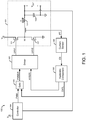
- FIG. 1 illustrates a power converter circuit 100 according to an embodiment.
- Power converter circuit 100 includes power train circuit 101, driver circuit 102, gate circuit 103, controller circuit 104, current sensor circuit 105, and hysteretic comparison circuit 106.
- Power train circuit 101 includes a main switching transistor 111, an auxiliary switching transistor 112, an inductor 114, and an output capacitor 116.
- Main switching transistor 111 may be, for example, a P-channel field effect transistor (FET), and auxiliary switching transistor 112 may be, for example, an N-channel FET.
- Transistors 111 and 112 may be, for example, power metal oxide semiconductor field-effect transistors (i.e., power MOSFETs). Transistors 111 and 112 act as switches.
- Power converter circuit 100 may also be referred to as a switching voltage regulator circuit or a DC/DC converter circuit.
- switching transistors 111-112, driver circuit 102, gate circuit 103, current sensor circuit 105, and hysteretic comparison circuit 106 are all in one integrated circuit (IC), and controller circuit 104 is in a separate integrated circuit.
- controller circuit 104 is in a separate integrated circuit.
- one or more of the circuits in power train circuit 101, such as inductor 114 and capacitor 116, are discrete components.
- Power train circuit 101 receives an input voltage V IN at an input from a source of electrical power and generates a regulated output voltage V OUT at an output node based on the input voltage V IN .
- Power converter 100 converts the input voltage V IN into the output voltage V OUT .
- Power train circuit 101 shown in FIG. 1 employs a step-down (buck) converter topology that converts an input voltage V IN into an output voltage V OUT that is less than the input voltage V IN .
- V IN in FIG. 1 is greater than V OUT .
- the output voltage V OUT of power converter circuit 100 is provided to a load that is coupled to the output node of power converter circuit 100.
- the load may be, for example, a microprocessor integrated circuit, a field programmable gate array integrated circuit, or any other type of circuit or system that draws current.
- Power converter circuit 100 provides output current to the load at V OUT , and the load draws current from power converter circuit 100.
- Power converter circuit 100 alternately turns the switching transistors 111-112 on and off to provide output current to the load and to maintain the output voltage V OUT at a substantially constant voltage.
- the output capacitor 116 is coupled between the output node of power converter circuit 100 and a ground node that is at a ground voltage. Output capacitor 116 filters V OUT to help maintain V OUT at a substantially constant DC voltage.
- Driver circuit 102 generates two drive voltages DRV1 and DRV2 that are provided to the gates of transistors 111 and 112, respectively.
- Driver circuit 102 controls the conductive states of the switching transistors 111 and 112 by controlling the drive voltages DRV1 and DRV2, respectively.
- Driver circuit 102 switches transistors 111 and 112 out of phase, such that when one of transistors 111-112 is on, the other one of transistors 111-112 is off.
- Power converter circuit 100 prevents transistors 111 and 112 from being on at the same time. During each switching period of transistors 111-112, transistor 111 is on and transistor 112 is off for a primary portion of the switching period, and transistor 111 is off and transistor 112 is on for a complementary portion of the switching period.
- the on-times of switching transistors 111 and 112 may be separated by small time intervals in each switching period during which both of transistors 111-112 are off to avoid cross-conduction there between.
- driver circuit 102 maintains transistor 111 off, and driver circuit 102 maintains transistor 112 on, causing the inductor 114 to be coupled to a ground node at the source of transistor 112 that is at the ground voltage.
- transistor 112 provides a circuit path to maintain the continuity of the inductor current IL flowing through the inductor 114.
- the current IL flowing through inductor 114 decreases in response to current flowing through transistor 112 between the ground node and inductor 114.
- the controller circuit 104 generates one or more PWM signals to control the duty cycles of the switching transistors 111-112 using driver circuit 102.
- Controller circuit 104 may be referred to as a pulse-width modulation (PWM) controller circuit.
- the one or more PWM signals generated by controller circuit 104 are provided to one or more inputs of gate circuit 103.
- Gate circuit 103 may be, for example, a logic gate circuit, such as an AND or a NAND logic gate circuit.
- Hysteretic comparison circuit 106 generates a control signal CNTL that is provided to an additional input of gate circuit 103.
- Gate circuit 103 generates signals PWMDR at its outputs.
- Power converter circuit 100 operates in at least three modes of operation that are referred to as a pulse width modulation (PWM) mode, a positive current limit mode, and a negative current limit mode.
- PWM pulse width modulation
- hysteretic comparison circuit 106 causes the control signal CNTL to have a value that causes gate circuit 103 to pass the values of the PWM signals to the outputs of gate circuit 103 in signals PWMDR.
- gate circuit 103 is an AND gate or a NAND gate
- hysteretic comparison circuit 106 drives control signal CNTL to a logic high state during pulse width modulation mode, causing gate circuit 103 to drive signals PWMDR to the same values as signals PWM.
- Signals PWMDR are provided to inputs of driver circuit 102.
- Driver circuit 102 generates the drive voltages DRV1 and DRV2 based on the PWMDR signals during PWM mode.
- driver circuit 102 turns on transistor 111 and turns off transistor 112.
- driver circuit 102 turns off transistor 111 and turns on transistor 112.
- Controller circuit 104 causes the PWM and PWMDR signals to alternate between the first and second values during PWM mode.
- Controller circuit 104 receives the input voltage V IN and the output voltage V OUT at inputs. Controller circuit 104 generates the PWM signals in response to the input voltage V IN and in response to the output voltage V OUT . During the pulse width modulation mode, controller circuit 104 varies the PWM and the PWMDR signals to vary the duty cycles of the switching transistors 111-112 in order to regulate the output voltage V OUT and to maintain the output voltage V OUT at a substantially constant voltage.
- controller circuit 104 may include a comparator circuit that compares the output voltage V OUT (or a divided down version of V OUT ) to a reference voltage. In response to V OUT decreasing below a target voltage for V OUT that is indicated by the reference voltage, controller circuit 104 adjusts the PWM and PWMDR signals to cause driver circuit 102 to maintain transistor 111 on and transistor 112 off for a longer period of time during each switching period of transistors 111-112.
- controller circuit 104 and driver circuit 102 increase the duty cycle of transistor 111 and decrease the duty cycle of transistor 112 in response to V OUT decreasing below the target voltage, causing the current IL in inductor 114 to increase and causing V OUT to increase to the target voltage.
- controller circuit 104 adjusts the PWM and PWMDR signals to cause driver circuit 102 to maintain transistor 112 on and transistor 111 off for a longer period of time during each switching period of transistors 111-112.
- controller circuit 104 and driver circuit 102 decrease the duty cycle of transistor 111 and increase the duty cycle of transistor 112 in response to V OUT increasing above the target voltage, causing the current IL in inductor 114 to decrease and causing V OUT to decrease to the target voltage.
- Controller circuit 104 and driver circuit 102 maintain the duty cycles of transistors 111-112 constant in response to V OUT being at the target voltage. Controller circuit 104 and driver circuit 102 may also vary the duty cycles of switching transistors 111-112 in response to changes in the input voltage V IN during the pulse width modulation mode.
- Current sensor circuit 105 senses a current IPT in power train circuit 101.
- Current sensor circuit 105 generates a current sense signal CS based on the current IPT.
- Current sensor circuit 105 causes the current sense signal CS to be indicative of the current IPT in power train circuit 101.
- Current sensor circuit 105 continuously monitors the current IPT in power train circuit 101 during each on-time of switching transistor 111 and during each on-time of switching transistor 112.
- Current sensor circuit 105 may be in the same integrated circuit (IC) with transistors 111-112, or current sensor circuit 105 may be in a separate IC. Current sensor circuit 105 can measure a positive current or a negative current in power train circuit 101.
- a positive current in power train circuit 101 may refer to the inductor current IL flowing from node N1 to V OUT , as shown by the direction of the arrow in Figure 1 .
- a negative current in power train circuit 101 may refer to the inductor current IL flowing in the opposite direction as a positive current.
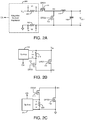
- Figures 2A-2C illustrate some examples of current sensor circuit 105, according to various embodiments.
- Figure 2A illustrates an example of current sensor circuit 105 that includes an integrated current replicator circuit 200, according to an embodiment.
- the integrated current replicator circuit 200 includes two current sense resistors 201-202 having known resistances, two transconductance amplifiers (not shown), and additional circuitry (not shown).
- Resistor 201 is coupled between the input voltage V IN and the source of switching transistor 111. When transistor 111 is on, current flows through resistor 201 and transistor 111, generating a first voltage V1 across resistor 201, as shown in FIG. 2A . Voltage V1 and the resistance of resistor 201 indicate the current through resistor 201 and transistor 111 when transistor 111 is on.
- the first transconductance amplifier generates a first current signal indicative of the voltage V1 across resistor 201.
- Resistor 202 is coupled between the source of switching transistor 112 and the ground node. When transistor 112 is on, current flows through transistor 112 and resistor 202, generating a second voltage V2 across resistor 202, as shown in FIG. 2A . Voltage V2 and the resistance of resistor 202 indicate the current through resistor 202 and transistor 112 when transistor 112 is on. The second transconductance amplifier generates a second current signal indicative of the voltage V2 across resistor 202.
- Integrated current replicator circuit 200 includes an additional amplifier circuit that generates the current sense signal CS based on the first and second current signals generated by the transconductance amplifiers. Further details of an integrated current replicator, such as integrated current replicator circuit 200 are disclosed in commonly-assigned U.S. patent application 20150280558, filed March 27, 2014 , which is incorporated by reference herein in its entirety.
- Integrated current replicator circuit 200 can measure a positive current or a negative current through either of resistors 201 or 202. Integrated current replicator circuit 200 can measure a positive current flowing through resistor 201 from V IN to transistor 111 or a negative current flowing through resistor 201 from transistor 111 to V IN . Integrated current replicator circuit 200 can also measure a positive current flowing through resistor 202 from the ground node to transistor 112 or a negative current flowing through resistor 202 from transistor 112 to the ground node.
- Figures 2B-2C illustrate another example of current sensor circuit 105 that includes two resistors, two transistors, and operational amplifiers, according to another embodiment.
- Figure 2B illustrates a sense resistor 210, a P-channel FET 211, and an operational amplifier (op amp) circuit 215.
- Resistor 210 and transistor 211 are coupled in parallel with switching transistor 111.
- the gate of transistor 211 is coupled to receive the same drive signal DRV1 from driver circuit 102 that is provided to the gate of transistor 111.
- driver circuit 102 turns transistors 111 and 211 on concurrently during each switching period.
- transistors 111 and 211 are on, a current flows through sense resistor 210 and transistor 211 that is a fraction of the current flowing through the main switching transistor 111.
- the voltage V1 across resistor 210 is proportional to the current through resistor 210. Voltage V1 is provided to inputs of operational amplifier circuit 215. The op amp circuit 215 causes the current sense signal CS to indicate the current through transistor 111 while transistor 111 is on.
- Figure 2C illustrates a sense resistor 220, an N-channel FET 212, and an operational amplifier (op amp) circuit 217.
- Resistor 220 and transistor 212 are coupled in parallel with switching transistor 112.
- the gate of transistor 212 is coupled to receive the same drive signal DRV2 from driver circuit 102 that is provided to the gate of transistor 112.
- driver circuit 102 turns transistors 112 and 212 on concurrently during each switching period.
- transistors 112 and 212 are on, a current flows through sense resistor 220 and transistor 212 that is a fraction of the current flowing through switching transistor 112.
- the voltage V2 across resistor 220 is proportional to the current through resistor 220.
- Voltage V2 is provided to inputs of operational amplifier circuit 217.
- Op amp circuit 217 causes the current sense signal CS to indicate the current through transistor 112 while transistor 112 is on.
- the current sensor circuit of Figures 2B-2C can measure a positive current or a negative current through either one of resistors 210 or 220.
- Op amp 215 can measure a positive current flowing through resistor 210 from V IN to node N1 or a negative current flowing through resistor 210 from node N1 to V IN .
- Op amp 217 can measure a positive current flowing through resistor 220 from the ground node to node N1 or a negative current flowing through resistor 220 from node N1 to the ground node.
- current sensor circuit 105 includes circuitry that uses direct-current resistance (DCR) current sensing.
- current sensor circuit 105 includes a series resistor-capacitor (RC) network that is coupled in parallel with inductor 114.
- the RC network uses DCR current sensing to measure the current through inductor 114 by measuring the resistance of inductor 114.
- the resistor and the capacitor in the RC network of current sensor circuit 105 are selected to cause the RC time constant of the RC network to be equal to an L/R L time constant of inductor 114, where L is the inductance of inductor 114, and R L is the DC resistance of inductor 114.
- This embodiment can also be used to measure a positive current or a negative current in power train circuit 101.
- FIG. 3 illustrates an example of hysteretic comparison circuit 106, according to an embodiment.
- hysteretic comparison circuit 106 includes a first hysteretic comparator circuit 301, a second hysteretic comparator circuit 302, and a NOR gate circuit 303.
- the current sense signal CS is a voltage signal.
- the current sense signal CS is provided to the non-inverting input of hysteretic comparator circuit 301.
- a first reference voltage VREFA is provided to the inverting input of hysteretic comparator circuit 301.
- Hysteretic comparator circuit 301 generates a first hysteretic drive signal HYSDR1 at its output that is based on the difference between the voltage of signal CS and reference voltage VREFA.
- the current sense signal CS is also provided to the inverting input of hysteretic comparator circuit 302.
- a second reference voltage VREFB is provided to the non-inverting input of hysteretic comparator circuit 302.
- Hysteretic comparator circuit 302 generates a second hysteretic drive signal HYSDR2 at its output that is based on the difference between reference voltage VREFB and the voltage of signal CS.
- Hysteretic drive signals HYSDR1 and HYSDR2 are collectively referred to as hysteretic drive signals HYSDR in Figure 1 .
- a hysteretic comparator such as hysteretic comparator circuits 301 and 302, has two thresholds.
- a hysteretic comparator determines which of its two thresholds to apply to the input voltage of the hysteretic comparator based on the current state (high or low) of the output voltage of the hysteretic comparator.
- Each of the hysteretic comparator circuits 301-302 may include, for example, a comparator or amplifier circuit coupled to a positive feedback loop circuit. The positive feedback loop circuit causes the hysteretic comparator to be responsive to the state of its output voltage in order to determine which of its two thresholds to compare to its input voltage.
- Hysteretic comparator circuit 301 has a first threshold VTPU and a second threshold VTPL.
- the first threshold VTPU and the second threshold VTPL represent two different voltage thresholds. The difference between VTPU and VTPL equals the hysteresis of comparator circuit 301.
- the first threshold VTPU is indicative of a positive current limit ITPU for the current through power train circuit 101.
- power converter circuit 100 In response to the current through power train circuit 101 reaching the positive current limit ITPU, power converter circuit 100 enters the positive current limit mode.
- the second threshold VTPL is indicative of a positive minimum current ITPL of the positive current limit mode. In response to the current through power train circuit 101 reaching the positive minimum current ITPL, power converter circuit 100 exits the positive current limit mode and returns to pulse width modulation mode.
- the first threshold VTPU and the second threshold VTPL of hysteretic comparator circuit 301 are determined by the reference voltage VREFA and other characteristics of comparator circuit 301.
- the reference voltage VREFA may be programmably adjustable by a user or by other circuitry to vary the thresholds of hysteretic comparator circuit 301.
- hysteretic comparator circuit 301 monitors the current sense signal CS to determine when a positive current through power train circuit 101 increases to equal or exceed the positive current limit ITPU.
- the current sense signal CS rising to the first threshold VTPU of hysteretic comparator circuit 301 indicates that the current through power train circuit 101 has increased to the positive current limit ITPU.
- hysteretic comparator circuit 301 In response to the current sense signal CS increasing to the first threshold VTPU of hysteretic comparator circuit 301, hysteretic comparator circuit 301 asserts the drive signal HYSDR1 to a logic high state, causing NOR gate circuit 303 to de-assert the CNTL signal to a logic low state, and causing power converter 100 to enter the positive current limit mode.
- gate circuit 103 prevents the values of the PWM signals from propagating to the PWMDR signals.
- hysteretic comparison circuit 106 prevents the PWM signals from controlling the conductive states of switching transistors 111-112 during the positive current limit mode.
- driver circuit 102 In response to receiving a logic high state in the drive signal HYSDR1, driver circuit 102 turns transistor 111 off if transistor 111 is on and turns transistor 112 on if transistor 112 is off. Driver circuit 102 maintains the main switching transistor 111 off and maintains the auxiliary switching transistor 112 on during the positive current limit mode in response to the logic high state in drive signal HYSDR1. As a result of transistor 111 being off and transistor 112 being on, the current IL through the inductor 114 decreases. By causing the inductor current IL to decrease in the positive current limit mode, the current limit circuit prevents the current through power train circuit 101 from substantially exceeding the positive current limit ITPU. Although in some embodiments, delay in the current limit circuit may allow the current through power train circuit 101 to briefly exceed the positive current limit ITPU.
- hysteretic comparator circuit 301 monitors the current sense signal CS to determine when the current through power train circuit 101 has decreased to be equal to or less than the positive minimum current ITPL of the positive current limit mode.
- the current sense signal CS falling to the second threshold VTPL of hysteretic comparator circuit 301 indicates that the current through power train circuit 101 has decreased to the positive minimum current ITPL of the positive current limit mode.
- hysteretic comparator circuit 301 In response to the current sense signal CS decreasing to the second threshold VTPL of hysteretic comparator circuit 301, hysteretic comparator circuit 301 de-asserts the drive signal HYSDR1 to a logic low state, causing NOR gate circuit 303 to assert the CNTL signal to a logic high state, and causing power converter 100 to re-enter the pulse width modulation mode.
- the output signal HYSDR2 of hysteretic comparator circuit 302 When power converter circuit 100 is in the positive current limit mode, the output signal HYSDR2 of hysteretic comparator circuit 302 is in a logic low state, and therefore, the output signal CNTL of NOR gate circuit 303 is controlled by comparator circuit 301.
- gate circuit 103 In response to the CNTL signal being in a logic high state, gate circuit 103 passes the values of the PWM signals to signals PWMDR. In response to driver circuit 102 receiving a logic low state in drive signal HYSDR1, driver circuit 102 controls the conductive states of transistors 111 and 112 based on the PWMDR signals, which equal the values of the corresponding PWM signals. Controller circuit 104 then controls the conductive states of transistors 111-112 again using the PWM signals in pulse width modulation mode. Controller circuit 104 and driver circuit 102 control the current IL through inductor 114 in response to the current drawn by the load as indicated by the output voltage V OUT during pulse width modulation mode as described above.
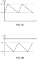
- Figure 4A is a timing diagram that illustrates an example of the current through power train circuit 101 as power converter circuit 100 enters and exits the positive current limit mode, according to an embodiment.
- the current through the power train circuit 101 increases until the current reaches the positive current limit ITPU.
- power converter circuit 100 enters the positive current limit mode, and the current through the power train 101 decreases as described above.
- the current through power train 101 then decreases to the positive minimum current ITPL.
- power converter circuit 100 enters the pulse width modulation mode again.
- the current through power train 101 may increase or decrease in pulse width modulation mode depending on the current drawn by the load. In the example of FIG. 4A , the current drawn by the load is greater than the positive current limit ITPU. Therefore, power converter circuit 100 increases the current through power train 101 during each pulse width modulation mode until the positive current limit ITPU is reached.
- hysteretic comparator circuit 302 has a first threshold VTNU and a second threshold VTNL.
- the first threshold VTNU and the second threshold VTNL represent two different voltage thresholds.
- the difference between VTNU and VTNL equals the hysteresis of comparator circuit 302.
- the first threshold VTNU is indicative of a negative current limit -ITNU (i.e., a maximum negative current) for the current through power train circuit 101.
- the second threshold VTNL is indicative of a minimum negative current -ITNL of the negative current limit mode.
- power converter circuit 100 exits the negative current limit mode and returns to pulse width modulation mode.
- the first threshold VTNU and the second threshold VTNL of hysteretic comparator circuit 302 are determined by the reference voltage VREFB and other characteristics of comparator circuit 302.
- the reference voltage VREFB may be programmably adjustable by a user or by other circuitry to vary the thresholds of hysteretic comparator circuit 302. Because two different programmable reference voltages VREFA and VREFB are used to determine the thresholds of comparator circuits 301 and 302, respectively, the negative current limit -ITNU can be programmed to be a different current value than the absloute value of the positive current limit ITPU. Alternatively, the negative current limit -ITNU can be programmed to be the absloute value of the positive current limit ITPU.
- hysteretic comparator circuit 302 monitors the current sense signal CS to determine when a negative current through power train circuit 101 reaches or exceeds the negative current limit -ITNU.
- the current through power train circuit 101 is a negative current when the inductor current IL flows in the opposite direction of the arrow shown for IL in Figure 1 from inductor 114 through transistor 111 to V IN or through transistor 112 to ground. Negative current may flow through power train 101, for example, if the load suddenly transitions from drawing a heavy load current to drawing a light load current from power converter 100.
- the current sense signal CS decreasing to the first threshold VTNU of hysteretic comparator circuit 302 indicates that a negative current through power train circuit 101 has reached the negative current limit -ITNU.
- hysteretic comparator circuit 302 asserts its output drive signal HYSDR2 to a logic high state, causing NOR gate circuit 303 to de-assert the CNTL signal to a logic low state, and causing power converter 100 to enter the negative current limit mode.
- gate circuit 103 prevents the values of the PWM signals from propagating to the PWMDR signals.
- hysteretic comparison circuit 106 prevents the PWM signals from controlling the conductive states of switching transistors 111-112 during the negative current limit mode.
- hysteretic comparator circuit 302 monitors the current sense signal CS to determine when the negative current through power train circuit 101 has decreased to be equal to or less than the minimum negative current -ITNL of the negative current limit mode.
- the current sense signal CS increasing to the second threshold VTNL of hysteretic comparator circuit 302 indicates that the negative current through power train circuit 101 has decreased to the minimum negative current -ITNL of the negative current limit mode.
- hysteretic comparator circuit 302 In response to the current sense signal CS increasing to the second threshold VTNL of hysteretic comparator circuit 302, hysteretic comparator circuit 302 de-asserts its output drive signal HYSDR2 to a logic low state, causing NOR gate circuit 303 to assert the CNTL signal to a logic high state, and causing power converter 100 to re-enter the pulse width modulation mode.
- the output signal HYSDR1 of hysteretic comparator circuit 301 When power converter 100 is in the negative current limit mode, the output signal HYSDR1 of hysteretic comparator circuit 301 is in a logic low state, and therefore, the output signal CNTL of NOR gate circuit 303 is controlled by comparator circuit 302.
- gate circuit 103 In response to the CNTL signal being in a logic high state, gate circuit 103 passes the values of the PWM signals to signals PWMDR. In response to driver circuit 102 receiving a logic low state in drive signal HYSDR2, driver circuit 102 controls the conductive states of transistors 111 and 112 based on the PWMDR signals. Controller circuit 104 then controls the conductive states of transistors 111-112 again using the PWM signals during pulse width modulation mode. Controller circuit 104 and driver circuit 102 control the current through power train 101 in response to the current drawn by the load as indicated by the output voltage V OUT during pulse width modulation mode as described above.
- Figure 4B is a timing diagram that illustrates an example of the current through power train circuit 101 as power converter circuit 100 enters and exits the negative current limit mode, according to an embodiment.
- the negative current through power train circuit 101 increases until the negative current reaches the negative current limit -ITNU.
- power converter circuit 100 enters the negative current limit mode, and the negative current through the power train 101 decreases as described above.
- the negative current through power train 101 then decreases to the minimum negative current -ITNL of the negative current limit mode.
- power converter circuit 100 enters the pulse width modulation mode again.
- the current through the power train circuit 101 varies in pulse width modulation mode depending on the current drawn by the load.
- the negative current through power train circuit 101 increases during each pulse width modulation mode until the negative current limit -ITNU is reached.
- -ITNL and -ITNU may be -40 amps and -60 amps, respectively.
- Figure 5 is a flow chart showing operations that may be performed to determine when power converter circuit 100 enters and exits the positive current limit mode, according to an embodiment.
- power converter circuit 100 continuously monitors the current through power train circuit 101 using current sensor circuit 105 and hysteretic comparison circuit 106.
- hysteretic comparison circuit 106 determines that the current through power train circuit 101 has reached the positive current limit ITPU, for example, as described with respect to Figure 3 .
- hysteretic comparison circuit 106 controls the conductive states of switching transistors 111-112 in the positive current limit mode to reduce the current through power train circuit 101, as described above.
- hysteretic comparison circuit 106 determines that the current through power train circuit 101 has reached the positive minimum current ITPL, as described above. In operation 504, hysteretic comparison circuit 106 allows controller circuit 104 to control the conductive states of switching transistors 111-112 in pulse width modulation mode using the PWM signals, as described above. In operation 504, power converter circuit 100 exits the positive current limit mode. Power converter circuit 100 may subsequently return to operation 501 if the current in power train 101 reaches ITPU again.
- Figure 6 is a flow chart showing operations that may be performed to determine when power converter circuit 100 enters and exits the negative current limit mode, according to an embodiment.
- hysteretic comparison circuit 106 determines that a negative current in power train circuit 101 has reached the negative current limit -ITNU, for example, as described with respect to Figure 3 .
- hysteretic comparison circuit 106 controls the conductive states of switching transistors 111-112 in the negative current limit mode to decrease the negative current in power train circuit 101, as described above.
- hysteretic comparison circuit 106 determines that the current in power train circuit 101 has reached the minimum negative current -ITNL, as described above.
- a power converter circuit includes two power train circuits 101, two driver circuits 102, and a single one of each of the circuits 103-106 shown in Figure 1 .
- Each driver circuit 102 controls the current in one of the two power train circuits 101.
- driver circuits 102 control power train circuits 101 in PWM mode based on the PWM signals generated by the single controller circuit 104.
- Driver circuits 102 control the currents in power train circuits 101 in the positive and negative current limit modes in response to the output drive signals HYSDR of the single hysteretic comparison circuit 106, as described above.
- the techniques disclosed herein with respect to measuring and limiting a positive current in a power train circuit can be employed in a power train circuit in which switching transistor 112 is replaced with a diode.
- Current in the diode only flows in the positive direction from ground to inductor 114.
- Current sensor circuit 105 and hysteretic comparison circuit 106 limit the outgoing positive current through the power train circuit to the load as disclosed herein.
- Embodiment 1 is a power converter circuit comprising: a current sensor circuit that generates an indication of a current through a power train circuit, wherein the power converter circuit controls the current through the power train circuit; and a hysteretic comparison circuit that compares the indication of the current through the power train circuit to a negative current limit, wherein the power converter circuit causes a negative current in the power train circuit that is flowing away from an output node of the power train circuit to decrease in response to an indication generated by the hysteretic comparison circuit that the negative current in the power train circuit has reached the negative current limit.
- Embodiment 2 is the power converter circuit of embodiment 1 further comprising: a controller circuit that generates a pulse width modulation signal in response to a signal from the power train circuit, wherein the power converter circuit controls the current through the power train circuit in response to the pulse width modulation signal during a pulse width modulation mode; and a gate circuit that prevents the power converter circuit from controlling the current through the power train circuit using the pulse width modulation signal in response to the indication generated by the hysteretic comparison circuit that the negative current in the power train circuit has reached the negative current limit.
- Embodiment 3 is the power converter circuit of embodiment 1, wherein the current sensor circuit continuously monitors the current through the power train circuit to generate the indication of the current through the power train circuit during an on time of a first switching transistor in the power train circuit and during an on time of a second switching transistor in the power train circuit.
- Embodiment 4 is the power converter circuit of embodiment 1, wherein the hysteretic comparison circuit comprises: a first hysteretic comparator circuit that generates a first drive signal by comparing first and second thresholds to a current sense signal, wherein the current sensor circuit generates the current sense signal as the indication of the current through the power train circuit, and wherein the power converter circuit controls the current through the power train circuit in response to the first drive signal during a negative current limit mode.
- Embodiment 6 is the power converter circuit of embodiment 4, wherein the hysteretic comparison circuit further comprises: a second hysteretic comparator circuit that generates a second drive signal by comparing third and fourth thresholds to the current sense signal, wherein the power converter circuit controls the current through the power train circuit in response to the second drive signal during a positive current limit mode.
- Embodiment 8 is the power converter circuit of embodiment 7, further comprising: a controller circuit that generates a pulse width modulation signal in response to a signal from the power train circuit to control the current through the power train circuit and to regulate an output voltage at the output node during a pulse width modulation mode, wherein the hysteretic comparison circuit further comprises a first logic gate circuit that performs a logic function on the first and second drive signals to generate a control signal, wherein the first logic gate circuit de-asserts the control signal to indicate that the current through the power train circuit has reached the negative current limit or the positive current limit; and a second logic gate circuit that prevents the power converter circuit from controlling the current through the power train circuit using the pulse width modulation signal in response to the control signal being de-asserted.
- a controller circuit that generates a pulse width modulation signal in response to a signal from the power train circuit to control the current through the power train circuit and to regulate an output voltage at the output node during a pulse width modulation mode
- Embodiment 9 is the power converter circuit of embodiment 1, wherein the power train circuit comprises first and second switching transistors, wherein the power converter circuit controls current through an inductor by controlling conductive states of the first and second switching transistors, wherein the first switching transistor is coupled between an input node at an input voltage and the inductor, and wherein the second switching transistor is coupled between the inductor and a ground node.
- Embodiment 10 is a power converter circuit comprising: a power train circuit comprising a first switching transistor, wherein the power converter circuit turns the first switching transistor on and off in response to a pulse width modulation signal in a pulse width modulation mode to control a current in the power train circuit; a hysteretic comparison circuit that causes the power converter circuit to control the current in the power train circuit in a first current limit mode in response to the current in the power train circuit reaching a first current limit; and a gate circuit that prevents the power converter circuit from controlling the current in the power train circuit using the pulse width modulation signal during the first current limit mode in response to the hysteretic comparison circuit indicating that the current in the power train circuit has reached the first current limit.
- Embodiment 12 is the power converter circuit of embodiment 10 further comprising: a current sensor circuit that monitors the current in the power train circuit to generate a signal indicative of the current in the power train circuit during an on time of the first switching transistor and during an on time of a second switching transistor in the power train circuit, wherein the signal indicative of the current in the power train circuit is provided to the hysteretic comparison circuit.
- Embodiment 15 is the power converter circuit of embodiment 13, wherein the hysteretic comparison circuit compares the signal indicative of the current in the power train circuit to a second threshold that is indicative of a second current limit, wherein the power converter circuit causes the current in the power train circuit to decrease in a second current limit mode in response to the hysteretic comparison circuit indicating that a positive current in the power train circuit that is flowing toward the output node of the power train circuit has reached the second current limit.
- Embodiment 18 is the method of embodiment 17 further comprising: generating a signal indicative of the positive current and the negative current in the power train circuit using a current sensor circuit during an on time of a first switching transistor in the power train circuit and during an on time of a second switching transistor in the power train circuit, wherein the hysteretic comparison circuit generates the indication that the positive current in the power train circuit has reached the positive current limit and the indication that the negative current in the power train circuit has reached the negative current limit in response to the signal indicative of the positive current and the negative current in the power train circuit.
- Embodiment 19 is the method of embodiment 17 further comprising: exiting the positive current limit mode in response to the positive current in the power train circuit reaching a positive minimum current of the positive current limit mode; and exiting the negative current limit mode in response to the negative current in the power train circuit reaching a minimum negative current of the negative current limit mode.
- Embodiment 20 is the method of embodiment 17 further comprising: generating a pulse width modulation signal using a controller circuit in response to a signal from the power train circuit to control a current in the power train circuit in a pulse width modulation mode; and preventing the controller circuit from controlling the current in the power train circuit in the pulse width modulation mode in response to the indication that the positive current in the power train circuit has reached the positive current limit or in response to the indication that the negative current in the power train circuit has reached the negative current limit.
Applications Claiming Priority (1)
| Application Number | Priority Date | Filing Date | Title |
|---|---|---|---|
| US15/154,497 US20170331363A1 (en) | 2016-05-13 | 2016-05-13 | Current Limited Power Converter Circuits And Methods |
Publications (1)
| Publication Number | Publication Date |
|---|---|
| EP3244518A1 true EP3244518A1 (de) | 2017-11-15 |
Family
ID=58638803
Family Applications (1)
| Application Number | Title | Priority Date | Filing Date |
|---|---|---|---|
| EP17168548.0A Ceased EP3244518A1 (de) | 2016-05-13 | 2017-04-27 | Strombegrenzte leistungswandlerschaltungen und verfahren |
Country Status (3)
| Country | Link |
|---|---|
| US (1) | US20170331363A1 (de) |
| EP (1) | EP3244518A1 (de) |
| CN (1) | CN107370371A (de) |
Cited By (1)
| Publication number | Priority date | Publication date | Assignee | Title |
|---|---|---|---|---|
| CN112148061A (zh) * | 2019-06-28 | 2020-12-29 | 聚积科技股份有限公司 | 补偿式电流校正装置 |
Families Citing this family (4)
| Publication number | Priority date | Publication date | Assignee | Title |
|---|---|---|---|---|
| KR102323560B1 (ko) * | 2017-08-08 | 2021-11-08 | 삼성전자주식회사 | 전류의 피크 세기를 조절하도록 구성되는 회로를 포함하는 전자 장치 |
| CN112769332B (zh) * | 2020-12-25 | 2022-05-24 | 南京矽力微电子技术有限公司 | 功率变换器 |
| US11575321B2 (en) | 2021-02-09 | 2023-02-07 | Navitas Semiconductor Limited | Systems and methods for automatic determination of state of switches in power converters |
| US11949333B2 (en) * | 2021-12-29 | 2024-04-02 | Texas Instruments Incorporated | Peak current limit management for high frequency buck converter |
Citations (3)
| Publication number | Priority date | Publication date | Assignee | Title |
|---|---|---|---|---|
| US20100156368A1 (en) * | 2008-12-19 | 2010-06-24 | Active-Semi, Inc. | Power converters with switched capacitor buck/boost |
| US20150280558A1 (en) | 2014-03-27 | 2015-10-01 | Altera Corporation | Integrated current replicator and method of operating the same |
| EP3010131A1 (de) * | 2014-10-15 | 2016-04-20 | Dialog Semiconductor (UK) Ltd | Gleichstromabwärtswandler mit Taktimpulsfrequenzmodulation |
Family Cites Families (5)
| Publication number | Priority date | Publication date | Assignee | Title |
|---|---|---|---|---|
| CN102570793B (zh) * | 2011-12-07 | 2014-09-17 | 西安启芯微电子有限公司 | Dc-dc变换器中的功率管工作尺寸切换电路 |
| JP5969221B2 (ja) * | 2012-02-29 | 2016-08-17 | エスアイアイ・セミコンダクタ株式会社 | ボルテージレギュレータ |
| US8879217B2 (en) * | 2012-06-29 | 2014-11-04 | Infineon Technologies Austria Ag | Switching regulator with negative current limit protection |
| US8884597B2 (en) * | 2012-07-20 | 2014-11-11 | Fairchild Semiconductor Corporation | Synchronous buck converter with dynamically adjustable low side gate driver |
| DE102012112184A1 (de) * | 2012-12-12 | 2014-06-12 | Sma Solar Technology Ag | Verfahren und Vorrichtung zum Schutz mehrerer Strings eines Photovoltaikgenerators vor Rückströmen |
-
2016
- 2016-05-13 US US15/154,497 patent/US20170331363A1/en not_active Abandoned
-
2017
- 2017-04-27 EP EP17168548.0A patent/EP3244518A1/de not_active Ceased
- 2017-05-12 CN CN201710333548.1A patent/CN107370371A/zh active Pending
Patent Citations (3)
| Publication number | Priority date | Publication date | Assignee | Title |
|---|---|---|---|---|
| US20100156368A1 (en) * | 2008-12-19 | 2010-06-24 | Active-Semi, Inc. | Power converters with switched capacitor buck/boost |
| US20150280558A1 (en) | 2014-03-27 | 2015-10-01 | Altera Corporation | Integrated current replicator and method of operating the same |
| EP3010131A1 (de) * | 2014-10-15 | 2016-04-20 | Dialog Semiconductor (UK) Ltd | Gleichstromabwärtswandler mit Taktimpulsfrequenzmodulation |
Cited By (3)
| Publication number | Priority date | Publication date | Assignee | Title |
|---|---|---|---|---|
| CN112148061A (zh) * | 2019-06-28 | 2020-12-29 | 聚积科技股份有限公司 | 补偿式电流校正装置 |
| EP3758450A1 (de) * | 2019-06-28 | 2020-12-30 | Macroblock, Inc. | Stromversorgungssystem mit stromkompensation |
| CN112148061B (zh) * | 2019-06-28 | 2021-10-08 | 聚积科技股份有限公司 | 补偿式电流校正装置 |
Also Published As
| Publication number | Publication date |
|---|---|
| US20170331363A1 (en) | 2017-11-16 |
| CN107370371A (zh) | 2017-11-21 |
Similar Documents
| Publication | Publication Date | Title |
|---|---|---|
| EP3244518A1 (de) | Strombegrenzte leistungswandlerschaltungen und verfahren | |
| US9529373B2 (en) | Switching regulator and control circuit and control method therefor | |
| TWI458240B (zh) | 根據操作模式控制切換模式電源供應器的切換拓撲的電源供應器系統、切換調整器及方法 | |
| US8384367B2 (en) | Step-down switching regulator | |
| CN105305818B (zh) | 用于开关电源电流采样的系统和方法 | |
| TWI531883B (zh) | 用於低待機電流切換調節器的方法及設備 | |
| US9069370B2 (en) | Digital low drop-out regulator | |
| TWI539256B (zh) | 用於切換模式調節器之動態下降之系統與方法 | |
| EP1801959A2 (de) | Pulsfrequenzregulator mit modulierter Spannung und mit linearer Regulatorsteuerung | |
| JP6209022B2 (ja) | スイッチングレギュレータ | |
| US9195246B2 (en) | Virtual output voltage sensing for feed-forward control of a voltage regulator | |
| US20100026270A1 (en) | Average input current limit method and apparatus thereof | |
| US9740218B2 (en) | Limiting a current | |
| TW201644170A (zh) | 具有分離的高頻及低頻路徑信號的快速暫態電力供應器 | |
| US9397559B2 (en) | Switching regulator current mode feedback circuits and methods | |
| US7196499B1 (en) | DC/DC converter with inductor current sensing capability | |
| JP5803946B2 (ja) | スイッチングレギュレータ | |
| US8686704B2 (en) | Current sense circuit and switching regulator using the same | |
| GB2469370A (en) | Switching regulator suitable for a light source | |
| US9413240B2 (en) | Power converter and controller device | |
| JP2017005774A (ja) | デジタル制御電源回路、その制御回路、制御方法およびそれを用いた電子機器 | |
| US11183935B2 (en) | Current control for buck-boost converters using conditional offsets | |
| US20220149729A1 (en) | Automatic frequency oscillator for pulse-regulated switch-mode power supply | |
| US9647546B2 (en) | Dual-mode voltage doubling buck converter with smooth mode transition | |
| JP6629593B2 (ja) | 電源回路およびその制御回路、制御方法、ならびにそれを用いた電子機器 |
Legal Events
| Date | Code | Title | Description |
|---|---|---|---|
| PUAI | Public reference made under article 153(3) epc to a published international application that has entered the european phase |
Free format text: ORIGINAL CODE: 0009012 |
|
| STAA | Information on the status of an ep patent application or granted ep patent |
Free format text: STATUS: THE APPLICATION HAS BEEN PUBLISHED |
|
| AK | Designated contracting states |
Kind code of ref document: A1 Designated state(s): AL AT BE BG CH CY CZ DE DK EE ES FI FR GB GR HR HU IE IS IT LI LT LU LV MC MK MT NL NO PL PT RO RS SE SI SK SM TR |
|
| AX | Request for extension of the european patent |
Extension state: BA ME |
|
| STAA | Information on the status of an ep patent application or granted ep patent |
Free format text: STATUS: REQUEST FOR EXAMINATION WAS MADE |
|
| 17P | Request for examination filed |
Effective date: 20180509 |
|
| RBV | Designated contracting states (corrected) |
Designated state(s): AL AT BE BG CH CY CZ DE DK EE ES FI FR GB GR HR HU IE IS IT LI LT LU LV MC MK MT NL NO PL PT RO RS SE SI SK SM TR |
|
| STAA | Information on the status of an ep patent application or granted ep patent |
Free format text: STATUS: EXAMINATION IS IN PROGRESS |
|
| 17Q | First examination report despatched |
Effective date: 20190730 |
|
| STAA | Information on the status of an ep patent application or granted ep patent |
Free format text: STATUS: EXAMINATION IS IN PROGRESS |
|
| STAA | Information on the status of an ep patent application or granted ep patent |
Free format text: STATUS: EXAMINATION IS IN PROGRESS |
|
| STAA | Information on the status of an ep patent application or granted ep patent |
Free format text: STATUS: THE APPLICATION HAS BEEN REFUSED |
|
| 18R | Application refused |
Effective date: 20220814 |