EP3758450A1 - Stromversorgungssystem mit stromkompensation - Google Patents
Stromversorgungssystem mit stromkompensation Download PDFInfo
- Publication number
- EP3758450A1 EP3758450A1 EP20181535.4A EP20181535A EP3758450A1 EP 3758450 A1 EP3758450 A1 EP 3758450A1 EP 20181535 A EP20181535 A EP 20181535A EP 3758450 A1 EP3758450 A1 EP 3758450A1
- Authority
- EP
- European Patent Office
- Prior art keywords
- terminal
- coupled
- current
- voltage
- receive
- Prior art date
- Legal status (The legal status is an assumption and is not a legal conclusion. Google has not performed a legal analysis and makes no representation as to the accuracy of the status listed.)
- Granted
Links
Images



Classifications
-
- H—ELECTRICITY
- H02—GENERATION; CONVERSION OR DISTRIBUTION OF ELECTRIC POWER
- H02M—APPARATUS FOR CONVERSION BETWEEN AC AND AC, BETWEEN AC AND DC, OR BETWEEN DC AND DC, AND FOR USE WITH MAINS OR SIMILAR POWER SUPPLY SYSTEMS; CONVERSION OF DC OR AC INPUT POWER INTO SURGE OUTPUT POWER; CONTROL OR REGULATION THEREOF
- H02M3/00—Conversion of DC power input into DC power output
- H02M3/02—Conversion of DC power input into DC power output without intermediate conversion into AC
- H02M3/04—Conversion of DC power input into DC power output without intermediate conversion into AC by static converters
- H02M3/10—Conversion of DC power input into DC power output without intermediate conversion into AC by static converters using discharge tubes with control electrode or semiconductor devices with control electrode
- H02M3/145—Conversion of DC power input into DC power output without intermediate conversion into AC by static converters using discharge tubes with control electrode or semiconductor devices with control electrode using devices of a triode or transistor type requiring continuous application of a control signal
- H02M3/155—Conversion of DC power input into DC power output without intermediate conversion into AC by static converters using discharge tubes with control electrode or semiconductor devices with control electrode using devices of a triode or transistor type requiring continuous application of a control signal using semiconductor devices only
-
- H—ELECTRICITY
- H05—ELECTRIC TECHNIQUES NOT OTHERWISE PROVIDED FOR
- H05B—ELECTRIC HEATING; ELECTRIC LIGHT SOURCES NOT OTHERWISE PROVIDED FOR; CIRCUIT ARRANGEMENTS FOR ELECTRIC LIGHT SOURCES, IN GENERAL
- H05B45/00—Circuit arrangements for operating light-emitting diodes [LED]
- H05B45/30—Driver circuits
- H05B45/345—Current stabilisation; Maintaining constant current
-
- G—PHYSICS
- G05—CONTROLLING; REGULATING
- G05F—SYSTEMS FOR REGULATING ELECTRIC OR MAGNETIC VARIABLES
- G05F1/00—Automatic systems in which deviations of an electric quantity from one or more predetermined values are detected at the output of the system and fed back to a device within the system to restore the detected quantity to its predetermined value or values, i.e. retroactive systems
- G05F1/10—Regulating voltage or current
- G05F1/46—Regulating voltage or current wherein the variable actually regulated by the final control device is DC
- G05F1/56—Regulating voltage or current wherein the variable actually regulated by the final control device is DC using semiconductor devices in series with the load as final control devices
-
- G—PHYSICS
- G05—CONTROLLING; REGULATING
- G05F—SYSTEMS FOR REGULATING ELECTRIC OR MAGNETIC VARIABLES
- G05F3/00—Non-retroactive systems for regulating electric variables by using an uncontrolled element, or an uncontrolled combination of elements, such element or such combination having self-regulating properties
- G05F3/02—Regulating voltage or current
- G05F3/08—Regulating voltage or current wherein the variable is DC
- G05F3/10—Regulating voltage or current wherein the variable is DC using uncontrolled devices with non-linear characteristics
- G05F3/16—Regulating voltage or current wherein the variable is DC using uncontrolled devices with non-linear characteristics being semiconductor devices
- G05F3/20—Regulating voltage or current wherein the variable is DC using uncontrolled devices with non-linear characteristics being semiconductor devices using diode- transistor combinations
- G05F3/26—Current mirrors
-
- H—ELECTRICITY
- H02—GENERATION; CONVERSION OR DISTRIBUTION OF ELECTRIC POWER
- H02M—APPARATUS FOR CONVERSION BETWEEN AC AND AC, BETWEEN AC AND DC, OR BETWEEN DC AND DC, AND FOR USE WITH MAINS OR SIMILAR POWER SUPPLY SYSTEMS; CONVERSION OF DC OR AC INPUT POWER INTO SURGE OUTPUT POWER; CONTROL OR REGULATION THEREOF
- H02M1/00—Details of apparatus for conversion
- H02M1/08—Circuits specially adapted for the generation of control voltages for semiconductor devices incorporated in static converters
-
- H—ELECTRICITY
- H03—ELECTRONIC CIRCUITRY
- H03K—PULSE TECHNIQUE
- H03K19/00—Logic circuits, i.e. having at least two inputs acting on one output; Inverting circuits
- H03K19/0175—Coupling arrangements; Interface arrangements
- H03K19/017509—Interface arrangements
-
- H—ELECTRICITY
- H03—ELECTRONIC CIRCUITRY
- H03K—PULSE TECHNIQUE
- H03K3/00—Circuits for generating electric pulses; Monostable, bistable or multistable circuits
- H03K3/02—Generators characterised by the type of circuit or by the means used for producing pulses
- H03K3/027—Generators characterised by the type of circuit or by the means used for producing pulses by the use of logic circuits, with internal or external positive feedback
- H03K3/037—Bistable circuits
-
- H—ELECTRICITY
- H03—ELECTRONIC CIRCUITRY
- H03K—PULSE TECHNIQUE
- H03K3/00—Circuits for generating electric pulses; Monostable, bistable or multistable circuits
- H03K3/02—Generators characterised by the type of circuit or by the means used for producing pulses
- H03K3/53—Generators characterised by the type of circuit or by the means used for producing pulses by the use of an energy-accumulating element discharged through the load by a switching device controlled by an external signal and not incorporating positive feedback
- H03K3/57—Generators characterised by the type of circuit or by the means used for producing pulses by the use of an energy-accumulating element discharged through the load by a switching device controlled by an external signal and not incorporating positive feedback the switching device being a semiconductor device
-
- H—ELECTRICITY
- H05—ELECTRIC TECHNIQUES NOT OTHERWISE PROVIDED FOR
- H05B—ELECTRIC HEATING; ELECTRIC LIGHT SOURCES NOT OTHERWISE PROVIDED FOR; CIRCUIT ARRANGEMENTS FOR ELECTRIC LIGHT SOURCES, IN GENERAL
- H05B45/00—Circuit arrangements for operating light-emitting diodes [LED]
- H05B45/10—Controlling the intensity of the light
-
- H—ELECTRICITY
- H05—ELECTRIC TECHNIQUES NOT OTHERWISE PROVIDED FOR
- H05B—ELECTRIC HEATING; ELECTRIC LIGHT SOURCES NOT OTHERWISE PROVIDED FOR; CIRCUIT ARRANGEMENTS FOR ELECTRIC LIGHT SOURCES, IN GENERAL
- H05B45/00—Circuit arrangements for operating light-emitting diodes [LED]
- H05B45/20—Controlling the colour of the light
-
- H—ELECTRICITY
- H05—ELECTRIC TECHNIQUES NOT OTHERWISE PROVIDED FOR
- H05B—ELECTRIC HEATING; ELECTRIC LIGHT SOURCES NOT OTHERWISE PROVIDED FOR; CIRCUIT ARRANGEMENTS FOR ELECTRIC LIGHT SOURCES, IN GENERAL
- H05B45/00—Circuit arrangements for operating light-emitting diodes [LED]
- H05B45/30—Driver circuits
- H05B45/32—Pulse-control circuits
-
- H—ELECTRICITY
- H05—ELECTRIC TECHNIQUES NOT OTHERWISE PROVIDED FOR
- H05B—ELECTRIC HEATING; ELECTRIC LIGHT SOURCES NOT OTHERWISE PROVIDED FOR; CIRCUIT ARRANGEMENTS FOR ELECTRIC LIGHT SOURCES, IN GENERAL
- H05B45/00—Circuit arrangements for operating light-emitting diodes [LED]
- H05B45/30—Driver circuits
- H05B45/37—Converter circuits
- H05B45/3725—Switched mode power supply [SMPS]
- H05B45/375—Switched mode power supply [SMPS] using buck topology
-
- H—ELECTRICITY
- H05—ELECTRIC TECHNIQUES NOT OTHERWISE PROVIDED FOR
- H05B—ELECTRIC HEATING; ELECTRIC LIGHT SOURCES NOT OTHERWISE PROVIDED FOR; CIRCUIT ARRANGEMENTS FOR ELECTRIC LIGHT SOURCES, IN GENERAL
- H05B45/00—Circuit arrangements for operating light-emitting diodes [LED]
- H05B45/40—Details of LED load circuits
- H05B45/44—Details of LED load circuits with an active control inside an LED matrix
- H05B45/48—Details of LED load circuits with an active control inside an LED matrix having LEDs organised in strings and incorporating parallel shunting devices
-
- H—ELECTRICITY
- H02—GENERATION; CONVERSION OR DISTRIBUTION OF ELECTRIC POWER
- H02M—APPARATUS FOR CONVERSION BETWEEN AC AND AC, BETWEEN AC AND DC, OR BETWEEN DC AND DC, AND FOR USE WITH MAINS OR SIMILAR POWER SUPPLY SYSTEMS; CONVERSION OF DC OR AC INPUT POWER INTO SURGE OUTPUT POWER; CONTROL OR REGULATION THEREOF
- H02M1/00—Details of apparatus for conversion
- H02M1/0003—Details of control, feedback or regulation circuits
- H02M1/0009—Devices or circuits for detecting current in a converter
Definitions
- the disclosure relates to a power supply system, and more particularly to a power supply system with current compensation.
- FIG. 1 illustrates a conventional hysteretic power supply system for dimming control of multiple light emitting diodes (LEDs) (LED_R, LED_G, LED_B, LED_W).
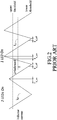
- a switch (M1) is switched to an OFF state when an inductor current (i.e., a current flowing through an inductor (L1)) increases to become greater than an upper threshold, and is switched to an ON state when the inductor current decreases to become smaller than a lower threshold.
- An average of the inductor current is expected to be constantly equal to an average of the upper and lower thresholds.
- dimming of the LEDs can be adjusted by changing operating states of switches (M_S1-M_S4).
- a voltage across the LEDs (LED_R, LED_G, LED_B, LED_W) changes with a number (K), which is a number of one(s) of the LEDs (LED_R, LED_G, LED_B, LED_W) that emit(s) light. Accordingly, an increase slope, a decrease slope, a crest, a trough, the average of the inductor current, and brightness of each of the one(s) of the LEDs (LED_R, LED_G, LED_B, LED_W) that emit(s) light also change with the number (K). As shown in FIG.
- K 1 during a time period (I)
- K 2 during a time period (II)
- K 3 during a time period (III)
- K 4 during a time period (IV)
- the average of the inductor current (I AVG ) decreases with increasing K.
- an object of the disclosure is to provide a power supply system with current compensation.
- the power supply system can alleviate the drawback of the prior art.
- the power supply system is operatively associated with a load unit.
- the load unit includes a first terminal, a second terminal, and a plurality of loads that are coupled in series between the first and second terminals thereof.
- the power supply system includes a current driver circuit, a sensor circuit, a control circuit, a voltage generator circuit and a signal generator circuit.
- the current driver circuit is to receive a pulse signal, and generates an output current based on the pulse signal. The output current increases within each pulse of the pulse signal, and decreases outside each pulse of the pulse signal.
- the sensor circuit is coupled to the current driver circuit, and is adapted to be further coupled to the first terminal of the load unit.
- the sensor circuit allows the output current to flow therethrough from the current driver circuit to the first terminal of the load unit, and senses the output current to generate a sensed voltage.
- the control circuit is adapted to be coupled to the loads, and is to receive a control input. For each of the loads, the control circuit is operable, based on the control input, to allow or not to allow the output current to flow through the load.
- the voltage generator circuit is to receive the control input, and generates a reference voltage based on the control input. The reference voltage is correlated to a number of one(s) of the loads through which the output current flows.
- the signal generator circuit is coupled to the sensor circuit, the voltage generator circuit and the current driver circuit, and is to receive the sensed voltage and the reference voltage respectively from the sensor circuit and the voltage generator circuit. The signal generator circuit generates a first threshold voltage and a second threshold voltage based on the reference voltage, and compares the sensed voltage with the first and second threshold voltages to generate the pulse signal for receipt by the current driver circuit.
- an embodiment of a power supply system is operatively associated with a load unit 100.
- the load unit 100 includes a first terminal, a second terminal that is coupled to ground, and a number (N) of loads 1 that are coupled in series between the first and second terminals thereof, where N is an integer greater than one.
- N 4
- the loads 1 are respectively light emitting diodes (LEDs) 101-104 of different colors in this embodiment.
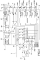
- the power supply system of this embodiment includes a current driver circuit 2, a sensor circuit 3, a control circuit 4, a voltage generator circuit 5 and a signal generator circuit 6.
- the current driver circuit 2 is to receive a pulse signal (GATE), and generates an output current (I L ) based on the pulse signal (GATE).
- the output current (I L ) increases within each pulse of the pulse signal (GATE), and decreases outside each pulse of the pulse signal (GATE).
- the current driver circuit 2 includes a switch (Q1), a diode 22 and an inductor 23.
- the switch (Q1) e.g., an N-type metal oxide semiconductor field effect transistor (nMOSFET)
- nMOSFET N-type metal oxide semiconductor field effect transistor
- the pulse signal (GATE) transitions between an active state (e.g., a logic "1" state) and an inactive state (e.g., a logic "0" state).
- the switch (Q) is in the ON state when the pulse signal (GATE) is in the active state (i.e., within each pulse of the pulse signal (GATE)), and is in the OFF state when the pulse signal (GATE) is in the inactive state (i.e., outside each pulse of the pulse signal (GATE)).
- the diode 22 e.g., a Schottky diode
- the inductor 23 has a first terminal that is coupled to the second terminal of the switch (Q1), and a second terminal that provides the output current (I L ).
- the sensor circuit 3 is coupled to the current driver circuit 2, and is adapted to be further coupled to the first terminal of the load unit 100.
- the sensor circuit 3 allows the output current (I L ) to flow therethrough from the current driver circuit 2 to the first terminal of the load unit 100, and senses the output current (I L ) to generate a sensed voltage (V Sense ).
- the sensor circuit 3 includes a resistor 31 and an amplifier 32.
- the resistor 31 has a first terminal that is coupled to the second terminal of the inductor 23 to receive the output current (I L ) therefrom, and a second terminal that is adapted to be coupled to the first terminal of the load unit 100 to provide the output current (I L ) thereto.
- the amplifier 32 has a non-inverting input terminal that is coupled to the first terminal of the resistor 31, an inverting input terminal that is coupled to the second terminal of the resistor 31, and an output terminal that provides the sensed voltage (V Sense ).
- the control circuit 4 is adapted to be coupled to the LEDs 101-104, and is to receive a control input. For each of the LEDs 101-104, the control circuit 4 is operable, based on the control input, to allow or not to allow the output current (I L ) to flow through the LED. Each of the LEDs 101-104 emits light when the output current (I L ) flows therethrough.
- control input includes a number (N) (i.e., four) of control signals (DIMR, DIMG, DIMB, DIMW).
- Each of the control signals (DIMR, DIMG, DIMB, DIMW) transitions between an active state (e.g., a logic "1" state) and an inactive state (e.g., a logic "0" state).
- the control circuit 4 includes a number (N) (i.e., four) of switches (M41-M44) and a controller 42.
- Each of the switches (M41-M44) e.g., an nMOSFET) is adapted to be coupled to a respective one of the LEDs 101-104 in parallel.
- the controller 42 is coupled to the switches (M41-M44), is to receive the control signals (DIMR, DIMG, DIMB, DIMW), and controls operation of each of the switches (M41-M44) between an ON state and an OFF state based on a respective one of the control signals (DIMR, DIMG, DIMB, DIMW).
- the controller 42 performs bootstrapping and inverting to generate a number (N) (i.e., four) of signals (GATER, GATEG, GATEB, GATEW), which are respectively complementary to the control signals (DIMR, DIMG, DIMB, DIMW), to respectively control the operations of the switches (M41-M44).
- Each of the switches (M41-M44) is in the OFF state and the output current (I L ) flows through the respective one of the LEDs 101-104 when the respective one of the control signals (DIMR, DIMG, DIMB, DIMW) is in the active state.
- Each of the switches (M41-M44) is in the ON state and the output current (I L ) flows therethrough when the respective one of the control signals (DIMR, DIMG, DIMB, DIMW) is in the inactive state.
- the voltage generator circuit 5 is to receive the control input, and generates a reference voltage (V REF_COM ) based on the control input.
- the reference voltage (V REF_COM ) is correlated to a number (K), which is a number of one(s) of the LEDs 101-104 through which the output current (I L ) flows (i.e., a number of one(s) of the LEDs 101-104 that emit(s) light).
- the voltage generator circuit 5 includes a first current generator 51, a second current generator 52 and a reference voltage generator 53.
- the first current generator 51 generates a compensation current (I ACC ).
- the second current generator 52 is coupled to the first current generator 51 to receive the compensation current (I ACC ) therefrom, to receive the control input, and generates a reference current based on the compensation current (I ACC ) and the control input.
- the reference current is equal to a product of the compensation current (I ACC ) and the number (K) (i.e., K ⁇ I ACC ).
- the reference voltage generator 53 is coupled to the second current generator 52, is to receive the reference current from the second current generator 52, and generates the reference voltage (V REF_COM ) based on the reference current.
- the first current generator 51 includes a resistor 511, an amplifier 512 and a transistor 513.
- the resistor 511 has a first terminal, a second terminal that is coupled to ground, and a resistance of R ACC .
- the amplifier 512 has a non-inverting input terminal that is to receive a compensation voltage (V ACC ) (e.g., 1.2V), an inverting input terminal that is coupled to the first terminal of the resistor 511, and an output terminal.
- V ACC compensation voltage
- the transistor 513 (e.g., an nMOSFET) has a first terminal (e.g., a drain terminal), a second terminal (e.g., a source terminal) that is coupled to the first terminal of the resistor 511, and a control terminal (e.g., the gate terminal) that is coupled to the output terminal of the amplifier 512.
- the compensation current (I ACC ) is provided at the first terminal of the transistor 513, and is equal to V ACC /R ACC .
- the second current generator 52 includes a current mirror 521 and a number (N) (i.e., four) of switches (MA1-MA4).
- the current mirror 521 is coupled to the first terminal of the transistor 513 to receive the compensation current (I ACC ) therefrom, and generates a number (N) (i.e., four) of mirrored currents based on the compensation current (I ACC ). Each of the mirrored currents is equal to the compensation current (I ACC ).
- Each of the switches (MA1-MA4) (e.g., an nMOSFET) has a first terminal (e.g., a drain terminal), a second terminal (e.g., a source terminal) and a control terminal (e.g., a gate terminal).
- the first terminals of the switches (MA1-MA4) are coupled to the current mirror 521 to respectively receive the mirrored currents therefrom.
- the second terminals of the switches (MA1-MA4) are coupled to each other.
- the control terminals of the switches (MA1-MA4) are to respectively receive the control signals (DIMR, DIMG, DIMB, DIMW).
- the reference current is provided at a common node of the switches (MA1-MA4).
- Each of the switches (MA1-MA4) is in an ON state when a respective one of the control signals (DIMR, DIMG, DIMB, DIMW) is in the active state, and is in an OFF state when the respective one of the control signals (DIMR, DIMG, DIMB, DIMW) is in the inactive state.
- the reference voltage generator 53 includes a resistor 531, an amplifier 532 and a transistor 533.
- the resistor 531 has a first terminal that is coupled to the common node of the switches (MA1-MA4) to receive the reference current therefrom, a second terminal, and a resistance of R ref (e.g., 1KQ).
- the amplifier 532 has a non-inverting input terminal that is coupled to the second terminal of the resistor 531, an inverting input terminal that is to receive a base voltage (V REF ) (e.g., 1V), and an output terminal.
- V REF base voltage
- the transistor 533 (e.g., an nMOSFET) has a first terminal (e.g., a drain terminal) that is coupled to the second terminal of the resistor 531, a second terminal (e.g., a source terminal) that is coupled to ground, and a control terminal (e.g., a gate terminal) that is coupled to the output terminal of the amplifier 532.
- the signal generator circuit 6 is coupled to the sensor circuit 3, the voltage generator circuit 5 and the current driver circuit 2, and is to receive the sensed voltage (V Sense ) and the reference voltage (V REF_COM ) respectively from the sensor circuit 3 and the voltage generator circuit 5.
- the signal generator circuit 6 generates a first threshold voltage (V HB ) and a second threshold voltage (V LB ) based on the reference voltage (V REF_COM ), and compares the sensed voltage (V Sense ) with the first and second threshold voltages (V HB , V LB ) to generate the pulse signal (GATE) for receipt by the current driver circuit (2).
- the signal generator circuit 6 includes a threshold voltage generator 61, a first comparator 62, a second comparator 63, an RS flip-flop 64 and a level shifter 65.
- the threshold voltage generator 61 is coupled to the first terminal of the resistor 531 to receive the reference voltage (V REF_COM ) therefrom, and generates the first and second threshold voltages (V HB , V LB ) based on the reference voltage (V REF_COM ).
- the second threshold voltage (V LB ) is lower than the first threshold voltage (V HB ), and an average of the first and second threshold voltages (V HB , V LB ) is equal to the reference voltage (V REF_COM ).
- the first comparator 62 has an inverting input terminal that is coupled to the threshold voltage generator 61 to receive the first threshold voltage (V HB ) therefrom, a non-inverting input terminal that is coupled to the output terminal of the amplifier 32 to receive the sensed voltage (V Sense ) therefrom, and an output terminal.
- the second comparator 63 has an inverting input terminal that is coupled to the output terminal of the amplifier 32 to receive the sensed voltage (V Sense ) therefrom, a non-inverting input terminal that is coupled to the threshold voltage generator 61 to receive the second threshold voltage (V LB ) therefrom, and an output terminal.
- the RS flip-flop 64 has a reset terminal that is coupled to the output terminal of the first comparator 62, a set terminal that is coupled to the output terminal of the second comparator 63, and an output terminal that provides an intermediate signal (PWM).
- the level shifter 65 is coupled to the output terminal of the RS flip-flop 64 to receive the intermediate signal (PWM) therefrom, is further coupled to the control terminal of the switch (Q1), and performs bootstrapping to translate the intermediate signal (PWM) from a voltage domain to another voltage domain to generate the pulse signal (GATE) for receipt by the control terminal of the switch (Q1).
- the pulse signal (GATE) is set to the logic "1" state when the second comparator 63 determines that the sensed voltage (V Sense ) is lower than the second threshold voltage (V LB ), and is reset to the logic "0" state when the first comparator 62 determines that the sensed voltage (V Sense ) is higher than the first threshold voltage (V HB ).
- FIGS. 4 and 5 operations of the power supply system of this embodiment are described in detail below.
- the output current (I L ), the pulse signal (GATE), the sensed voltage (V Sense ), the intermediate signal (PWM), a voltage across the LEDs 101-104 (V ISN ), the reference voltage (V REF_COM ) and the control signals (DIMR, DIMG, DIMB, DIMW) are depicted.
- three of the control signals (e.g., DIMG, DIMB, DIMW) are in the logic "1" state, and one of the control signals (e.g., DIMR) is in the logic "0" state.
- the switches (MA2-MA4) are in the ON state, and the switch (MA1) is in the OFF state, so the reference voltage (V REF_COM ) is equal to V REF +3 ⁇ V.
- An increase slop and an decrease slop of the sensed voltage (V Sense ) are respectively faster and slower during the second time period than during the first time period, so a difference between a crest of the sensed voltage (V Sense ) and the first threshold voltage (V HB ) and a difference between a trough of the sensed voltage (V Sense ) and the second threshold voltage (V LB ) are respectively larger and smaller during the second time period than during the first time period.
- two of the control signals e.g., DIMB, DIMW
- two of the control signals e.g., DIMR, DIMG
- the switches (MA3, MA4) are in the ON state, and the switches (MA1, MA2) are in the OFF state, so the reference voltage (V REF_COM ) is equal to V REF +2 ⁇ V.
- the increase slop and the decrease slop of the sensed voltage (V Sense ) are respectively faster and slower during the third time period than during the second time period, so the difference between the crest of the sensed voltage (V Sense ) and the first threshold voltage (V HB ) and the difference between the trough of the sensed voltage (V Sense ) and the second threshold voltage (V LB ) are respectively larger and smaller during the third time period than during the second time period.
- one of the control signals (e.g., DIMW) are in the logic "1" state, and three of the control signals (e.g., DIMR, DIMG, DIMB) are in the logic "0" state.
- the switch (MA4) is in the ON state, and the switches (MA1-MA3) are in the OFF state, so the reference voltage (V REF_COM ) is equal to V REF +AV.
- the increase slop and the decrease slop of the sensed voltage (V Sense ) are respectively faster and slower during the fourth time period than during the third time period, so the difference between the crest of the sensed voltage (V Sense ) and the first threshold voltage (V HB ) and the difference between the trough of the sensed voltage (V Sense ) and the second threshold voltage (V LB ) are respectively larger and smaller during the fourth time period than during the third time period.
- the average of the output current (I AVG ) is substantially constant, and almost does not change with the number (K); in a scenario where the working voltages of the LEDs 101-104 are different, the average of the output current (I AVG ) changes with the number (K) slightly as compared to the conventional hysteretic power supply system.
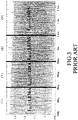
- FIG. 6 illustrates measurement result of the output current (I L ). As shown in FIG. 6 , the number (K) are different in time periods (I-IV), and the average of the output current (I AVG ) is substantially the same in the time periods (I-IV).
- the voltage generator circuit 5 adjusting the reference voltage (V REF_COM ) according to the number (K), and by virtue of the signal generator circuit 6 generating the first and second threshold voltages (V HB , V LB ) based on the reference voltage (V REF_COM ), the change of the average of the output current (I AVG ) (see FIG. 5 ) with the number (K) can be reduced or even eliminated.
Landscapes
- Engineering & Computer Science (AREA)
- Physics & Mathematics (AREA)
- Electromagnetism (AREA)
- General Physics & Mathematics (AREA)
- Radar, Positioning & Navigation (AREA)
- Automation & Control Theory (AREA)
- Computer Hardware Design (AREA)
- Power Engineering (AREA)
- Nonlinear Science (AREA)
- Microelectronics & Electronic Packaging (AREA)
- Computing Systems (AREA)
- General Engineering & Computer Science (AREA)
- Mathematical Physics (AREA)
- Circuit Arrangement For Electric Light Sources In General (AREA)
- Control Of Indicators Other Than Cathode Ray Tubes (AREA)
- Control Of El Displays (AREA)
- Dc-Dc Converters (AREA)
Applications Claiming Priority (1)
| Application Number | Priority Date | Filing Date | Title |
|---|---|---|---|
| TW108122920A TWI697257B (zh) | 2019-06-28 | 2019-06-28 | 補償式電流校正裝置 |
Publications (2)
| Publication Number | Publication Date |
|---|---|
| EP3758450A1 true EP3758450A1 (de) | 2020-12-30 |
| EP3758450B1 EP3758450B1 (de) | 2023-01-25 |
Family
ID=71130863
Family Applications (1)
| Application Number | Title | Priority Date | Filing Date |
|---|---|---|---|
| EP20181535.4A Active EP3758450B1 (de) | 2019-06-28 | 2020-06-23 | Stromversorgungssystem mit stromkompensation |
Country Status (6)
| Country | Link |
|---|---|
| US (1) | US11114939B2 (de) |
| EP (1) | EP3758450B1 (de) |
| JP (1) | JP6931250B2 (de) |
| KR (1) | KR102411963B1 (de) |
| CN (1) | CN112148061B (de) |
| TW (1) | TWI697257B (de) |
Families Citing this family (3)
| Publication number | Priority date | Publication date | Assignee | Title |
|---|---|---|---|---|
| CN113271702B (zh) * | 2021-05-07 | 2023-02-28 | 华润微集成电路(无锡)有限公司 | 一种自适应调节三通道彩灯led恒流驱动电路和方法 |
| US12191767B2 (en) | 2021-06-02 | 2025-01-07 | Mediatek Singapore Pte. Ltd. | Apparatus and method for applying dynamic compensation to feedback signal generated from loadline of voltage regulator |
| USD1030254S1 (en) * | 2023-12-19 | 2024-06-11 | Sandra Tartaglione | Item of clothing with attached towel and attached loop |
Citations (4)
| Publication number | Priority date | Publication date | Assignee | Title |
|---|---|---|---|---|
| US20050046399A1 (en) * | 2003-09-03 | 2005-03-03 | Delta Electronics, Inc. | Power supply having efficient low power standby mode |
| CN202183892U (zh) * | 2010-10-12 | 2012-04-04 | 技领半导体(上海)有限公司 | 单电感器多led灯串的驱动器 |
| US20170079112A1 (en) * | 2015-09-11 | 2017-03-16 | Luxmill Electronic Co., Ltd. | Multi-Stage Led Driving Circuit Capable of Eliminating Current Undershoot |
| EP3244518A1 (de) * | 2016-05-13 | 2017-11-15 | Altera Corporation | Strombegrenzte leistungswandlerschaltungen und verfahren |
Family Cites Families (18)
| Publication number | Priority date | Publication date | Assignee | Title |
|---|---|---|---|---|
| US7688045B2 (en) * | 2006-08-07 | 2010-03-30 | Addtek Corp. | DC power conversion circuit with constant current output |
| ES2369233T3 (es) * | 2007-12-07 | 2011-11-28 | Koninklijke Philips Electronics N.V. | Método y sistema de control del color de lámparas led. |
| CN101646280A (zh) * | 2008-08-05 | 2010-02-10 | 马善学 | Led高压节能电源 |
| TWI580305B (zh) * | 2008-09-05 | 2017-04-21 | 艾杜雷控股有限公司 | 以發光二極體為光源之照明系統 |
| US10264637B2 (en) * | 2009-09-24 | 2019-04-16 | Cree, Inc. | Solid state lighting apparatus with compensation bypass circuits and methods of operation thereof |
| KR101677728B1 (ko) * | 2009-10-26 | 2016-11-21 | 페어차일드코리아반도체 주식회사 | 역률 보상 회로 및 역률 보상 회로의 구동 방법 |
| KR101129287B1 (ko) * | 2010-05-11 | 2012-03-27 | 주식회사 디엠비테크놀로지 | Led 구동 시스템 |
| KR101674217B1 (ko) * | 2010-12-21 | 2016-11-09 | 매그나칩 반도체 유한회사 | 기준전압 생성회로 및 이를 이용한 led 구동회로 |
| US8866392B2 (en) * | 2011-08-31 | 2014-10-21 | Chia-Teh Chen | Two-level LED security light with motion sensor |
| EP2852258B1 (de) * | 2012-05-18 | 2018-11-21 | Koito Manufacturing Co., Ltd. | Lichtquellensteuerungsvorrichtung |
| US9661697B2 (en) * | 2013-03-14 | 2017-05-23 | Laurence P. Sadwick | Digital dimmable driver |
| JP6307302B2 (ja) * | 2014-02-19 | 2018-04-04 | 株式会社小糸製作所 | 車両用灯具およびその駆動装置 |
| CN104270874B (zh) * | 2014-10-27 | 2017-07-18 | 无锡华润矽科微电子有限公司 | 分段式led驱动电路 |
| JP6529452B2 (ja) * | 2016-03-11 | 2019-06-12 | 日立オートモティブシステムズ株式会社 | モータ駆動装置及びモータ駆動装置における相電流検出方法 |
| CN107276434B (zh) * | 2016-04-18 | 2019-08-13 | 南京矽力杰半导体技术有限公司 | 同步整流电路及其控制方法 |
| JP6804364B2 (ja) * | 2017-03-29 | 2020-12-23 | 富士通セミコンダクターメモリソリューション株式会社 | 整流回路および電子装置 |
| WO2019092114A1 (en) * | 2017-11-13 | 2019-05-16 | Signify Holding B.V. | Solid state lighting circuit and control method |
| CN208572491U (zh) * | 2018-06-21 | 2019-03-01 | 上海晶丰明源半导体股份有限公司 | 控制电路、led驱动芯片及led驱动系统 |
-
2019
- 2019-06-28 TW TW108122920A patent/TWI697257B/zh active
-
2020
- 2020-05-26 CN CN202010453138.2A patent/CN112148061B/zh active Active
- 2020-06-18 US US16/905,725 patent/US11114939B2/en active Active
- 2020-06-23 EP EP20181535.4A patent/EP3758450B1/de active Active
- 2020-06-24 JP JP2020108947A patent/JP6931250B2/ja active Active
- 2020-06-25 KR KR1020200077577A patent/KR102411963B1/ko active Active
Patent Citations (4)
| Publication number | Priority date | Publication date | Assignee | Title |
|---|---|---|---|---|
| US20050046399A1 (en) * | 2003-09-03 | 2005-03-03 | Delta Electronics, Inc. | Power supply having efficient low power standby mode |
| CN202183892U (zh) * | 2010-10-12 | 2012-04-04 | 技领半导体(上海)有限公司 | 单电感器多led灯串的驱动器 |
| US20170079112A1 (en) * | 2015-09-11 | 2017-03-16 | Luxmill Electronic Co., Ltd. | Multi-Stage Led Driving Circuit Capable of Eliminating Current Undershoot |
| EP3244518A1 (de) * | 2016-05-13 | 2017-11-15 | Altera Corporation | Strombegrenzte leistungswandlerschaltungen und verfahren |
Also Published As
| Publication number | Publication date |
|---|---|
| US11114939B2 (en) | 2021-09-07 |
| CN112148061A (zh) | 2020-12-29 |
| JP2021010294A (ja) | 2021-01-28 |
| EP3758450B1 (de) | 2023-01-25 |
| KR102411963B1 (ko) | 2022-06-21 |
| US20200412242A1 (en) | 2020-12-31 |
| KR20210002343A (ko) | 2021-01-07 |
| JP6931250B2 (ja) | 2021-09-01 |
| TWI697257B (zh) | 2020-06-21 |
| CN112148061B (zh) | 2021-10-08 |
| TW202102059A (zh) | 2021-01-01 |
Similar Documents
| Publication | Publication Date | Title |
|---|---|---|
| US7705543B2 (en) | Supply device of circuit branches with LED diodes | |
| US10361620B2 (en) | Voltage converter and operating method of voltage converter | |
| US8933647B2 (en) | LED controller with current-ripple control | |
| EP3758450B1 (de) | Stromversorgungssystem mit stromkompensation | |
| US9198242B2 (en) | Apparatus for driving LEDs using high voltage | |
| US20110057704A1 (en) | Method for detecting a current and compensating for an offset voltage and circuit | |
| US20070069712A1 (en) | Driving circuit and electronic device using the same | |
| US20050007080A1 (en) | Semiconductor device including DC-DC converter control circuit | |
| US20180160492A1 (en) | Led current controller | |
| US20140085952A1 (en) | Synchronous rectifier controller, power converter using same, and method therefor | |
| KR20070111331A (ko) | 차지 펌프의 모드 변환 조절 회로 및 방법 | |
| US20170257916A1 (en) | Lighting device | |
| JP5428254B2 (ja) | Led駆動装置 | |
| US8847500B2 (en) | LED driver and driving method | |
| US10673338B2 (en) | Voltage converter and operating method of voltage converter | |
| US9992826B1 (en) | Dual mode constant current LED driver | |
| CN113841326B (zh) | 具有多个驱动级的开关转换器及相关模式 | |
| US10931198B2 (en) | Buck-boost power converter controller | |
| US8988004B2 (en) | Method of forming a current controller for an LED and structure therefor | |
| US20100033100A1 (en) | Backlight module control system and control method thereof | |
| JP4899112B2 (ja) | Led駆動装置 | |
| JP7249887B2 (ja) | Led制御装置、led駆動装置、及び表示装置 | |
| KR20140086909A (ko) | 차지 펌프 장치 | |
| US20260082469A1 (en) | Light source driving systems and devices | |
| JP5687091B2 (ja) | 電源電圧検出回路 |
Legal Events
| Date | Code | Title | Description |
|---|---|---|---|
| PUAI | Public reference made under article 153(3) epc to a published international application that has entered the european phase |
Free format text: ORIGINAL CODE: 0009012 |
|
| STAA | Information on the status of an ep patent application or granted ep patent |
Free format text: STATUS: THE APPLICATION HAS BEEN PUBLISHED |
|
| AK | Designated contracting states |
Kind code of ref document: A1 Designated state(s): AL AT BE BG CH CY CZ DE DK EE ES FI FR GB GR HR HU IE IS IT LI LT LU LV MC MK MT NL NO PL PT RO RS SE SI SK SM TR |
|
| AX | Request for extension of the european patent |
Extension state: BA ME |
|
| STAA | Information on the status of an ep patent application or granted ep patent |
Free format text: STATUS: REQUEST FOR EXAMINATION WAS MADE |
|
| 17P | Request for examination filed |
Effective date: 20210625 |
|
| RBV | Designated contracting states (corrected) |
Designated state(s): AL AT BE BG CH CY CZ DE DK EE ES FI FR GB GR HR HU IE IS IT LI LT LU LV MC MK MT NL NO PL PT RO RS SE SI SK SM TR |
|
| GRAP | Despatch of communication of intention to grant a patent |
Free format text: ORIGINAL CODE: EPIDOSNIGR1 |
|
| STAA | Information on the status of an ep patent application or granted ep patent |
Free format text: STATUS: GRANT OF PATENT IS INTENDED |
|
| INTG | Intention to grant announced |
Effective date: 20220909 |
|
| GRAS | Grant fee paid |
Free format text: ORIGINAL CODE: EPIDOSNIGR3 |
|
| GRAA | (expected) grant |
Free format text: ORIGINAL CODE: 0009210 |
|
| STAA | Information on the status of an ep patent application or granted ep patent |
Free format text: STATUS: THE PATENT HAS BEEN GRANTED |
|
| AK | Designated contracting states |
Kind code of ref document: B1 Designated state(s): AL AT BE BG CH CY CZ DE DK EE ES FI FR GB GR HR HU IE IS IT LI LT LU LV MC MK MT NL NO PL PT RO RS SE SI SK SM TR |
|
| REG | Reference to a national code |
Ref country code: GB Ref legal event code: FG4D |
|
| REG | Reference to a national code |
Ref country code: CH Ref legal event code: EP |
|
| REG | Reference to a national code |
Ref country code: AT Ref legal event code: REF Ref document number: 1546662 Country of ref document: AT Kind code of ref document: T Effective date: 20230215 Ref country code: IE Ref legal event code: FG4D |
|
| REG | Reference to a national code |
Ref country code: DE Ref legal event code: R096 Ref document number: 602020007785 Country of ref document: DE |
|
| REG | Reference to a national code |
Ref country code: LT Ref legal event code: MG9D |
|
| REG | Reference to a national code |
Ref country code: NL Ref legal event code: MP Effective date: 20230125 |
|
| REG | Reference to a national code |
Ref country code: AT Ref legal event code: MK05 Ref document number: 1546662 Country of ref document: AT Kind code of ref document: T Effective date: 20230125 |
|
| PG25 | Lapsed in a contracting state [announced via postgrant information from national office to epo] |
Ref country code: NL Free format text: LAPSE BECAUSE OF FAILURE TO SUBMIT A TRANSLATION OF THE DESCRIPTION OR TO PAY THE FEE WITHIN THE PRESCRIBED TIME-LIMIT Effective date: 20230125 |
|
| P01 | Opt-out of the competence of the unified patent court (upc) registered |
Effective date: 20230530 |
|
| PG25 | Lapsed in a contracting state [announced via postgrant information from national office to epo] |
Ref country code: RS Free format text: LAPSE BECAUSE OF FAILURE TO SUBMIT A TRANSLATION OF THE DESCRIPTION OR TO PAY THE FEE WITHIN THE PRESCRIBED TIME-LIMIT Effective date: 20230125 Ref country code: PT Free format text: LAPSE BECAUSE OF FAILURE TO SUBMIT A TRANSLATION OF THE DESCRIPTION OR TO PAY THE FEE WITHIN THE PRESCRIBED TIME-LIMIT Effective date: 20230525 Ref country code: NO Free format text: LAPSE BECAUSE OF FAILURE TO SUBMIT A TRANSLATION OF THE DESCRIPTION OR TO PAY THE FEE WITHIN THE PRESCRIBED TIME-LIMIT Effective date: 20230425 Ref country code: LV Free format text: LAPSE BECAUSE OF FAILURE TO SUBMIT A TRANSLATION OF THE DESCRIPTION OR TO PAY THE FEE WITHIN THE PRESCRIBED TIME-LIMIT Effective date: 20230125 Ref country code: LT Free format text: LAPSE BECAUSE OF FAILURE TO SUBMIT A TRANSLATION OF THE DESCRIPTION OR TO PAY THE FEE WITHIN THE PRESCRIBED TIME-LIMIT Effective date: 20230125 Ref country code: HR Free format text: LAPSE BECAUSE OF FAILURE TO SUBMIT A TRANSLATION OF THE DESCRIPTION OR TO PAY THE FEE WITHIN THE PRESCRIBED TIME-LIMIT Effective date: 20230125 Ref country code: ES Free format text: LAPSE BECAUSE OF FAILURE TO SUBMIT A TRANSLATION OF THE DESCRIPTION OR TO PAY THE FEE WITHIN THE PRESCRIBED TIME-LIMIT Effective date: 20230125 Ref country code: AT Free format text: LAPSE BECAUSE OF FAILURE TO SUBMIT A TRANSLATION OF THE DESCRIPTION OR TO PAY THE FEE WITHIN THE PRESCRIBED TIME-LIMIT Effective date: 20230125 |
|
| PG25 | Lapsed in a contracting state [announced via postgrant information from national office to epo] |
Ref country code: SE Free format text: LAPSE BECAUSE OF FAILURE TO SUBMIT A TRANSLATION OF THE DESCRIPTION OR TO PAY THE FEE WITHIN THE PRESCRIBED TIME-LIMIT Effective date: 20230125 Ref country code: PL Free format text: LAPSE BECAUSE OF FAILURE TO SUBMIT A TRANSLATION OF THE DESCRIPTION OR TO PAY THE FEE WITHIN THE PRESCRIBED TIME-LIMIT Effective date: 20230125 Ref country code: IS Free format text: LAPSE BECAUSE OF FAILURE TO SUBMIT A TRANSLATION OF THE DESCRIPTION OR TO PAY THE FEE WITHIN THE PRESCRIBED TIME-LIMIT Effective date: 20230525 Ref country code: GR Free format text: LAPSE BECAUSE OF FAILURE TO SUBMIT A TRANSLATION OF THE DESCRIPTION OR TO PAY THE FEE WITHIN THE PRESCRIBED TIME-LIMIT Effective date: 20230426 Ref country code: FI Free format text: LAPSE BECAUSE OF FAILURE TO SUBMIT A TRANSLATION OF THE DESCRIPTION OR TO PAY THE FEE WITHIN THE PRESCRIBED TIME-LIMIT Effective date: 20230125 |
|
| REG | Reference to a national code |
Ref country code: DE Ref legal event code: R097 Ref document number: 602020007785 Country of ref document: DE |
|
| PG25 | Lapsed in a contracting state [announced via postgrant information from national office to epo] |
Ref country code: SM Free format text: LAPSE BECAUSE OF FAILURE TO SUBMIT A TRANSLATION OF THE DESCRIPTION OR TO PAY THE FEE WITHIN THE PRESCRIBED TIME-LIMIT Effective date: 20230125 Ref country code: RO Free format text: LAPSE BECAUSE OF FAILURE TO SUBMIT A TRANSLATION OF THE DESCRIPTION OR TO PAY THE FEE WITHIN THE PRESCRIBED TIME-LIMIT Effective date: 20230125 Ref country code: EE Free format text: LAPSE BECAUSE OF FAILURE TO SUBMIT A TRANSLATION OF THE DESCRIPTION OR TO PAY THE FEE WITHIN THE PRESCRIBED TIME-LIMIT Effective date: 20230125 Ref country code: DK Free format text: LAPSE BECAUSE OF FAILURE TO SUBMIT A TRANSLATION OF THE DESCRIPTION OR TO PAY THE FEE WITHIN THE PRESCRIBED TIME-LIMIT Effective date: 20230125 Ref country code: CZ Free format text: LAPSE BECAUSE OF FAILURE TO SUBMIT A TRANSLATION OF THE DESCRIPTION OR TO PAY THE FEE WITHIN THE PRESCRIBED TIME-LIMIT Effective date: 20230125 |
|
| PG25 | Lapsed in a contracting state [announced via postgrant information from national office to epo] |
Ref country code: SK Free format text: LAPSE BECAUSE OF FAILURE TO SUBMIT A TRANSLATION OF THE DESCRIPTION OR TO PAY THE FEE WITHIN THE PRESCRIBED TIME-LIMIT Effective date: 20230125 |
|
| PLBE | No opposition filed within time limit |
Free format text: ORIGINAL CODE: 0009261 |
|
| STAA | Information on the status of an ep patent application or granted ep patent |
Free format text: STATUS: NO OPPOSITION FILED WITHIN TIME LIMIT |
|
| 26N | No opposition filed |
Effective date: 20231026 |
|
| PG25 | Lapsed in a contracting state [announced via postgrant information from national office to epo] |
Ref country code: MC Free format text: LAPSE BECAUSE OF FAILURE TO SUBMIT A TRANSLATION OF THE DESCRIPTION OR TO PAY THE FEE WITHIN THE PRESCRIBED TIME-LIMIT Effective date: 20230125 |
|
| PG25 | Lapsed in a contracting state [announced via postgrant information from national office to epo] |
Ref country code: SI Free format text: LAPSE BECAUSE OF FAILURE TO SUBMIT A TRANSLATION OF THE DESCRIPTION OR TO PAY THE FEE WITHIN THE PRESCRIBED TIME-LIMIT Effective date: 20230125 Ref country code: MC Free format text: LAPSE BECAUSE OF FAILURE TO SUBMIT A TRANSLATION OF THE DESCRIPTION OR TO PAY THE FEE WITHIN THE PRESCRIBED TIME-LIMIT Effective date: 20230125 |
|
| REG | Reference to a national code |
Ref country code: CH Ref legal event code: PL |
|
| REG | Reference to a national code |
Ref country code: BE Ref legal event code: MM Effective date: 20230630 |
|
| PG25 | Lapsed in a contracting state [announced via postgrant information from national office to epo] |
Ref country code: LU Free format text: LAPSE BECAUSE OF NON-PAYMENT OF DUE FEES Effective date: 20230623 |
|
| REG | Reference to a national code |
Ref country code: IE Ref legal event code: MM4A |
|
| PG25 | Lapsed in a contracting state [announced via postgrant information from national office to epo] |
Ref country code: LU Free format text: LAPSE BECAUSE OF NON-PAYMENT OF DUE FEES Effective date: 20230623 |
|
| PG25 | Lapsed in a contracting state [announced via postgrant information from national office to epo] |
Ref country code: IE Free format text: LAPSE BECAUSE OF NON-PAYMENT OF DUE FEES Effective date: 20230623 |
|
| PG25 | Lapsed in a contracting state [announced via postgrant information from national office to epo] |
Ref country code: IE Free format text: LAPSE BECAUSE OF NON-PAYMENT OF DUE FEES Effective date: 20230623 Ref country code: CH Free format text: LAPSE BECAUSE OF NON-PAYMENT OF DUE FEES Effective date: 20230630 |
|
| PG25 | Lapsed in a contracting state [announced via postgrant information from national office to epo] |
Ref country code: IT Free format text: LAPSE BECAUSE OF FAILURE TO SUBMIT A TRANSLATION OF THE DESCRIPTION OR TO PAY THE FEE WITHIN THE PRESCRIBED TIME-LIMIT Effective date: 20230125 Ref country code: BE Free format text: LAPSE BECAUSE OF NON-PAYMENT OF DUE FEES Effective date: 20230630 |
|
| PG25 | Lapsed in a contracting state [announced via postgrant information from national office to epo] |
Ref country code: BG Free format text: LAPSE BECAUSE OF FAILURE TO SUBMIT A TRANSLATION OF THE DESCRIPTION OR TO PAY THE FEE WITHIN THE PRESCRIBED TIME-LIMIT Effective date: 20230125 |
|
| PG25 | Lapsed in a contracting state [announced via postgrant information from national office to epo] |
Ref country code: BG Free format text: LAPSE BECAUSE OF FAILURE TO SUBMIT A TRANSLATION OF THE DESCRIPTION OR TO PAY THE FEE WITHIN THE PRESCRIBED TIME-LIMIT Effective date: 20230125 |
|
| PGFP | Annual fee paid to national office [announced via postgrant information from national office to epo] |
Ref country code: DE Payment date: 20250612 Year of fee payment: 6 |
|
| PGFP | Annual fee paid to national office [announced via postgrant information from national office to epo] |
Ref country code: GB Payment date: 20250612 Year of fee payment: 6 |
|
| PGFP | Annual fee paid to national office [announced via postgrant information from national office to epo] |
Ref country code: FR Payment date: 20250612 Year of fee payment: 6 |
|
| PG25 | Lapsed in a contracting state [announced via postgrant information from national office to epo] |
Ref country code: CY Free format text: LAPSE BECAUSE OF FAILURE TO SUBMIT A TRANSLATION OF THE DESCRIPTION OR TO PAY THE FEE WITHIN THE PRESCRIBED TIME-LIMIT; INVALID AB INITIO Effective date: 20200623 |
|
| PG25 | Lapsed in a contracting state [announced via postgrant information from national office to epo] |
Ref country code: HU Free format text: LAPSE BECAUSE OF FAILURE TO SUBMIT A TRANSLATION OF THE DESCRIPTION OR TO PAY THE FEE WITHIN THE PRESCRIBED TIME-LIMIT; INVALID AB INITIO Effective date: 20200623 |
|
| PG25 | Lapsed in a contracting state [announced via postgrant information from national office to epo] |
Ref country code: TR Free format text: LAPSE BECAUSE OF FAILURE TO SUBMIT A TRANSLATION OF THE DESCRIPTION OR TO PAY THE FEE WITHIN THE PRESCRIBED TIME-LIMIT Effective date: 20230125 |