EP3241857B1 - Composition de résine durcissable, objet moulé en résine durcissable, objet durci, produit stratifié, composite et carte à circuit imprimé multicouche - Google Patents
Composition de résine durcissable, objet moulé en résine durcissable, objet durci, produit stratifié, composite et carte à circuit imprimé multicouche Download PDFInfo
- Publication number
- EP3241857B1 EP3241857B1 EP15865344.4A EP15865344A EP3241857B1 EP 3241857 B1 EP3241857 B1 EP 3241857B1 EP 15865344 A EP15865344 A EP 15865344A EP 3241857 B1 EP3241857 B1 EP 3241857B1
- Authority
- EP
- European Patent Office
- Prior art keywords
- curable resin
- compound
- resin composition
- group
- cured object
- Prior art date
- Legal status (The legal status is an assumption and is not a legal conclusion. Google has not performed a legal analysis and makes no representation as to the accuracy of the status listed.)
- Active
Links
- 239000011342 resin composition Substances 0.000 title claims description 107
- 229920005989 resin Polymers 0.000 title claims description 41
- 239000011347 resin Substances 0.000 title claims description 41
- 239000002131 composite material Substances 0.000 title claims description 23
- 150000001875 compounds Chemical class 0.000 claims description 106
- -1 triazole compound Chemical class 0.000 claims description 96
- 239000004593 Epoxy Substances 0.000 claims description 65
- 239000004020 conductor Substances 0.000 claims description 64
- 239000000463 material Substances 0.000 claims description 20
- 238000000034 method Methods 0.000 claims description 17
- 125000004185 ester group Chemical group 0.000 claims description 14
- 125000004435 hydrogen atom Chemical group [H]* 0.000 claims description 14
- 125000004169 (C1-C6) alkyl group Chemical group 0.000 claims description 13
- KLSJWNVTNUYHDU-UHFFFAOYSA-N Amitrole Chemical compound NC1=NC=NN1 KLSJWNVTNUYHDU-UHFFFAOYSA-N 0.000 claims description 13
- 229920001955 polyphenylene ether Polymers 0.000 claims description 10
- 125000002887 hydroxy group Chemical group [H]O* 0.000 claims description 8
- 125000006700 (C1-C6) alkylthio group Chemical group 0.000 claims description 6
- 125000004076 pyridyl group Chemical group 0.000 claims description 6
- 125000002947 alkylene group Chemical group 0.000 claims description 4
- 239000010410 layer Substances 0.000 description 92
- 238000002156 mixing Methods 0.000 description 23
- 239000000758 substrate Substances 0.000 description 19
- 239000000047 product Substances 0.000 description 18
- RYGMFSIKBFXOCR-UHFFFAOYSA-N Copper Chemical compound [Cu] RYGMFSIKBFXOCR-UHFFFAOYSA-N 0.000 description 16
- 239000011256 inorganic filler Substances 0.000 description 16
- 229910003475 inorganic filler Inorganic materials 0.000 description 16
- 239000011889 copper foil Substances 0.000 description 15
- 230000000052 comparative effect Effects 0.000 description 14
- 239000000835 fiber Substances 0.000 description 14
- 239000000203 mixture Substances 0.000 description 13
- 239000002904 solvent Substances 0.000 description 13
- 238000003860 storage Methods 0.000 description 11
- 239000003795 chemical substances by application Substances 0.000 description 10
- 238000010438 heat treatment Methods 0.000 description 10
- YXFVVABEGXRONW-UHFFFAOYSA-N Toluene Chemical compound CC1=CC=CC=C1 YXFVVABEGXRONW-UHFFFAOYSA-N 0.000 description 9
- ZUOUZKKEUPVFJK-UHFFFAOYSA-N diphenyl Chemical compound C1=CC=CC=C1C1=CC=CC=C1 ZUOUZKKEUPVFJK-UHFFFAOYSA-N 0.000 description 8
- 238000004519 manufacturing process Methods 0.000 description 7
- FVCSARBUZVPSQF-UHFFFAOYSA-N 5-(2,4-dioxooxolan-3-yl)-7-methyl-3a,4,5,7a-tetrahydro-2-benzofuran-1,3-dione Chemical compound C1C(C(OC2=O)=O)C2C(C)=CC1C1C(=O)COC1=O FVCSARBUZVPSQF-UHFFFAOYSA-N 0.000 description 6
- 238000001035 drying Methods 0.000 description 6
- 125000003700 epoxy group Chemical group 0.000 description 6
- 239000000126 substance Substances 0.000 description 6
- 239000003112 inhibitor Substances 0.000 description 5
- 239000002184 metal Substances 0.000 description 5
- 229910052751 metal Inorganic materials 0.000 description 5
- 239000000243 solution Substances 0.000 description 5
- 238000012360 testing method Methods 0.000 description 5
- HHPDFYDITNAMAM-UHFFFAOYSA-N 2-[cyclohexyl(2-hydroxyethyl)amino]ethanol Chemical compound OCCN(CCO)C1CCCCC1 HHPDFYDITNAMAM-UHFFFAOYSA-N 0.000 description 4
- LFQSCWFLJHTTHZ-UHFFFAOYSA-N Ethanol Chemical compound CCO LFQSCWFLJHTTHZ-UHFFFAOYSA-N 0.000 description 4
- VYPSYNLAJGMNEJ-UHFFFAOYSA-N Silicium dioxide Chemical compound O=[Si]=O VYPSYNLAJGMNEJ-UHFFFAOYSA-N 0.000 description 4
- 238000010521 absorption reaction Methods 0.000 description 4
- 239000000654 additive Substances 0.000 description 4
- 235000010290 biphenyl Nutrition 0.000 description 4
- 239000004305 biphenyl Substances 0.000 description 4
- IISBACLAFKSPIT-UHFFFAOYSA-N bisphenol A Chemical compound C=1C=C(O)C=CC=1C(C)(C)C1=CC=C(O)C=C1 IISBACLAFKSPIT-UHFFFAOYSA-N 0.000 description 4
- 239000003822 epoxy resin Substances 0.000 description 4
- 238000005530 etching Methods 0.000 description 4
- 229920003986 novolac Polymers 0.000 description 4
- 229920000647 polyepoxide Polymers 0.000 description 4
- 238000003825 pressing Methods 0.000 description 4
- 150000003852 triazoles Chemical group 0.000 description 4
- HMUNWXXNJPVALC-UHFFFAOYSA-N 1-[4-[2-(2,3-dihydro-1H-inden-2-ylamino)pyrimidin-5-yl]piperazin-1-yl]-2-(2,4,6,7-tetrahydrotriazolo[4,5-c]pyridin-5-yl)ethanone Chemical compound C1C(CC2=CC=CC=C12)NC1=NC=C(C=N1)N1CCN(CC1)C(CN1CC2=C(CC1)NN=N2)=O HMUNWXXNJPVALC-UHFFFAOYSA-N 0.000 description 3
- LDXJRKWFNNFDSA-UHFFFAOYSA-N 2-(2,4,6,7-tetrahydrotriazolo[4,5-c]pyridin-5-yl)-1-[4-[2-[[3-(trifluoromethoxy)phenyl]methylamino]pyrimidin-5-yl]piperazin-1-yl]ethanone Chemical compound C1CN(CC2=NNN=C21)CC(=O)N3CCN(CC3)C4=CN=C(N=C4)NCC5=CC(=CC=C5)OC(F)(F)F LDXJRKWFNNFDSA-UHFFFAOYSA-N 0.000 description 3
- ISWSIDIOOBJBQZ-UHFFFAOYSA-N Phenol Chemical compound OC1=CC=CC=C1 ISWSIDIOOBJBQZ-UHFFFAOYSA-N 0.000 description 3
- 230000032683 aging Effects 0.000 description 3
- 125000003277 amino group Chemical group 0.000 description 3
- QRUDEWIWKLJBPS-UHFFFAOYSA-N benzotriazole Chemical compound C1=CC=C2N[N][N]C2=C1 QRUDEWIWKLJBPS-UHFFFAOYSA-N 0.000 description 3
- 239000012964 benzotriazole Substances 0.000 description 3
- PXKLMJQFEQBVLD-UHFFFAOYSA-N bisphenol F Chemical compound C1=CC(O)=CC=C1CC1=CC=C(O)C=C1 PXKLMJQFEQBVLD-UHFFFAOYSA-N 0.000 description 3
- 230000000694 effects Effects 0.000 description 3
- 230000002349 favourable effect Effects 0.000 description 3
- 229920000139 polyethylene terephthalate Polymers 0.000 description 3
- 239000005020 polyethylene terephthalate Substances 0.000 description 3
- 238000012545 processing Methods 0.000 description 3
- 239000002966 varnish Substances 0.000 description 3
- 125000004642 (C1-C12) alkoxy group Chemical group 0.000 description 2
- 125000004191 (C1-C6) alkoxy group Chemical group 0.000 description 2
- JYEUMXHLPRZUAT-UHFFFAOYSA-N 1,2,3-triazine Chemical compound C1=CN=NN=C1 JYEUMXHLPRZUAT-UHFFFAOYSA-N 0.000 description 2
- HECLRDQVFMWTQS-RGOKHQFPSA-N 1755-01-7 Chemical group C1[C@H]2[C@@H]3CC=C[C@@H]3[C@@H]1C=C2 HECLRDQVFMWTQS-RGOKHQFPSA-N 0.000 description 2
- RNFJDJUURJAICM-UHFFFAOYSA-N 2,2,4,4,6,6-hexaphenoxy-1,3,5-triaza-2$l^{5},4$l^{5},6$l^{5}-triphosphacyclohexa-1,3,5-triene Chemical compound N=1P(OC=2C=CC=CC=2)(OC=2C=CC=CC=2)=NP(OC=2C=CC=CC=2)(OC=2C=CC=CC=2)=NP=1(OC=1C=CC=CC=1)OC1=CC=CC=C1 RNFJDJUURJAICM-UHFFFAOYSA-N 0.000 description 2
- XMNIXWIUMCBBBL-UHFFFAOYSA-N 2-(2-phenylpropan-2-ylperoxy)propan-2-ylbenzene Chemical compound C=1C=CC=CC=1C(C)(C)OOC(C)(C)C1=CC=CC=C1 XMNIXWIUMCBBBL-UHFFFAOYSA-N 0.000 description 2
- PETRWTHZSKVLRE-UHFFFAOYSA-N 2-Methoxy-4-methylphenol Chemical compound COC1=CC(C)=CC=C1O PETRWTHZSKVLRE-UHFFFAOYSA-N 0.000 description 2
- QTWJRLJHJPIABL-UHFFFAOYSA-N 2-methylphenol;3-methylphenol;4-methylphenol Chemical compound CC1=CC=C(O)C=C1.CC1=CC=CC(O)=C1.CC1=CC=CC=C1O QTWJRLJHJPIABL-UHFFFAOYSA-N 0.000 description 2
- ZCUJYXPAKHMBAZ-UHFFFAOYSA-N 2-phenyl-1h-imidazole Chemical compound C1=CNC(C=2C=CC=CC=2)=N1 ZCUJYXPAKHMBAZ-UHFFFAOYSA-N 0.000 description 2
- 125000005915 C6-C14 aryl group Chemical group 0.000 description 2
- UFWIBTONFRDIAS-UHFFFAOYSA-N Naphthalene Chemical compound C1=CC=CC2=CC=CC=C21 UFWIBTONFRDIAS-UHFFFAOYSA-N 0.000 description 2
- 239000006087 Silane Coupling Agent Substances 0.000 description 2
- 125000002723 alicyclic group Chemical group 0.000 description 2
- 125000001931 aliphatic group Chemical group 0.000 description 2
- ROOXNKNUYICQNP-UHFFFAOYSA-N ammonium persulfate Chemical compound [NH4+].[NH4+].[O-]S(=O)(=O)OOS([O-])(=O)=O ROOXNKNUYICQNP-UHFFFAOYSA-N 0.000 description 2
- RDOXTESZEPMUJZ-UHFFFAOYSA-N anisole Chemical compound COC1=CC=CC=C1 RDOXTESZEPMUJZ-UHFFFAOYSA-N 0.000 description 2
- MWPLVEDNUUSJAV-UHFFFAOYSA-N anthracene Chemical compound C1=CC=CC2=CC3=CC=CC=C3C=C21 MWPLVEDNUUSJAV-UHFFFAOYSA-N 0.000 description 2
- 150000001491 aromatic compounds Chemical class 0.000 description 2
- 230000005540 biological transmission Effects 0.000 description 2
- 239000011248 coating agent Substances 0.000 description 2
- 238000000576 coating method Methods 0.000 description 2
- 229930003836 cresol Natural products 0.000 description 2
- 229920001971 elastomer Polymers 0.000 description 2
- RTZKZFJDLAIYFH-UHFFFAOYSA-N ether Substances CCOCC RTZKZFJDLAIYFH-UHFFFAOYSA-N 0.000 description 2
- 239000004744 fabric Substances 0.000 description 2
- 239000003063 flame retardant Substances 0.000 description 2
- 239000011888 foil Substances 0.000 description 2
- 239000011521 glass Substances 0.000 description 2
- 150000002460 imidazoles Chemical class 0.000 description 2
- 229940079865 intestinal antiinfectives imidazole derivative Drugs 0.000 description 2
- JEIPFZHSYJVQDO-UHFFFAOYSA-N iron(III) oxide Inorganic materials O=[Fe]O[Fe]=O JEIPFZHSYJVQDO-UHFFFAOYSA-N 0.000 description 2
- 238000000465 moulding Methods 0.000 description 2
- 150000004780 naphthols Chemical class 0.000 description 2
- 239000003921 oil Substances 0.000 description 2
- 150000007524 organic acids Chemical class 0.000 description 2
- 239000003960 organic solvent Substances 0.000 description 2
- 150000002989 phenols Chemical class 0.000 description 2
- 229920000768 polyamine Polymers 0.000 description 2
- 235000013824 polyphenols Nutrition 0.000 description 2
- 239000000377 silicon dioxide Substances 0.000 description 2
- 239000007787 solid Substances 0.000 description 2
- 239000003381 stabilizer Substances 0.000 description 2
- 125000003396 thiol group Chemical group [H]S* 0.000 description 2
- XLYOFNOQVPJJNP-UHFFFAOYSA-N water Substances O XLYOFNOQVPJJNP-UHFFFAOYSA-N 0.000 description 2
- 125000004454 (C1-C6) alkoxycarbonyl group Chemical group 0.000 description 1
- 125000001399 1,2,3-triazolyl group Chemical group N1N=NC(=C1)* 0.000 description 1
- VNQNXQYZMPJLQX-UHFFFAOYSA-N 1,3,5-tris[(3,5-ditert-butyl-4-hydroxyphenyl)methyl]-1,3,5-triazinane-2,4,6-trione Chemical compound CC(C)(C)C1=C(O)C(C(C)(C)C)=CC(CN2C(N(CC=3C=C(C(O)=C(C=3)C(C)(C)C)C(C)(C)C)C(=O)N(CC=3C=C(C(O)=C(C=3)C(C)(C)C)C(C)(C)C)C2=O)=O)=C1 VNQNXQYZMPJLQX-UHFFFAOYSA-N 0.000 description 1
- KJCVRFUGPWSIIH-UHFFFAOYSA-N 1-naphthol Chemical compound C1=CC=C2C(O)=CC=CC2=C1 KJCVRFUGPWSIIH-UHFFFAOYSA-N 0.000 description 1
- SNTWKPAKVQFCCF-UHFFFAOYSA-N 2,3-dihydro-1h-triazole Chemical compound N1NC=CN1 SNTWKPAKVQFCCF-UHFFFAOYSA-N 0.000 description 1
- NXXYKOUNUYWIHA-UHFFFAOYSA-N 2,6-di-methyl phenol Natural products CC1=CC=CC(C)=C1O NXXYKOUNUYWIHA-UHFFFAOYSA-N 0.000 description 1
- TYTPPOBYRKMHAV-UHFFFAOYSA-N 2,6-dimethylphenol Chemical compound CC1=CC=CC(C)=C1O.CC1=CC=CC(C)=C1O TYTPPOBYRKMHAV-UHFFFAOYSA-N 0.000 description 1
- IWTYTFSSTWXZFU-UHFFFAOYSA-N 3-chloroprop-1-enylbenzene Chemical compound ClCC=CC1=CC=CC=C1 IWTYTFSSTWXZFU-UHFFFAOYSA-N 0.000 description 1
- JIGUICYYOYEXFS-UHFFFAOYSA-N 3-tert-butylbenzene-1,2-diol Chemical compound CC(C)(C)C1=CC=CC(O)=C1O JIGUICYYOYEXFS-UHFFFAOYSA-N 0.000 description 1
- VPWNQTHUCYMVMZ-UHFFFAOYSA-N 4,4'-sulfonyldiphenol Chemical compound C1=CC(O)=CC=C1S(=O)(=O)C1=CC=C(O)C=C1 VPWNQTHUCYMVMZ-UHFFFAOYSA-N 0.000 description 1
- NSPMIYGKQJPBQR-UHFFFAOYSA-N 4H-1,2,4-triazole Chemical group C=1N=CNN=1 NSPMIYGKQJPBQR-UHFFFAOYSA-N 0.000 description 1
- 239000004925 Acrylic resin Substances 0.000 description 1
- 229920000178 Acrylic resin Polymers 0.000 description 1
- 229920000049 Carbon (fiber) Polymers 0.000 description 1
- 239000004641 Diallyl-phthalate Substances 0.000 description 1
- PEEHTFAAVSWFBL-UHFFFAOYSA-N Maleimide Chemical compound O=C1NC(=O)C=C1 PEEHTFAAVSWFBL-UHFFFAOYSA-N 0.000 description 1
- 239000004952 Polyamide Substances 0.000 description 1
- XUIMIQQOPSSXEZ-UHFFFAOYSA-N Silicon Chemical compound [Si] XUIMIQQOPSSXEZ-UHFFFAOYSA-N 0.000 description 1
- 235000021355 Stearic acid Nutrition 0.000 description 1
- 150000008065 acid anhydrides Chemical class 0.000 description 1
- 239000012790 adhesive layer Substances 0.000 description 1
- 125000004453 alkoxycarbonyl group Chemical group 0.000 description 1
- 125000000217 alkyl group Chemical group 0.000 description 1
- 229910001870 ammonium persulfate Inorganic materials 0.000 description 1
- 239000003963 antioxidant agent Substances 0.000 description 1
- 230000003078 antioxidant effect Effects 0.000 description 1
- 239000002216 antistatic agent Substances 0.000 description 1
- 239000007864 aqueous solution Substances 0.000 description 1
- 229920003235 aromatic polyamide Polymers 0.000 description 1
- 125000003118 aryl group Chemical group 0.000 description 1
- 125000003354 benzotriazolyl group Chemical group N1N=NC2=C1C=CC=C2* 0.000 description 1
- 230000015572 biosynthetic process Effects 0.000 description 1
- QUDWYFHPNIMBFC-UHFFFAOYSA-N bis(prop-2-enyl) benzene-1,2-dicarboxylate Chemical compound C=CCOC(=O)C1=CC=CC=C1C(=O)OCC=C QUDWYFHPNIMBFC-UHFFFAOYSA-N 0.000 description 1
- ZFVMWEVVKGLCIJ-UHFFFAOYSA-N bisphenol AF Chemical compound C1=CC(O)=CC=C1C(C(F)(F)F)(C(F)(F)F)C1=CC=C(O)C=C1 ZFVMWEVVKGLCIJ-UHFFFAOYSA-N 0.000 description 1
- KAKZBPTYRLMSJV-UHFFFAOYSA-N butadiene group Chemical group C=CC=C KAKZBPTYRLMSJV-UHFFFAOYSA-N 0.000 description 1
- 239000004917 carbon fiber Substances 0.000 description 1
- 238000006243 chemical reaction Methods 0.000 description 1
- 239000007795 chemical reaction product Substances 0.000 description 1
- 238000004891 communication Methods 0.000 description 1
- 238000006482 condensation reaction Methods 0.000 description 1
- 229910052802 copper Inorganic materials 0.000 description 1
- 239000010949 copper Substances 0.000 description 1
- 238000007766 curtain coating Methods 0.000 description 1
- VEIOBOXBGYWJIT-UHFFFAOYSA-N cyclohexane;methanol Chemical compound OC.OC.C1CCCCC1 VEIOBOXBGYWJIT-UHFFFAOYSA-N 0.000 description 1
- 230000007423 decrease Effects 0.000 description 1
- QGBSISYHAICWAH-UHFFFAOYSA-N dicyandiamide Chemical compound NC(N)=NC#N QGBSISYHAICWAH-UHFFFAOYSA-N 0.000 description 1
- 238000007607 die coating method Methods 0.000 description 1
- 238000003618 dip coating Methods 0.000 description 1
- 239000000839 emulsion Substances 0.000 description 1
- 150000002148 esters Chemical class 0.000 description 1
- 150000002170 ethers Chemical class 0.000 description 1
- 238000011156 evaluation Methods 0.000 description 1
- 239000000945 filler Substances 0.000 description 1
- 239000010419 fine particle Substances 0.000 description 1
- 125000003983 fluorenyl group Chemical group C1(=CC=CC=2C3=CC=CC=C3CC12)* 0.000 description 1
- 239000007789 gas Substances 0.000 description 1
- 239000003365 glass fiber Substances 0.000 description 1
- 125000003055 glycidyl group Chemical group C(C1CO1)* 0.000 description 1
- 238000007756 gravure coating Methods 0.000 description 1
- 125000000623 heterocyclic group Chemical group 0.000 description 1
- 150000002440 hydroxy compounds Chemical class 0.000 description 1
- 238000007654 immersion Methods 0.000 description 1
- 239000012784 inorganic fiber Substances 0.000 description 1
- 239000011810 insulating material Substances 0.000 description 1
- 239000000314 lubricant Substances 0.000 description 1
- UZKWTJUDCOPSNM-UHFFFAOYSA-N methoxybenzene Substances CCCCOC=C UZKWTJUDCOPSNM-UHFFFAOYSA-N 0.000 description 1
- 239000002365 multiple layer Substances 0.000 description 1
- 239000012299 nitrogen atmosphere Substances 0.000 description 1
- QIQXTHQIDYTFRH-UHFFFAOYSA-N octadecanoic acid Chemical compound CCCCCCCCCCCCCCCCCC(O)=O QIQXTHQIDYTFRH-UHFFFAOYSA-N 0.000 description 1
- OQCDKBAXFALNLD-UHFFFAOYSA-N octadecanoic acid Natural products CCCCCCCC(C)CCCCCCCCC(O)=O OQCDKBAXFALNLD-UHFFFAOYSA-N 0.000 description 1
- AFEQENGXSMURHA-UHFFFAOYSA-N oxiran-2-ylmethanamine Chemical compound NCC1CO1 AFEQENGXSMURHA-UHFFFAOYSA-N 0.000 description 1
- 125000001997 phenyl group Chemical group [H]C1=C([H])C([H])=C(*)C([H])=C1[H] 0.000 description 1
- 238000007747 plating Methods 0.000 description 1
- 229920002647 polyamide Polymers 0.000 description 1
- 229920000728 polyester Polymers 0.000 description 1
- 229920000098 polyolefin Polymers 0.000 description 1
- 150000008442 polyphenolic compounds Chemical class 0.000 description 1
- 238000002360 preparation method Methods 0.000 description 1
- 238000002203 pretreatment Methods 0.000 description 1
- 230000001737 promoting effect Effects 0.000 description 1
- 230000009257 reactivity Effects 0.000 description 1
- 238000011160 research Methods 0.000 description 1
- 238000007788 roughening Methods 0.000 description 1
- 150000003335 secondary amines Chemical class 0.000 description 1
- 239000004065 semiconductor Substances 0.000 description 1
- 229910052710 silicon Inorganic materials 0.000 description 1
- 239000010703 silicon Substances 0.000 description 1
- 239000012748 slip agent Substances 0.000 description 1
- 125000003003 spiro group Chemical group 0.000 description 1
- 239000008117 stearic acid Substances 0.000 description 1
- 125000005504 styryl group Chemical group 0.000 description 1
- 125000001424 substituent group Chemical group 0.000 description 1
- 150000003536 tetrazoles Chemical class 0.000 description 1
- 238000002834 transmittance Methods 0.000 description 1
- 239000006097 ultraviolet radiation absorber Substances 0.000 description 1
- 150000003672 ureas Chemical class 0.000 description 1
Classifications
-
- C—CHEMISTRY; METALLURGY
- C08—ORGANIC MACROMOLECULAR COMPOUNDS; THEIR PREPARATION OR CHEMICAL WORKING-UP; COMPOSITIONS BASED THEREON
- C08G—MACROMOLECULAR COMPOUNDS OBTAINED OTHERWISE THAN BY REACTIONS ONLY INVOLVING UNSATURATED CARBON-TO-CARBON BONDS
- C08G59/00—Polycondensates containing more than one epoxy group per molecule; Macromolecules obtained by polymerising compounds containing more than one epoxy group per molecule using curing agents or catalysts which react with the epoxy groups
- C08G59/18—Macromolecules obtained by polymerising compounds containing more than one epoxy group per molecule using curing agents or catalysts which react with the epoxy groups ; e.g. general methods of curing
- C08G59/40—Macromolecules obtained by polymerising compounds containing more than one epoxy group per molecule using curing agents or catalysts which react with the epoxy groups ; e.g. general methods of curing characterised by the curing agents used
-
- B—PERFORMING OPERATIONS; TRANSPORTING
- B32—LAYERED PRODUCTS
- B32B—LAYERED PRODUCTS, i.e. PRODUCTS BUILT-UP OF STRATA OF FLAT OR NON-FLAT, e.g. CELLULAR OR HONEYCOMB, FORM
- B32B27/00—Layered products comprising a layer of synthetic resin
- B32B27/38—Layered products comprising a layer of synthetic resin comprising epoxy resins
-
- C—CHEMISTRY; METALLURGY
- C08—ORGANIC MACROMOLECULAR COMPOUNDS; THEIR PREPARATION OR CHEMICAL WORKING-UP; COMPOSITIONS BASED THEREON
- C08G—MACROMOLECULAR COMPOUNDS OBTAINED OTHERWISE THAN BY REACTIONS ONLY INVOLVING UNSATURATED CARBON-TO-CARBON BONDS
- C08G59/00—Polycondensates containing more than one epoxy group per molecule; Macromolecules obtained by polymerising compounds containing more than one epoxy group per molecule using curing agents or catalysts which react with the epoxy groups
- C08G59/18—Macromolecules obtained by polymerising compounds containing more than one epoxy group per molecule using curing agents or catalysts which react with the epoxy groups ; e.g. general methods of curing
- C08G59/40—Macromolecules obtained by polymerising compounds containing more than one epoxy group per molecule using curing agents or catalysts which react with the epoxy groups ; e.g. general methods of curing characterised by the curing agents used
- C08G59/50—Amines
- C08G59/5026—Amines cycloaliphatic
-
- C—CHEMISTRY; METALLURGY
- C08—ORGANIC MACROMOLECULAR COMPOUNDS; THEIR PREPARATION OR CHEMICAL WORKING-UP; COMPOSITIONS BASED THEREON
- C08G—MACROMOLECULAR COMPOUNDS OBTAINED OTHERWISE THAN BY REACTIONS ONLY INVOLVING UNSATURATED CARBON-TO-CARBON BONDS
- C08G59/00—Polycondensates containing more than one epoxy group per molecule; Macromolecules obtained by polymerising compounds containing more than one epoxy group per molecule using curing agents or catalysts which react with the epoxy groups
- C08G59/18—Macromolecules obtained by polymerising compounds containing more than one epoxy group per molecule using curing agents or catalysts which react with the epoxy groups ; e.g. general methods of curing
- C08G59/40—Macromolecules obtained by polymerising compounds containing more than one epoxy group per molecule using curing agents or catalysts which react with the epoxy groups ; e.g. general methods of curing characterised by the curing agents used
- C08G59/50—Amines
- C08G59/5046—Amines heterocyclic
- C08G59/5053—Amines heterocyclic containing only nitrogen as a heteroatom
- C08G59/508—Amines heterocyclic containing only nitrogen as a heteroatom having three nitrogen atoms in the ring
-
- C—CHEMISTRY; METALLURGY
- C08—ORGANIC MACROMOLECULAR COMPOUNDS; THEIR PREPARATION OR CHEMICAL WORKING-UP; COMPOSITIONS BASED THEREON
- C08G—MACROMOLECULAR COMPOUNDS OBTAINED OTHERWISE THAN BY REACTIONS ONLY INVOLVING UNSATURATED CARBON-TO-CARBON BONDS
- C08G59/00—Polycondensates containing more than one epoxy group per molecule; Macromolecules obtained by polymerising compounds containing more than one epoxy group per molecule using curing agents or catalysts which react with the epoxy groups
- C08G59/18—Macromolecules obtained by polymerising compounds containing more than one epoxy group per molecule using curing agents or catalysts which react with the epoxy groups ; e.g. general methods of curing
- C08G59/68—Macromolecules obtained by polymerising compounds containing more than one epoxy group per molecule using curing agents or catalysts which react with the epoxy groups ; e.g. general methods of curing characterised by the catalysts used
- C08G59/686—Macromolecules obtained by polymerising compounds containing more than one epoxy group per molecule using curing agents or catalysts which react with the epoxy groups ; e.g. general methods of curing characterised by the catalysts used containing nitrogen
-
- C—CHEMISTRY; METALLURGY
- C08—ORGANIC MACROMOLECULAR COMPOUNDS; THEIR PREPARATION OR CHEMICAL WORKING-UP; COMPOSITIONS BASED THEREON
- C08K—Use of inorganic or non-macromolecular organic substances as compounding ingredients
- C08K5/00—Use of organic ingredients
- C08K5/16—Nitrogen-containing compounds
- C08K5/17—Amines; Quaternary ammonium compounds
-
- C—CHEMISTRY; METALLURGY
- C08—ORGANIC MACROMOLECULAR COMPOUNDS; THEIR PREPARATION OR CHEMICAL WORKING-UP; COMPOSITIONS BASED THEREON
- C08K—Use of inorganic or non-macromolecular organic substances as compounding ingredients
- C08K5/00—Use of organic ingredients
- C08K5/16—Nitrogen-containing compounds
- C08K5/34—Heterocyclic compounds having nitrogen in the ring
- C08K5/3467—Heterocyclic compounds having nitrogen in the ring having more than two nitrogen atoms in the ring
- C08K5/3472—Five-membered rings
-
- C—CHEMISTRY; METALLURGY
- C08—ORGANIC MACROMOLECULAR COMPOUNDS; THEIR PREPARATION OR CHEMICAL WORKING-UP; COMPOSITIONS BASED THEREON
- C08L—COMPOSITIONS OF MACROMOLECULAR COMPOUNDS
- C08L63/00—Compositions of epoxy resins; Compositions of derivatives of epoxy resins
-
- C—CHEMISTRY; METALLURGY
- C08—ORGANIC MACROMOLECULAR COMPOUNDS; THEIR PREPARATION OR CHEMICAL WORKING-UP; COMPOSITIONS BASED THEREON
- C08L—COMPOSITIONS OF MACROMOLECULAR COMPOUNDS
- C08L71/00—Compositions of polyethers obtained by reactions forming an ether link in the main chain; Compositions of derivatives of such polymers
- C08L71/08—Polyethers derived from hydroxy compounds or from their metallic derivatives
- C08L71/10—Polyethers derived from hydroxy compounds or from their metallic derivatives from phenols
- C08L71/12—Polyphenylene oxides
-
- C—CHEMISTRY; METALLURGY
- C09—DYES; PAINTS; POLISHES; NATURAL RESINS; ADHESIVES; COMPOSITIONS NOT OTHERWISE PROVIDED FOR; APPLICATIONS OF MATERIALS NOT OTHERWISE PROVIDED FOR
- C09J—ADHESIVES; NON-MECHANICAL ASPECTS OF ADHESIVE PROCESSES IN GENERAL; ADHESIVE PROCESSES NOT PROVIDED FOR ELSEWHERE; USE OF MATERIALS AS ADHESIVES
- C09J163/00—Adhesives based on epoxy resins; Adhesives based on derivatives of epoxy resins
-
- H—ELECTRICITY
- H05—ELECTRIC TECHNIQUES NOT OTHERWISE PROVIDED FOR
- H05K—PRINTED CIRCUITS; CASINGS OR CONSTRUCTIONAL DETAILS OF ELECTRIC APPARATUS; MANUFACTURE OF ASSEMBLAGES OF ELECTRICAL COMPONENTS
- H05K1/00—Printed circuits
- H05K1/02—Details
- H05K1/03—Use of materials for the substrate
-
- H—ELECTRICITY
- H05—ELECTRIC TECHNIQUES NOT OTHERWISE PROVIDED FOR
- H05K—PRINTED CIRCUITS; CASINGS OR CONSTRUCTIONAL DETAILS OF ELECTRIC APPARATUS; MANUFACTURE OF ASSEMBLAGES OF ELECTRICAL COMPONENTS
- H05K1/00—Printed circuits
- H05K1/02—Details
- H05K1/03—Use of materials for the substrate
- H05K1/0313—Organic insulating material
- H05K1/032—Organic insulating material consisting of one material
- H05K1/0326—Organic insulating material consisting of one material containing O
-
- H—ELECTRICITY
- H05—ELECTRIC TECHNIQUES NOT OTHERWISE PROVIDED FOR
- H05K—PRINTED CIRCUITS; CASINGS OR CONSTRUCTIONAL DETAILS OF ELECTRIC APPARATUS; MANUFACTURE OF ASSEMBLAGES OF ELECTRICAL COMPONENTS
- H05K1/00—Printed circuits
- H05K1/02—Details
- H05K1/03—Use of materials for the substrate
- H05K1/0313—Organic insulating material
- H05K1/032—Organic insulating material consisting of one material
- H05K1/0346—Organic insulating material consisting of one material containing N
Definitions
- the present invention relates to a curable resin composition, molded curable resin object, cured object, layered product, composite, and multilayered printed wiring board.
- a higher density printed substrate used for semiconductor elements in electronic equipment, etc. has been in demand.
- a printed substrate hereinafter, referred to as a "multilayered printed wiring board" having a multilayered structure is used.
- such a multilayered printed wiring board is, for example, formed by layering an electrical insulating layer on an inner layer substrate (including a core substrate obtained by forming an electrical insulating layer on both surfaces of a base material, as well as a conductor layer (wiring layer) formed on the surface of the core substrate), forming a conductor layer on this electrical insulating layer, then further sequentially forming an electrical insulating layer and a conductor layer on the inner layer substrate so as to obtain a substrate, and repeating, on the substrate, the layering of an electrical insulating layer and the formation of a conductor layer.
- the electrical insulating layer of such a multilayered printed wiring board is required to have adhesiveness to conductor layers, along with favorable electrical properties, etc. This is because, if the adhesiveness between the electrical insulating layer and the conductor layer is weak, peeling may occur between these layers upon manufacturing or implementing the multilayered printed wiring board, and also upon use as a multilayered printed wiring board, etc., and may fail to sufficiently ensure reliability. This is also because, if the electrical properties are insufficient and the dielectric loss tangent of the electrical insulating layer is great, electric signals are significantly degraded, resulting in failure to sufficiently respond to the enhanced performance of the multilayered printed wiring board.
- Patent Document 1 Japanese Unexamined Patent Application Publication No. 2011-132507
- an object of the present invention is to provide a curable resin composition capable of forming a cured object having excellent adhesiveness to conductor layers.
- Another object of the present invention is to provide a molded curable resin object capable of forming a cured object having excellent adhesiveness to conductor layers.
- Yet another object of the present invention is to provide a cured object having excellent adhesiveness to conductor layers, as well as a layered product, composite, and multilayered printed wiring board, which are formed using the cured object.
- the present inventors carried out extensive research in order to achieve the abovementioned purpose. Additionally, the present inventors found that when both a triazole compound and a tertiary amine compound having a specific structure are further added to a curable resin composition including an epoxy compound, a cured object having excellent adhesiveness to conductor layers can be formed, and this thereby led to the completion of the present invention.
- the present invention aims to advantageously resolve the abovementioned problems, with the curable resin composition according to the present invention including: an epoxy compound (A); a triazole compound (B); and a tertiary amine compound (C) represented by the following formula (I).
- R 1 and R 2 each independently represent -(R 3 O) n H (wherein, R 3 represents a C2-3 alkylene group and n is an integer of 1-3).
- a cured object having excellent adhesiveness to conductor layers can be formed by curing a curable resin composition containing the epoxy compound (A), the triazole compound (B), and the tertiary amine compound (C) represented by the abovementioned formula (I).
- the triazole compound (B) is an aminotriazole based compound represented by the following formula (II):
- R 4 and R 5 each represent a hydrogen atom, a C1-6 alkyl group, a C1-6 alkylthio group, a benzylthio group, an ester group, a hydroxyl group, or -NR 6 R 7 (wherein, R 6 and R 7 each independently represent a hydrogen atom, a C1-6 alkyl group, or a pyridyl group), and at least one of R 4 and R 5 represents -NR 6 R 7 ] or is represented by the following formula (III).
- R 8 , R 9 , and R 10 each represent a hydrogen atom, a C1-6 alkyl group, a C1-6 alkylthio group, a benzylthio group, an ester group, a hydroxyl group, or -NR 6 R 7 (wherein, R 6 and R 7 each independently represent a hydrogen atom, a C1-6 alkyl group, or a pyridyl group), and at least one of R 8 , R 9 , and R 10 represents -NR 6 R 7 .]
- the proportion of the content of the tertiary amine compound to the total of the content of the triazole compound (B) and the content of the tertiary amine compound (C) is preferably 20 mass% to 80 mass%. This is because, if the content of the triazole compound (B) and the tertiary amine compound (C) satisfies the abovementioned relationship, the adhesiveness of the cured object to conductor layers can be enhanced.
- the curable resin composition according to the present invention preferably further includes an active ester compound. This is because, if it includes the active ester compound, curing of the curable resin composition can be favorably promoted, allowing the cured object to be easily formed, the adhesiveness of the cured object to conductor layers to be enhanced, and the dielectric loss tangent to be reduced.
- the curable resin composition according to the present invention preferably further includes a polyphenylene ether compound.
- the present invention aims to advantageously resolve the abovementioned problems, and the molded curable resin object according to the present invention is formed using any of the abovementioned curable resin compositions. If a molded curable resin object formed from any of the abovementioned curable resin compositions is used, a cured object having excellent adhesiveness to conductor layers can be formed.
- the present invention aims to advantageously resolve the abovementioned problems, and the cured object according to the present invention is obtained by curing the abovementioned molded curable resin object.
- the cured object obtained by curing the abovementioned molded curable resin object has excellent adhesiveness to conductor layers.
- the dielectric loss tangent at a frequency of 5 GHz is preferably 0.010 or less. This is because, if the cured object, in which the dielectric loss tangent at a frequency of 5 GHz is 0.010 or less, is used to form the electrical insulating layer, a multilayered printed wiring board having enhanced performance can be produced which may suppress the transmission loss of electric signals.
- the dielectric loss tangent at a frequency of 5 GHz can be measured using a cavity resonator perturbation method.
- a layered product obtained by layering the cured object and a base material, a composite obtained by forming a conductor layer on the surface on the cured object side of the layered product, and a multilayered printed wiring board formed using the composite can be suitably formed.
- the present invention can provide a curable resin composition capable of forming a cured object having excellent adhesiveness to conductor layers.
- the present invention can provide a molded curable resin object capable of forming a cured object having excellent adhesiveness to conductor layers.
- the present invention can provide a cured object having excellent adhesiveness to conductor layers, as well as a layered product, composite, and multilayered printed wiring board, which are formed using the cured object.
- the curable resin composition according to the present invention is a resin composition that can be cured by heating, etc., and used to produce the molded curable resin object according to the present invention.
- the molded curable resin object according to the present invention formed using the curable resin composition according to the present invention can be used to produce the cured object according to the present invention that may be suitably used as an electrical insulating layer, and the like.
- the cured object according to the present invention can be suitably used to produce a layered product obtained by layering the cured object and a base material, a composite obtained by forming a conductor layer on the surface on the cured object side of the layered product, and a multilayered printed wiring board formed using the composite.
- the curable resin composition according to the present invention includes the epoxy compound (A), the triazole compound (B), and the tertiary amine compound (C).
- the curable resin composition according to the present invention may contain, in addition to the abovementioned components, an active ester compound, a polyphenylene ether compound, a solvent, and other additives that are generally blended in a resin composition used upon forming an electrical insulating layer.
- examples of the epoxy compound (A) include a compound having two or more epoxy groups per one molecule, for example, an epoxy compound having an alicyclic olefin structure, an epoxy compound having a fluorene structure, a phenol novolac type epoxy compound, a cresol novolac type epoxy compound, a creosol type epoxy compound, a bisphenol A type epoxy compound, a bisphenol F type epoxy compound, a bisphenol S type epoxy compound, a bisphenol AF type epoxy compound, a polyphenol type epoxy compound, a brominated bisphenol A type epoxy compound, a brominated bisphenol F type epoxy compound, a hydrogenated bisphenol A type epoxy compound, an alicyclic epoxy compound, a glycidyl ester type epoxy compound, a glycidyl amine type epoxy compound, a tert-butyl-catechol type epoxy compound, a naphthol type epoxy compound, a naphthalene type epoxy compound, a naphthylene ether
- the epoxy compound (A) is preferably an epoxy compound having two or more glycidyl groups, and more preferably a biphenyl type epoxy compound and an epoxy compound having an alicyclic olefin structure.
- a mixture of an epoxy compound having an alicyclic olefin structure or a biphenyl type epoxy compound and a polyfunctional epoxy compound having three or more epoxy groups per one molecule is particularly preferably used as the epoxy compound (A).
- examples of an epoxy compound having an alicyclic olefin structure include an epoxy compound having a dicyclopentadiene skeleton.
- examples of an epoxy compound having a dicyclopentadiene skeleton include trade names "Epiclon HP7200L,” “Epiclon HP7200,” “Epiclon HP7200H,” “Epiclon HP7200HH,” and “Epiclon HP7200HHH” (all produced by DIC Corporation); trade name “Tactix558” (produced by Huntsman Advanced Materials); and trade names "XD-1000-1L” and "XD-1000-2L” (all produced by Nippon Kayaku Co., Ltd.).
- exemplary biphenyl type epoxy compounds include trade names “NC-3000H,” “NC-3000L,” “NC-3000,” and “NC-3100” (all produced by Nippon Kayaku Co., Ltd.); and trade names “YX4000,” “YX4000H,” “YX4000HK,” and “YL6121” (all produced by Mitsubishi Chemical Corporation).
- exemplary polyfunctional epoxy compounds include trade names “1031S,” “630,” “604,” and “1032 H60” (all produced by Mitsubishi Chemical Corporation).
- the triazole compound (B) used in the present invention is not particularly limited as long as it is a compound having a triazole ring (1,2,3-triazole ring, 1,2,4-triazole ring). If the curable resin composition includes both the triazole compound (B) and the below mentioned tertiary amine compound (C), the adhesiveness of the obtained cured object to conductor layers can be enhanced.
- examples of the triazole compound (B) include an aminotriazole based compound and a benzotriazole based compound, with the aminotriazole based compound being preferable. Note that the triazole compound (B) can be used alone, or two or more thereof can be used in combination.
- the aminotriazole based compound is not particularly limited as long as it is a compound having a triazole ring and an amino group (excluding those configuring the triazole ring).
- Exemplary aminotriazole based compounds include a compound represented by the following formula (II) or (III).
- R 4 and R 5 each represent a hydrogen atom, a C1-6 alkyl group, a C1-6 alkylthio group, a benzylthio group, an ester group, a hydroxyl group, or -NR 6 R 7 (wherein, R 6 and R 7 each independently represent a hydrogen atom, a C1-6 alkyl group, or a pyridyl group), and at least one of R 4 and R 5 represents -NR 6 R 7 .]
- R 8 , R 9 , and R 10 each represent a hydrogen atom, a C1-6 alkyl group, a C1-6 alkylthio group, a benzylthio group, an ester group, a hydroxyl group, or -NR 6 R 7 (wherein R 6 and R 7 each independently represent a hydrogen atom, a C1-6 alkyl group, or a pyr
- the benzotriazole based compound is not particularly limited as long as it is a compound having a benzotriazole skeleton (provided that those having an amino group other than an amino group configuring a triazole ring are excluded), and for example, is preferably a compound represented by the following general formula (IV).
- R 11 is a substituent group on a benzene ring representing a C1-6 alkyl group, a C1-6 alkoxy group, a C6-14 aryl group, a mercapto group, a C1-6 alkoxycarbonyl group, a C1-6 alkoxy group, or the like, and n is an integer of 0 to 4; wherein, if n is 2 or more, a quantity of n R 11 may be the same or different.
- R 12 represents a hydrogen atom, a CI-12 alkyl group, a C1-12 alkoxy group, a C6-14 aryl group, a mercapto group, a CI-12 alkoxycarbonyl group, a C1-12 alkoxy group, or the like.
- the content of the triazole compound (B) per 100 parts by mass of the epoxy compound (A) is preferably 0.01 parts by mass or more, more preferably 0.03 parts by mass or more, further preferably 0.05 parts by mass or more, and preferably 13 parts by mass or less, more preferably 10 parts by mass or less, and further preferably 8 parts by mass or less.
- the content of the compound (B) per 100 parts by mass of the epoxy compound (A) to be 0.01 parts by mass or more the adhesiveness of the cured object to conductor layers can be enhanced.
- the curable resin composition according to the present invention must include a tertiary amine compound (C) represented by the following formula (I).
- C tertiary amine compound represented by the following formula (I).
- R 1 and R 2 each independently represent -(R 3 O) n H (wherein, R 3 represents a C2-3 alkylene group and n is an integer of 1-3).
- exemplary C2-3 alkylene groups include -CH 2 (CH 3 )-, -CH 2 CH 2 -, -CH 2 CH 2 CH 2 -, -CH 2 CH 2 (CH 3 )-, and -CH 2 (CH 3 )CH 2 -.
- tertiary amine compound (C) can be used alone or two or more thereof can be used in combination.
- the content of the tertiary amine compound (C) per 100 parts by mass of the epoxy compound (A) is preferably 0.01 parts by mass or more, more preferably 0.03 parts by mass or more, further preferably 0.05 parts by mass or more, and preferably 13 parts by mass or less, more preferably 10 parts by mass or less, and further preferably 8 parts by mass or less.
- the content of the compound (C) per 100 parts by mass of the epoxy compound (A) to be 0.01 parts by mass or more, the storage stability of the curable resin composition and the adhesiveness of the cured object to conductor layers can be enhanced.
- the proportion of the content of the tertiary amine compound in the total of the content of the triazole compound (B) and the content of the tertiary amine compound (C) is preferably 20 mass% or more, more preferably 30 mass% or more, and preferably 80 mass% or less, and more preferably 70 mass% or less.
- the curable resin composition according to the present invention preferably further includes an active ester compound.
- the active ester compound may function as a curing agent for curing the curable resin composition, such that including the active ester compound in the curable resin composition allows curing to be favorably promoted, the cured object to be easily formed, the adhesiveness of the cured object to conductor layers to be enhanced, and the dielectric loss tangent to be reduced.
- the active ester compound a compound having an active ester group, which is a group having reactivity to the epoxy group of the epoxy compound (A), can be used. Additionally, as the active ester compound, a compound having at least two active ester groups per one molecule is preferably used. Note that the active ester group is an ester group that reacts with the -O-portion of a ring opened epoxy group upon reacting with the epoxy group, and does not form a hydroxyl group (-OH). More specifically, the active ester group is an ester group that generates an electron attractive group other than a proton (H+) upon reacting with an epoxy group.
- the active ester compound is preferably an active ester compound, for example, obtained by carrying out a condensation reaction on a carboxylic compound and/or a thiocarboxylic compound with a hydroxy compound and/or thiol compound, more preferably an active ester compound obtained by reacting a carboxylic compound with one or more types selected from a group containing phenol compounds, naphthol compounds, and thiol compounds, and particularly preferably an aromatic compound that is obtained by reacting a carboxylic compound with an aromatic compound having a phenolic hydroxyl group, and the active ester compound has at least two active ester groups per one molecule.
- examples of the carboxylic compounds, the thiocarboxylic compounds, the phenol compounds, the naphthol compounds, and the thiol compounds that may be used to prepare the active ester compound include compounds described in Japanese Unexamined Patent Application Publication No. 2011-132507 .
- active ester compound for example, active ester compounds disclosed in Japanese Unexamined Patent Application Publication No. 2002-12650 and Japanese Unexamined Patent Application Publication No. 2004-277460 , or those commercially available can be used.
- active ester curing agents include those of trade names "EXB9451,” “EXB9460,” “EXB9460S,” “HPC-8000-65T” (all produced by DIC Corporation), and the like.
- the content of the active ester compound per 100 parts by mass of the epoxy compound (A) is preferably 10 parts by mass or more, more preferably 15 parts by mass or more, further preferably 20 parts by mass or more, and preferably 150 parts by mass or less, more preferably 130 parts by mass or less, and further preferably 120 parts by mass or less.
- the curable resin composition according to the present invention may include a solvent such as an organic solvent used upon preparing the curable resin composition, and the like.
- the curable resin composition according to the present invention may contain other additives such as inorganic fillers, curing accelerators, and polyphenylene ether compounds, in addition to the abovementioned components.
- inorganic fillers generally used in industrial applications can be used.
- inorganic fillers described in Japanese Unexamined Patent Application Publication No. 2012-136646 can be used.
- silica is particularly preferable.
- the inorganic filler may be one subjected to treatment with a silane coupling agent or treatment with an organic acid such as a stearic acid, but is preferably one subjected to treatment with a silane coupling agent from the viewpoint of dispersibility, water resistance, and the like.
- the coefficient of linear expansion of the cured object can be lowered by blending an inorganic filler.
- the content ratio of the inorganic filler is preferably 30 mass% or more, more preferably 45 mass% or more, further preferably 60 mass% or more, and preferably 90 mass% or less, more preferably 85 mass% or less, and further preferably 80 mass% or less.
- examples of a curing accelerator include aliphatic polyamine, aromatic polyamine, secondary amine, acid anhydride, imidazole derivatives, tetrazole derivatives, organic acid hydrazide, dicyandiamide and derivatives thereof, urea derivatives, etc., with imidazole derivatives particularly preferable among these.
- the content of the curing accelerator in the curable resin composition according to the present invention can be appropriately set in accordance with the content of the epoxy compound (A) and the active ester compound, for example.
- a polyphenylene ether compound may be further blended in the curable resin composition.
- a polyphenylene ether compound By blending a polyphenylene ether compound, the heat resistance of a cured object (electrical insulating layer) formed using the curable resin composition can be enhanced, while the dielectric loss tangent can be reduced.
- any additives such as a flame retardant, an auxiliary flame retardant, a heat resistant stabilizer, a weather resistant stabilizer, an aging inhibitor, an ultraviolet absorber (laser processing improving agent), a leveling agent, an antistatic agent, a slip agent, an antiblocking agent, an antifogging agent, a lubricant, a dye, a natural oil, a synthetic oil, a wax, an emulsion, a magnetic substance, a dielectric property adjustor, and a toughness agent may be blended in the curable resin composition in any blending amount.
- a flame retardant such as a flame retardant, an auxiliary flame retardant, a heat resistant stabilizer, a weather resistant stabilizer, an aging inhibitor, an ultraviolet absorber (laser processing improving agent), a leveling agent, an antistatic agent, a slip agent, an antiblocking agent, an antifogging agent, a lubricant, a dye, a natural oil, a synthetic oil, a wax, an
- the abovementioned curable resin composition may be prepared by mixing each of the abovementioned components as is, prepared with each of the abovementioned components dissolved or dispersed in a solvent such as an organic solvent, or prepared by preparing a composition with a portion of each of the abovementioned components dissolved or dispersed in the solvent, then mixing the remaining components in the composition.
- the molded curable resin object according to the present invention is obtained by molding the abovementioned curable resin composition according to the present invention in any shape such as a sheet shape or a film shape, for example.
- examples of the molded curable resin object according to the present invention include a film obtained by molding the curable resin composition according to the present invention into a sheet shape or a film shape, as well as a prepreg obtained in the form of a sheet shaped or film shaped molded composite object by impregnating the curable resin composition according to the present invention into a fiber base material.
- the molded curable resin object according to the present invention is formed using the curable resin composition according to the present invention, a cured object having excellent adhesiveness to conductor layers can be formed.
- the film as a molded curable resin object according to the present invention can be formed by, if required, applying, onto a support, the curable resin composition according to the present invention with the solvent added thereto, and then, if required, drying the curable resin composition on the support. Additionally, the film obtained as described above is used while attached on the support or after being peeled off from the support.
- Exemplary supports used to form the film include the resin film, metal foil, etc. described in WO 2012/090980 .
- the support prior to peeling the support, for the case in which a via hole for electrically connecting conductor layers that are separate from each other in the layer direction is formed in the multilayered printed wiring board using laser processing, the support preferably has ultraviolet absorption. This is because, if the support has ultraviolet absorption, laser processing using an excimer laser, an UV laser, an UV-YAG laser, etc. is simplified. Further, this is because, if the support has ultraviolet absorption, even for a case in which ultraviolet rays are utilized after forming the hole to carry out a desmear treatment (desmearing of resin residues, etc. that arise), the ultraviolet rays are absorbed by the support, enabling roughening of the surface of the electrical insulating layer to be sufficiently suppressed.
- having ultraviolet absorption in the present invention means that the light transmittance at a wavelength of 355 nm measured using an ultraviolet/visible absorptiometer is 20% or less.
- exemplary methods for applying the curable resin composition include dip coating, roll coating, curtain coating, die coating, slit coating, gravure coating, and the like.
- the temperature upon drying the curable resin composition applied onto the support is preferably a temperature at which the curable resin composition according to the present invention is not cured, normally 20°C to 300°C, and preferably 30°C to 200°C If the drying temperature is too high, the curing reaction may be excessively promoted. Moreover, the drying period is normally 30 seconds to 1 hour, and preferably 1 minute to 30 minutes.
- the thickness of the film is normally 1 ⁇ m to 150 ⁇ m, preferably 2 ⁇ m to 100 ⁇ m, and more preferably 5 ⁇ m to 80 ⁇ m from the viewpoint of workability, and the like.
- the film preferably has a curable resin composition in an uncured or semi-cured state.
- uncured used herein refers to the state in which substantially all epoxy compounds (A) are dissolved when the film is immersed in a solvent capable of dissolving the epoxy compound (A).
- semi-cured used herein refers to the state in which the curable resin composition is halfway cured to the extent that it may be further cured when heated, preferably the state in which, when the film is immersed in a solvent capable of dissolving the epoxy compound (A), part of the epoxy compound (A) (specifically, 7 mass% or more) is dissolved, or the state in which the volume after immersing the film in the solvent for 24 hours is 200% or more of the volume prior to immersion.
- the film obtained using the curable resin composition according to the present invention may be a multiple-layer (multilayered) structure film having two layers or more.
- the film may be a film used to manufacture a multilayered printed wiring board, etc., wherein the film has a two layer structure in which one layer is made of an adhesive layer adhered to the surface of the base material, while the other layer is made of a plated layer with a conductor layer formed on the surface.
- a prepreg as the molded curable resin object according to the present invention can be formed by, if required, impregnating, into the fiber base material, the curable resin composition according to the present invention with the solvent added thereto, and then, if required, drying the curable resin composition.
- exemplary fiber base materials used to form the prepreg include organic fibers such as polyamide fibers, polyaramid fibers, and polyester fibers, along with inorganic fibers such as glass fibers and carbon fibers.
- exemplary forms of the fiber base material include a woven cloth such as a plain weave or a twill weave, an unwoven cloth, and the like.
- exemplary methods for impregnating the curable resin composition into the fiber base material include a method for immersing, in the fiber base material, the curable resin composition with the solvent added thereto in order to adjust the viscosity, etc., as well as a method for applying, to the fiber base material, the curable resin composition with the solvent added thereto, and the like.
- the curable resin composition with the solvent added thereto can be applied to the fiber base material disposed on the support.
- the curable resin composition impregnated into the fiber base material can be dried as in the abovementioned film.
- the prepreg, as in the abovementioned film preferably contains the curable resin composition in an uncured or semi-cured state.
- the thickness of the prepreg is normally 1 to 150 ⁇ m, preferably 2 ⁇ m to 100 ⁇ m, and more preferably 5 ⁇ m to 80 ⁇ m.
- the amount of the fiber base material in the prepreg is normally 20 mass% to 90 mass%, and preferably 30 mass% to 85 mass%.
- the cured object according to the present invention can be obtained by carrying out a curing treatment on the molded curable resin object according to the present invention obtained via the abovementioned method.
- the curing treatment is normally a heating treatment on the molded curable resin object according to the present invention.
- the cured object according to the present invention is formed by curing the molded curable resin object according to the present invention, it has excellent adhesiveness to conductor layers.
- the curing temperature upon curing the molded curable resin object is normally 30°C to 400°C, preferably 70°C to 300°C, and more preferably 100°Cto 250°C. Moreover, the curing period is 0.1 hours to 5 hours, and preferably 0.5 hours to 3 hours. Additionally, the heating method is not particularly limited, and for example, may be carried out using an electric oven, or the like.
- the dielectric loss tangent at a frequency of 5 GHz is preferably 0.010 or less.
- the dielectric loss tangent of the cured object can be adjusted, for example, by changing the constitution of the curable resin composition; wherein, the dielectric loss tangent of the cured object can be lowered, for example, by reducing the number of polar groups in the resin contained in the curable resin composition, or the like.
- the layered product according to the present invention is obtained by layering the abovementioned cured object according to the present invention and the base material. Additionally, the layered product according to the present invention can be obtained, for example, by layering the abovementioned molded curable resin object of the present invention on the base material and curing the molded curable resin object on the base material.
- a substrate having a conductor layer on the surface can be used as the base material.
- a substrate having a conductor layer on the surface for example, has a conductor layer on the surface of an electrical insulating substrate.
- the electrical insulating substrate is formed by curing a resin composition containing a known electrical insulating material (for example, an alicyclic olefin polymer, an epoxy resin, a maleimide resin, a (meth)acrylic resin, a diallyl phthalate resin, a triazine resin, a polyphenylene ether, glass, etc.).
- a known electrical insulating material for example, an alicyclic olefin polymer, an epoxy resin, a maleimide resin, a (meth)acrylic resin, a diallyl phthalate resin, a triazine resin, a polyphenylene ether, glass, etc.
- the conductor layer is normally a layer including wiring formed by a conductive material such as a conductive metal and may further include various circuits.
- the configuration, thickness, etc. of wiring and circuits are not particularly limited.
- Specific examples of a substrate having a conductor layer on the surface may include a printed wiring substrate, a silicon wafer substrate, and the like.
- the thickness of a substrate having a conductor layer on the surface is normally 10 ⁇ m to 10 mm, preferably 20 ⁇ m to 5 mm, and more preferably 30 ⁇ m to 2 mm.
- a substrate having a conductor layer on the surface may be subjected to pretreatment via a known method.
- exemplary known pretreatments include a treatment for applying a rust inhibitor onto the conductor layer in order to ensure adhesiveness between the conductor layer and the cured object.
- cured objects obtained by forming the molded curable resin object according to the present invention due to the contribution of the abovementioned triazole compound (B) and tertiary amine compound (C), even if the abovementioned treatment for applying the rust inhibitor is omitted, a sufficient adhesiveness improving effect can be obtained.
- the composite according to the present invention includes a layered product according to the present invention, as well as a conductor layer formed on the surface of the cured object side in the layered product.
- a composite can be obtained by further forming a conductor layer on the surface of a layer (cured object) obtained by curing the molded curable resin object, via a metal plating and a metal foil, in the abovementioned layered product.
- the composite for example, can be used for a multilayered printed wiring board.
- the composite after curing the molded curable resin object according to the present invention on a conductor layer formed on the surface on the cured object side in the layered product, so as to generate an electrical insulating layer, when a conductor layer is further formed in accordance with the method described in Japanese Unexamined Patent Application Publication No. 2012-136646 , for example, the desired multilayered printed wiring board can be obtained.
- the thus obtained composite according to the present invention, as well as the multilayered printed wiring board as one example of the composite according to the present invention, have an electrical insulating layer (cured object according to the present invention) obtained by curing the molded curable resin object according to the present invention, and the electrical insulating layer has excellent adhesiveness to conductor layers, allowing it to be used for various applications.
- an electrical insulating layer cured object according to the present invention obtained by curing the molded curable resin object according to the present invention, and the electrical insulating layer has excellent adhesiveness to conductor layers, allowing it to be used for various applications.
- the storage stability of the curable resin composition, dielectric loss tangent of the cured object, initial adhesiveness of the cured object to conductors, and adhesiveness thereof after high temperature/high humidity testing were evaluated using the following methods.
- the film of the curable resin composition (molded curable resin object) was stored at room temperature for six days. Subsequently, the abovementioned film after storage was layered on both surfaces of an inner layer circuit substrate (IPC MULTI-PURPOSE TEST BOARD No. IPC-B-25 pattern, conductor thickness: 30 ⁇ m, and substrate thickness: 0.8 mm) so as to abut the surface of the curable resin composition side.
- an inner layer circuit substrate IPC MULTI-PURPOSE TEST BOARD No. IPC-B-25 pattern, conductor thickness: 30 ⁇ m, and substrate thickness: 0.8 mm
- Primary pressing of the layering was carried out by heating and pressure bonding under a reduced pressure of 200 Pa at a temperature of 110°C and a pressure of 0.7 MPa for 30 seconds using a vacuum laminator including upper and lower heat resistant rubber pressing plates, and further, a hydraulic press device including upper and lower metal pressing plates was used for heating and pressure bonding at a pressure bonding temperature of 110°C at 1 MPa for 60 seconds.
- the support was peeled off from this layered product and curing was carried out at 180°C for 30 minutes.
- the maximum step difference between portions with a conductor of a comb type pattern portion with a conductor width of 165 ⁇ m and a conductor interval of 165 ⁇ m and portions without it was measured using a stylus step difference film thickness meter (P-10 produced by Tencor Instruments) and evaluated according to the following criteria. It is indicated that as the maximum step difference decreases, the wiring embedding planarity of the cured object obtained using the curable resin composition after storage is excellent, that is, the storage stability of the curable resin composition is excellent.
- a small piece having a width of 2.6 mm, length of 80 mm, and thickness of 40 ⁇ m was cut out from the prepared film shaped cured object, and the dielectric loss tangent at 5 GHz was measured using a cavity resonator perturbation method dielectric constant measuring device.
- the surface of an electrolytic copper foil having a thickness of 35 ⁇ m was etched approximately 1 ⁇ m using an etchant (trade name "CZ-8101," produced by MEC Co., Ltd.).
- the film was layered such that the surface on the curable resin composition side of the film abutted the etching treatment surface of the obtained electrolytic copper foil, after which it was heated and pressure bonded under the conditions of a degree of vacuum of 1 kPa or less, 110°C, 30 seconds, and a pressure of 0.7 MPa using a vacuum laminator.
- the support was peeled off from the surface opposing the surface of the curable resin composition side of the film, the surface of the curable resin composition that arose was overlapped with the etching treatment surface of a glass epoxy copper clad layer plate (FR-4) etched approximately 2 ⁇ m using the etchant, and heating and pressure bonding were carried out under the same conditions as above using a vacuum laminator. Subsequently, heating was carried out in an oven at 180°Cfor 30 minutes, then at 190°Cfor 90 minutes to obtain a composite sample.
- the tear-off strength (peel strength) of the copper foil from the obtained composite sample was measured in accordance with JIS C6481 and evaluated according to the following criteria.
- a sample obtained by peeling the copper foil of the portion other than a width of 10 mm of the remaining copper foil on the surface of the composite sample obtained as in the abovementioned "initial adhesiveness” was peeled, left to stand in a constant temperature/constant humidity bath having a temperature of 130°Cand a humidity of 85% RH for 100 hours, and the tear-off (peel strength) of the copper foil from this composite sample was measured in accordance with JIS C6481 and evaluated according to the following criteria.
- the varnish of the curable resin composition obtained above was applied using a die coater onto a polyethylene terephthalate film [support: Lumirror (registered trademark) T60 produced by Toray Industries, Inc.] having a length of 300 mm x width of 300 mm, a thickness of 38 ⁇ m, and a surface average roughness Ra of 0.08 ⁇ m, and then dried at 80°Cfor 10 minutes under a nitrogen atmosphere to obtain a film (molded curable resin object) of a curable resin composition having a thickness of 43 ⁇ m on the support. Additionally, using the obtained film, the storage stability, initial adhesiveness, and adhesiveness after the high temperature/high humidity testing were evaluated in accordance with the abovementioned methods. The results are shown in Table 1.
- a small piece cut out from the obtained film was layered on a copper foil having a thickness of 10 ⁇ m, while fitted with the support, such that the film was disposed inside (copper foil side).
- the pressure of the layered product of a film with a support and the copper foil was reduced to 200 Pa, and the layered product was heated and pressure bonded at a temperature of 110°C and a pressure of 0.1 MPa for 60 seconds.
- the support was peeled off and heating and curing were carried out in air at 180°C for 30 minutes, then at 190°C for 90 minutes.
- a curable resin composition, a film, and a film shaped cured object were manufactured as in Example 1, except that upon preparing the curable resin composition, the blending amounts of 3-amino-1H-1,2,4-triazole as the triazole compound (B), N,N-bis(2-hydroxyethyl)-N-cyclohexylamine as the tertiary amine compound (C), and an inorganic filler were changed as described in Table 1. Additionally, the same items as in Example 1 were evaluated. The results are shown in Table 1.
- Example 2 a film was manufactured as in Example 2, except that upon manufacturing the film, the polyethylene terephthalate film was changed to a polyethylene terephthalate film with a mold releasing agent applied thereto.
- a film shaped cured object was manufactured as in Example 2, except that upon manufacturing the film shaped cured object, the support was not peeled off, heating treatment was carried out at 180°C for 30 minutes, and the support was peeled, after which heating and curing were carried out in air at 190°C for 90 minutes.
- a curable resin composition, a film, and a film shaped cured object were manufactured as in Example 1, except that upon preparing the curable resin composition, the blending amount of 3-amino-1H-1,2,4-triazole as triazole compound (B) was changed to 13 parts, the tertiary amine compound (C) was not used, and the blending amount of the inorganic filler was changed to 371 parts. Additionally, the same items as in Example 1 were evaluated. The results are shown in Table 1.
- a curable resin composition, a film, and a film shaped cured object were manufactured as in Example 1, except that when preparing the curable resin composition, the triazole compound (B) was not used, the blending amount of N,N-bis(2-hydroxyethyl)-N-cyclohexylamine as the tertiary amine compound (C) was changed to 13 parts, and the blending amount of the inorganic filler was changed to 371 parts. Additionally, the same items as in Example 1 were evaluated. The results are shown in Table 1.
- a curable resin composition, a film, and a film shaped cured object were manufactured as in Example 1, except that neither the triazole compound (B) nor the tertiary amine compound (C) was used, and the blending amount of the inorganic filler was changed to 347 parts. Additionally, the same items as in Example 1 were evaluated. The results are shown in Table 1.
- the curable resin composition of Comparative Example 3-1 was used to evaluate the adhesiveness when carrying out pretreatment of the triazole compound (B) and the tertiary amine compound (C) on a conductor layer. Specifically, upon evaluating the "initial adhesiveness” and “adhesiveness after high temperature/high humidity,” treatment was carried out involving etching the surface of an electrolytic copper foil having a thickness of 35 ⁇ m by approximately 1 ⁇ m using an etchant (trade name "CZ-8101,” produced by MEC Co., Ltd.), applying, onto the etching treated surface of the obtained electrolytic copper foil, a composition obtained by mixing 0.2 parts of 3-amino-1H-1,2,4-triazole as the triazole compound (B), 0.2 parts of N,N-bis(2-hydroxyethyl)-N-cyclohexylamine as the tertiary amine compound (C), and 50 parts of water, and drying at 100°Cfor 1 hour so as to manufacture a composite sample using the electro
- the results of Comparative Example 1 indicate that the adhesiveness between the cured object and the conductor layer cannot be ensured, and the storage stability of the curable resin composition also cannot be ensured.
- the results of Comparative Examples 2 and 3-1 indicate that the storage stability of the curable resin composition is excellent, while the adhesiveness between the cured object and the conductor layer cannot be ensured.
- the results of Comparative Example 3-2 indicate that even if the pretreatment of applying the triazole compound (B) and the tertiary amine compound (C) onto the conductor layer is carried out, the adhesiveness between the cured object and the conductor layer is inferior compared to that of Examples 1 to 6.
- the present invention can provide a curable resin composition capable of forming a cured object having excellent adhesiveness to conductor layers.
- the present invention can provide a molded curable resin object capable of forming a cured object having excellent adhesiveness to conductor layers.
- the present invention can provide a cured object having excellent adhesiveness to conductor layers, as well as a layered product, composite, and multilayered printed wiring board, which are formed using the cured object.
Landscapes
- Chemical & Material Sciences (AREA)
- Organic Chemistry (AREA)
- Health & Medical Sciences (AREA)
- Chemical Kinetics & Catalysis (AREA)
- Medicinal Chemistry (AREA)
- Polymers & Plastics (AREA)
- Engineering & Computer Science (AREA)
- Microelectronics & Electronic Packaging (AREA)
- Epoxy Resins (AREA)
- Laminated Bodies (AREA)
- Compositions Of Macromolecular Compounds (AREA)
- Production Of Multi-Layered Print Wiring Board (AREA)
Claims (10)
- Composition de résine durcissable comprenant : un composé époxy (A) ; un composé triazole (B) ; et un composé amine tertiaire (C) représenté par la formule (I) suivante :

dans laquelle le composé triazole (B) est un composé à base d'aminotriazole représenté par la formule (II) suivante :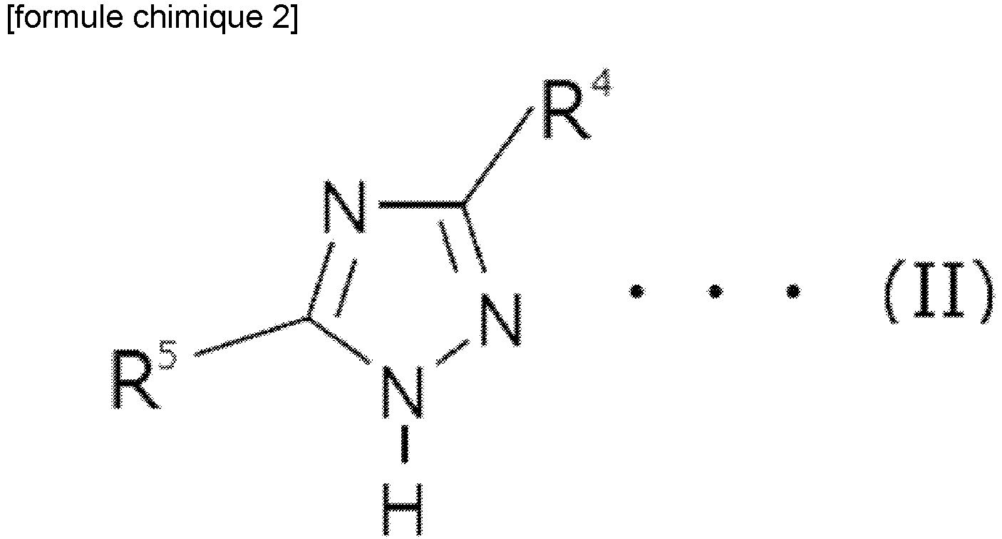
ou représenté par la formule (III) suivante :

- Composition de résine durcissable selon la revendication 1, dans laquelle la proportion de la teneur du composé amine tertiaire dans le total de la teneur du composé triazole (B) et de la teneur du composé amine tertiaire (C) est de 20 % en masse à 80 % en masse.
- Composition de résine durcissable selon l'une quelconque des revendications 1 et 2, comprenant en outre un composé ester actif.
- Composition de résine durcissable selon l'une quelconque des revendications 1 à 3, comprenant en outre un composé polyphénylène-éther.
- Objet en résine durcissable moulé formé par utilisation de la composition de résine durcissable de l'une quelconque des revendications 1 à 4.
- Objet durci obtenu par durcissement de l'objet en résine durcissable moulé de la revendication 5.
- Objet durci selon la revendication 6, dans lequel la tangente de perte diélectrique à une fréquence de 5 GHz est de 0,010 ou moins, dans lequel la tangente de perte diélectrique est mesurée par utilisation d'un procédé de perturbation avec un résonateur à cavité.
- Produit stratifié obtenu par stratification de l'objet durci de la revendication 6 ou 7 et d'un matériau de base.
- Composite comprenant :le produit stratifié de la revendication 8 ; etune couche de conducteur formée sur la surface du côté objet durci du produit stratifié.
- Carte de circuit imprimé multicouche formée par utilisation du composite de la revendication 9.
Applications Claiming Priority (2)
| Application Number | Priority Date | Filing Date | Title |
|---|---|---|---|
| JP2014244349 | 2014-12-02 | ||
| PCT/JP2015/005956 WO2016088358A1 (fr) | 2014-12-02 | 2015-11-30 | Composition de résine durcissable, objet moulé en résine durcissable, objet durci, produit stratifié, composite et carte à circuit imprimé multicouche |
Publications (3)
| Publication Number | Publication Date |
|---|---|
| EP3241857A1 EP3241857A1 (fr) | 2017-11-08 |
| EP3241857A4 EP3241857A4 (fr) | 2018-11-07 |
| EP3241857B1 true EP3241857B1 (fr) | 2020-05-06 |
Family
ID=56091320
Family Applications (1)
| Application Number | Title | Priority Date | Filing Date |
|---|---|---|---|
| EP15865344.4A Active EP3241857B1 (fr) | 2014-12-02 | 2015-11-30 | Composition de résine durcissable, objet moulé en résine durcissable, objet durci, produit stratifié, composite et carte à circuit imprimé multicouche |
Country Status (6)
| Country | Link |
|---|---|
| US (1) | US20180117891A1 (fr) |
| EP (1) | EP3241857B1 (fr) |
| JP (1) | JP6711762B2 (fr) |
| CN (1) | CN107406578B (fr) |
| TW (1) | TWI686443B (fr) |
| WO (1) | WO2016088358A1 (fr) |
Families Citing this family (2)
| Publication number | Priority date | Publication date | Assignee | Title |
|---|---|---|---|---|
| JP7076263B2 (ja) * | 2018-03-30 | 2022-05-27 | 太陽インキ製造株式会社 | 硬化性樹脂組成物、ドライフィルム、硬化物、および、電子部品 |
| JP7333737B2 (ja) * | 2019-09-30 | 2023-08-25 | 太陽ホールディングス株式会社 | 硬化性樹脂組成物、ドライフィルム、樹脂付き銅箔、硬化物、及び電子部品 |
Family Cites Families (11)
| Publication number | Priority date | Publication date | Assignee | Title |
|---|---|---|---|---|
| JPS5360757A (en) * | 1976-11-12 | 1978-05-31 | Sharp Corp | Corrugated heat exchanger |
| JPS63289014A (ja) * | 1987-05-21 | 1988-11-25 | Tamura Kaken Kk | 感光性皮膜組成物 |
| JP3612594B2 (ja) * | 1998-05-29 | 2005-01-19 | 三井金属鉱業株式会社 | 樹脂付複合箔およびその製造方法並びに該複合箔を用いた多層銅張り積層板および多層プリント配線板の製造方法 |
| JP2002110595A (ja) * | 2000-09-29 | 2002-04-12 | Hitachi Ltd | 配線形成方法、研磨方法及び半導体装置の製造方法 |
| JP3977582B2 (ja) * | 2000-09-29 | 2007-09-19 | 和光純薬工業株式会社 | 銅防食剤及び防食方法 |
| JP4364252B2 (ja) * | 2007-04-02 | 2009-11-11 | メック株式会社 | 基板の製造方法及びこれに用いる銅表面処理剤 |
| JP5202052B2 (ja) * | 2008-03-14 | 2013-06-05 | 旭化成株式会社 | 複合材料 |
| JP2009287080A (ja) * | 2008-05-28 | 2009-12-10 | Jfe Steel Corp | 高耐食性表面処理鋼板 |
| JP6091042B2 (ja) * | 2009-06-29 | 2017-03-08 | Jxエネルギー株式会社 | さび止め油組成物 |
| EP2655516B1 (fr) * | 2010-12-26 | 2018-12-26 | Dow Global Technologies LLC | Colles d'assemblage à base de résine époxy, contenant des durcisseurs élastomères à chaînes allongées et coiffés par des composés de phénol, de polyphénol ou d'aminophénol |
| DE102012219479B4 (de) * | 2012-10-24 | 2016-12-15 | Hilti Aktiengesellschaft | Reaktionsharz-Zusammensetzung und deren Verwendung |
-
2015
- 2015-11-30 US US15/532,999 patent/US20180117891A1/en not_active Abandoned
- 2015-11-30 EP EP15865344.4A patent/EP3241857B1/fr active Active
- 2015-11-30 CN CN201580075190.6A patent/CN107406578B/zh active Active
- 2015-11-30 JP JP2016562300A patent/JP6711762B2/ja active Active
- 2015-11-30 WO PCT/JP2015/005956 patent/WO2016088358A1/fr active Application Filing
- 2015-12-02 TW TW104140271A patent/TWI686443B/zh active
Non-Patent Citations (1)
| Title |
|---|
| None * |
Also Published As
| Publication number | Publication date |
|---|---|
| EP3241857A1 (fr) | 2017-11-08 |
| CN107406578B (zh) | 2020-12-01 |
| EP3241857A4 (fr) | 2018-11-07 |
| JPWO2016088358A1 (ja) | 2017-11-02 |
| TW201627392A (zh) | 2016-08-01 |
| WO2016088358A1 (fr) | 2016-06-09 |
| CN107406578A (zh) | 2017-11-28 |
| JP6711762B2 (ja) | 2020-06-17 |
| TWI686443B (zh) | 2020-03-01 |
| US20180117891A1 (en) | 2018-05-03 |
Similar Documents
| Publication | Publication Date | Title |
|---|---|---|
| EP2412743B1 (fr) | Composition de résine thermodurcissable, et pré-imprégné, film d'isolation sur support, plaque stratifiée, et carte de circuit imprimé obtenus à partir de celle-ci | |
| US10544305B2 (en) | Thermosetting resin composition, resin film for interlayer insulation, composite film, printed wiring board, and method for producing same | |
| EP3006503B1 (fr) | Composition de résine pour carte de circuit imprimé ainsi que pré-imprégné mettant en uvre celle-ci, feuille de résine, plaque stratifiée revêtue d'une feuille de métal, et carte de circuit imprimé | |
| KR101386373B1 (ko) | 수지 조성물, 기재부착 절연 시트, 프리프레그, 다층 프린트 배선판 및 반도체 장치 | |
| KR20100095378A (ko) | 수지 조성물 | |
| US11331888B2 (en) | Composite film for electronic devices using high frequency band signals, printed wiring board and manufacturing method therefor | |
| KR20030034106A (ko) | 에폭시 수지 조성물 및 그의 경화물 | |
| JP6357697B2 (ja) | 硬化性エポキシ組成物、フィルム、積層フィルム、プリプレグ、積層体、硬化物、及び複合体 | |
| EP3241857B1 (fr) | Composition de résine durcissable, objet moulé en résine durcissable, objet durci, produit stratifié, composite et carte à circuit imprimé multicouche | |
| TW201441299A (zh) | 硬化性樹脂組成物、絕緣薄膜、預浸材料、硬化物、複合體以及電子材料用基板 | |
| JP2014133877A (ja) | 硬化性樹脂組成物及び硬化物 | |
| EP3428215B1 (fr) | Composition de résine thermodurcissable, son procédé de production, préimprégné, stratifié et carte de circuit imprimé | |
| JP6351062B2 (ja) | 硬化性エポキシ組成物、フィルム、積層フィルム、プリプレグ、積層体、硬化物、及び複合体 | |
| US20180355184A1 (en) | Curable resin composition, curable resin molded article, cured product, laminate, complex, and multi-layer printed circuit board | |
| KR20150133704A (ko) | 경화성 에폭시 조성물, 필름, 적층 필름, 프리프레그, 적층체, 경화물 및 복합체 | |
| EP3541152B1 (fr) | Carte de circuit imprimé et boîter de semi-conducteur | |
| JP6436173B2 (ja) | 硬化性エポキシ組成物、並びに、これを用いて得られるフィルム、積層フィルム、プリプレグ、積層体、硬化物、及び複合体 | |
| WO2019189783A1 (fr) | Stratifié, plaque stratifiée comprenant une couche conductrice, carte de circuit imprimé, procédés de production associés et boîtier de semi-conducteur | |
| TWI715555B (zh) | 硬化性樹脂組合物、硬化性樹脂成形體、硬化物、積層體、複合物以及多層印刷配線板 | |
| KR102603150B1 (ko) | 층간 절연용 수지 필름, 접착 보조층 구비 층간 절연용 수지 필름 및 프린트 배선판 | |
| WO2016067329A1 (fr) | Composition époxy durcissable, film, film stratifié, préimprégné, corps stratifié, matériau durci, et composite |
Legal Events
| Date | Code | Title | Description |
|---|---|---|---|
| STAA | Information on the status of an ep patent application or granted ep patent |
Free format text: STATUS: THE INTERNATIONAL PUBLICATION HAS BEEN MADE |
|
| PUAI | Public reference made under article 153(3) epc to a published international application that has entered the european phase |
Free format text: ORIGINAL CODE: 0009012 |
|
| STAA | Information on the status of an ep patent application or granted ep patent |
Free format text: STATUS: REQUEST FOR EXAMINATION WAS MADE |
|
| 17P | Request for examination filed |
Effective date: 20170703 |
|
| AK | Designated contracting states |
Kind code of ref document: A1 Designated state(s): AL AT BE BG CH CY CZ DE DK EE ES FI FR GB GR HR HU IE IS IT LI LT LU LV MC MK MT NL NO PL PT RO RS SE SI SK SM TR |
|
| AX | Request for extension of the european patent |
Extension state: BA ME |
|
| DAV | Request for validation of the european patent (deleted) | ||
| DAX | Request for extension of the european patent (deleted) | ||
| RIC1 | Information provided on ipc code assigned before grant |
Ipc: B32B 7/02 20060101ALI20180816BHEP Ipc: C08L 63/00 20060101ALI20180816BHEP Ipc: H05K 1/03 20060101ALI20180816BHEP Ipc: C08L 71/12 20060101ALI20180816BHEP Ipc: C08G 59/50 20060101ALI20180816BHEP Ipc: C08K 5/17 20060101ALI20180816BHEP Ipc: C08G 59/40 20060101AFI20180816BHEP Ipc: B32B 27/38 20060101ALI20180816BHEP Ipc: C08K 5/3472 20060101ALI20180816BHEP |
|
| RIC1 | Information provided on ipc code assigned before grant |
Ipc: C08K 5/17 20060101ALI20180911BHEP Ipc: C08L 63/00 20060101ALI20180911BHEP Ipc: C08L 71/12 20060101ALI20180911BHEP Ipc: H05K 1/03 20060101ALI20180911BHEP Ipc: B32B 7/02 20060101ALI20180911BHEP Ipc: B32B 27/38 20060101ALI20180911BHEP Ipc: C08G 59/40 20060101AFI20180911BHEP Ipc: C08K 5/3472 20060101ALI20180911BHEP Ipc: C08G 59/50 20060101ALI20180911BHEP |
|
| A4 | Supplementary search report drawn up and despatched |
Effective date: 20181005 |
|
| RIC1 | Information provided on ipc code assigned before grant |
Ipc: C08K 5/17 20060101ALI20181003BHEP Ipc: C08L 71/12 20060101ALI20181003BHEP Ipc: C08G 59/50 20060101ALI20181003BHEP Ipc: C08G 59/40 20060101AFI20181003BHEP Ipc: B32B 27/38 20060101ALI20181003BHEP Ipc: C08K 5/3472 20060101ALI20181003BHEP Ipc: B32B 7/02 20060101ALI20181003BHEP Ipc: H05K 1/03 20060101ALI20181003BHEP Ipc: C08L 63/00 20060101ALI20181003BHEP |
|
| GRAP | Despatch of communication of intention to grant a patent |
Free format text: ORIGINAL CODE: EPIDOSNIGR1 |
|
| STAA | Information on the status of an ep patent application or granted ep patent |
Free format text: STATUS: GRANT OF PATENT IS INTENDED |
|
| RIC1 | Information provided on ipc code assigned before grant |
Ipc: C08G 59/50 20060101ALI20191122BHEP Ipc: C09J 163/00 20060101ALI20191122BHEP Ipc: C08L 71/12 20060101ALI20191122BHEP Ipc: C08L 63/00 20060101ALI20191122BHEP Ipc: B32B 7/02 20190101ALI20191122BHEP Ipc: H05K 1/03 20060101ALI20191122BHEP Ipc: C08K 5/3472 20060101ALI20191122BHEP Ipc: B32B 27/38 20060101ALI20191122BHEP Ipc: C08K 5/17 20060101ALI20191122BHEP Ipc: C08G 59/40 20060101AFI20191122BHEP Ipc: C08G 59/68 20060101ALI20191122BHEP |
|
| INTG | Intention to grant announced |
Effective date: 20191212 |
|
| GRAS | Grant fee paid |
Free format text: ORIGINAL CODE: EPIDOSNIGR3 |
|
| GRAA | (expected) grant |
Free format text: ORIGINAL CODE: 0009210 |
|
| STAA | Information on the status of an ep patent application or granted ep patent |
Free format text: STATUS: THE PATENT HAS BEEN GRANTED |
|
| AK | Designated contracting states |
Kind code of ref document: B1 Designated state(s): AL AT BE BG CH CY CZ DE DK EE ES FI FR GB GR HR HU IE IS IT LI LT LU LV MC MK MT NL NO PL PT RO RS SE SI SK SM TR |
|
| REG | Reference to a national code |
Ref country code: GB Ref legal event code: FG4D |
|
| REG | Reference to a national code |
Ref country code: CH Ref legal event code: EP Ref country code: AT Ref legal event code: REF Ref document number: 1266618 Country of ref document: AT Kind code of ref document: T Effective date: 20200515 |
|
| REG | Reference to a national code |
Ref country code: IE Ref legal event code: FG4D |
|
| REG | Reference to a national code |
Ref country code: DE Ref legal event code: R096 Ref document number: 602015052531 Country of ref document: DE |
|
| REG | Reference to a national code |
Ref country code: NL Ref legal event code: FP |
|
| REG | Reference to a national code |
Ref country code: LT Ref legal event code: MG4D |
|
| PG25 | Lapsed in a contracting state [announced via postgrant information from national office to epo] |
Ref country code: PT Free format text: LAPSE BECAUSE OF FAILURE TO SUBMIT A TRANSLATION OF THE DESCRIPTION OR TO PAY THE FEE WITHIN THE PRESCRIBED TIME-LIMIT Effective date: 20200907 Ref country code: FI Free format text: LAPSE BECAUSE OF FAILURE TO SUBMIT A TRANSLATION OF THE DESCRIPTION OR TO PAY THE FEE WITHIN THE PRESCRIBED TIME-LIMIT Effective date: 20200506 Ref country code: NO Free format text: LAPSE BECAUSE OF FAILURE TO SUBMIT A TRANSLATION OF THE DESCRIPTION OR TO PAY THE FEE WITHIN THE PRESCRIBED TIME-LIMIT Effective date: 20200806 Ref country code: LT Free format text: LAPSE BECAUSE OF FAILURE TO SUBMIT A TRANSLATION OF THE DESCRIPTION OR TO PAY THE FEE WITHIN THE PRESCRIBED TIME-LIMIT Effective date: 20200506 Ref country code: IS Free format text: LAPSE BECAUSE OF FAILURE TO SUBMIT A TRANSLATION OF THE DESCRIPTION OR TO PAY THE FEE WITHIN THE PRESCRIBED TIME-LIMIT Effective date: 20200906 Ref country code: SE Free format text: LAPSE BECAUSE OF FAILURE TO SUBMIT A TRANSLATION OF THE DESCRIPTION OR TO PAY THE FEE WITHIN THE PRESCRIBED TIME-LIMIT Effective date: 20200506 Ref country code: GR Free format text: LAPSE BECAUSE OF FAILURE TO SUBMIT A TRANSLATION OF THE DESCRIPTION OR TO PAY THE FEE WITHIN THE PRESCRIBED TIME-LIMIT Effective date: 20200807 |
|
| PG25 | Lapsed in a contracting state [announced via postgrant information from national office to epo] |
Ref country code: BG Free format text: LAPSE BECAUSE OF FAILURE TO SUBMIT A TRANSLATION OF THE DESCRIPTION OR TO PAY THE FEE WITHIN THE PRESCRIBED TIME-LIMIT Effective date: 20200806 Ref country code: RS Free format text: LAPSE BECAUSE OF FAILURE TO SUBMIT A TRANSLATION OF THE DESCRIPTION OR TO PAY THE FEE WITHIN THE PRESCRIBED TIME-LIMIT Effective date: 20200506 Ref country code: LV Free format text: LAPSE BECAUSE OF FAILURE TO SUBMIT A TRANSLATION OF THE DESCRIPTION OR TO PAY THE FEE WITHIN THE PRESCRIBED TIME-LIMIT Effective date: 20200506 Ref country code: HR Free format text: LAPSE BECAUSE OF FAILURE TO SUBMIT A TRANSLATION OF THE DESCRIPTION OR TO PAY THE FEE WITHIN THE PRESCRIBED TIME-LIMIT Effective date: 20200506 |
|
| REG | Reference to a national code |
Ref country code: AT Ref legal event code: MK05 Ref document number: 1266618 Country of ref document: AT Kind code of ref document: T Effective date: 20200506 |
|
| REG | Reference to a national code |
Ref country code: DE Ref legal event code: R082 Ref document number: 602015052531 Country of ref document: DE Ref country code: DE Ref legal event code: R081 Ref document number: 602015052531 Country of ref document: DE Owner name: INTEL CORPORATION, SANTA CLARA, US Free format text: FORMER OWNER: ZEON CORPORATION, TOKYO, JP |
|
| PG25 | Lapsed in a contracting state [announced via postgrant information from national office to epo] |
Ref country code: AL Free format text: LAPSE BECAUSE OF FAILURE TO SUBMIT A TRANSLATION OF THE DESCRIPTION OR TO PAY THE FEE WITHIN THE PRESCRIBED TIME-LIMIT Effective date: 20200506 |
|
| REG | Reference to a national code |
Ref country code: GB Ref legal event code: 732E Free format text: REGISTERED BETWEEN 20201224 AND 20201230 |
|
| PG25 | Lapsed in a contracting state [announced via postgrant information from national office to epo] |
Ref country code: IT Free format text: LAPSE BECAUSE OF FAILURE TO SUBMIT A TRANSLATION OF THE DESCRIPTION OR TO PAY THE FEE WITHIN THE PRESCRIBED TIME-LIMIT Effective date: 20200506 Ref country code: SM Free format text: LAPSE BECAUSE OF FAILURE TO SUBMIT A TRANSLATION OF THE DESCRIPTION OR TO PAY THE FEE WITHIN THE PRESCRIBED TIME-LIMIT Effective date: 20200506 Ref country code: EE Free format text: LAPSE BECAUSE OF FAILURE TO SUBMIT A TRANSLATION OF THE DESCRIPTION OR TO PAY THE FEE WITHIN THE PRESCRIBED TIME-LIMIT Effective date: 20200506 Ref country code: CZ Free format text: LAPSE BECAUSE OF FAILURE TO SUBMIT A TRANSLATION OF THE DESCRIPTION OR TO PAY THE FEE WITHIN THE PRESCRIBED TIME-LIMIT Effective date: 20200506 Ref country code: AT Free format text: LAPSE BECAUSE OF FAILURE TO SUBMIT A TRANSLATION OF THE DESCRIPTION OR TO PAY THE FEE WITHIN THE PRESCRIBED TIME-LIMIT Effective date: 20200506 Ref country code: RO Free format text: LAPSE BECAUSE OF FAILURE TO SUBMIT A TRANSLATION OF THE DESCRIPTION OR TO PAY THE FEE WITHIN THE PRESCRIBED TIME-LIMIT Effective date: 20200506 Ref country code: ES Free format text: LAPSE BECAUSE OF FAILURE TO SUBMIT A TRANSLATION OF THE DESCRIPTION OR TO PAY THE FEE WITHIN THE PRESCRIBED TIME-LIMIT Effective date: 20200506 Ref country code: DK Free format text: LAPSE BECAUSE OF FAILURE TO SUBMIT A TRANSLATION OF THE DESCRIPTION OR TO PAY THE FEE WITHIN THE PRESCRIBED TIME-LIMIT Effective date: 20200506 |
|
| REG | Reference to a national code |
Ref country code: DE Ref legal event code: R097 Ref document number: 602015052531 Country of ref document: DE |
|
| PG25 | Lapsed in a contracting state [announced via postgrant information from national office to epo] |
Ref country code: PL Free format text: LAPSE BECAUSE OF FAILURE TO SUBMIT A TRANSLATION OF THE DESCRIPTION OR TO PAY THE FEE WITHIN THE PRESCRIBED TIME-LIMIT Effective date: 20200506 Ref country code: SK Free format text: LAPSE BECAUSE OF FAILURE TO SUBMIT A TRANSLATION OF THE DESCRIPTION OR TO PAY THE FEE WITHIN THE PRESCRIBED TIME-LIMIT Effective date: 20200506 |
|
| PLBE | No opposition filed within time limit |
Free format text: ORIGINAL CODE: 0009261 |
|
| STAA | Information on the status of an ep patent application or granted ep patent |
Free format text: STATUS: NO OPPOSITION FILED WITHIN TIME LIMIT |
|
| 26N | No opposition filed |
Effective date: 20210209 |
|
| PG25 | Lapsed in a contracting state [announced via postgrant information from national office to epo] |
Ref country code: SI Free format text: LAPSE BECAUSE OF FAILURE TO SUBMIT A TRANSLATION OF THE DESCRIPTION OR TO PAY THE FEE WITHIN THE PRESCRIBED TIME-LIMIT Effective date: 20200506 |
|
| PG25 | Lapsed in a contracting state [announced via postgrant information from national office to epo] |
Ref country code: MC Free format text: LAPSE BECAUSE OF FAILURE TO SUBMIT A TRANSLATION OF THE DESCRIPTION OR TO PAY THE FEE WITHIN THE PRESCRIBED TIME-LIMIT Effective date: 20200506 |
|
| REG | Reference to a national code |
Ref country code: CH Ref legal event code: PL |
|
| PG25 | Lapsed in a contracting state [announced via postgrant information from national office to epo] |
Ref country code: LU Free format text: LAPSE BECAUSE OF NON-PAYMENT OF DUE FEES Effective date: 20201130 |
|
| REG | Reference to a national code |
Ref country code: BE Ref legal event code: MM Effective date: 20201130 |
|
| PG25 | Lapsed in a contracting state [announced via postgrant information from national office to epo] |
Ref country code: LI Free format text: LAPSE BECAUSE OF NON-PAYMENT OF DUE FEES Effective date: 20201130 Ref country code: CH Free format text: LAPSE BECAUSE OF NON-PAYMENT OF DUE FEES Effective date: 20201130 |
|
| REG | Reference to a national code |
Ref country code: IE Ref legal event code: MM4A |
|
| PG25 | Lapsed in a contracting state [announced via postgrant information from national office to epo] |
Ref country code: IE Free format text: LAPSE BECAUSE OF NON-PAYMENT OF DUE FEES Effective date: 20201130 |
|
| PG25 | Lapsed in a contracting state [announced via postgrant information from national office to epo] |
Ref country code: TR Free format text: LAPSE BECAUSE OF FAILURE TO SUBMIT A TRANSLATION OF THE DESCRIPTION OR TO PAY THE FEE WITHIN THE PRESCRIBED TIME-LIMIT Effective date: 20200506 Ref country code: MT Free format text: LAPSE BECAUSE OF FAILURE TO SUBMIT A TRANSLATION OF THE DESCRIPTION OR TO PAY THE FEE WITHIN THE PRESCRIBED TIME-LIMIT Effective date: 20200506 Ref country code: CY Free format text: LAPSE BECAUSE OF FAILURE TO SUBMIT A TRANSLATION OF THE DESCRIPTION OR TO PAY THE FEE WITHIN THE PRESCRIBED TIME-LIMIT Effective date: 20200506 |
|
| PG25 | Lapsed in a contracting state [announced via postgrant information from national office to epo] |
Ref country code: MK Free format text: LAPSE BECAUSE OF FAILURE TO SUBMIT A TRANSLATION OF THE DESCRIPTION OR TO PAY THE FEE WITHIN THE PRESCRIBED TIME-LIMIT Effective date: 20200506 |
|
| PG25 | Lapsed in a contracting state [announced via postgrant information from national office to epo] |
Ref country code: BE Free format text: LAPSE BECAUSE OF NON-PAYMENT OF DUE FEES Effective date: 20201130 |
|
| P01 | Opt-out of the competence of the unified patent court (upc) registered |
Effective date: 20230518 |
|
| PGFP | Annual fee paid to national office [announced via postgrant information from national office to epo] |
Ref country code: NL Payment date: 20230925 Year of fee payment: 9 Ref country code: GB Payment date: 20230914 Year of fee payment: 9 |
|
| PGFP | Annual fee paid to national office [announced via postgrant information from national office to epo] |
Ref country code: FR Payment date: 20230921 Year of fee payment: 9 |
|
| PGFP | Annual fee paid to national office [announced via postgrant information from national office to epo] |
Ref country code: DE Payment date: 20230919 Year of fee payment: 9 |