EP3228583A1 - Procédé de production de microstructure de microsystème électromécanique suspendue à double couche et détecteur infrarouge à microsystème électromécanique - Google Patents
Procédé de production de microstructure de microsystème électromécanique suspendue à double couche et détecteur infrarouge à microsystème électromécanique Download PDFInfo
- Publication number
- EP3228583A1 EP3228583A1 EP15866031.6A EP15866031A EP3228583A1 EP 3228583 A1 EP3228583 A1 EP 3228583A1 EP 15866031 A EP15866031 A EP 15866031A EP 3228583 A1 EP3228583 A1 EP 3228583A1
- Authority
- EP
- European Patent Office
- Prior art keywords
- film body
- layer
- sacrificial layer
- substrate
- dielectric layer
- Prior art date
- Legal status (The legal status is an assumption and is not a legal conclusion. Google has not performed a legal analysis and makes no representation as to the accuracy of the status listed.)
- Granted
Links
- 239000000725 suspension Substances 0.000 title claims abstract description 54
- 238000004519 manufacturing process Methods 0.000 title claims abstract description 37
- 238000000034 method Methods 0.000 title claims abstract description 21
- 239000000758 substrate Substances 0.000 claims abstract description 41
- 238000000059 patterning Methods 0.000 claims abstract description 15
- 238000000151 deposition Methods 0.000 claims abstract description 7
- 239000004642 Polyimide Substances 0.000 claims description 28
- 229920001721 polyimide Polymers 0.000 claims description 28
- 239000000463 material Substances 0.000 claims description 15
- VYPSYNLAJGMNEJ-UHFFFAOYSA-N Silicium dioxide Chemical compound O=[Si]=O VYPSYNLAJGMNEJ-UHFFFAOYSA-N 0.000 claims description 14
- 239000001301 oxygen Substances 0.000 claims description 9
- 229910052760 oxygen Inorganic materials 0.000 claims description 9
- 229910052581 Si3N4 Inorganic materials 0.000 claims description 7
- XUIMIQQOPSSXEZ-UHFFFAOYSA-N Silicon Chemical compound [Si] XUIMIQQOPSSXEZ-UHFFFAOYSA-N 0.000 claims description 7
- 229910052710 silicon Inorganic materials 0.000 claims description 7
- 239000010703 silicon Substances 0.000 claims description 7
- 235000012239 silicon dioxide Nutrition 0.000 claims description 7
- 239000000377 silicon dioxide Substances 0.000 claims description 7
- HQVNEWCFYHHQES-UHFFFAOYSA-N silicon nitride Chemical compound N12[Si]34N5[Si]62N3[Si]51N64 HQVNEWCFYHHQES-UHFFFAOYSA-N 0.000 claims description 7
- 238000001312 dry etching Methods 0.000 claims description 5
- 239000010410 layer Substances 0.000 description 114
- 239000002356 single layer Substances 0.000 description 16
- 230000005855 radiation Effects 0.000 description 7
- QVGXLLKOCUKJST-UHFFFAOYSA-N atomic oxygen Chemical compound [O] QVGXLLKOCUKJST-UHFFFAOYSA-N 0.000 description 4
- 238000005530 etching Methods 0.000 description 4
- 239000004065 semiconductor Substances 0.000 description 3
- 239000011248 coating agent Substances 0.000 description 2
- 238000000576 coating method Methods 0.000 description 2
- 230000005616 pyroelectricity Effects 0.000 description 2
- 230000005678 Seebeck effect Effects 0.000 description 1
- 238000010521 absorption reaction Methods 0.000 description 1
- 238000009825 accumulation Methods 0.000 description 1
- 239000007789 gas Substances 0.000 description 1
- 230000002093 peripheral effect Effects 0.000 description 1
Images

Classifications
-
- B—PERFORMING OPERATIONS; TRANSPORTING
- B81—MICROSTRUCTURAL TECHNOLOGY
- B81B—MICROSTRUCTURAL DEVICES OR SYSTEMS, e.g. MICROMECHANICAL DEVICES
- B81B7/00—Microstructural systems; Auxiliary parts of microstructural devices or systems
- B81B7/02—Microstructural systems; Auxiliary parts of microstructural devices or systems containing distinct electrical or optical devices of particular relevance for their function, e.g. microelectro-mechanical systems [MEMS]
-
- B—PERFORMING OPERATIONS; TRANSPORTING
- B81—MICROSTRUCTURAL TECHNOLOGY
- B81C—PROCESSES OR APPARATUS SPECIALLY ADAPTED FOR THE MANUFACTURE OR TREATMENT OF MICROSTRUCTURAL DEVICES OR SYSTEMS
- B81C1/00—Manufacture or treatment of devices or systems in or on a substrate
- B81C1/00015—Manufacture or treatment of devices or systems in or on a substrate for manufacturing microsystems
- B81C1/00134—Manufacture or treatment of devices or systems in or on a substrate for manufacturing microsystems comprising flexible or deformable structures
- B81C1/0015—Cantilevers
-
- B—PERFORMING OPERATIONS; TRANSPORTING
- B81—MICROSTRUCTURAL TECHNOLOGY
- B81C—PROCESSES OR APPARATUS SPECIALLY ADAPTED FOR THE MANUFACTURE OR TREATMENT OF MICROSTRUCTURAL DEVICES OR SYSTEMS
- B81C1/00—Manufacture or treatment of devices or systems in or on a substrate
-
- G—PHYSICS
- G01—MEASURING; TESTING
- G01J—MEASUREMENT OF INTENSITY, VELOCITY, SPECTRAL CONTENT, POLARISATION, PHASE OR PULSE CHARACTERISTICS OF INFRARED, VISIBLE OR ULTRAVIOLET LIGHT; COLORIMETRY; RADIATION PYROMETRY
- G01J1/00—Photometry, e.g. photographic exposure meter
- G01J1/02—Details
- G01J1/04—Optical or mechanical part supplementary adjustable parts
-
- G—PHYSICS
- G01—MEASURING; TESTING
- G01J—MEASUREMENT OF INTENSITY, VELOCITY, SPECTRAL CONTENT, POLARISATION, PHASE OR PULSE CHARACTERISTICS OF INFRARED, VISIBLE OR ULTRAVIOLET LIGHT; COLORIMETRY; RADIATION PYROMETRY
- G01J1/00—Photometry, e.g. photographic exposure meter
- G01J1/42—Photometry, e.g. photographic exposure meter using electric radiation detectors
-
- G—PHYSICS
- G01—MEASURING; TESTING
- G01J—MEASUREMENT OF INTENSITY, VELOCITY, SPECTRAL CONTENT, POLARISATION, PHASE OR PULSE CHARACTERISTICS OF INFRARED, VISIBLE OR ULTRAVIOLET LIGHT; COLORIMETRY; RADIATION PYROMETRY
- G01J5/00—Radiation pyrometry, e.g. infrared or optical thermometry
- G01J5/02—Constructional details
- G01J5/0225—Shape of the cavity itself or of elements contained in or suspended over the cavity
- G01J5/024—Special manufacturing steps or sacrificial layers or layer structures
-
- G—PHYSICS
- G01—MEASURING; TESTING
- G01J—MEASUREMENT OF INTENSITY, VELOCITY, SPECTRAL CONTENT, POLARISATION, PHASE OR PULSE CHARACTERISTICS OF INFRARED, VISIBLE OR ULTRAVIOLET LIGHT; COLORIMETRY; RADIATION PYROMETRY
- G01J5/00—Radiation pyrometry, e.g. infrared or optical thermometry
- G01J5/02—Constructional details
- G01J5/08—Optical arrangements
- G01J5/0853—Optical arrangements having infrared absorbers other than the usual absorber layers deposited on infrared detectors like bolometers, wherein the heat propagation between the absorber and the detecting element occurs within a solid
-
- B—PERFORMING OPERATIONS; TRANSPORTING
- B81—MICROSTRUCTURAL TECHNOLOGY
- B81B—MICROSTRUCTURAL DEVICES OR SYSTEMS, e.g. MICROMECHANICAL DEVICES
- B81B2201/00—Specific applications of microelectromechanical systems
- B81B2201/02—Sensors
- B81B2201/0278—Temperature sensors
-
- B—PERFORMING OPERATIONS; TRANSPORTING
- B81—MICROSTRUCTURAL TECHNOLOGY
- B81B—MICROSTRUCTURAL DEVICES OR SYSTEMS, e.g. MICROMECHANICAL DEVICES
- B81B2203/00—Basic microelectromechanical structures
- B81B2203/01—Suspended structures, i.e. structures allowing a movement
- B81B2203/0118—Cantilevers
-
- B—PERFORMING OPERATIONS; TRANSPORTING
- B81—MICROSTRUCTURAL TECHNOLOGY
- B81C—PROCESSES OR APPARATUS SPECIALLY ADAPTED FOR THE MANUFACTURE OR TREATMENT OF MICROSTRUCTURAL DEVICES OR SYSTEMS
- B81C2201/00—Manufacture or treatment of microstructural devices or systems
- B81C2201/01—Manufacture or treatment of microstructural devices or systems in or on a substrate
- B81C2201/0174—Manufacture or treatment of microstructural devices or systems in or on a substrate for making multi-layered devices, film deposition or growing
- B81C2201/0197—Processes for making multi-layered devices not provided for in groups B81C2201/0176 - B81C2201/0192
Definitions
- the invention relates to semiconductors, and more particular, relates to a method of manufacturing a MEMS double-layer suspension microstructure and a MEMS infrared detector.
- MEMS Micro Electro Mechanical Systems
- the infrared detector manufactured by using a MEMS technology possesses significant advantages at aspects such as the volume, power consumption, weight, and cost.
- the infrared detector manufactured by using a MEMS technology is extensively applied to military fair and civil field. According to a difference of working principle, the infrared detector mainly includes a thermo-electric pile detector, a pyroelectricity detector and a thermo-sensitive resistance detector.
- thermo-electric pile detector takes advantage of Seebeck effect to transfer a temperature variation caused by an infrared radiation into a voltage signal output.
- the pyroelectricity infrared detector takes advantage of charge accumulation in a heated body to detect a temperature variation caused by an infrared radiation.
- the thermo-sensitive resistance infrared detector takes advantage of reading a resistance value to detect a temperature variation caused by an infrared radiation.
- MEMS infrared detector generally adopts a single-layer suspension microstructure, the technology is simple. However, when a size of the infrared detector chip is reduced, the suspension absorbing region (a film-like absorb layer) servings for absorbing the infrared radiation is reduced at the same time, thus the infrared response rate is reduced greatly.
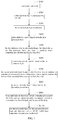
- a method of manufacturing a MEMS double-layer suspension microstructure includes the steps: providing a substrate; forming a first sacrificial layer on the substrate; patterning the first sacrificial layer; depositing a first dielectric layer on the first sacrificial layer; patterning the first dielectric layer to form a first film body on the first sacrificial layer, and a cantilever beam connecting the substrate and the first film body; forming a second sacrificial layer on the first dielectric layer; patterning the second sacrificial layer located on the first film body to manufacture a recessed portion configured to form a support structure, a bottom of the recessed portion exposing the first film body; depositing a second dielectric layer on the second sacrificial layer; patterning the second dielectric layer to manufacture a second film body and the support structure, the support structure connecting the first film body and the second film body; and removing the first sacrificial layer and the second sacrificial layer to obtain a MEMS double-layer suspension microstructure
- Another method of manufacturing a MEMS double-layer suspension microstructure includes the steps: forming a first film body on a substrate, and forming a cantilever beam connecting the substrate and the first film body; forming a sacrificial layer on the first film body and the cantilever beam; patterning the sacrificial layer located on the first film body to manufacture a recessed portion configured to form a support structure, a bottom of the recessed portion exposing the first film body; depositing a dielectric layer on the sacrificial layer; patterning the dielectric layer to manufacture a second film body and the support structure, the support structure connecting the first film body and the second film body; and removing the sacrificial layer to obtain a MEMS double-layer suspension microstructure.
- a MEMS infrared detector includes a MEMS double-layer suspension microstructure, wherein the MEMS double-layer suspension microstructure includes: a substrate; a first film body on the substrate; a cantilever beam connecting the substrate and the first film body; a second film body on the first film body; and a support structure connecting the first film body and the second film body.
- Above method of manufacturing a MEMS double-layer suspension microstructure can manufacture a double-layer suspension microstructure, the infrared detector manufactured by the double-layer suspension microstructure (the suspension microstructure having a first dielectric layer and a second dielectric layer), because there is no need to manufacture a cantilever beam on the second dielectric layer, thus the second dielectric layer can be manufactured greater than the first dielectric layer, therefore, it possesses a larger suspension absorbing region than that of an infrared detector having a single layer suspension microstructure, thereby an infrared response rate is greatly increased when compared to a conventional infrared detector having a single layer suspension microstructure.
- the infrared detector chip When a size of the infrared detector chip is reduced, compared to a conventional infrared detector having a single layer suspension microstructure, even if the suspension region (the second dielectric layer) used for absorbing infrared radiation can be reduced accordingly, however, because there is no need to manufacture a cantilever beam on the second dielectric layer, thus the second dielectric layer can be manufactured greater than the first dielectric layer, therefore, even if the size of the infrared detector chip is reduced, it can also possess a larger suspension absorbing region than that of the infrared detector having a single layer suspension microstructure, the infrared response rate is greatly increased when compared to the conventional infrared detector having a single layer suspension microstructure.
- FIG. 1 is a flow chart of a method of manufacturing a MEMS double-layer suspension microstructure according to an embodiment.
- the first sacrificial layer and/or the second sacrificial layer are polyimide layers.
- a method of manufacturing a MEMS double-layer suspension microstructure includes steps as follows:
- the single layer suspension microstructure has other well known manufacturing method, thus in alternative embodiments, other methods can also be adopted to form the first film body 310 on the substrate 100, and form the cantilever beam 320 connecting the substrate 100 and the first film body 310.
- a second polyimide layer 400 is formed on the first dielectric layer 400.
- the second polyimide layer 400 is formed by coating, and the second polyimide layer 400 has a thickness ranging from 500 nanometers to 3000 nanometers.
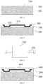
- step S700 the second polyimide layer 400 located on the first film body 310 is patterned to manufacture a recessed portion 410 configured to form a support structure 520, the bottom of the recessed portion 410 exposes the first film body 310.
- the number of the recessed portion 410 is one, the recessed portion 410 is exposed above the first film body 310 and located on a central position of the second polyimide layer 400.
- a second dielectric layer 500 is deposited on the second polyimide layer 400.
- the second dielectric layer 500 has a thickness ranging from 100 nanometers to 2000 nanometers.
- the second dielectric layer 500 is made of silicon dioxide, silicon nitride, silicon oxynitride or a combination of two laminated layers of above materials or a combination of three laminated layers of above materials, i.e. the second dielectric layer 500 can be a single layer structure of silicon dioxide, silicon nitride, or silicon oxynitride, and also can be a non single layer structure of a combination of two laminated layers of above materials or a combination of three laminated layers of above materials.
- the second dielectric layer 500 is patterned to manufacture a second film body 510 and the support structure 520, the support structure 520 is connected to the first film body 310 and the second film body 510.
- the dielectric layer deposited on the recessed portion 410 of the second polyimide layer 400 is patterned and serves as the support structure 520, a peripheral region connected to the support structure 520 forms the second film body 510.
- a projection area of the second film body 510 on the surface of the substrate 100 can be fabricated greater than a projection area of the first film body 310 on the substrate 100.
- the second film body 510 is fixed to the first film body 310 by the second polyimide layer 400.
- step S1100 the first polyimide layer 200 and the second polyimide layer 400 are removed, and a MEMS double-layer suspension microstructure is obtained, referring to FIG. 8 .
- the first polyimide layer 200 and the second polyimide layer 400 are removed by using an oxygen ion dry etching technology, and a MEMS double-layer suspension microstructure is obtained.
- the working principle of the oxygen ion dry etching technology is that, a little oxygen is filled into a vacuum system, and a high voltage is applied to ionize the oxygen, thereby forming a glow column of oxygen plasma.
- the active oxygen can oxidize the polyimide quickly and generates a volatile gaseous, thereby achieving an etching process.
- the first polyimide layer 200 and the second polyimide layer 400 are regarded as sacrificial layers in the method.
- any other material which can be removed by semiconductor etching technology can substitute the sacrificial layer in the method.
- the semiconductor etching technology certainly includes an etching technology adopting gas or light to etch, for example an oxygen ion dry etching technology.
- both the first film body 310 and the second film body 510 (mainly depend on the second film body 510) can be employed to absorb the film-like absorbing layer for absorbing infrared radiation, the electric signal transferred by the absorbed infrared energy is transmitted to the circuit structure of first substrate 100 via the cantilever beam 320.
- the invention further discloses a MEMS infrared detector
- the MEMS double-layer suspension microstructure can be manufactured by above method of manufacturing a MEMS double-layer suspension microstructure.
- the MEMS double-layer microstructure includes a substrate 100, a first film body 310 on the substrate 100, and a cantilever beam 320 connecting the substrate 100 and the first film body 310, a second film body 510 on the first film body 310, and a support structure 520 connecting the first film body 310 and the second film body 510.
- the MEMS infrared detector can be thermo-sensitive resistance infrared detector.
- Above method of manufacturing a MEMS double-layer suspension microstructure can manufacture a double-layer suspension microstructure, the infrared detector manufactured by the double-layer suspension microstructure (the suspension microstructure having a first dielectric layer and a second dielectric layer), because there is no need to manufacture a cantilever beam on the second dielectric layer, thus the second dielectric layer can be manufactured greater than the first dielectric layer, therefore, it possesses a larger suspension absorbing region than that of an infrared detector having a single layer suspension microstructure, thereby an infrared response rate is greatly increased when compared to a conventional infrared detector having a single layer suspension microstructure.
- the infrared detector chip When a size of the infrared detector chip is reduced, compared to a conventional infrared detector having a single layer suspension microstructure, even if the suspension region (the second dielectric layer) used for absorbing infrared radiation can be reduced accordingly, however, because there is no need to manufacture a cantilever beam on the second dielectric layer, thus the second dielectric layer can be manufactured greater than the first dielectric layer, therefore, even if the size of the infrared detector chip is reduced, it can also possess a larger suspension absorbing region than that of the infrared detector having a single layer suspension microstructure, the infrared response rate is greatly increased when compared to the conventional infrared detector having a single layer suspension microstructure.
Applications Claiming Priority (2)
| Application Number | Priority Date | Filing Date | Title |
|---|---|---|---|
| CN201410723696.0A CN105712284B (zh) | 2014-12-02 | 2014-12-02 | Mems双层悬浮微结构的制作方法和mems红外探测器 |
| PCT/CN2015/087594 WO2016086690A1 (fr) | 2014-12-02 | 2015-08-20 | Procédé de production de microstructure de microsystème électromécanique suspendue à double couche et détecteur infrarouge à microsystème électromécanique |
Publications (4)
| Publication Number | Publication Date |
|---|---|
| EP3228583A1 true EP3228583A1 (fr) | 2017-10-11 |
| EP3228583A4 EP3228583A4 (fr) | 2018-07-25 |
| EP3228583C0 EP3228583C0 (fr) | 2023-11-01 |
| EP3228583B1 EP3228583B1 (fr) | 2023-11-01 |
Family
ID=56090957
Family Applications (1)
| Application Number | Title | Priority Date | Filing Date |
|---|---|---|---|
| EP15866031.6A Active EP3228583B1 (fr) | 2014-12-02 | 2015-08-20 | Procédé de production de microstructure de microsystème électromécanique suspendue à double couche et détecteur infrarouge à microsystème électromécanique |
Country Status (5)
| Country | Link |
|---|---|
| US (1) | US10301175B2 (fr) |
| EP (1) | EP3228583B1 (fr) |
| JP (1) | JP2017524126A (fr) |
| CN (1) | CN105712284B (fr) |
| WO (1) | WO2016086690A1 (fr) |
Families Citing this family (2)
| Publication number | Priority date | Publication date | Assignee | Title |
|---|---|---|---|---|
| CN106672891A (zh) * | 2017-01-24 | 2017-05-17 | 烟台睿创微纳技术股份有限公司 | 一种双层非制冷红外探测器结构及其制备方法 |
| CN106629578B (zh) * | 2017-02-15 | 2019-07-12 | 浙江大立科技股份有限公司 | 具有微桥结构的红外探测器及其制造方法 |
Family Cites Families (26)
| Publication number | Priority date | Publication date | Assignee | Title |
|---|---|---|---|---|
| JP3040356B2 (ja) * | 1997-01-27 | 2000-05-15 | 三菱電機株式会社 | 赤外線固体撮像素子 |
| US6329738B1 (en) * | 1999-03-30 | 2001-12-11 | Massachusetts Institute Of Technology | Precision electrostatic actuation and positioning |
| US6307194B1 (en) * | 1999-06-07 | 2001-10-23 | The Boeing Company | Pixel structure having a bolometer with spaced apart absorber and transducer layers and an associated fabrication method |
| JP3514681B2 (ja) * | 1999-11-30 | 2004-03-31 | 三菱電機株式会社 | 赤外線検出器 |
| JP3921320B2 (ja) * | 2000-01-31 | 2007-05-30 | 日本電気株式会社 | 熱型赤外線検出器およびその製造方法 |
| US6667479B2 (en) * | 2001-06-01 | 2003-12-23 | Raytheon Company | Advanced high speed, multi-level uncooled bolometer and method for fabricating same |
| US6706548B2 (en) * | 2002-01-08 | 2004-03-16 | Motorola, Inc. | Method of making a micromechanical device |
| US6813059B2 (en) * | 2002-06-28 | 2004-11-02 | Silicon Light Machines, Inc. | Reduced formation of asperities in contact micro-structures |
| US6958478B2 (en) * | 2003-05-19 | 2005-10-25 | Indigo Systems Corporation | Microbolometer detector with high fill factor and transducers having enhanced thermal isolation |
| US6861277B1 (en) * | 2003-10-02 | 2005-03-01 | Hewlett-Packard Development Company, L.P. | Method of forming MEMS device |
| JP4496751B2 (ja) * | 2003-10-09 | 2010-07-07 | 日本電気株式会社 | 熱型赤外線固体撮像素子及びその製造方法 |
| US7198975B2 (en) * | 2004-12-21 | 2007-04-03 | Taiwan Semiconductor Manufacturing Company | Semiconductor methods and structures |
| CN101367504B (zh) * | 2007-08-17 | 2010-12-29 | 中芯国际集成电路制造(上海)有限公司 | 具有微镜的微电子机械系统的制作方法 |
| JP4697611B2 (ja) * | 2008-03-28 | 2011-06-08 | 日本電気株式会社 | 熱型赤外線固体撮像素子及びその製造方法 |
| CN101475137A (zh) * | 2009-01-10 | 2009-07-08 | 大连理工大学 | 双层悬空梁微结构薄膜量热计 |
| CN101570311A (zh) * | 2009-06-12 | 2009-11-04 | 中国科学院上海技术物理研究所 | 一种高占空比绝热微桥结构及其实现方法 |
| JP5964543B2 (ja) * | 2010-06-15 | 2016-08-03 | 日本電気株式会社 | ボロメータ型テラヘルツ波検出器 |
| CN102543591B (zh) | 2010-12-27 | 2014-03-19 | 上海丽恒光微电子科技有限公司 | Mems开关及其制作方法 |
| CN102353459B (zh) | 2011-07-05 | 2016-01-27 | 上海集成电路研发中心有限公司 | 探测器及其制造方法 |
| CN102393252B (zh) * | 2011-09-29 | 2013-01-16 | 电子科技大学 | 一种双层微测辐射热计及其制作方法 |
| CN102393251B (zh) * | 2011-09-29 | 2013-03-06 | 电子科技大学 | 一种双层微测辐射热计及其制作方法 |
| JP2013120142A (ja) * | 2011-12-08 | 2013-06-17 | Mitsubishi Electric Corp | 赤外線撮像素子および赤外線撮像装置 |
| CN103569946B (zh) | 2012-07-31 | 2015-10-07 | 昆山光微电子有限公司 | 非制冷光读出红外成像焦平面阵列探测器制作方法 |
| US9102517B2 (en) * | 2012-08-22 | 2015-08-11 | International Business Machines Corporation | Semiconductor structures provided within a cavity and related design structures |
| JP2014170994A (ja) | 2013-03-01 | 2014-09-18 | Seiko Epson Corp | Mems振動子の製造方法、mems振動子、電子機器および移動体 |
| CN103759838B (zh) | 2014-01-13 | 2016-06-01 | 浙江大立科技股份有限公司 | 微桥结构红外探测器及其制造方法 |
-
2014
- 2014-12-02 CN CN201410723696.0A patent/CN105712284B/zh active Active
-
2015
- 2015-08-20 WO PCT/CN2015/087594 patent/WO2016086690A1/fr active Application Filing
- 2015-08-20 US US15/327,902 patent/US10301175B2/en active Active
- 2015-08-20 JP JP2017502648A patent/JP2017524126A/ja active Pending
- 2015-08-20 EP EP15866031.6A patent/EP3228583B1/fr active Active
Also Published As
| Publication number | Publication date |
|---|---|
| WO2016086690A1 (fr) | 2016-06-09 |
| US20170203960A1 (en) | 2017-07-20 |
| EP3228583C0 (fr) | 2023-11-01 |
| CN105712284B (zh) | 2017-09-29 |
| EP3228583B1 (fr) | 2023-11-01 |
| US10301175B2 (en) | 2019-05-28 |
| EP3228583A4 (fr) | 2018-07-25 |
| JP2017524126A (ja) | 2017-08-24 |
| CN105712284A (zh) | 2016-06-29 |
Similar Documents
| Publication | Publication Date | Title |
|---|---|---|
| US9463975B2 (en) | MEMS capacitive pressure sensors | |
| WO2015019589A1 (fr) | Capteur de quantité dynamique | |
| US20160229691A1 (en) | Method for manufacturing thin-film support beam | |
| JP2016125849A (ja) | センサおよびその製造方法 | |
| JP5129456B2 (ja) | 梁部を備えた構造体の製造方法およびmemsデバイス | |
| JP2015073338A5 (fr) | ||
| JP2013031917A (ja) | 埋設電極を有する浮遊隔膜構造の製造方法 | |
| JP5975457B2 (ja) | 三次元構造体及びセンサ | |
| EP3228583B1 (fr) | Procédé de production de microstructure de microsystème électromécanique suspendue à double couche et détecteur infrarouge à microsystème électromécanique | |
| US20160016788A1 (en) | Soi substrate, physical quantity sensor, soi substrate manufacturing method, and physical quantity sensor manufacturing method | |
| US8991262B2 (en) | Capacitive pressure sensor, manufacturing method thereof, and pressure sensor package | |
| JP2001004658A (ja) | 2軸半導体加速度センサおよびその製造方法 | |
| JPH11166866A (ja) | 電子装置および電子装置のためのメンブレンを形成する方法 | |
| JP2008039593A (ja) | 静電容量型加速度センサ | |
| JP2009270961A (ja) | Memsセンサおよびその製造方法 | |
| US9604841B2 (en) | MEMS sensor cap with multiple isolated electrodes | |
| US10093536B2 (en) | MEMS double-layer suspension microstructure manufacturing method, and MEMS infrared detector | |
| JP6652479B2 (ja) | 差圧検出素子及び流量計測装置 | |
| JP2008039595A (ja) | 静電容量型加速度センサ | |
| JP6645652B2 (ja) | Mems素子の製造方法 | |
| KR101827137B1 (ko) | 적외선 센서의 제조 방법 | |
| CN110963458A (zh) | 一种在基板中形成微细结构的方法及微细结构 | |
| JP5401820B2 (ja) | センサ | |
| JP2010230312A (ja) | 半導体センサの製造方法及び半導体センサ | |
| JP6773437B2 (ja) | 応力センサ |
Legal Events
| Date | Code | Title | Description |
|---|---|---|---|
| STAA | Information on the status of an ep patent application or granted ep patent |
Free format text: STATUS: THE INTERNATIONAL PUBLICATION HAS BEEN MADE |
|
| PUAI | Public reference made under article 153(3) epc to a published international application that has entered the european phase |
Free format text: ORIGINAL CODE: 0009012 |
|
| STAA | Information on the status of an ep patent application or granted ep patent |
Free format text: STATUS: REQUEST FOR EXAMINATION WAS MADE |
|
| 17P | Request for examination filed |
Effective date: 20170117 |
|
| AK | Designated contracting states |
Kind code of ref document: A1 Designated state(s): AL AT BE BG CH CY CZ DE DK EE ES FI FR GB GR HR HU IE IS IT LI LT LU LV MC MK MT NL NO PL PT RO RS SE SI SK SM TR |
|
| AX | Request for extension of the european patent |
Extension state: BA ME |
|
| DAV | Request for validation of the european patent (deleted) | ||
| DAX | Request for extension of the european patent (deleted) | ||
| A4 | Supplementary search report drawn up and despatched |
Effective date: 20180626 |
|
| RIC1 | Information provided on ipc code assigned before grant |
Ipc: G01J 5/08 20060101ALI20180620BHEP Ipc: B81B 7/02 20060101AFI20180620BHEP Ipc: B81C 1/00 20060101ALI20180620BHEP Ipc: G01J 5/02 20060101ALI20180620BHEP |
|
| STAA | Information on the status of an ep patent application or granted ep patent |
Free format text: STATUS: EXAMINATION IS IN PROGRESS |
|
| 17Q | First examination report despatched |
Effective date: 20210309 |
|
| STAA | Information on the status of an ep patent application or granted ep patent |
Free format text: STATUS: EXAMINATION IS IN PROGRESS |
|
| GRAP | Despatch of communication of intention to grant a patent |
Free format text: ORIGINAL CODE: EPIDOSNIGR1 |
|
| STAA | Information on the status of an ep patent application or granted ep patent |
Free format text: STATUS: GRANT OF PATENT IS INTENDED |
|
| INTG | Intention to grant announced |
Effective date: 20230607 |
|
| RIN1 | Information on inventor provided before grant (corrected) |
Inventor name: JING, ERRONG |
|
| GRAS | Grant fee paid |
Free format text: ORIGINAL CODE: EPIDOSNIGR3 |
|
| GRAA | (expected) grant |
Free format text: ORIGINAL CODE: 0009210 |
|
| STAA | Information on the status of an ep patent application or granted ep patent |
Free format text: STATUS: THE PATENT HAS BEEN GRANTED |
|
| RAP1 | Party data changed (applicant data changed or rights of an application transferred) |
Owner name: CSMC TECHNOLOGIES FAB2 CO., LTD. |
|
| AK | Designated contracting states |
Kind code of ref document: B1 Designated state(s): AL AT BE BG CH CY CZ DE DK EE ES FI FR GB GR HR HU IE IS IT LI LT LU LV MC MK MT NL NO PL PT RO RS SE SI SK SM TR |
|
| REG | Reference to a national code |
Ref country code: GB Ref legal event code: FG4D |
|
| REG | Reference to a national code |
Ref country code: CH Ref legal event code: EP |
|
| REG | Reference to a national code |
Ref country code: IE Ref legal event code: FG4D |
|
| REG | Reference to a national code |
Ref country code: DE Ref legal event code: R096 Ref document number: 602015086397 Country of ref document: DE |
|
| U01 | Request for unitary effect filed |
Effective date: 20231101 |
|
| U07 | Unitary effect registered |
Designated state(s): AT BE BG DE DK EE FI FR IT LT LU LV MT NL PT SE SI Effective date: 20231106 |
|
| PG25 | Lapsed in a contracting state [announced via postgrant information from national office to epo] |
Ref country code: GR Free format text: LAPSE BECAUSE OF FAILURE TO SUBMIT A TRANSLATION OF THE DESCRIPTION OR TO PAY THE FEE WITHIN THE PRESCRIBED TIME-LIMIT Effective date: 20240202 |
|
| PG25 | Lapsed in a contracting state [announced via postgrant information from national office to epo] |
Ref country code: IS Free format text: LAPSE BECAUSE OF FAILURE TO SUBMIT A TRANSLATION OF THE DESCRIPTION OR TO PAY THE FEE WITHIN THE PRESCRIBED TIME-LIMIT Effective date: 20240301 |