EP3208940A1 - Circuit d'attaque, dispositif et procédé correspondants - Google Patents
Circuit d'attaque, dispositif et procédé correspondants Download PDFInfo
- Publication number
- EP3208940A1 EP3208940A1 EP16191058.3A EP16191058A EP3208940A1 EP 3208940 A1 EP3208940 A1 EP 3208940A1 EP 16191058 A EP16191058 A EP 16191058A EP 3208940 A1 EP3208940 A1 EP 3208940A1
- Authority
- EP
- European Patent Office
- Prior art keywords
- current mirror
- switch
- coupled
- current
- driver circuit
- Prior art date
- Legal status (The legal status is an assumption and is not a legal conclusion. Google has not performed a legal analysis and makes no representation as to the accuracy of the status listed.)
- Granted
Links
- 238000000034 method Methods 0.000 title claims description 6
- 230000008878 coupling Effects 0.000 claims description 11
- 238000010168 coupling process Methods 0.000 claims description 11
- 238000005859 coupling reaction Methods 0.000 claims description 11
- 230000033228 biological regulation Effects 0.000 description 5
- 239000013256 coordination polymer Substances 0.000 description 5
- XUIMIQQOPSSXEZ-UHFFFAOYSA-N Silicon Chemical compound [Si] XUIMIQQOPSSXEZ-UHFFFAOYSA-N 0.000 description 3
- 230000009467 reduction Effects 0.000 description 3
- 239000000523 sample Substances 0.000 description 3
- 229910052710 silicon Inorganic materials 0.000 description 3
- 239000010703 silicon Substances 0.000 description 3
- 230000004913 activation Effects 0.000 description 2
- 239000000463 material Substances 0.000 description 2
- 239000004065 semiconductor Substances 0.000 description 2
- 230000009471 action Effects 0.000 description 1
- 230000003213 activating effect Effects 0.000 description 1
- QVGXLLKOCUKJST-UHFFFAOYSA-N atomic oxygen Chemical compound [O] QVGXLLKOCUKJST-UHFFFAOYSA-N 0.000 description 1
- 230000008901 benefit Effects 0.000 description 1
- 238000010586 diagram Methods 0.000 description 1
- 230000000694 effects Effects 0.000 description 1
- 239000007789 gas Substances 0.000 description 1
- 230000006872 improvement Effects 0.000 description 1
- 230000001939 inductive effect Effects 0.000 description 1
- 238000012544 monitoring process Methods 0.000 description 1
- 229910052757 nitrogen Inorganic materials 0.000 description 1
- 229910052760 oxygen Inorganic materials 0.000 description 1
- 239000001301 oxygen Substances 0.000 description 1
- 229910052698 phosphorus Inorganic materials 0.000 description 1
- 229910052717 sulfur Inorganic materials 0.000 description 1
Images


Classifications
-
- H—ELECTRICITY
- H03—ELECTRONIC CIRCUITRY
- H03K—PULSE TECHNIQUE
- H03K17/00—Electronic switching or gating, i.e. not by contact-making and –breaking
- H03K17/51—Electronic switching or gating, i.e. not by contact-making and –breaking characterised by the components used
- H03K17/56—Electronic switching or gating, i.e. not by contact-making and –breaking characterised by the components used by the use, as active elements, of semiconductor devices
- H03K17/687—Electronic switching or gating, i.e. not by contact-making and –breaking characterised by the components used by the use, as active elements, of semiconductor devices the devices being field-effect transistors
- H03K17/6871—Electronic switching or gating, i.e. not by contact-making and –breaking characterised by the components used by the use, as active elements, of semiconductor devices the devices being field-effect transistors the output circuit comprising more than one controlled field-effect transistor
- H03K17/6872—Electronic switching or gating, i.e. not by contact-making and –breaking characterised by the components used by the use, as active elements, of semiconductor devices the devices being field-effect transistors the output circuit comprising more than one controlled field-effect transistor using complementary field-effect transistors
-
- H—ELECTRICITY
- H03—ELECTRONIC CIRCUITRY
- H03K—PULSE TECHNIQUE
- H03K17/00—Electronic switching or gating, i.e. not by contact-making and –breaking
- H03K17/51—Electronic switching or gating, i.e. not by contact-making and –breaking characterised by the components used
- H03K17/56—Electronic switching or gating, i.e. not by contact-making and –breaking characterised by the components used by the use, as active elements, of semiconductor devices
- H03K17/687—Electronic switching or gating, i.e. not by contact-making and –breaking characterised by the components used by the use, as active elements, of semiconductor devices the devices being field-effect transistors
-
- G—PHYSICS
- G05—CONTROLLING; REGULATING
- G05F—SYSTEMS FOR REGULATING ELECTRIC OR MAGNETIC VARIABLES
- G05F3/00—Non-retroactive systems for regulating electric variables by using an uncontrolled element, or an uncontrolled combination of elements, such element or such combination having self-regulating properties
- G05F3/02—Regulating voltage or current
- G05F3/08—Regulating voltage or current wherein the variable is dc
- G05F3/10—Regulating voltage or current wherein the variable is dc using uncontrolled devices with non-linear characteristics
- G05F3/16—Regulating voltage or current wherein the variable is dc using uncontrolled devices with non-linear characteristics being semiconductor devices
- G05F3/20—Regulating voltage or current wherein the variable is dc using uncontrolled devices with non-linear characteristics being semiconductor devices using diode- transistor combinations
- G05F3/26—Current mirrors
-
- H—ELECTRICITY
- H03—ELECTRONIC CIRCUITRY
- H03K—PULSE TECHNIQUE
- H03K17/00—Electronic switching or gating, i.e. not by contact-making and –breaking
- H03K17/51—Electronic switching or gating, i.e. not by contact-making and –breaking characterised by the components used
- H03K17/56—Electronic switching or gating, i.e. not by contact-making and –breaking characterised by the components used by the use, as active elements, of semiconductor devices
- H03K17/60—Electronic switching or gating, i.e. not by contact-making and –breaking characterised by the components used by the use, as active elements, of semiconductor devices the devices being bipolar transistors
Definitions
- the description relates to driver circuits.
- One or more embodiments may find application in (pre)driver circuits for components such as e.g. external MOS components.
- So-called pre-driver circuits may be used e.g. in the automotive field, both for commercial and passenger vehicles, with the capability of driving various kinds of electrical loads, such as safety loads and relays.
- One exemplary load may be a lambda heater, namely a heater associated to a lambda probe as used for monitoring motor car emissions, particularly the contents of oxygen and other gases.
- a lambda heater namely a heater associated to a lambda probe as used for monitoring motor car emissions, particularly the contents of oxygen and other gases.
- Such a probe may operate satisfactorily if heated by a heat source to maintain a certain temperature.
- a heater driven by a pre-driver may be used for that purpose.
- circuits may be devised which are capable of driving - distinctly - a High Side MOS (either NMOS or PMOS) or a Low Side MOS (e.g. NMOS).
- a High Side MOS either NMOS or PMOS
- a Low Side MOS e.g. NMOS
- An object of one or more embodiments is to contribute to providing such an improved arrangement, for instance capable e.g. of managing different application scenarios with a single layout.
- That object may be achieved by means of a (pre)driver circuit as set forth in the claims that follow.
- One or more embodiments may relate to a corresponding device (e.g. a device for use in the automotive field, e.g. a lambda heater) including such a driver circuit as well as to a corresponding method.
- a corresponding device e.g. a device for use in the automotive field, e.g. a lambda heater
- driver circuit including such a driver circuit as well as to a corresponding method.
- One or more embodiments may provide a circuit able to drive all of a variety of possible configurations (e.g. N High Side, P High Side, N Low Side), with a capability of being used in a wide gamut of application scenarios.
- a variety of possible configurations e.g. N High Side, P High Side, N Low Side
- one or more embodiments make it possible to drive N-type or P-type MOSFETs with a single layout that reuses in both cases a voltage regulation loop to turn ON the external MOS.
- One or more embodiments may thus be able to drive a variety of (notionally all) possible configurations of external components (e.g. MOSFET's, briefly MOS's).
- external components e.g. MOSFET's, briefly MOS's.
- One or more embodiments may dispense with limitations of existing solutions by resorting to a (pre)driver layout which may be compatible with a variety of existing application scenarios and expectedly with future possible configurations.
- One or more embodiments may permit saving silicon area, using a small number of pins and increasing circuit flexibility.
- One or more embodiments may include two output terminals or pins for coupling e.g. to the gate and the source of an external component such as a MOS.
- one pin may be coupled to the gate of an external NMOS or the source of an external PMOS, with the other pin coupled to the source of an external NMOS or the gate of an external PMOS.
- references to "an embodiment” or “one embodiment” in the framework of the present description is intended to indicate that a particular configuration, structure, or characteristic described in relation to the embodiment is comprised in at least one embodiment.
- phrases such as “in an embodiment” or “in one embodiment” that may be present in one or more points of the present description do not necessarily refer to one and the same embodiment.
- particular conformations, structures, or characteristics may be combined in any adequate way in one or more embodiments.
- One or more embodiments may relate to so-called pre-driver circuits, namely (analog) circuits able to drive an external component such as an electronic switch e.g. by switching it alternatively ON or OFF.
- pre-driver circuits namely (analog) circuits able to drive an external component such as an electronic switch e.g. by switching it alternatively ON or OFF.
- a transistor such as a MOSFET, briefly MOS (P-type or or N-type) is exemplary of such an (external) component which in turn may drive a load L, e.g. resistive and/or inductive.
- a load L e.g. resistive and/or inductive.
- a lambda heater as discussed previously may be exemplary of such a load L.
- driving a component such as an electronic switch S may involve forcing a certain (controlled) voltage on the control electrode - e.g. gate - compared to another electrode - e.g. source - in the current line or path (e.g. source-drain) used to feed the load L.
- driving a component may involve forcing a certain (controlled) voltage on the control electrode - e.g. gate - compared to another electrode - e.g. source - in the current line or path (e.g. source-drain) used to feed the load L.
- circuit layouts may be resorted to for that purpose, e.g.:
- a High Side configuration may be used for driving an external load referred to ground.
- an NMOS with a gate GN and a source SN connected to the load L ( Figure 1 )
- a PMOS with a gate GP and a source SP connected to the battery line VB ( Figure 2 ) may be used.
- the adoption of one solution or another may be dictated by factors such as e.g. the availability of a charge pump circuitry into the device (an external NMOS High Side may involve a gate voltage-over-battery drive in order to facilitate correct turn ON) and/or the cost of the external MOS.
- a Low Side configuration may be used for driving an external load connected to the battery line VB as exemplified in Figure 3 .
- an external NMOS S can be used for that purpose, which in the ON case may be able to drive the second terminal of the external load L to ground; in a similar condition an external PMOS would have its gate voltage driven at a negative voltage.
- pre-driver circuits 10 capable of managing all of these possible configurations (High Side N, High Side P, Low Side) as exemplified in Figures 1 to 3 .
- Such a pre-driver circuit would allow a user to extend the choice of possible applications where this kind of circuit can be used.
- Such a pre-driver circuit will also provide an improvement over circuits which can drive either an external High Side arrangement or, alternatively, a Low Side arrangement.
- One or more embodiments are thus capable of driving external NMOS or PMOS components in High Side (HS) or Low Side (LS) configuration without having e.g. to contemplate the possible presence of a combination of different circuits for HS and LS, which would result in a high cost solution in terms of silicon area.
- HS High Side
- LS Low Side
- One or more embodiments may provide e.g. a gate-source voltage (VGS) of about 12V applied on the terminals of an external MOS when driving an external MOS ON, and about 0V when driving it OFF; such a VGS voltage may be equal to the value used for driving an external MOS in various target applications.
- VGS gate-source voltage
- One or more embodiments may be used e.g. for driving each and every one of the possible configurations of external components as illustrated in Figure 1 to 3 , e.g. by turning the external component S "ON” as a result of a turn-on signal N-ON (see Figures 1 and 3 ) or P-ON (see Figure 2 ) applied to a (pre)driver circuit 10 and turning the external component S "OFF” as a result of a turn-off signal OFF (see all of Figures 1 to 3 ) applied to the circuit 10.
- One or more embodiments may thus increase the flexibility of possible application scenarios.
- a driver circuit 10 as exemplified herein may generate a voltage of e.g. about 12V between the control terminal (e.g. gate) and another terminal (e.g. source) of an external MOS when driving it ON; to do this, in one or more embodiments an internal regulation loop may be provided, which may operate differently as a function of whether an NMOS or a PMOS is driven.
- the presence of such a loop may facilitate a satisfactory VGS regulation independently of e.g. any charge pump value (provided the charge pump voltage is high enough to support a desired behaviour for the circuit). It will otherwise be appreciated that the presence of such a charge pump is not strictly necessary, e.g. in the case the external switch S driven is a PMOS.
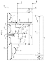
- a pre-driver circuit 10 may include two output terminals (pins) 10a, 10b which may be coupled to:
- One or more embodiments may rely on the use of a set of current mirrors (e.g. 11 to 19 in the figures). In one or more embodiments, these may be implemented according to principles known to those of skill in the art, thus making it unnecessary to provide a more detailed description herein.
- Ibias 10uA
- a charge pump CP e.g. high voltage up to 80V, assuming the battery voltage VB of Figures 1 to 3 may be e.g. + 15V.
- the bias current Ibias may be directed over three different paths through electronic switches (e.g. MOSFETs) SW1, SW2 and SW3.
- electronic switches e.g. MOSFETs
- just one switch may be ON (that is conductive) at a time according to the type (N-type or P-type) and connection arrangement (HS or LS) of the external switch S and as a function of the turn-on signals N-ON, P-ON, and the turn-off signal OFF applied as better detailed in the following.
- the switch SW1 may be coupled with a current mirror 15 which is supplied by the voltage source VS) and is in turn coupled with two further current mirrors 18 and 19 both referred to ground.
- the current mirrors 18 and 19 may be coupled (in a manner known per se) in such a way that the current mirror 19 may control (e.g. reduce) the bias current of the current mirror 18.
- the switch SW2 may be coupled to a current mirror 13 supplied by the charge pump CP, the current mirror 13 being connected (at 130) to the output terminal 10a (which may be coupled e.g. to the gate GN in Figures 1 and 3 or the source SP in Figure 2 ).
- the switch SW3 may be coupled to a current mirror 14 supplied by the charge pump CP, with the current mirror 14 communicating with a current mirror 17 connected (at 170) to the output terminal 10b (which may be coupled e.g. to the source SN in Figures 1 and 3 or the gate GP in Figure 2 ).
- a (pre)driver circuit 10 as exemplified herein may include two further current mirrors 12 and 16, a zener diode arrangement 190 plus an output diode 200 connected and operated as better detailed in the following.
- the switch SW1 may be turned ON (that is, made conductive) by applying thereto a command signal P-ON when an external PMOS providing the switch S is intended to be turned on by making it conductive.
- the output current of the current mirror 11 may provide a bias for the current mirror 15 (arrow A in Figure 5 ), which may in turn generate a new current towards the current mirror 18 (arrow B in Figure 5 ).
- the current mirror 18 will sink current (arrow C in Figure 5 ), possibly via the output diode 200, from the terminal 10b, which will decrease its voltage level.
- the voltage will continue to decrease until an internal clamp is activated.
- such internal clamp may include the zener diode arrangement 190 including e.g. two zener diodes arranged with their cathodes facing towards the output terminal 10a and coupled with the current mirror 16, set between the zener diode arrangement 190 and the output terminal 10b.
- the zener diode arrangement 190 including e.g. two zener diodes arranged with their cathodes facing towards the output terminal 10a and coupled with the current mirror 16, set between the zener diode arrangement 190 and the output terminal 10b.
- the current mirror 16 When the voltage difference (arrow D in Figure 5 ) between the two terminals 10a, 10b (here source SP and gate GP) reaches the clamp activation level (e.g. about 12V), the current mirror 16 will start generating a bias current to bias the current mirror 12 coupled to the charge pump CP (arrow E in Figure 5 ). This will in turn activate the current mirror 19 (arrow F in Figure 5 ) which may control the reduction of the bias current of the current mirror 18.
- the clamp activation level e.g. about 12V
- the arrangement as exemplified herein may be such that the higher the voltage difference between the two terminals or pins 10a, 10b, the higher the current flowing through the current mirror 19 will be: this will result in a corresponding reduction of the bias of the current mirror 18, so that the decrease of the voltage at the terminal 10b will be stopped at a desired level (e.g. about 12V between the source and the gate of the external PMOS).
- a desired level e.g. about 12V between the source and the gate of the external PMOS.
- the switch SW2 may be turned ON (that is, made conductive) by applying thereto a command signal N-ON when an external NMOS providing the switch S is intended to be turned on by making it conductive. This irrespective of whether a High Side (HS) or Low Side (LS) layout is being considered.
- HS High Side
- LS Low Side
- the output current from the current mirror 11 may be used to bias the current mirror 13 (arrow G in Figure 6 ), which may in turn generate a new current (arrow H in Figure 6 ) towards the node 130 coupled with the gate GN thus being able to increase the voltage level at the gate of the external NMOS.
- the internal clamp arrangement 190, 16 will thus operate as described previously for the PMOS case, when the voltage difference (again arrow D in Figure 6 ) between the two terminals 10a, 10b (here gate GN and source SN) reaches the clamp activation level (e.g. about 12V), with the current mirror 16 starting generating a bias current to bias the current mirror 12 (again arrow E in Figure 6 ).
- the clamp activation level e.g. about 12V
- the current mirror 12 will again produce a reduction in the bias current of the current mirror 13 that will stop its action when the voltage at 130 (here gate voltage GN) reaches a desired value as determined by the same internal clamp circuitry 190, 16 as used for the PMOS case discussed previously.
- the switch SW3 may be turned ON (that is, made conductive) by applying thereto a command signal OFF when an external component providing the switch S is intended to be turned off by making it non-conductive. This irrespective of whether NMOS or PMOS and irrespective of whether a High Side (HS) or Low Side (LS) layout is being considered.
- HS High Side
- LS Low Side
- the output current from the current mirror 11 may be used to bias the current mirror 14 (arrow L in Figure 7 ), with the current mirror 14 which generates a new current to the current mirror 17 (arrow M in Figure 7 ).
- MOS turn ON/OFF may be implemented with a controlled current on the gate of an external component, selectable e.g. via an SPI interface.
- AMR Absolute Maximum Rating, namely the maximum - positive or negative - voltage a pin can withstand while preserving device integrity
- AMR Absolute Maximum Rating, namely the maximum - positive or negative - voltage a pin can withstand while preserving device integrity
- pins 10a and 10b coupled to the gate and source of an external NMOS, -14V as negative AMR and +80V for 10a and +60V for 10b as positive AMR.
- the maximum differential voltage between 10a and 10b may be 20V (with circuit unpowered, namely with the voltage control loop between 10a and 10b inoperative).
- One or more embodiments may not merely rely on the juxtaposition of plural blocks that operate in parallel, and may take advantage of the possible re-use of circuitry for different purposes: just by way of non-limiting example, it will be appreciated that a same clamp circuit (e.g. the zener diode arrangement 190 having coupled therewith the current mirror 16) may be exploited for turning ON the external components, irrespective of the MOS type (N or P) and of the circuit layout (HS or LS) and for turning them OFF, thus saving silicon area.
- a same clamp circuit e.g. the zener diode arrangement 190 having coupled therewith the current mirror 16
- One or more embodiments may thus generate a voltage of e.g. 12V between the gate and source of an external MOS when this is intended to be driven ON, by activating an internal regulation loop which is different in the case of an external PMOS ( Figure 5 ) or an external NMOS ( Figure 6 ).
- such a loop may facilitate VGS regulation independently of the value of the charge pump CP (assuming that the charge pump voltage is high enough to permit correct operation of the circuit).
- a charge pump may de facto be dispensed with in the case of an external PMOS.
- One or more embodiments may thus provide a (pre)driver circuit 10 having a first and a second output terminal (e.g. 10a, 10b) for driving electronic switches (e.g. MOSFETs, either PMOS or NMOS) including a control terminal (e.g. a gate GN, GP, or possibly a base, in the case of a bipolar transistor or similar semiconductor switch) and a current path through the switch (e.g. source-drain in the case of a FET or possibly emitter-collector in the case of a bipolar transistor or similar semiconductor switch.
- a control terminal e.g. a gate GN, GP, or possibly a base, in the case of a bipolar transistor or similar semiconductor switch
- a current path through the switch e.g. source-drain in the case of a FET or possibly emitter-collector in the case of a bipolar transistor or similar semiconductor switch.
- coupling of the driver to the (external) electronic switch may include:
- the driver circuit may include:
- the voltage clamp (e.g. 190) may be coupled (e.g. via the current mirror 16, common to both the first and the second current mirror loops):
- the first current mirror loop may include:
- the first current mirror path may include a cascaded arrangement of:
- the first current mirror clamp arrangement may include a cascaded arrangement of:
- the second current mirror path may include a current mirror (e.g. 13) coupled to the second turn-on switch and the first output terminal to apply a voltage to the first output terminal.
- a current mirror e.g. 13
- the second current mirror clamp arrangement may include a cascaded arrangement of:
- the current mirror (e.g. 16) coupled to the voltage clamp is common to both said cascaded arrangements of said first current mirror clamp arrangement and said second current mirror clamp arrangement.
- the voltage clamp sensitive to the voltage across the first and second output terminals includes at least one zener diode (e.g. 190) having its anode and cathode facing towards the second output terminal and the first output terminal, respectively.
- at least one zener diode e.g. 190
- the third current mirror loop may include a turn-off current mirror path (e.g. current mirrors 14, 17) set between the turn-off switch and the first and second output terminals and configured to short circuit the first and second output terminals.
- a turn-off current mirror path e.g. current mirrors 14, 17
- One or more embodiments may provide a device (e.g. a driver for a lambda probe heater or other various kinds of electrical loads L) including:
- a method of driving (e.g. external) electronic switches including a control terminal and a current path through the switch by means of a driver circuit having a first and a second output terminal may include:
Landscapes
- Engineering & Computer Science (AREA)
- Physics & Mathematics (AREA)
- Microelectronics & Electronic Packaging (AREA)
- Nonlinear Science (AREA)
- Electromagnetism (AREA)
- General Physics & Mathematics (AREA)
- Radar, Positioning & Navigation (AREA)
- Automation & Control Theory (AREA)
- Electronic Switches (AREA)
Applications Claiming Priority (1)
| Application Number | Priority Date | Filing Date | Title |
|---|---|---|---|
| ITUB2016A000777A ITUB20160777A1 (it) | 2016-02-16 | 2016-02-16 | Circuito di pilotaggio, dispositivo e procedimento corrispondenti |
Publications (2)
| Publication Number | Publication Date |
|---|---|
| EP3208940A1 true EP3208940A1 (fr) | 2017-08-23 |
| EP3208940B1 EP3208940B1 (fr) | 2018-12-05 |
Family
ID=55861059
Family Applications (1)
| Application Number | Title | Priority Date | Filing Date |
|---|---|---|---|
| EP16191058.3A Active EP3208940B1 (fr) | 2016-02-16 | 2016-09-28 | Circuit d'attaque, dispositif et procédé correspondants |
Country Status (4)
| Country | Link |
|---|---|
| US (3) | US9929731B2 (fr) |
| EP (1) | EP3208940B1 (fr) |
| CN (2) | CN107086864B (fr) |
| IT (1) | ITUB20160777A1 (fr) |
Cited By (1)
| Publication number | Priority date | Publication date | Assignee | Title |
|---|---|---|---|---|
| IT201800001660A1 (it) * | 2018-01-23 | 2019-07-23 | St Microelectronics Grenoble 2 | Circuito di pilotaggio, sistema e procedimento corrispondenti |
Families Citing this family (3)
| Publication number | Priority date | Publication date | Assignee | Title |
|---|---|---|---|---|
| ITUB20160777A1 (it) * | 2016-02-16 | 2017-08-16 | St Microelectronics Srl | Circuito di pilotaggio, dispositivo e procedimento corrispondenti |
| JP7370210B2 (ja) * | 2019-10-04 | 2023-10-27 | ローム株式会社 | ゲートドライバ回路、モータドライバ回路、ハードディスク装置 |
| CN113541249B (zh) * | 2021-07-09 | 2023-08-01 | 旋智电子科技(上海)有限公司 | 基于预驱动模块实现充电路径控制的电路装置及电子设备 |
Citations (4)
| Publication number | Priority date | Publication date | Assignee | Title |
|---|---|---|---|---|
| US5757213A (en) * | 1996-08-16 | 1998-05-26 | Delco Electronics Corp. | Multi-configurable output driver |
| US20010030557A1 (en) * | 2000-04-12 | 2001-10-18 | Yukihide Niimi | Electrical load driving device |
| US6348820B1 (en) * | 2000-07-17 | 2002-02-19 | Motorola, Inc. | High-side, low-side configurable driver |
| DE10240167A1 (de) * | 2002-08-30 | 2004-03-18 | Infineon Technologies Ag | Schaltungsanordnung mit einem Leistungstransistor und einer Ansteuerschaltung für den Leistungstransistor |
Family Cites Families (9)
| Publication number | Priority date | Publication date | Assignee | Title |
|---|---|---|---|---|
| US7352786B2 (en) | 2001-03-05 | 2008-04-01 | Fuji Xerox Co., Ltd. | Apparatus for driving light emitting element and system for driving light emitting element |
| JP3847620B2 (ja) * | 2001-12-26 | 2006-11-22 | 日本テキサス・インスツルメンツ株式会社 | 駆動回路 |
| US6952120B2 (en) * | 2004-02-12 | 2005-10-04 | Texas Instruments Incorporated | Versatile system for controlling driver signal timing |
| US7579880B2 (en) * | 2006-03-23 | 2009-08-25 | Denso Corporation | Circuit for driving a semiconductor element |
| US7843246B2 (en) * | 2008-11-12 | 2010-11-30 | Texas Instruments Incorporated | Clamp control circuit having current feedback |
| US8885310B2 (en) * | 2012-10-31 | 2014-11-11 | Freescale Semiconductor, Inc. | Gate driver with desaturation detection and active clamping |
| CN103199696A (zh) * | 2013-04-24 | 2013-07-10 | 苏州硅智源微电子有限公司 | 用于场效应功率管栅极驱动的低功耗电荷泵 |
| US9106228B2 (en) * | 2013-06-23 | 2015-08-11 | Semiconductor Components Industries, Llc | Adaptive MOS transistor gate driver and method therefor |
| ITUB20160777A1 (it) * | 2016-02-16 | 2017-08-16 | St Microelectronics Srl | Circuito di pilotaggio, dispositivo e procedimento corrispondenti |
-
2016
- 2016-02-16 IT ITUB2016A000777A patent/ITUB20160777A1/it unknown
- 2016-09-24 US US15/275,363 patent/US9929731B2/en active Active
- 2016-09-28 EP EP16191058.3A patent/EP3208940B1/fr active Active
- 2016-12-30 CN CN201611259952.0A patent/CN107086864B/zh active Active
- 2016-12-30 CN CN201621487968.2U patent/CN206686154U/zh not_active Withdrawn - After Issue
-
2018
- 2018-02-19 US US15/898,931 patent/US10374603B2/en active Active
-
2019
- 2019-06-20 US US16/447,687 patent/US10879894B2/en active Active
Patent Citations (4)
| Publication number | Priority date | Publication date | Assignee | Title |
|---|---|---|---|---|
| US5757213A (en) * | 1996-08-16 | 1998-05-26 | Delco Electronics Corp. | Multi-configurable output driver |
| US20010030557A1 (en) * | 2000-04-12 | 2001-10-18 | Yukihide Niimi | Electrical load driving device |
| US6348820B1 (en) * | 2000-07-17 | 2002-02-19 | Motorola, Inc. | High-side, low-side configurable driver |
| DE10240167A1 (de) * | 2002-08-30 | 2004-03-18 | Infineon Technologies Ag | Schaltungsanordnung mit einem Leistungstransistor und einer Ansteuerschaltung für den Leistungstransistor |
Cited By (3)
| Publication number | Priority date | Publication date | Assignee | Title |
|---|---|---|---|---|
| IT201800001660A1 (it) * | 2018-01-23 | 2019-07-23 | St Microelectronics Grenoble 2 | Circuito di pilotaggio, sistema e procedimento corrispondenti |
| EP3514958A1 (fr) * | 2018-01-23 | 2019-07-24 | STMicroelectronics (Grenoble 2) SAS | Circuit d'attaque, système et procédé correspondants |
| US10784858B2 (en) | 2018-01-23 | 2020-09-22 | Stmicroelectronics S.R.L. | Driver circuit, corresponding system and method |
Also Published As
| Publication number | Publication date |
|---|---|
| CN107086864B (zh) | 2021-07-30 |
| US20170237427A1 (en) | 2017-08-17 |
| EP3208940B1 (fr) | 2018-12-05 |
| US20190305774A1 (en) | 2019-10-03 |
| US20180175856A1 (en) | 2018-06-21 |
| ITUB20160777A1 (it) | 2017-08-16 |
| US10879894B2 (en) | 2020-12-29 |
| CN206686154U (zh) | 2017-11-28 |
| US9929731B2 (en) | 2018-03-27 |
| US10374603B2 (en) | 2019-08-06 |
| CN107086864A (zh) | 2017-08-22 |
Similar Documents
| Publication | Publication Date | Title |
|---|---|---|
| US10879894B2 (en) | Driver circuit, corresponding device and method | |
| US8198818B2 (en) | Vehicle lighting control device | |
| US8203857B2 (en) | Booster device | |
| US8030986B2 (en) | Power transistor with turn off control and method for operating | |
| US10654428B2 (en) | Power supply control device | |
| US11251790B2 (en) | Power relay assembly for an electric vehicle and driving method thereof | |
| KR102351513B1 (ko) | 릴레이 작동을 위한 구동 회로 | |
| US20110317729A1 (en) | Current driving device | |
| US10268221B2 (en) | Power supply device and electronic control unit for lowering a minimum operating voltage and suppressing a consumed current to be low | |
| US20210281105A1 (en) | Circuit device | |
| CN108879627B (zh) | 电子模块和机动车辆及在接通过程中限制输入电流的方法 | |
| CN111211681A (zh) | 半导体装置 | |
| US7173350B2 (en) | Load drive control apparatus having minimized power consumption when functioning in waiting status | |
| US11411397B2 (en) | Polarity reversal protection circuit | |
| KR102434048B1 (ko) | 전자식 릴레이 장치 | |
| JP7302383B2 (ja) | 負荷駆動装置 | |
| JP7413860B2 (ja) | 給電制御装置 | |
| CN219611347U (zh) | 防反接电路、电源电路以及车辆 | |
| US11283442B2 (en) | Semiconductor device | |
| US20240128972A1 (en) | Switch device | |
| US20230133872A1 (en) | Gate control circuit, semiconductor device, electronic apparatus, and vehicle | |
| JP2023102546A (ja) | クランパ、入力回路、半導体装置 | |
| KR20240030322A (ko) | 저전압 동작이 가능한 led 구동 회로 | |
| JPH11141721A (ja) | 電磁弁駆動装置 |
Legal Events
| Date | Code | Title | Description |
|---|---|---|---|
| PUAI | Public reference made under article 153(3) epc to a published international application that has entered the european phase |
Free format text: ORIGINAL CODE: 0009012 |
|
| STAA | Information on the status of an ep patent application or granted ep patent |
Free format text: STATUS: THE APPLICATION HAS BEEN PUBLISHED |
|
| AK | Designated contracting states |
Kind code of ref document: A1 Designated state(s): AL AT BE BG CH CY CZ DE DK EE ES FI FR GB GR HR HU IE IS IT LI LT LU LV MC MK MT NL NO PL PT RO RS SE SI SK SM TR |
|
| AX | Request for extension of the european patent |
Extension state: BA ME |
|
| STAA | Information on the status of an ep patent application or granted ep patent |
Free format text: STATUS: REQUEST FOR EXAMINATION WAS MADE |
|
| 17P | Request for examination filed |
Effective date: 20171227 |
|
| RBV | Designated contracting states (corrected) |
Designated state(s): AL AT BE BG CH CY CZ DE DK EE ES FI FR GB GR HR HU IE IS IT LI LT LU LV MC MK MT NL NO PL PT RO RS SE SI SK SM TR |
|
| REG | Reference to a national code |
Ref country code: DE Ref legal event code: R079 Ref document number: 602016007784 Country of ref document: DE Free format text: PREVIOUS MAIN CLASS: H03K0017687000 Ipc: G05F0003260000 |
|
| GRAP | Despatch of communication of intention to grant a patent |
Free format text: ORIGINAL CODE: EPIDOSNIGR1 |
|
| STAA | Information on the status of an ep patent application or granted ep patent |
Free format text: STATUS: GRANT OF PATENT IS INTENDED |
|
| RIC1 | Information provided on ipc code assigned before grant |
Ipc: H03K 17/687 20060101ALI20180601BHEP Ipc: G05F 3/26 20060101AFI20180601BHEP Ipc: H03K 17/60 20060101ALI20180601BHEP |
|
| INTG | Intention to grant announced |
Effective date: 20180711 |
|
| GRAS | Grant fee paid |
Free format text: ORIGINAL CODE: EPIDOSNIGR3 |
|
| GRAA | (expected) grant |
Free format text: ORIGINAL CODE: 0009210 |
|
| STAA | Information on the status of an ep patent application or granted ep patent |
Free format text: STATUS: THE PATENT HAS BEEN GRANTED |
|
| AK | Designated contracting states |
Kind code of ref document: B1 Designated state(s): AL AT BE BG CH CY CZ DE DK EE ES FI FR GB GR HR HU IE IS IT LI LT LU LV MC MK MT NL NO PL PT RO RS SE SI SK SM TR |
|
| REG | Reference to a national code |
Ref country code: GB Ref legal event code: FG4D |
|
| REG | Reference to a national code |
Ref country code: CH Ref legal event code: EP |
|
| REG | Reference to a national code |
Ref country code: AT Ref legal event code: REF Ref document number: 1073849 Country of ref document: AT Kind code of ref document: T Effective date: 20181215 |
|
| REG | Reference to a national code |
Ref country code: IE Ref legal event code: FG4D |
|
| REG | Reference to a national code |
Ref country code: DE Ref legal event code: R096 Ref document number: 602016007784 Country of ref document: DE |
|
| REG | Reference to a national code |
Ref country code: NL Ref legal event code: MP Effective date: 20181205 |
|
| REG | Reference to a national code |
Ref country code: AT Ref legal event code: MK05 Ref document number: 1073849 Country of ref document: AT Kind code of ref document: T Effective date: 20181205 |
|
| REG | Reference to a national code |
Ref country code: LT Ref legal event code: MG4D |
|
| PG25 | Lapsed in a contracting state [announced via postgrant information from national office to epo] |
Ref country code: FI Free format text: LAPSE BECAUSE OF FAILURE TO SUBMIT A TRANSLATION OF THE DESCRIPTION OR TO PAY THE FEE WITHIN THE PRESCRIBED TIME-LIMIT Effective date: 20181205 Ref country code: ES Free format text: LAPSE BECAUSE OF FAILURE TO SUBMIT A TRANSLATION OF THE DESCRIPTION OR TO PAY THE FEE WITHIN THE PRESCRIBED TIME-LIMIT Effective date: 20181205 Ref country code: BG Free format text: LAPSE BECAUSE OF FAILURE TO SUBMIT A TRANSLATION OF THE DESCRIPTION OR TO PAY THE FEE WITHIN THE PRESCRIBED TIME-LIMIT Effective date: 20190305 Ref country code: HR Free format text: LAPSE BECAUSE OF FAILURE TO SUBMIT A TRANSLATION OF THE DESCRIPTION OR TO PAY THE FEE WITHIN THE PRESCRIBED TIME-LIMIT Effective date: 20181205 Ref country code: LV Free format text: LAPSE BECAUSE OF FAILURE TO SUBMIT A TRANSLATION OF THE DESCRIPTION OR TO PAY THE FEE WITHIN THE PRESCRIBED TIME-LIMIT Effective date: 20181205 Ref country code: NO Free format text: LAPSE BECAUSE OF FAILURE TO SUBMIT A TRANSLATION OF THE DESCRIPTION OR TO PAY THE FEE WITHIN THE PRESCRIBED TIME-LIMIT Effective date: 20190305 Ref country code: LT Free format text: LAPSE BECAUSE OF FAILURE TO SUBMIT A TRANSLATION OF THE DESCRIPTION OR TO PAY THE FEE WITHIN THE PRESCRIBED TIME-LIMIT Effective date: 20181205 Ref country code: AT Free format text: LAPSE BECAUSE OF FAILURE TO SUBMIT A TRANSLATION OF THE DESCRIPTION OR TO PAY THE FEE WITHIN THE PRESCRIBED TIME-LIMIT Effective date: 20181205 |
|
| PG25 | Lapsed in a contracting state [announced via postgrant information from national office to epo] |
Ref country code: AL Free format text: LAPSE BECAUSE OF FAILURE TO SUBMIT A TRANSLATION OF THE DESCRIPTION OR TO PAY THE FEE WITHIN THE PRESCRIBED TIME-LIMIT Effective date: 20181205 Ref country code: RS Free format text: LAPSE BECAUSE OF FAILURE TO SUBMIT A TRANSLATION OF THE DESCRIPTION OR TO PAY THE FEE WITHIN THE PRESCRIBED TIME-LIMIT Effective date: 20181205 Ref country code: GR Free format text: LAPSE BECAUSE OF FAILURE TO SUBMIT A TRANSLATION OF THE DESCRIPTION OR TO PAY THE FEE WITHIN THE PRESCRIBED TIME-LIMIT Effective date: 20190306 Ref country code: SE Free format text: LAPSE BECAUSE OF FAILURE TO SUBMIT A TRANSLATION OF THE DESCRIPTION OR TO PAY THE FEE WITHIN THE PRESCRIBED TIME-LIMIT Effective date: 20181205 |
|
| PG25 | Lapsed in a contracting state [announced via postgrant information from national office to epo] |
Ref country code: NL Free format text: LAPSE BECAUSE OF FAILURE TO SUBMIT A TRANSLATION OF THE DESCRIPTION OR TO PAY THE FEE WITHIN THE PRESCRIBED TIME-LIMIT Effective date: 20181205 |
|
| PG25 | Lapsed in a contracting state [announced via postgrant information from national office to epo] |
Ref country code: PT Free format text: LAPSE BECAUSE OF FAILURE TO SUBMIT A TRANSLATION OF THE DESCRIPTION OR TO PAY THE FEE WITHIN THE PRESCRIBED TIME-LIMIT Effective date: 20190405 Ref country code: CZ Free format text: LAPSE BECAUSE OF FAILURE TO SUBMIT A TRANSLATION OF THE DESCRIPTION OR TO PAY THE FEE WITHIN THE PRESCRIBED TIME-LIMIT Effective date: 20181205 Ref country code: IT Free format text: LAPSE BECAUSE OF FAILURE TO SUBMIT A TRANSLATION OF THE DESCRIPTION OR TO PAY THE FEE WITHIN THE PRESCRIBED TIME-LIMIT Effective date: 20181205 Ref country code: PL Free format text: LAPSE BECAUSE OF FAILURE TO SUBMIT A TRANSLATION OF THE DESCRIPTION OR TO PAY THE FEE WITHIN THE PRESCRIBED TIME-LIMIT Effective date: 20181205 |
|
| PG25 | Lapsed in a contracting state [announced via postgrant information from national office to epo] |
Ref country code: EE Free format text: LAPSE BECAUSE OF FAILURE TO SUBMIT A TRANSLATION OF THE DESCRIPTION OR TO PAY THE FEE WITHIN THE PRESCRIBED TIME-LIMIT Effective date: 20181205 Ref country code: SM Free format text: LAPSE BECAUSE OF FAILURE TO SUBMIT A TRANSLATION OF THE DESCRIPTION OR TO PAY THE FEE WITHIN THE PRESCRIBED TIME-LIMIT Effective date: 20181205 Ref country code: SK Free format text: LAPSE BECAUSE OF FAILURE TO SUBMIT A TRANSLATION OF THE DESCRIPTION OR TO PAY THE FEE WITHIN THE PRESCRIBED TIME-LIMIT Effective date: 20181205 Ref country code: RO Free format text: LAPSE BECAUSE OF FAILURE TO SUBMIT A TRANSLATION OF THE DESCRIPTION OR TO PAY THE FEE WITHIN THE PRESCRIBED TIME-LIMIT Effective date: 20181205 Ref country code: IS Free format text: LAPSE BECAUSE OF FAILURE TO SUBMIT A TRANSLATION OF THE DESCRIPTION OR TO PAY THE FEE WITHIN THE PRESCRIBED TIME-LIMIT Effective date: 20190405 |
|
| REG | Reference to a national code |
Ref country code: DE Ref legal event code: R097 Ref document number: 602016007784 Country of ref document: DE |
|
| PLBE | No opposition filed within time limit |
Free format text: ORIGINAL CODE: 0009261 |
|
| STAA | Information on the status of an ep patent application or granted ep patent |
Free format text: STATUS: NO OPPOSITION FILED WITHIN TIME LIMIT |
|
| PG25 | Lapsed in a contracting state [announced via postgrant information from national office to epo] |
Ref country code: SI Free format text: LAPSE BECAUSE OF FAILURE TO SUBMIT A TRANSLATION OF THE DESCRIPTION OR TO PAY THE FEE WITHIN THE PRESCRIBED TIME-LIMIT Effective date: 20181205 Ref country code: DK Free format text: LAPSE BECAUSE OF FAILURE TO SUBMIT A TRANSLATION OF THE DESCRIPTION OR TO PAY THE FEE WITHIN THE PRESCRIBED TIME-LIMIT Effective date: 20181205 |
|
| PGFP | Annual fee paid to national office [announced via postgrant information from national office to epo] |
Ref country code: FR Payment date: 20190821 Year of fee payment: 4 |
|
| 26N | No opposition filed |
Effective date: 20190906 |
|
| PG25 | Lapsed in a contracting state [announced via postgrant information from national office to epo] |
Ref country code: TR Free format text: LAPSE BECAUSE OF FAILURE TO SUBMIT A TRANSLATION OF THE DESCRIPTION OR TO PAY THE FEE WITHIN THE PRESCRIBED TIME-LIMIT Effective date: 20181205 |
|
| PG25 | Lapsed in a contracting state [announced via postgrant information from national office to epo] |
Ref country code: MC Free format text: LAPSE BECAUSE OF FAILURE TO SUBMIT A TRANSLATION OF THE DESCRIPTION OR TO PAY THE FEE WITHIN THE PRESCRIBED TIME-LIMIT Effective date: 20181205 |
|
| REG | Reference to a national code |
Ref country code: CH Ref legal event code: PL |
|
| PG25 | Lapsed in a contracting state [announced via postgrant information from national office to epo] |
Ref country code: IE Free format text: LAPSE BECAUSE OF NON-PAYMENT OF DUE FEES Effective date: 20190928 Ref country code: LU Free format text: LAPSE BECAUSE OF NON-PAYMENT OF DUE FEES Effective date: 20190928 Ref country code: CH Free format text: LAPSE BECAUSE OF NON-PAYMENT OF DUE FEES Effective date: 20190930 Ref country code: LI Free format text: LAPSE BECAUSE OF NON-PAYMENT OF DUE FEES Effective date: 20190930 |
|
| REG | Reference to a national code |
Ref country code: BE Ref legal event code: MM Effective date: 20190930 |
|
| PG25 | Lapsed in a contracting state [announced via postgrant information from national office to epo] |
Ref country code: BE Free format text: LAPSE BECAUSE OF NON-PAYMENT OF DUE FEES Effective date: 20190930 |
|
| GBPC | Gb: european patent ceased through non-payment of renewal fee |
Effective date: 20200928 |
|
| PG25 | Lapsed in a contracting state [announced via postgrant information from national office to epo] |
Ref country code: CY Free format text: LAPSE BECAUSE OF FAILURE TO SUBMIT A TRANSLATION OF THE DESCRIPTION OR TO PAY THE FEE WITHIN THE PRESCRIBED TIME-LIMIT Effective date: 20181205 |
|
| PG25 | Lapsed in a contracting state [announced via postgrant information from national office to epo] |
Ref country code: FR Free format text: LAPSE BECAUSE OF NON-PAYMENT OF DUE FEES Effective date: 20200930 Ref country code: HU Free format text: LAPSE BECAUSE OF FAILURE TO SUBMIT A TRANSLATION OF THE DESCRIPTION OR TO PAY THE FEE WITHIN THE PRESCRIBED TIME-LIMIT; INVALID AB INITIO Effective date: 20160928 Ref country code: MT Free format text: LAPSE BECAUSE OF FAILURE TO SUBMIT A TRANSLATION OF THE DESCRIPTION OR TO PAY THE FEE WITHIN THE PRESCRIBED TIME-LIMIT Effective date: 20181205 |
|
| PG25 | Lapsed in a contracting state [announced via postgrant information from national office to epo] |
Ref country code: GB Free format text: LAPSE BECAUSE OF NON-PAYMENT OF DUE FEES Effective date: 20200928 |
|
| PG25 | Lapsed in a contracting state [announced via postgrant information from national office to epo] |
Ref country code: MK Free format text: LAPSE BECAUSE OF FAILURE TO SUBMIT A TRANSLATION OF THE DESCRIPTION OR TO PAY THE FEE WITHIN THE PRESCRIBED TIME-LIMIT Effective date: 20181205 |
|
| PGFP | Annual fee paid to national office [announced via postgrant information from national office to epo] |
Ref country code: DE Payment date: 20230822 Year of fee payment: 8 |