EP3204992B1 - Elektrische steckverbinderanordnung - Google Patents
Elektrische steckverbinderanordnung Download PDFInfo
- Publication number
- EP3204992B1 EP3204992B1 EP15774930.0A EP15774930A EP3204992B1 EP 3204992 B1 EP3204992 B1 EP 3204992B1 EP 15774930 A EP15774930 A EP 15774930A EP 3204992 B1 EP3204992 B1 EP 3204992B1
- Authority
- EP
- European Patent Office
- Prior art keywords
- contact
- plug connector
- spring
- electrical
- configuration according
- Prior art date
- Legal status (The legal status is an assumption and is not a legal conclusion. Google has not performed a legal analysis and makes no representation as to the accuracy of the status listed.)
- Active
Links
Images


Classifications
-
- H—ELECTRICITY
- H01—ELECTRIC ELEMENTS
- H01R—ELECTRICALLY-CONDUCTIVE CONNECTIONS; STRUCTURAL ASSOCIATIONS OF A PLURALITY OF MUTUALLY-INSULATED ELECTRICAL CONNECTING ELEMENTS; COUPLING DEVICES; CURRENT COLLECTORS
- H01R13/00—Details of coupling devices of the kinds covered by groups H01R12/70 or H01R24/00 - H01R33/00
- H01R13/64—Means for preventing incorrect coupling
- H01R13/641—Means for preventing incorrect coupling by indicating incorrect coupling; by indicating correct or full engagement
-
- H—ELECTRICITY
- H01—ELECTRIC ELEMENTS
- H01R—ELECTRICALLY-CONDUCTIVE CONNECTIONS; STRUCTURAL ASSOCIATIONS OF A PLURALITY OF MUTUALLY-INSULATED ELECTRICAL CONNECTING ELEMENTS; COUPLING DEVICES; CURRENT COLLECTORS
- H01R13/00—Details of coupling devices of the kinds covered by groups H01R12/70 or H01R24/00 - H01R33/00
- H01R13/66—Structural association with built-in electrical component
- H01R13/70—Structural association with built-in electrical component with built-in switch
- H01R13/703—Structural association with built-in electrical component with built-in switch operated by engagement or disengagement of coupling parts, e.g. dual-continuity coupling part
- H01R13/7031—Shorting, shunting or bussing of different terminals interrupted or effected on engagement of coupling part, e.g. for ESD protection, line continuity
- H01R13/7032—Shorting, shunting or bussing of different terminals interrupted or effected on engagement of coupling part, e.g. for ESD protection, line continuity making use of a separate bridging element directly cooperating with the terminals
Definitions
- the present invention relates to an electrical connector assembly having mateable first and second connector parts, the first and second plug contact elements, and having an electrical connection detection means which produces an electrical connection between at least one contact spring and a contact strip in assembled connector parts, wherein the connection detection means on the first Connector part belongs to at least one contact spring with a molded spring contact, and wherein the connection detection device includes at least one contact strip on the second connector part, which is passed through a wall of the second connector part.
- Such a connector is from the German patent application DE 196 00 542 A1 known.
- a first connector part has a short-circuit contactor which electrically connects two connection detection connections to the second connector part after the connectors have been assembled.
- the connector parts of an electrical connector assembly have intended first and second plug-in contact elements, are transmitted via the after connection of the connector parts load currents or useful signals between the connected to the plug contact elements leads.
- some connector assemblies still have an electrical connection detector.
- An electrical connection detection device has the function of electrically and properly assembled connector parts To generate signal indicating the correct established plug-in connection.
- the signal can also be used to control the flow of current through the leads of the connector parts, so that, for example, the connector parts can be connected to each other without current.
- plug contact elements can be used as a connection detection device.
- the contacts of the connection detection device when connecting the connector parts close only when all other electrical connections are already made. Conversely, when disconnecting the connector parts, the contacts of the connection detection device are the first to be disconnected in order to signal the interruption of the connector as early as possible and possibly to enable a currentless disconnection of the plug contact elements.
- the second connector part has an electrically insulating projection which forms a rising in the joining direction of the connector parts guide bevel, that the at least one spring contact during assembly of the connector parts is guided over the guide slope and at the end of the joining process behind the projection the at least one contact strip is present.
- a ramp-like projection is thus provided, over which the at least one spring contact is guided during the assembly of the connector parts.
- the connector assembly can be carried out in a simple manner so that the electrical connection state of the connection detection contacts is sensitive to a precise positioning of the connector parts relative to each other. Incomplete connections are detected with high reliability.
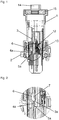
- the connector assembly consists of two interconnected connector parts 1, 2, which have mateable plug-sleeve-like first plug-in contact elements 12 and plug-type second plug-in contact elements 13, which can be designed in particular for high voltages and / or high load currents.
- a bushing 14 with a previously arranged radial seal 15 can be seen through which a connecting line, not shown, is guided in the interior of the first connector part 1, the conductor wires produce electrical connections to the first plug contact elements 12.
- the led out from the second connector part 2 end portions of the second plug contact elements 13 are also used to connect electrical leads.
- the specific embodiment of the electrical connections of the plug-in contact elements 12, 13 is of minor importance for the explanation of the invention and is therefore not shown in the drawing.
- the electrical connections can be carried out in a known manner, for example, as crimp, screw or plug connections.
- connection state can be used, for example, via the electrically controllable switching elements the Current flow on the plug contact elements 12, 13 of the connector assembly to release or interrupt.
- an electrical connection detection device which has a low Antechnischhysterese, so only when a fully prepared connector, that is, secured electrical connection, signaled an established connection and when disconnecting the connector no longer the presence of a complete connector by eliminating the connection signal as possible quickly recognizable.
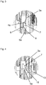
- FIGS. 1 to 4 A first embodiment of a connector assembly according to the invention is in the FIGS. 1 to 4 shown, wherein the FIGS. 2 to 4 in each case an enlargement of the in the FIG. 1 circular rimmed area shows.
- FIG. 2 discernible is a portion of a contact spring 3a, which forms a rounded spring contact 4a at its end portion.
- the rounded spring contact 4a rests with its convex-shaped side on a contact strip 5a, which belongs to the second connector part 2.
- the contact spring 3a is part of a contact spring element 3, which in perspective in the FIG. 9 is shown.
- the contact spring element 3 forms two mutually parallel contact springs 3a, 3b, which are integrally connected to each other via a connecting portion 16.
- a detent spring 17 is issued, which is provided for attachment of the contact spring element 3 on the first connector part 1.
- the contact spring element 3 made completely of metal takes over the function of a shorting bridge, which electrically connects two metal contact strips 5a, 5b arranged on the second connector part 2 as soon as the mechanical connection of the two connector parts 1, 2 is completely established.
- a shorting bridge which electrically connects two metal contact strips 5a, 5b arranged on the second connector part 2 as soon as the mechanical connection of the two connector parts 1, 2 is completely established.
- FIG. 2 shows the end position when connecting the connector parts 1, 2, in which the contact spring 3a bears against the contact strip 5a and thus produces an electrical connection to this. Since this applies equally to the contact spring 3b and the contact strip 5b, thus bridging the contact spring element 3 electrically the two contact strips 5a, 5b on the second connector part 2.
- the electrical connection of the contact strip 5a, 5b, by an unspecified electronics, the contact strips 5a, 5b is connected, easily detected and used for control or monitoring purposes.
- FIGS. 3 and 4 Two previous connection phases of the connector parts 1, 2 are represented by the representations of FIGS. 3 and 4 clarified.
- the rounded portion of the spring contacts 4a strikes a projection 6 made of an insulating material.
- the projection 6 forms a guide slope 7 in the form of an inclined plane rising in the plugging direction.
- the spring contact 4a slides up the projection 6, whereby the contact spring 3a is stretched perpendicular to the joining direction of the connector parts 1, 2.
- After exceeding a maximum point of the guide slope 7, shown in the FIG. 4 And driving over a short, slightly sloping area 18 of the locks Spring contact 4a finally behind the projection 6 and comes to the contact strip 5a to the plant, as in FIG. 2 was presented.
- relatively small abutment surfaces 8 for the spring contacts 4a, 4b can be specified on the contact strips 5a, 5b, so that the positions at which the spring contacts 4a, 4b can make electrical connections to the contact strips 5a, 5b are precisely defined.
- an insulating material surrounding the contact strips 5a, 5b leaves only contact surfaces 8 of small area as contact windows at which electrical connections to the spring contacts 4a, 4b can be made. This ensures that the connection detection device generates the connection signal only when the two connector parts 1, 2 are very precisely in their connection end position, in which the first and second plug contact elements 12, 13 are positioned correctly to each other.
- FIG. 2 shows further, the contact spring 3a above the spring contact 4a on an opposite curvature, whereby the contact spring engages closely to the region 18 of the projection 6.
- the sloping in the direction of connection of the connector parts 1, 2 region 18 forms in an opposite movement from a correspondingly increasing range, so that in a separation movement of the connector parts 1, 2 of the spring contact 4a is lifted after a short distance from the contact strip 5a.
- a separation of the connector parts 1, 2 is thus by the Connection detection device quickly detected, and in particular before electrical connections between the first and second plug-in contact elements 12, 13 are interrupted.
- FIGS. 5 to 8 Another and also advantageous embodiment of a connector assembly according to the invention is in the FIGS. 5 to 8 shown.
- This second embodiment differs from the first embodiment described above by the configuration of the electrical contact elements of its connection detection device.
- these contact elements do not form a shorting bridge on the first connector part 1, which bridge contact strips 5a, 5b on the second connector part 2, but an additional electrical connection between the first and the second connector part 1, 2 is made at correctly connected connector parts 1, 2.
- an electrical circuit arrangement which uses the signals of the connection detection device, and which functions this circuit arrangement concretely provides, either the embodiment of a connection detection device described above or below can be used particularly advantageously.
- connection detection contacts of the second embodiment are as individual parts in the FIG. 10 displayed.
- the contact arrangement according to FIG. 9 Be here for a connection detection non-parallel contact strips 5a, 5b connected to each other at the second connector part 2, but instead an electrical connection between a contact pin 10 on the first connector part 1 to a contact strip 5 on the second connector part 2 is made.
- the in the FIG. 10 shown contact arrangement can also be multiple in one Connector assembly are used to form about a multi-pole or redundant connection detection device.
- the electrical connection between the contact pin 10 and the contact strip 5 is mediated via a contact spring element 3 ', which has a U-shaped bent portion 9 which integrally connects two contact springs 3a', 3b 'together.
- the contact springs 3a ', 3b' form at their outer end portions in each case a spring contact 4a ', 4b' from.
- the spring contact 4b ' is located on the in the first connector part 1' arranged contact pin 10, whereby it is electrically connected to the contact spring element 3 '.
- the spring contact 4b' is not moved against the contact pin 10 and thus forms with this a fixed electrical connection.
- a connection lead leading out of the first connector part 1 ' can be fastened to the crimping portion 11 of the contact pin 10.
- the contact pin 10 could also be made in one piece with the contact spring element 3 '. But this would lead to a relatively complex shaped object that would be expensive to manufacture and assemble. It would also be necessary to dispense with the possibility of choosing different materials for the contact spring element 3 'and the contact pin 10. For these reasons, it is advantageous to electrically connect the contact pin 10, as shown here, via the spring contact 4b '.
- the spring contact 4a ' is, completely analogous to the first embodiment also here when connecting the two connector parts 1', 2 guided over a projection 6 and is behind the projection 6 on the contact strip 5, whereby the electrical contacts of the connection detection means are closed.
- the constructions and Processes in the FIGS. 6 to 8 Compound phases shown completely correspond to those already using the FIGS. 2 to 4 described procedures, so that can be dispensed with a further explanation at this point.
Landscapes
- Details Of Connecting Devices For Male And Female Coupling (AREA)
- Connector Housings Or Holding Contact Members (AREA)
Description
- Die vorliegende Erfindung betrifft eine elektrische Steckverbinderanordnung mit zusammenfügbaren ersten und zweiten Steckverbinderteilen, die erste und zweite Steckkontaktelemente aufweisen, und die eine elektrische Verbindungsnachweiseinrichtung aufweist, die bei zusammengefügten Steckverbinderteilen eine elektrische Verbindung zwischen mindestens einer Kontaktfeder und einem Kontaktstreifen herstellt, wobei zu der Verbindungsnachweiseinrichtung am ersten Steckverbinderteil mindestens eine Kontaktfeder mit einem angeformten Federkontakt gehört, und wobei zu der Verbindungsnachweiseinrichtung mindestens ein Kontaktstreifen am zweiten Steckverbinderteil gehört, der durch eine Wand des zweiten Steckverbinderteils hindurchgeführt ist.
- Ein derartiger Steckverbinder ist aus der deutschen Offenlegungsschrift
DE 196 00 542 A1 bekannt. Hierbei weist ein erstes Steckverbinderteil einen Kurzschluss-Kontaktgeber auf, der nach dem Zusammenfügen der Steckverbinder zwei Verbindungsnachweisanschlüsse an dem zweiten Steckverbinderteil elektrisch miteinander verbindet. - Die Steckverbinderteile einer elektrischen Steckverbinderanordnung weisen bestimmungsgemäß erste und zweite Steckkontaktelemente auf, über die nach dem Zusammenfügen der Steckverbinderteile Lastströme oder Nutzsignale zwischen den mit den Steckkontaktelementen verbundenen Zuleitungen übertragen werden. Darüber hinaus weisen manche Steckverbinderanordnungen noch eine elektrische Verbindungsnachweiseinrichtung auf.
- Eine elektrische Verbindungsnachweiseinrichtung hat die Funktion, bei korrekt und vollständig zusammengefügten Steckverbinderteilen ein elektrisches Signal zu erzeugen, welches die korrekte hergestellte Steckverbindung anzeigt. Das Signal kann auch dazu verwendet werden, den Stromfluss durch die Zuleitungen der Steckverbinderteile zu steuern, so dass beispielsweise die Steckverbinderteile stromlos miteinander verbunden werden können.
- Bei vielpoligen Steckverbinderanordnungen können nicht anderweitig benötigte Steckkontaktelemente als Verbindungsnachweiseinrichtung verwendet werden. Dieses führt allerdings zu nachteiligen Eigenschaften, und zwar insbesondere dadurch, dass axial zusammengeführte Steckverbinder immer einen gewissen Steckweg aufweisen, und so die Kontakte der Verbindungsnachweiseinrichtung einander berühren und ein Signal generieren können, bevor der Steckvorgang vollständig abgeschlossen und eine sichere Verbindung aller Steckkontaktelemente gewährleistet ist.
- Aus Sicherheitsgründen und zur Vermeidung von Schaltfunken ist es wünschenswert, dass die Kontakte der Verbindungsnachweiseinrichtung beim Verbinden der Steckverbinderteile erst dann schließen, wenn alle anderen elektrischen Verbindungen bereits hergestellt sind. Umgekehrt sollen beim Trennen der Steckverbinderteile die Kontakte der Verbindungsnachweiseinrichtung als erstes getrennt werden, um die Unterbrechung der Steckverbindung möglichst frühzeitig zu signalisieren und gegebenenfalls ein stromloses Trennen der Steckkontaktelemente zu ermöglichen.
- Es stellte sich daher die Aufgabe, einen elektrischen Steckverbinder mit zusammenfügbaren Steckverbinderteilen und mit einer elektrischen Verbindungsnachweiseinrichtung zu schaffen, welche die vorgenannten Anforderungen auf einfache und kostengünstige Weise sicher erfüllt.
- Diese Aufgabe wird erfindungsgemäß dadurch gelöst, dass das zweite Steckverbinderteil einen elektrisch isolierenden Vorsprung aufweist, der eine in Fügerichtung der Steckverbinderteile ansteigende Führungsschräge ausbildet, dass der mindestens eine Federkontakt beim Zusammenfügen der Steckverbinderteile über die Führungsschräge geführt wird und am Ende des Fügevorgangs hinter dem Vorsprung an dem mindestens einen Kontaktstreifen anliegt.
- Erfindungsgemäß ist somit ein rampenartiger Vorsprung vorgesehen, über den der mindestens eine Federkontakt beim Zusammenfügen der Steckverbinderteile geführt wird. Wie nachfolgend dargelegt wird, kann hierdurch ein sehr schnelles und positionsgenaues Verbinden und auch Trennen der Verbindungsnachweiskontakte erreicht werden. Die Steckverbinderanordnung kann dabei auf einfache Weise so ausgeführt werden, dass der elektrische Verbindungszustand der Verbindungsnachweiskontakte empfindlich von einer genauen Positionierung der Steckverbinderteile relativ zueinander abhängt. Unvollständig hergestellte Steckverbindungen werden dadurch mit hoher Zuverlässigkeit erkannt.
- Im Folgenden sollen zwei vorteilhafte Ausführungsbeispiele der Erfindung anhand der Zeichnung dargestellt und näher erläutert werden. Es zeigen
- Figur 1 Figuren 2 bis 4
- die Schnittansicht einer ersten Steckverbinderanordnung, drei Phasen des Verbindens der Steckverbinderteile der ersten Steckverbinderanordnung, dargestellt anhand von Ausschnittsvergrößerungen,
- Figur 5 Figuren 6 bis 8
- die Schnittansicht einer zweiten Steckverbinderanordnung, drei Phasen des Verbindens der Steckverbinderteile der zweiten Steckverbinderanordnung, dargestellt anhand von Ausschnittsvergrößerungen,
- Figur 9
- die Verbindungsnachweiskontakte der ersten Steckverbinderanordnung,
- Figur 10
- die Verbindungsnachweiskontakte der zweiten Steckverbinderanordnung.
- In der
Figur 1 ist eine elektrische Steckverbinderanordnung dargestellt, wie sie insbesondere in Kraftfahrzeugen vorteilhaft verwendet werden kann. Die Steckverbinderanordnung besteht aus zwei miteinander verbundenen Steckverbinderteilen 1, 2, welche zusammenfügbare steckhülsenartige erste Steckkontaktelemente 12 und steckerartige zweite Steckkontaktelemente 13 aufweisen, die insbesondere für hohe Spannungen und/oder hohe Lastströme ausgelegt sein können. - Am ersten Steckverbinderteil 1 ist eine Durchführung 14 mit einer davor angeordneten Radialdichtung 15 erkennbar, durch die hindurch eine nicht dargestellte Anschlussleitung in das Innere des ersten Steckverbinderteils 1 geführt wird, deren Leitungsadern elektrische Verbindungen zu den ersten Steckkontaktelementen 12 herstellen. Die aus dem zweiten Steckverbinderteil 2 herausgeführten Endabschnitte der zweiten Steckkontaktelemente 13 dienen ebenfalls zum Anschluss elektrischer Zuleitungen. Die konkrete Ausgestaltung der elektrische Anbindungen der Steckkontaktelemente 12, 13 ist für die Erläuterung der Erfindung von untergeordneter Bedeutung und ist daher in der Zeichnung nicht darstellt. Die elektrischen Anbindungen können auf bekannte Weise beispielsweise als Crimp-, Schraub- oder Steckverbindungen ausgeführt sein.
- Für viele Anwendungen ist es wichtig, den mechanischen und elektrischen Verbindungszustand der Steckverbinderanordnung genau ermitteln zu können. Die Information über den Verbindungszustand kann beispielsweise verwendet werden, um über elektrisch steuerbare Schaltelemente den Stromfluss über die Steckkontaktelemente 12, 13 der Steckverbinderanordnung freizugeben oder zu unterbrechen.
- Vorteilhaft ist hierzu eine elektrische Verbindungsnachweiseinrichtung, die eine geringe Ansprechhysterese aufweist, die also erst bei einer vollständig hergestellten Steckverbindung, das heißt, sichergestellter elektrischer Verbindung, eine hergestellte Verbindung signalisiert und beim Trennen der Steckverbindung das nicht mehr Vorliegen einer vollständigen Steckverbindung durch Wegfall des Verbindungssignals möglichst schnell erkennbar macht.
- Eine erste Ausführung einer erfindungsgemäßen Steckverbinderanordnung ist in den
Figuren 1 bis 4 dargestellt, wobei dieFiguren 2 bis 4 jeweils eine Vergrößerung des in derFigur 1 kreisförmig umrandeten Bereichs zeigt. In derFigur 2 erkennbar ist ein Abschnitt einer Kontaktfeder 3a, die an ihrem Endabschnitt einen abgerundeten Federkontakt 4a ausbildet. Der abgerundete Federkontakt 4a liegt mit seiner konvex geformten Seite an einem Kontaktstreifen 5a an, welcher zum zweiten Steckverbinderteil 2 gehört. - Die Kontaktfeder 3a ist Teil eines Kontaktfederelements 3, welches perspektivisch in der
Figur 9 dargestellt ist. Das Kontaktfederelement 3 bildet zwei parallel zueinander angeordnete Kontaktfedern 3a, 3b aus, die über einen Verbindungsabschnitt 16 einstückig miteinander verbunden sind. Am Verbindungsabschnitt 16 ist eine Rastfeder 17 ausgestellt, welche zur Befestigung des Kontaktfederelements 3 am ersten Steckverbinderteil 1 vorgesehen ist. - Als Teil der erfindungsgemäß ausgeführten Verbindungsnachweiseinrichtung übernimmt das vollständig aus Metall bestehende Kontaktfederelement 3 die Funktion einer Kurzschlussbrücke, welche zwei am zweiten Steckverbinderteil 2 angeordnete metallene Kontaktstreifen 5a, 5b elektrisch miteinander verbindet, sobald die mechanische Verbindung der beiden Steckverbinderteile 1, 2 vollständig hergestellt ist. In den Schnittansichten der
Figuren 1 bis 4 ist jeweils nur eine Kontaktfeder 3a und ein Kontaktstreifen 5a erkennbar; deren Funktionsbeschreibung trifft aber analog auch auf die dort nicht dargestellte Kontaktfeder 3b und den zugehörigen Kontaktstreifen 5b zu. - Die
Figur 2 zeigt die Endposition beim Verbinden der Steckverbinderteile 1, 2, in der die Kontaktfeder 3a am Kontaktstreifen 5a anliegt und so zu diesem eine elektrische Verbindung herstellt. Da dies gleichermaßen für Kontaktfeder 3b und den Kontaktstreifen 5b gilt, überbrückt somit das Kontaktfederelement 3 elektrisch die beiden Kontaktstreifen 5a, 5b am zweiten Steckverbinderteil 2. Die elektrische Verbindung der Kontaktstreifen 5a, 5b kann durch eine hier nicht näher beschriebene Elektronik, die an die Kontaktstreifen 5a, 5b angeschlossen ist, leicht erfasst und für Steuerungs- oder Überwachungszwecke verwendet werden. - Zwei vorhergehende Verbindungsphasen der Steckverbinderteile 1, 2 werden durch die Darstellungen der
Figuren 3 und 4 verdeutlicht. In der ersten Phase des Zusammenfügens (Figur 3 ) der beiden Steckverbinderteile 1, 2 trifft der abgerundete Abschnitt der Federkontakte 4a auf einen aus einem Isoliermaterial bestehenden Vorsprung 6. Der Vorsprung 6 bildet eine Führungsschräge 7 in Form einer in der Steckrichtung ansteigenden schiefen Ebene aus. Entlang dieser Führungsschräge 7 gleitet der Federkontakt 4a den Vorsprung 6 hinauf, wodurch die Kontaktfeder 3a senkrecht zur Fügerichtung der Steckverbinderteile 1, 2 gespannt wird. Nach Überschreiten eines höchstens Punkts der Führungsschräge 7, dargestellt in derFigur 4 , und Überfahren eines kurzen, leicht abfallenden Bereiches 18 rastet der Federkontakt 4a schließlich hinter dem Vorsprung 6 ein und kommt am Kontaktstreifen 5a zur Anlage, wie inFigur 2 dargestellt wurde. - Besonders vorteilhaft an der erfindungsgemäßen Ausführung ist, dass die mechanische und elektrische Verbindung zwischen den Federkontakten 4a, 4b und den Kontaktstreifen 5a, 5b durch den vorgelagerten Vorsprung 6 sehr schnell und durch die mechanisch vorgespannten Kontaktfedern 3a, 3b quasi sprunghaft erfolgt.
- Vorteilhafterweise können an den Kontaktstreifen 5a, 5b relativ kleine Anlageflächen 8 für die Federkontakte 4a, 4b vorgegeben werden, so dass die Positionen, an denen die Federkontakte 4a, 4b elektrische Verbindungen zu den Kontaktstreifen 5a, 5b herstellen können genau definiert sind. Hierzu kann vorzugsweise vorgesehen sein, dass ein die Kontaktstreifen 5a, 5b umgebendes Isoliermaterial lediglich kleinflächige Anlageflächen 8 als Kontaktfenster freilässt, an denen elektrische Verbindungen zu den Federkontakten 4a, 4b hergestellt werden können. Dadurch ist sichergestellt, dass die Verbindungsnachweiseinrichtung das Verbindungssignal nur dann generiert, wenn sich die beiden Steckverbinderteile 1, 2 sehr präzise in ihrer Verbindungsendposition befinden, in der auch die ersten und zweiten Steckkontaktelemente 12, 13 korrekt zueinander positioniert sind.
- Wie die
Figur 2 weiter zeigt, weist die Kontaktfeder 3a oberhalb des Federkontakts 4a eine gegenläufige Krümmung auf, wodurch die Kontaktfeder eng an dem Bereich 18 des Vorsprungs 6 anliegt. Der in Verbindungsrichtung der Steckverbinderteile 1, 2 abfallenden Bereich 18 bildet bei einer gegenläufigen Bewegung einen entsprechend ansteigenden Bereich aus, so dass bei einer Trennbewegung der Steckverbinderteile 1, 2 der Federkontakt 4a schon nach einem kurzen Weg von dem Kontaktstreifen 5a abgehoben wird. Eine Trennung der Steckverbinderteile 1, 2 wird somit durch die Verbindungsnachweiseinrichtung schnell erkannt, und zwar insbesondere bevor elektrische Verbindungen zwischen ersten und zweiten Steckkontaktelementen 12, 13 unterbrochen werden. - Eine weitere und ebenfalls vorteilhafte Ausführung einer erfindungsgemäßen Steckverbinderanordnung ist in den
Figuren 5 bis 8 dargestellt. Diese zweite Ausführung unterscheidet sich von der zuvor beschriebenen ersten Ausführung durch die Ausgestaltung der elektrischen Kontaktelemente seiner Verbindungsnachweisvorrichtung. - Speziell bilden diese Kontaktelemente hier keine Kurzschlussbrücke am ersten Steckverbinderteil 1 aus, welche Kontaktstreifen 5a, 5b am zweiten Steckverbinderteil 2 überbrücken, sondern es wird bei korrekt verbundenen Steckverbinderteilen 1, 2 eine zusätzliche elektrische Verbindung zwischen dem ersten und dem zweiten Steckverbinderteil 1, 2 hergestellt. Abhängig davon, wo eine elektrische Schaltungsanordnung angeordnet ist, welche die Signale der Verbindungsnachweisvorrichtung verwendet, und welche Funktionen diese Schaltungsanordnung konkret vorsieht, kann entweder die zuvor oder die nachfolgend beschriebene Ausführung einer Verbindungsnachweisvorrichtung besonders vorteilhaft einsetzbar sein.
- Die Verbindungsnachweiskontakte des zweiten Ausführungsbeispiels sind als Einzelteile in der
Figur 10 abgebildet. Im Unterschied zu der Kontaktanordnung nachFigur 9 werden hier für einen Verbindungsnachweis nicht parallele Kontaktstreifen 5a, 5b am zweiten Steckverbinderteil 2 miteinander verbunden, sondern es wird statt dessen eine elektrische Verbindung zwischen einem Kontaktstift 10 am ersten Steckverbinderteil 1 zu einem Kontaktstreifen 5 am zweiten Steckverbinderteil 2 hergestellt. Die in derFigur 10 dargestellte Kontaktanordnung kann auch mehrfach in einer Steckverbinderanordnung zur Anwendung kommen, um etwa eine mehrpolige oder redundant wirkende Verbindungsnachweisvorrichtung auszubilden. - Die elektrische Verbindung zwischen dem Kontaktstift 10 und dem Kontaktstreifen 5 wird über ein Kontaktfederelement 3' vermittelt, welches einen u-förmig gebogenen Abschnitt 9 aufweist, der einstückig zwei Kontaktfedern 3a', 3b' miteinander verbindet. Die Kontaktfedern 3a', 3b' bilden an ihren äußeren Endabschnitten jeweils einen Federkontakt 4a', 4b' aus.
- Wie die
Figur 5 zeigt, liegt der Federkontakt 4b' an dem im ersten Steckverbinderteil 1' angeordneten Kontaktstift 10 an, wodurch dieser mit dem Kontaktfederelement 3' elektrisch verbunden ist. Im Gegensatz zu dem Federkontakt 4a' und dem Kontaktstreifen 5 wird der Federkontakt 4b' nicht gegen den Kontaktstift 10 bewegt und bildet somit mit diesem eine feststehende elektrische Verbindung aus. Eine aus dem ersten Steckverbinderteil 1' herausführende Anschlussleitung kann an dem Crimpabschnitt 11 des Kontaktstifts 10 befestigt werden. - Grundsätzlich könnte der Kontaktstift 10 auch einstückig mit dem Kontaktfederelement 3' ausgeführt werden. Dieses würde aber zu einem relativ komplex geformten Gegenstand führen, der aufwendig herzustellen und zu montieren wäre. Auch müsste man auf die Möglichkeit, unterschiedliche Materialien für das Kontaktfederelement 3' und den Kontaktstift 10 zu wählen, verzichten. Aus diesen Gründen ist es vorteilhaft, den Kontaktstift 10, wie hier dargestellt, über den Federkontakt 4b' elektrisch anzubinden.
Der Federkontakt 4a' wird, vollkommen analog zum ersten Ausführungsbeispiel auch hier beim Verbinden der beiden Steckverbinderteile 1', 2 über einen Vorsprung 6 geführt und liegt hinter dem Vorsprung 6 an dem Kontaktstreifen 5 an, wodurch die elektrische Kontakte der Verbindungsnachweiseinrichtung geschlossen sind. Die Aufbauten und Abläufe der in denFiguren 6 bis 8 dargestellten Verbindungsphasen entsprechen vollständig den bereits anhand derFiguren 2 bis 4 beschriebenen Abläufen, so dass auf eine weitere Erläuterung an dieser Stelle verzichtet werden kann. -
- 1, 1'
- (erstes) Steckverbinderteil
- 2
- (zweites) Steckverbinderteil
- 3, 3'
- Kontaktfederelement
- 3a, 3b, 3a', 3b'
- Kontaktfedern
- 4a, 4b, 4a', 4b'
- Federkontakte
- 5, 5a, 5b
- Kontaktstreifen
- 6
- Vorsprung
- 7
- Führungsschräge
- 8
- Anlageflächen
- 9
- u-förmig gebogener Abschnitt
- 10
- Kontaktstifte
- 11
- Crimpabschnitt
- 12
- erste Steckkontaktelemente
- 13
- zweite Steckkontaktelemente
- 14
- Durchführung
- 15
- Radialdichtung
- 16
- Verbindungsabschnitt
- 17
- Rastfeder
- 18
- abfallender Bereich
Claims (8)
- Elektrische Steckverbinderanordnung mit zusammenfügbaren ersten und zweiten Steckverbinderteilen (1, 2; 1', 2), die erste und zweite Steckkontaktelemente (12, 13) aufweisen,
und die eine elektrische Verbindungsnachweiseinrichtung aufweist, die bei zusammengefügten Steckverbinderteilen (1, 2; 1', 2) eine elektrische Verbindung zwischen mindestens einem Federkontakt (4a, 4b, 4a') und einem Kontaktstreifen (5a, 5b, 5) herstellt,
wobei zu der Verbindungsnachweiseinrichtung am ersten Steckverbinderteil (1) mindestens eine Kontaktfeder (3a, 3b; 3a') mit einem angeformten Federkontakt (4a, 4b; 4a') gehört, und
wobei zu der Verbindungsnachweiseinrichtung mindestens ein Kontaktstreifen (5a, 5b) am zweiten Steckverbinderteil (2) gehört, der durch eine Wand des zweiten Steckverbinderteils (2) hindurchgeführt ist,
dadurch gekennzeichnet,
dass das zweite Steckverbinderteil (2) einen elektrisch isolierenden Vorsprung (6) aufweist, der eine in Fügerichtung der Steckverbinderteile (1, 2) ansteigende Führungsschräge (7) ausbildet,
dass der mindestens eine Federkontakt (4a, 4b; 4a') beim Zusammenfügen der Steckverbinderteile (1, 2; 1', 2) über die Führungsschräge (7) geführt wird und am Ende des Fügevorgangs hinter dem Vorsprung (6) an dem mindestens einen Kontaktstreifen (5a, 5b; 5) anliegt. - Elektrische Steckverbinderanordnung nach Anspruch 1, dadurch gekennzeichnet, dass ein metallenes Kontaktfederelement (3; 3') einstückig zwei Kontaktfedern (3a, 3b; 3a', 3b') aufweist.
- Elektrische Steckverbinderanordnung nach Anspruch 2, dadurch gekennzeichnet, dass zwei Kontaktfeder (3a, 3b) parallel nebeneinander angeordnet sind und einstückig über einen Verbindungsabschnitt (16) miteinander verbunden sind.
- Elektrische Steckverbinderanordnung nach Anspruch 3, dadurch gekennzeichnet, dass der Verbindungsabschnitt (16) eine Rastfeder (17) aufweist.
- Elektrische Steckverbinderanordnung nach Anspruch 3, dadurch gekennzeichnet, dass die beiden Kontaktfedern (3a, 3b) Federkontakte (4a, 4b) aufweisen, die an jeweils einen Kontaktstreifen (5a, 5b) am zweiten Steckverbinderteil (2) anfügbar sind und im angefügten Zustand die Kontaktstreifen (5a, 5b) elektrisch miteinander verbinden.
- Elektrische Steckverbinderanordnung nach Anspruch 2, dadurch gekennzeichnet, dass die beiden Kontaktfedern (3a', 3b') über einen u-förmig gebogenen Abschnitt (9) miteinander verbunden sind, und der Federkontakt (4a') der einen Kontaktfeder (3a') an einen Kontaktstreifen (5) am zweiten Steckverbinderteil (2) anfügbar ist und der Federkontakt (4b') der anderen Kontaktfeder (3b') an einem zum ersten Steckverbinderteil (1) gehörenden Kontaktstift (10) anliegt.
- Elektrische Steckverbinderanordnung nach Anspruch 1, dadurch gekennzeichnet, dass der Vorsprung (6) in Fügerichtung der Steckverbinderteile (1, 2) auf die ansteigende Führungsschräge (7) folgend einen abfallenden Bereich (18) aufweist, wobei der abfallende Bereich (18) kürzer ist als die Führungsschräge (7).
- Elektrische Steckverbinderanordnung nach Anspruch 1, dadurch gekennzeichnet, dass die Federkontakte (4a, 4b, 4a', 4b') einen abgerundeten und vorzugsweise halbkreisförmigen Querschnitt aufweisen.
Applications Claiming Priority (2)
| Application Number | Priority Date | Filing Date | Title |
|---|---|---|---|
| DE102014015027.5A DE102014015027A1 (de) | 2014-10-09 | 2014-10-09 | Elektrische Steckverbinderanordnung |
| PCT/EP2015/073044 WO2016055474A1 (de) | 2014-10-09 | 2015-10-06 | Elektrische steckverbinderanordnung |
Publications (2)
| Publication Number | Publication Date |
|---|---|
| EP3204992A1 EP3204992A1 (de) | 2017-08-16 |
| EP3204992B1 true EP3204992B1 (de) | 2018-06-27 |
Family
ID=54251522
Family Applications (1)
| Application Number | Title | Priority Date | Filing Date |
|---|---|---|---|
| EP15774930.0A Active EP3204992B1 (de) | 2014-10-09 | 2015-10-06 | Elektrische steckverbinderanordnung |
Country Status (10)
| Country | Link |
|---|---|
| US (1) | US9787026B2 (de) |
| EP (1) | EP3204992B1 (de) |
| JP (1) | JP6635522B2 (de) |
| KR (1) | KR102349635B1 (de) |
| CN (1) | CN107078444B (de) |
| BR (1) | BR112017004509B1 (de) |
| DE (1) | DE102014015027A1 (de) |
| ES (1) | ES2688045T3 (de) |
| MX (1) | MX2017004500A (de) |
| WO (1) | WO2016055474A1 (de) |
Family Cites Families (15)
| Publication number | Priority date | Publication date | Assignee | Title |
|---|---|---|---|---|
| US4298237A (en) * | 1979-12-20 | 1981-11-03 | Bell Telephone Laboratories, Incorporated | Printed wiring board interconnection apparatus |
| US4900267A (en) * | 1988-05-30 | 1990-02-13 | Yazaki Corporation | Harness connector having an engagement check structure |
| JPH082941Y2 (ja) * | 1988-05-30 | 1996-01-29 | 矢崎総業株式会社 | 不完全ロック検出機能を有するハーネスコネクタおよび不完全ロックの自動検出装置 |
| JP2853834B2 (ja) * | 1990-06-20 | 1999-02-03 | 住友電装 株式会社 | コネクタの接続検出装置 |
| US5088931A (en) * | 1990-12-24 | 1992-02-18 | At&T Bell Laboratories | Apparatus for sequencing signals in conjunction with shorting contacts |
| JP3264305B2 (ja) * | 1995-01-09 | 2002-03-11 | 矢崎総業株式会社 | 結合検知装置を備えたコネクタ |
| JPH0917510A (ja) * | 1995-06-29 | 1997-01-17 | Sumitomo Wiring Syst Ltd | 嵌合検知コネクタ |
| JP3415008B2 (ja) | 1997-11-12 | 2003-06-09 | 住友電装株式会社 | コネクタ |
| JP2004327321A (ja) * | 2003-04-25 | 2004-11-18 | Jst Mfg Co Ltd | コネクタ |
| JP4606283B2 (ja) * | 2005-09-12 | 2011-01-05 | 矢崎総業株式会社 | コネクタ |
| EP1775801B1 (de) * | 2005-09-29 | 2009-09-23 | Sumitomo Wiring Systems, Ltd. | Ein Steckverbinder mit einem bewegbaren Glied |
| JP4492509B2 (ja) * | 2005-09-29 | 2010-06-30 | 住友電装株式会社 | レバー式コネクタ |
| WO2007072494A1 (en) * | 2005-12-23 | 2007-06-28 | Naik Praful Ramchandra | Metallized packaging blister container |
| JP5863198B2 (ja) * | 2010-08-19 | 2016-02-16 | エフシーアイ・オートモティヴ・ホールディング | 車両内において車両用電力を供給又は伝送するためのコネクタ装置及びコネクタ組立体 |
| JP6085515B2 (ja) * | 2013-04-26 | 2017-02-22 | 矢崎総業株式会社 | コネクタ |
-
2014
- 2014-10-09 DE DE102014015027.5A patent/DE102014015027A1/de not_active Withdrawn
-
2015
- 2015-10-06 EP EP15774930.0A patent/EP3204992B1/de active Active
- 2015-10-06 ES ES15774930.0T patent/ES2688045T3/es active Active
- 2015-10-06 BR BR112017004509-5A patent/BR112017004509B1/pt not_active IP Right Cessation
- 2015-10-06 KR KR1020177012073A patent/KR102349635B1/ko active Active
- 2015-10-06 JP JP2017518824A patent/JP6635522B2/ja active Active
- 2015-10-06 MX MX2017004500A patent/MX2017004500A/es active IP Right Grant
- 2015-10-06 WO PCT/EP2015/073044 patent/WO2016055474A1/de not_active Ceased
- 2015-10-06 CN CN201580053319.3A patent/CN107078444B/zh active Active
-
2017
- 2017-03-08 US US15/453,151 patent/US9787026B2/en active Active
Non-Patent Citations (1)
| Title |
|---|
| None * |
Also Published As
| Publication number | Publication date |
|---|---|
| EP3204992A1 (de) | 2017-08-16 |
| WO2016055474A1 (de) | 2016-04-14 |
| ES2688045T3 (es) | 2018-10-30 |
| BR112017004509B1 (pt) | 2022-02-08 |
| US20170179647A1 (en) | 2017-06-22 |
| US9787026B2 (en) | 2017-10-10 |
| CN107078444B (zh) | 2019-12-06 |
| JP2017531294A (ja) | 2017-10-19 |
| JP6635522B2 (ja) | 2020-01-29 |
| BR112017004509A2 (pt) | 2018-04-10 |
| KR102349635B1 (ko) | 2022-01-10 |
| KR20170066557A (ko) | 2017-06-14 |
| MX2017004500A (es) | 2017-06-26 |
| DE102014015027A1 (de) | 2016-04-14 |
| CN107078444A (zh) | 2017-08-18 |
Similar Documents
| Publication | Publication Date | Title |
|---|---|---|
| EP1972037B1 (de) | Elektrische steckerbuchse | |
| EP2946220B1 (de) | Messanordnung mit einem messwiderstand | |
| WO2005096444A1 (de) | Koaxialsteckverbindung für leiterplatten mit gefedertem toleranzausgleich | |
| EP3394931A1 (de) | Geschirmte steckverbindungsanordnung | |
| EP2915218B1 (de) | Steckverbinder mit isolierteil | |
| EP2850700B1 (de) | Steckverbindergehäuse und steckverbinder | |
| EP2852003A1 (de) | Kontaktelement für einen Steckverbinder | |
| DE102015102257B4 (de) | Elektrische Reihenklemme und Steckersystem für Reihenklemmen mit einem Betriebs- oder Prüfstecker | |
| DE102010014982A1 (de) | Vorrichtung zum elektrischen Verbinden eines Kabels, insbesondere Steckverbindungsteil mit einem Schirmkontaktelement | |
| EP2692027A2 (de) | Querbrücker für eine elektrische klemme | |
| WO2013139461A1 (de) | System zur übertragung von elektrischem strom | |
| EP3539183B1 (de) | Kontaktelement mit einem klemmenden anschluss für litzenleiter | |
| EP2697869B1 (de) | Steckverbinder mit einem kontaktelement | |
| EP2887461A1 (de) | Einpoliger elektrischer Verbinder mit hermaphroditischen Kontaktelementen | |
| DE202014001590U1 (de) | Steckverbindung | |
| EP3204992A1 (de) | Elektrische steckverbinderanordnung | |
| EP3408900B1 (de) | Elektrischer steckverbinder | |
| DE102016000384B4 (de) | Mehrpoliger elektrischer Verbinder | |
| EP3796474B1 (de) | Anschlussvorrichtung zum elektrischen kontaktieren eines elektrogeräts | |
| DE202018006251U1 (de) | Hermaphroditisches Kontaktelement | |
| DE102010046752B4 (de) | Schaltelement | |
| EP3296751A1 (de) | Elektrizitätszähler | |
| WO2020125991A1 (de) | Elektrische steckverbindung | |
| DE102010033374B4 (de) | Einrichtung zur elektrischen Verbindung einer Leistungsbaugruppe mit Terminalflächenelementen | |
| WO2006106001A2 (de) | Elektrische verbindungsanordnung für zünder |
Legal Events
| Date | Code | Title | Description |
|---|---|---|---|
| PUAI | Public reference made under article 153(3) epc to a published international application that has entered the european phase |
Free format text: ORIGINAL CODE: 0009012 |
|
| 17P | Request for examination filed |
Effective date: 20170505 |
|
| AK | Designated contracting states |
Kind code of ref document: A1 Designated state(s): AL AT BE BG CH CY CZ DE DK EE ES FI FR GB GR HR HU IE IS IT LI LT LU LV MC MK MT NL NO PL PT RO RS SE SI SK SM TR |
|
| AX | Request for extension of the european patent |
Extension state: BA ME |
|
| DAV | Request for validation of the european patent (deleted) | ||
| DAX | Request for extension of the european patent (deleted) | ||
| GRAP | Despatch of communication of intention to grant a patent |
Free format text: ORIGINAL CODE: EPIDOSNIGR1 |
|
| RIC1 | Information provided on ipc code assigned before grant |
Ipc: H01R 13/703 20060101AFI20180302BHEP Ipc: H01R 13/641 20060101ALI20180302BHEP |
|
| INTG | Intention to grant announced |
Effective date: 20180321 |
|
| GRAS | Grant fee paid |
Free format text: ORIGINAL CODE: EPIDOSNIGR3 |
|
| GRAA | (expected) grant |
Free format text: ORIGINAL CODE: 0009210 |
|
| AK | Designated contracting states |
Kind code of ref document: B1 Designated state(s): AL AT BE BG CH CY CZ DE DK EE ES FI FR GB GR HR HU IE IS IT LI LT LU LV MC MK MT NL NO PL PT RO RS SE SI SK SM TR |
|
| REG | Reference to a national code |
Ref country code: GB Ref legal event code: FG4D Free format text: NOT ENGLISH |
|
| REG | Reference to a national code |
Ref country code: AT Ref legal event code: REF Ref document number: 1013127 Country of ref document: AT Kind code of ref document: T Effective date: 20180715 |
|
| REG | Reference to a national code |
Ref country code: IE Ref legal event code: FG4D Free format text: LANGUAGE OF EP DOCUMENT: GERMAN |
|
| REG | Reference to a national code |
Ref country code: DE Ref legal event code: R096 Ref document number: 502015004874 Country of ref document: DE |
|
| REG | Reference to a national code |
Ref country code: FR Ref legal event code: PLFP Year of fee payment: 4 |
|
| REG | Reference to a national code |
Ref country code: ES Ref legal event code: FG2A Ref document number: 2688045 Country of ref document: ES Kind code of ref document: T3 Effective date: 20181030 |
|
| PG25 | Lapsed in a contracting state [announced via postgrant information from national office to epo] |
Ref country code: LT Free format text: LAPSE BECAUSE OF FAILURE TO SUBMIT A TRANSLATION OF THE DESCRIPTION OR TO PAY THE FEE WITHIN THE PRESCRIBED TIME-LIMIT Effective date: 20180627 Ref country code: FI Free format text: LAPSE BECAUSE OF FAILURE TO SUBMIT A TRANSLATION OF THE DESCRIPTION OR TO PAY THE FEE WITHIN THE PRESCRIBED TIME-LIMIT Effective date: 20180627 Ref country code: SE Free format text: LAPSE BECAUSE OF FAILURE TO SUBMIT A TRANSLATION OF THE DESCRIPTION OR TO PAY THE FEE WITHIN THE PRESCRIBED TIME-LIMIT Effective date: 20180627 Ref country code: NO Free format text: LAPSE BECAUSE OF FAILURE TO SUBMIT A TRANSLATION OF THE DESCRIPTION OR TO PAY THE FEE WITHIN THE PRESCRIBED TIME-LIMIT Effective date: 20180927 Ref country code: BG Free format text: LAPSE BECAUSE OF FAILURE TO SUBMIT A TRANSLATION OF THE DESCRIPTION OR TO PAY THE FEE WITHIN THE PRESCRIBED TIME-LIMIT Effective date: 20180927 |
|
| REG | Reference to a national code |
Ref country code: NL Ref legal event code: MP Effective date: 20180627 |
|
| REG | Reference to a national code |
Ref country code: LT Ref legal event code: MG4D |
|
| PG25 | Lapsed in a contracting state [announced via postgrant information from national office to epo] |
Ref country code: HR Free format text: LAPSE BECAUSE OF FAILURE TO SUBMIT A TRANSLATION OF THE DESCRIPTION OR TO PAY THE FEE WITHIN THE PRESCRIBED TIME-LIMIT Effective date: 20180627 Ref country code: RS Free format text: LAPSE BECAUSE OF FAILURE TO SUBMIT A TRANSLATION OF THE DESCRIPTION OR TO PAY THE FEE WITHIN THE PRESCRIBED TIME-LIMIT Effective date: 20180627 Ref country code: LV Free format text: LAPSE BECAUSE OF FAILURE TO SUBMIT A TRANSLATION OF THE DESCRIPTION OR TO PAY THE FEE WITHIN THE PRESCRIBED TIME-LIMIT Effective date: 20180627 Ref country code: GR Free format text: LAPSE BECAUSE OF FAILURE TO SUBMIT A TRANSLATION OF THE DESCRIPTION OR TO PAY THE FEE WITHIN THE PRESCRIBED TIME-LIMIT Effective date: 20180928 |
|
| PG25 | Lapsed in a contracting state [announced via postgrant information from national office to epo] |
Ref country code: NL Free format text: LAPSE BECAUSE OF FAILURE TO SUBMIT A TRANSLATION OF THE DESCRIPTION OR TO PAY THE FEE WITHIN THE PRESCRIBED TIME-LIMIT Effective date: 20180627 |
|
| PG25 | Lapsed in a contracting state [announced via postgrant information from national office to epo] |
Ref country code: EE Free format text: LAPSE BECAUSE OF FAILURE TO SUBMIT A TRANSLATION OF THE DESCRIPTION OR TO PAY THE FEE WITHIN THE PRESCRIBED TIME-LIMIT Effective date: 20180627 Ref country code: IS Free format text: LAPSE BECAUSE OF FAILURE TO SUBMIT A TRANSLATION OF THE DESCRIPTION OR TO PAY THE FEE WITHIN THE PRESCRIBED TIME-LIMIT Effective date: 20181027 Ref country code: SK Free format text: LAPSE BECAUSE OF FAILURE TO SUBMIT A TRANSLATION OF THE DESCRIPTION OR TO PAY THE FEE WITHIN THE PRESCRIBED TIME-LIMIT Effective date: 20180627 Ref country code: RO Free format text: LAPSE BECAUSE OF FAILURE TO SUBMIT A TRANSLATION OF THE DESCRIPTION OR TO PAY THE FEE WITHIN THE PRESCRIBED TIME-LIMIT Effective date: 20180627 Ref country code: PL Free format text: LAPSE BECAUSE OF FAILURE TO SUBMIT A TRANSLATION OF THE DESCRIPTION OR TO PAY THE FEE WITHIN THE PRESCRIBED TIME-LIMIT Effective date: 20180627 |
|
| PG25 | Lapsed in a contracting state [announced via postgrant information from national office to epo] |
Ref country code: SM Free format text: LAPSE BECAUSE OF FAILURE TO SUBMIT A TRANSLATION OF THE DESCRIPTION OR TO PAY THE FEE WITHIN THE PRESCRIBED TIME-LIMIT Effective date: 20180627 |
|
| REG | Reference to a national code |
Ref country code: DE Ref legal event code: R097 Ref document number: 502015004874 Country of ref document: DE |
|
| PLBE | No opposition filed within time limit |
Free format text: ORIGINAL CODE: 0009261 |
|
| STAA | Information on the status of an ep patent application or granted ep patent |
Free format text: STATUS: NO OPPOSITION FILED WITHIN TIME LIMIT |
|
| PG25 | Lapsed in a contracting state [announced via postgrant information from national office to epo] |
Ref country code: DK Free format text: LAPSE BECAUSE OF FAILURE TO SUBMIT A TRANSLATION OF THE DESCRIPTION OR TO PAY THE FEE WITHIN THE PRESCRIBED TIME-LIMIT Effective date: 20180627 |
|
| REG | Reference to a national code |
Ref country code: CH Ref legal event code: PL |
|
| 26N | No opposition filed |
Effective date: 20190328 |
|
| REG | Reference to a national code |
Ref country code: BE Ref legal event code: MM Effective date: 20181031 |
|
| PG25 | Lapsed in a contracting state [announced via postgrant information from national office to epo] |
Ref country code: MC Free format text: LAPSE BECAUSE OF FAILURE TO SUBMIT A TRANSLATION OF THE DESCRIPTION OR TO PAY THE FEE WITHIN THE PRESCRIBED TIME-LIMIT Effective date: 20180627 Ref country code: LU Free format text: LAPSE BECAUSE OF NON-PAYMENT OF DUE FEES Effective date: 20181006 |
|
| REG | Reference to a national code |
Ref country code: IE Ref legal event code: MM4A |
|
| PG25 | Lapsed in a contracting state [announced via postgrant information from national office to epo] |
Ref country code: LI Free format text: LAPSE BECAUSE OF NON-PAYMENT OF DUE FEES Effective date: 20181031 Ref country code: CH Free format text: LAPSE BECAUSE OF NON-PAYMENT OF DUE FEES Effective date: 20181031 Ref country code: SI Free format text: LAPSE BECAUSE OF FAILURE TO SUBMIT A TRANSLATION OF THE DESCRIPTION OR TO PAY THE FEE WITHIN THE PRESCRIBED TIME-LIMIT Effective date: 20180627 Ref country code: BE Free format text: LAPSE BECAUSE OF NON-PAYMENT OF DUE FEES Effective date: 20181031 |
|
| PG25 | Lapsed in a contracting state [announced via postgrant information from national office to epo] |
Ref country code: IE Free format text: LAPSE BECAUSE OF NON-PAYMENT OF DUE FEES Effective date: 20181006 |
|
| PG25 | Lapsed in a contracting state [announced via postgrant information from national office to epo] |
Ref country code: AL Free format text: LAPSE BECAUSE OF FAILURE TO SUBMIT A TRANSLATION OF THE DESCRIPTION OR TO PAY THE FEE WITHIN THE PRESCRIBED TIME-LIMIT Effective date: 20180627 |
|
| PG25 | Lapsed in a contracting state [announced via postgrant information from national office to epo] |
Ref country code: MT Free format text: LAPSE BECAUSE OF FAILURE TO SUBMIT A TRANSLATION OF THE DESCRIPTION OR TO PAY THE FEE WITHIN THE PRESCRIBED TIME-LIMIT Effective date: 20180627 |
|
| PG25 | Lapsed in a contracting state [announced via postgrant information from national office to epo] |
Ref country code: TR Free format text: LAPSE BECAUSE OF FAILURE TO SUBMIT A TRANSLATION OF THE DESCRIPTION OR TO PAY THE FEE WITHIN THE PRESCRIBED TIME-LIMIT Effective date: 20180627 |
|
| PG25 | Lapsed in a contracting state [announced via postgrant information from national office to epo] |
Ref country code: PT Free format text: LAPSE BECAUSE OF FAILURE TO SUBMIT A TRANSLATION OF THE DESCRIPTION OR TO PAY THE FEE WITHIN THE PRESCRIBED TIME-LIMIT Effective date: 20180627 |
|
| PG25 | Lapsed in a contracting state [announced via postgrant information from national office to epo] |
Ref country code: HU Free format text: LAPSE BECAUSE OF FAILURE TO SUBMIT A TRANSLATION OF THE DESCRIPTION OR TO PAY THE FEE WITHIN THE PRESCRIBED TIME-LIMIT; INVALID AB INITIO Effective date: 20151006 Ref country code: CY Free format text: LAPSE BECAUSE OF FAILURE TO SUBMIT A TRANSLATION OF THE DESCRIPTION OR TO PAY THE FEE WITHIN THE PRESCRIBED TIME-LIMIT Effective date: 20180627 Ref country code: MK Free format text: LAPSE BECAUSE OF NON-PAYMENT OF DUE FEES Effective date: 20180627 |
|
| REG | Reference to a national code |
Ref country code: AT Ref legal event code: MM01 Ref document number: 1013127 Country of ref document: AT Kind code of ref document: T Effective date: 20201006 |
|
| PG25 | Lapsed in a contracting state [announced via postgrant information from national office to epo] |
Ref country code: AT Free format text: LAPSE BECAUSE OF NON-PAYMENT OF DUE FEES Effective date: 20201006 |
|
| REG | Reference to a national code |
Ref country code: DE Ref legal event code: R081 Ref document number: 502015004874 Country of ref document: DE Owner name: KOSTAL KONTAKT SYSTEME GMBH & CO. KG, DE Free format text: FORMER OWNER: KOSTAL KONTAKT SYSTEME GMBH, 58513 LUEDENSCHEID, DE |
|
| PGFP | Annual fee paid to national office [announced via postgrant information from national office to epo] |
Ref country code: CZ Payment date: 20250923 Year of fee payment: 11 |
|
| PGFP | Annual fee paid to national office [announced via postgrant information from national office to epo] |
Ref country code: DE Payment date: 20251030 Year of fee payment: 11 |
|
| PGFP | Annual fee paid to national office [announced via postgrant information from national office to epo] |
Ref country code: GB Payment date: 20251030 Year of fee payment: 11 |
|
| PGFP | Annual fee paid to national office [announced via postgrant information from national office to epo] |
Ref country code: IT Payment date: 20251013 Year of fee payment: 11 |
|
| PGFP | Annual fee paid to national office [announced via postgrant information from national office to epo] |
Ref country code: FR Payment date: 20251031 Year of fee payment: 11 |
|
| PGFP | Annual fee paid to national office [announced via postgrant information from national office to epo] |
Ref country code: ES Payment date: 20251104 Year of fee payment: 11 |