EP3200000A1 - Projektor, elektronische vorrichtung mit dem projektor und zugehöriges herstellungsverfahren - Google Patents
Projektor, elektronische vorrichtung mit dem projektor und zugehöriges herstellungsverfahren Download PDFInfo
- Publication number
- EP3200000A1 EP3200000A1 EP16176441.0A EP16176441A EP3200000A1 EP 3200000 A1 EP3200000 A1 EP 3200000A1 EP 16176441 A EP16176441 A EP 16176441A EP 3200000 A1 EP3200000 A1 EP 3200000A1
- Authority
- EP
- European Patent Office
- Prior art keywords
- substrate
- projector
- laser beam
- collimator lens
- optical element
- Prior art date
- Legal status (The legal status is an assumption and is not a legal conclusion. Google has not performed a legal analysis and makes no representation as to the accuracy of the status listed.)
- Withdrawn
Links
- 238000004519 manufacturing process Methods 0.000 title claims description 14
- 239000000758 substrate Substances 0.000 claims abstract description 66
- 230000003287 optical effect Effects 0.000 claims abstract description 23
- 238000000034 method Methods 0.000 claims description 12
- 238000010586 diagram Methods 0.000 description 10
- 229920000642 polymer Polymers 0.000 description 6
- 125000006850 spacer group Chemical group 0.000 description 6
- 238000012360 testing method Methods 0.000 description 3
- 238000004140 cleaning Methods 0.000 description 2
- 230000007547 defect Effects 0.000 description 2
- 238000007689 inspection Methods 0.000 description 2
- 238000000465 moulding Methods 0.000 description 2
- 238000003848 UV Light-Curing Methods 0.000 description 1
- 230000004075 alteration Effects 0.000 description 1
- 230000001419 dependent effect Effects 0.000 description 1
- 238000013461 design Methods 0.000 description 1
- 238000011161 development Methods 0.000 description 1
- 230000018109 developmental process Effects 0.000 description 1
- 238000001459 lithography Methods 0.000 description 1
- 238000012986 modification Methods 0.000 description 1
- 230000004048 modification Effects 0.000 description 1
- 239000004065 semiconductor Substances 0.000 description 1
- 238000012546 transfer Methods 0.000 description 1
Images


Classifications
-
- H—ELECTRICITY
- H04—ELECTRIC COMMUNICATION TECHNIQUE
- H04N—PICTORIAL COMMUNICATION, e.g. TELEVISION
- H04N9/00—Details of colour television systems
- H04N9/12—Picture reproducers
- H04N9/31—Projection devices for colour picture display, e.g. using electronic spatial light modulators [ESLM]
- H04N9/3141—Constructional details thereof
- H04N9/315—Modulator illumination systems
- H04N9/3161—Modulator illumination systems using laser light sources
-
- G—PHYSICS
- G03—PHOTOGRAPHY; CINEMATOGRAPHY; ANALOGOUS TECHNIQUES USING WAVES OTHER THAN OPTICAL WAVES; ELECTROGRAPHY; HOLOGRAPHY
- G03B—APPARATUS OR ARRANGEMENTS FOR TAKING PHOTOGRAPHS OR FOR PROJECTING OR VIEWING THEM; APPARATUS OR ARRANGEMENTS EMPLOYING ANALOGOUS TECHNIQUES USING WAVES OTHER THAN OPTICAL WAVES; ACCESSORIES THEREFOR
- G03B21/00—Projectors or projection-type viewers; Accessories therefor
- G03B21/14—Details
- G03B21/20—Lamp housings
- G03B21/2006—Lamp housings characterised by the light source
- G03B21/2033—LED or laser light sources
-
- G—PHYSICS
- G01—MEASURING; TESTING
- G01B—MEASURING LENGTH, THICKNESS OR SIMILAR LINEAR DIMENSIONS; MEASURING ANGLES; MEASURING AREAS; MEASURING IRREGULARITIES OF SURFACES OR CONTOURS
- G01B11/00—Measuring arrangements characterised by the use of optical techniques
- G01B11/22—Measuring arrangements characterised by the use of optical techniques for measuring depth
-
- G—PHYSICS
- G01—MEASURING; TESTING
- G01B—MEASURING LENGTH, THICKNESS OR SIMILAR LINEAR DIMENSIONS; MEASURING ANGLES; MEASURING AREAS; MEASURING IRREGULARITIES OF SURFACES OR CONTOURS
- G01B11/00—Measuring arrangements characterised by the use of optical techniques
- G01B11/24—Measuring arrangements characterised by the use of optical techniques for measuring contours or curvatures
- G01B11/25—Measuring arrangements characterised by the use of optical techniques for measuring contours or curvatures by projecting a pattern, e.g. one or more lines, moiré fringes on the object
-
- G—PHYSICS
- G02—OPTICS
- G02B—OPTICAL ELEMENTS, SYSTEMS OR APPARATUS
- G02B13/00—Optical objectives specially designed for the purposes specified below
- G02B13/001—Miniaturised objectives for electronic devices, e.g. portable telephones, webcams, PDAs, small digital cameras
- G02B13/0055—Miniaturised objectives for electronic devices, e.g. portable telephones, webcams, PDAs, small digital cameras employing a special optical element
-
- G—PHYSICS
- G02—OPTICS
- G02B—OPTICAL ELEMENTS, SYSTEMS OR APPARATUS
- G02B13/00—Optical objectives specially designed for the purposes specified below
- G02B13/001—Miniaturised objectives for electronic devices, e.g. portable telephones, webcams, PDAs, small digital cameras
- G02B13/0085—Miniaturised objectives for electronic devices, e.g. portable telephones, webcams, PDAs, small digital cameras employing wafer level optics
-
- G—PHYSICS
- G02—OPTICS
- G02B—OPTICAL ELEMENTS, SYSTEMS OR APPARATUS
- G02B27/00—Optical systems or apparatus not provided for by any of the groups G02B1/00 - G02B26/00, G02B30/00
- G02B27/30—Collimators
-
- G—PHYSICS
- G02—OPTICS
- G02B—OPTICAL ELEMENTS, SYSTEMS OR APPARATUS
- G02B5/00—Optical elements other than lenses
- G02B5/18—Diffraction gratings
- G02B5/1842—Gratings for image generation
-
- G—PHYSICS
- G02—OPTICS
- G02B—OPTICAL ELEMENTS, SYSTEMS OR APPARATUS
- G02B5/00—Optical elements other than lenses
- G02B5/18—Diffraction gratings
- G02B5/1847—Manufacturing methods
- G02B5/1852—Manufacturing methods using mechanical means, e.g. ruling with diamond tool, moulding
-
- G—PHYSICS
- G03—PHOTOGRAPHY; CINEMATOGRAPHY; ANALOGOUS TECHNIQUES USING WAVES OTHER THAN OPTICAL WAVES; ELECTROGRAPHY; HOLOGRAPHY
- G03B—APPARATUS OR ARRANGEMENTS FOR TAKING PHOTOGRAPHS OR FOR PROJECTING OR VIEWING THEM; APPARATUS OR ARRANGEMENTS EMPLOYING ANALOGOUS TECHNIQUES USING WAVES OTHER THAN OPTICAL WAVES; ACCESSORIES THEREFOR
- G03B21/00—Projectors or projection-type viewers; Accessories therefor
- G03B21/14—Details
- G03B21/20—Lamp housings
- G03B21/206—Control of light source other than position or intensity
-
- H—ELECTRICITY
- H04—ELECTRIC COMMUNICATION TECHNIQUE
- H04N—PICTORIAL COMMUNICATION, e.g. TELEVISION
- H04N23/00—Cameras or camera modules comprising electronic image sensors; Control thereof
- H04N23/20—Cameras or camera modules comprising electronic image sensors; Control thereof for generating image signals from infrared radiation only
-
- H—ELECTRICITY
- H04—ELECTRIC COMMUNICATION TECHNIQUE
- H04N—PICTORIAL COMMUNICATION, e.g. TELEVISION
- H04N9/00—Details of colour television systems
- H04N9/12—Picture reproducers
- H04N9/31—Projection devices for colour picture display, e.g. using electronic spatial light modulators [ESLM]
- H04N9/3179—Video signal processing therefor
Definitions
- the present invention relates to a projector, and more particularly, to a projector having a diffractive optical element.
- a conventional projector generally needs to have a laser source, a collimator, a diffractive optical element and a reflector/prism to generate a projected image, where these four elements are independent parts in the project.
- a size of the project having these elements is too large to be positioned into the electronic device, causing difficulties to the projector design.
- two camera modules are required to capture two images with different angles to calculate the depth information.
- two camera modules may increase the manufacturing cost, and the calculation of the depth information may seriously increase a loading of a processor within the electronic device.
- a projector comprises a laser module for generating a laser beam and a wafer-level optics.
- the wafer-level optics comprises a first substrate, a first collimator lens and a diffractive optical element, wherein the first collimator lens is manufactured on a first surface of the first substrate, and is arranged for receiving the laser beam from the laser module to generate a collimated laser beam; and the collimated laser beam directly passes through the diffractive optical element to generate a projected image of the projector.
- an electronic device comprises a projector, a camera module and a processor.
- the projector comprises a laser module for generating a laser beam and a wafer-level optics.
- the wafer-level optics comprises a first substrate, a first collimator lens and a diffractive optical element, wherein the laser beam directly passes through the first collimator lens and the diffractive optical element to generate a projected image of the projector to a region of a surrounding environment.
- the camera module is arranged for capturing the region of the surrounding environment to generate image data.
- the processor is arranged for analyzing the image data to obtain depth information of the image data.
- a method for manufacturing a projector comprises: providing a first substrate; manufacturing a first collimator lens on the first substrate; providing a second substrate; imprinting a diffractive optical element on the second substrate; and assembling the first substrate, the second substrate and a laser module to make a laser beam generated from the laser module directly passes through the first collimator lens and the diffractive optical element to generate a projected image of the projector.
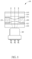
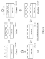
- FIG. 1 is a diagram illustrating a projector 100 according to a first embodiment of the present invention.
- the projector 100 comprises a laser module 110 and a wafer-level optics, where the wafer-level optics comprises a substrate 120, a collimator lens 122 imprinted on a surface of the substrate 120, a substrate 130, a collimator lens 132 imprinted on a surface of the substrate 130, a diffractive optical element (DOE) 140 imprinted on another surface of the substrate 130, and spacers 1 50.
- the projector 100 is arranged to project an image with a special pattern, and the projector 100 is positioned in an electronic device such as a smart phone or a pad.
- the laser module 110 is arranged to generate a laser beam, and particularly, the laser beam is an infrared light.
- the collimator lenses 122 and 132 are convex lenses, and are arranged to receive the laser beam from the laser module 110 to generate a collimated laser beam (parallel rays), where the collimated laser beam is substantially perpendicular to the surface of the substrate 1 30 and the DOE 140.
- the DOE 140 can serve as a pattern generator, and the collimated laser beam directly passes through the DOE 140 to generate a projected image, where the projected image may have a special pattern set by the DOE 140.
- the laser beam directly passes through the collimator lenses 122 and 132 and the DOE 140 to become the projected image having the special pattern, and the laser beam is not directed by any prism or any other reflective/refractive element.
- the projector 100 has a low thickness, and is allowed to be positioned in the thinner electronic device.
- FIG. 2 is a diagram illustrating a projector 200 according to a second embodiment of the present invention.
- the projector 200 comprises a laser module 210 and a wafer-level optics, where the wafer-level optics comprises a substrate 220, a concave collimator lens 222 imprinted on a surface of the substrate 220, a substrate 230, a convex collimator lens 232 imprinted on a surface of the substrate 230, a DOE 240 imprinted on another surface of the substrate 230, and spacers 250.
- the projector 200 is similar to the projector 100 shown in FIG. 1 but the collimator lens 222 is a concave lens.
- the collimator lens 222 can be a convex lens while the collimator lens 232 is a concave lens.
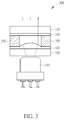
- FIG. 3 is a diagram illustrating a projector 300 according to a third embodiment of the present invention.
- the projector 300 comprises a laser module 310 and a wafer-level optics, where the wafer-level optics comprises a substrate 320, a convex collimator lens 322 imprinted on a surface of the substrate 320, a substrate 330, a DOE 340 imprinted on a surface of the substrate 330, and spacers 350.
- the projector 300 is similar to the projector 100 shown in FIG. 1 but no collimator lens is manufacturing on a surface of the substrate 330.
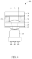
- FIG. 4 is a diagram illustrating a projector 400 according to a fourth embodiment of the present invention.
- the projector 400 comprises a laser module 410 and a wafer-level optics, where the wafer-level optics comprises a substrate 420, a convex collimator lens 422 imprinted on a surface of the substrate 420, another convex collimator lens 424 imprinted on another surface of the substrate 420, a substrate 430, a DOE 440 imprinted on a surface of the substrate 430, and spacers 450.
- the projector 400 is similar to the projector 300 shown in FIG. 3 but two collimator lenses 422 and 424 are manufacturing on two opposite surfaces of the substrate 430.
- the one of the collimator lenses 422 and 424 can be a convex lens while the other one of the collimator lenses 422 and 424 is a concave lens.
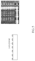
- the DOEs 140/240/340/440 are manufactured by nanoimprint semiconductor lithography.
- FIG. 5 shows a side view and a top view of part of the DOEs 140/240/340/440 according to one embodiment of the present invention.
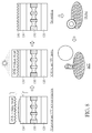
- FIGs. 6-8 show a manufacturing method of the wafer-level optics shown in FIG. 1 according to one embodiment of the present invention.
- FIG. 6 shows the details of imprinting the collimator lenses 122 and 132 on the substrates 1 20 and 130, respectively.
- the substrate 120/130 is cleaned for further process.
- an ultraviolet (UV) curable polymer is injected or dispensed on a surface of the substrate 120/130, and a working stamp is used to shape the UV curable polymer.
- an ultraviolet ray is used to cure the UV curable polymer, wherein the cured layer serves as the collimator lens 122/132.
- the working stamp is removed.
- edge residue removing and cleaning step is performed.
- an automated optical inspection AOI
- AOI automated optical inspection
- FIG. 7 shows details of assembling the substrates 120 and 130.
- the substrate 130 is bonded with the spacers 1 50.
- the substrate 120 is assembled with the substrate 130 via the spacers 1 50.
- a modulation transfer function (MTF) test is performed to inspect the image performance of the lenses.
- FIG. 8 shows details of imprinting the DOE 140 and the following assembling steps.
- the UV curable polymer is injected or dispensed on the surface of the substrate 130, and a DOE working stamp is used to shape the UV curable polymer by using the CCD alignment system.
- the ultraviolet ray is used to cure the UV curable polymer, wherein the cured layer serves as the DOE 140.
- the DOE working stamp is removed.
- the assembled device is diced into a plurality of squares, where each square serves as the wafer-level optics shown in FIG. 1 .
- the AOI is used to scan the substrate 120/130 under test for both catastrophic failure and quality defects.
- the squares i.e. the plurality of wafer-level optics
- the squares are sorted for further process.
- FIGs. 2-4 can be manufactured by the steps that are similar to the steps shown in FIGs. 6-8 . Because a person skilled in the art should understand the manufacturing steps of the embodiments shown in FIGs. 2-4 after reading the above-mentioned disclosure, further descriptions are omitted here.
- FIG. 9 is a diagram illustrating an electronic device 900 according to one embodiment of the present invention.
- the electronic device 900 is a smart phone, and the electronic device 900 comprises a projector 910, a camera module 920 and a processor 930.
- the projector 910 can be implemented by any one of the projector shown in FIGs. 1-4 , and the projector 910 is embedded in a back side of the electronic device 900, and is used to project an infrared image with a special pattern to a region of a surrounding environment.
- the camera module 920 captures the region of the surrounding environment to generate image data.
- the processor 930 analyzes the image data to obtain depth information of the image data.
- the electronic device 900 can simply generate a 3D image by using the projector 920 and only one camera module 930.
- the thickness of the projector is low enough to be embedded into a thinner electronic device.
- the electronic device can build a 3D image by merely analyzing an image captured by one camera module. Hence, the manufacturing cost and the loading of the processor can be improved.
Landscapes
- Physics & Mathematics (AREA)
- General Physics & Mathematics (AREA)
- Optics & Photonics (AREA)
- Engineering & Computer Science (AREA)
- Multimedia (AREA)
- Signal Processing (AREA)
- Computer Vision & Pattern Recognition (AREA)
- Manufacturing & Machinery (AREA)
- Projection Apparatus (AREA)
- Diffracting Gratings Or Hologram Optical Elements (AREA)
- Microscoopes, Condenser (AREA)
Applications Claiming Priority (1)
| Application Number | Priority Date | Filing Date | Title |
|---|---|---|---|
| US201562271354P | 2015-12-28 | 2015-12-28 |
Publications (1)
| Publication Number | Publication Date |
|---|---|
| EP3200000A1 true EP3200000A1 (de) | 2017-08-02 |
Family
ID=56296534
Family Applications (1)
| Application Number | Title | Priority Date | Filing Date |
|---|---|---|---|
| EP16176441.0A Withdrawn EP3200000A1 (de) | 2015-12-28 | 2016-06-27 | Projektor, elektronische vorrichtung mit dem projektor und zugehöriges herstellungsverfahren |
Country Status (6)
| Country | Link |
|---|---|
| US (2) | US20170187997A1 (de) |
| EP (1) | EP3200000A1 (de) |
| JP (1) | JP2017120364A (de) |
| KR (1) | KR20170077761A (de) |
| CN (1) | CN106918977A (de) |
| TW (1) | TWI621904B (de) |
Families Citing this family (24)
| Publication number | Priority date | Publication date | Assignee | Title |
|---|---|---|---|---|
| US10241244B2 (en) | 2016-07-29 | 2019-03-26 | Lumentum Operations Llc | Thin film total internal reflection diffraction grating for single polarization or dual polarization |
| US10466576B2 (en) * | 2017-10-20 | 2019-11-05 | Himax Technologies Limited | Method for controlling projector and associated electronic device |
| CN109839792B (zh) * | 2017-11-25 | 2024-05-03 | 宁波舜宇光电信息有限公司 | 具备编码光的结构光投影装置、电子设备及其应用 |
| US10841547B2 (en) * | 2018-01-09 | 2020-11-17 | Himax Technologies Limited | Method for fabricating small right angle prism mirrors involving 3D shape on optical glue layer |
| CN110068983A (zh) * | 2018-01-24 | 2019-07-30 | 宁波舜宇光电信息有限公司 | 结构光投影装置 |
| CN108255000A (zh) * | 2018-01-26 | 2018-07-06 | 深圳奥比中光科技有限公司 | 含有晶圆透镜的光学投影装置 |
| CN108181777A (zh) * | 2018-02-27 | 2018-06-19 | 广东欧珀移动通信有限公司 | 激光投射模组、深度相机及电子装置 |
| CN108344377B (zh) * | 2018-03-12 | 2020-05-15 | Oppo广东移动通信有限公司 | 激光投射模组、深度相机和电子装置 |
| US10962870B2 (en) * | 2018-03-12 | 2021-03-30 | Guangdong Oppo Mobile Telecommunications Corp., Ltd. | Laser projection unit, depth camera and electronic device |
| CN108535828A (zh) * | 2018-03-12 | 2018-09-14 | 广东欧珀移动通信有限公司 | 衍射光学组件、激光投射模组、深度相机及电子装置 |
| NL2020697B1 (en) * | 2018-03-30 | 2019-10-07 | Anteryon Wafer Optics B V | optical module |
| CN108594562A (zh) * | 2018-04-02 | 2018-09-28 | 浙江舜宇光学有限公司 | 投射模组及投影方法 |
| CN108646425B (zh) * | 2018-04-03 | 2019-08-23 | Oppo广东移动通信有限公司 | 激光投射器、图像获取装置及电子设备 |
| WO2019201010A1 (zh) | 2018-04-16 | 2019-10-24 | Oppo广东移动通信有限公司 | 激光投射器、相机模组和电子装置 |
| US10714891B2 (en) | 2018-07-06 | 2020-07-14 | Himax Technologies Limited | Projector, electronic device having projector and associated manufacturing method |
| TWI657264B (zh) * | 2018-07-19 | 2019-04-21 | 香港商印芯科技股份有限公司 | 結構光投射裝置 |
| US10802382B2 (en) * | 2018-07-24 | 2020-10-13 | Qualcomm Incorporated | Adjustable light projector for flood illumination and active depth sensing |
| JP2020020861A (ja) * | 2018-07-30 | 2020-02-06 | 奇景光電股▲ふん▼有限公司 | プロジェクタ、プロジェクタを有する電子機器及び関連する製造方法 |
| KR102146361B1 (ko) * | 2018-08-01 | 2020-08-21 | 하이맥스 테크놀로지스 리미티드 | 프로젝터, 프로젝터를 가진 전자 장치 및 관련 제조 방법 |
| US11223816B2 (en) * | 2018-09-26 | 2022-01-11 | Himax Technologies Limited | Multi-image projector and electronic device having multi-image projector |
| US10942429B2 (en) * | 2018-10-01 | 2021-03-09 | Himax Technologies Limited | Projector, electronic device having projector and associated control method |
| WO2020080169A1 (ja) | 2018-10-15 | 2020-04-23 | Agc株式会社 | 回折光学素子および照明光学系 |
| CN109708588A (zh) * | 2019-01-14 | 2019-05-03 | 业成科技(成都)有限公司 | 结构光投射器及结构光深度感测器 |
| CN114859446B (zh) * | 2022-06-14 | 2023-06-02 | 深圳迈塔兰斯科技有限公司 | 复合超透镜及其形成方法和点阵投影系统 |
Citations (4)
| Publication number | Priority date | Publication date | Assignee | Title |
|---|---|---|---|---|
| US20110188054A1 (en) * | 2010-02-02 | 2011-08-04 | Primesense Ltd | Integrated photonics module for optical projection |
| US20130038881A1 (en) * | 2011-08-09 | 2013-02-14 | Primesense Ltd. | Projectors of Structured Light |
| WO2014036680A1 (zh) * | 2012-09-04 | 2014-03-13 | 神画科技(深圳)有限公司 | 一种互动手机 |
| US20140293011A1 (en) * | 2013-03-28 | 2014-10-02 | Phasica, LLC | Scanner System for Determining the Three Dimensional Shape of an Object and Method for Using |
Family Cites Families (16)
| Publication number | Priority date | Publication date | Assignee | Title |
|---|---|---|---|---|
| US5718496A (en) * | 1996-06-25 | 1998-02-17 | Digital Optics Corporation | Projection pointer |
| US7610224B2 (en) * | 2001-11-02 | 2009-10-27 | Amazon Technologies, Inc. | Delivering ordered items to an appropriate address |
| JP3863394B2 (ja) * | 2001-07-04 | 2006-12-27 | 住友電装株式会社 | ワイヤーハーネス配索用摺動部品 |
| JP4210070B2 (ja) * | 2002-03-29 | 2009-01-14 | シャープ株式会社 | マイクロレンズ基板の作製方法 |
| US7032652B2 (en) * | 2004-07-06 | 2006-04-25 | Augux Co., Ltd. | Structure of heat conductive plate |
| US8462292B2 (en) * | 2008-07-31 | 2013-06-11 | Rambus Delaware Llc | Optically transmissive substrates and light emitting assemblies and methods of making same, and methods of displaying images using the optically transmissive substrates and light emitting assemblies |
| US20100079453A1 (en) * | 2008-09-30 | 2010-04-01 | Liang-Gee Chen | 3D Depth Generation by Vanishing Line Detection |
| US7763841B1 (en) * | 2009-05-27 | 2010-07-27 | Microsoft Corporation | Optical component for a depth sensor |
| DE102009028255A1 (de) * | 2009-08-05 | 2011-02-10 | Evonik Degussa Gmbh | Mikrostrukturierte multifunktionale anorganische Coating-Additive zur Vermeidung von Fouling (Biofilmbewuchs) bei aquatischen Anwendungen |
| US20120021845A1 (en) * | 2010-07-22 | 2012-01-26 | Timothy Charles Slavik | Indoor putting training aid |
| JPWO2013146487A1 (ja) * | 2012-03-30 | 2015-12-10 | コニカミノルタ株式会社 | レンズアレイ、レンズアレイの製造方法及び光学素子の製造方法 |
| US9846353B2 (en) * | 2012-06-01 | 2017-12-19 | Intel Corporation | Projection device combining and modifing light beam cross sectional dimensions |
| US9297889B2 (en) * | 2012-08-14 | 2016-03-29 | Microsoft Technology Licensing, Llc | Illumination light projection for a depth camera |
| CN204271438U (zh) * | 2014-10-31 | 2015-04-15 | 高准精密工业股份有限公司 | 表面固定型衍射光学激光模组 |
| TWM509339U (zh) * | 2015-05-15 | 2015-09-21 | Everready Prec Ind Corp | 光學裝置及其發光裝置 |
| US9733485B2 (en) * | 2015-10-30 | 2017-08-15 | Himax Technologies Limited | Collimating lens |
-
2016
- 2016-06-02 JP JP2016110556A patent/JP2017120364A/ja active Pending
- 2016-06-07 KR KR1020160070536A patent/KR20170077761A/ko not_active Ceased
- 2016-06-27 EP EP16176441.0A patent/EP3200000A1/de not_active Withdrawn
- 2016-06-28 US US15/194,578 patent/US20170187997A1/en not_active Abandoned
- 2016-06-28 TW TW105120376A patent/TWI621904B/zh active
- 2016-07-05 CN CN201610525135.9A patent/CN106918977A/zh active Pending
-
2018
- 2018-05-14 US US15/978,207 patent/US20180262726A1/en not_active Abandoned
Patent Citations (4)
| Publication number | Priority date | Publication date | Assignee | Title |
|---|---|---|---|---|
| US20110188054A1 (en) * | 2010-02-02 | 2011-08-04 | Primesense Ltd | Integrated photonics module for optical projection |
| US20130038881A1 (en) * | 2011-08-09 | 2013-02-14 | Primesense Ltd. | Projectors of Structured Light |
| WO2014036680A1 (zh) * | 2012-09-04 | 2014-03-13 | 神画科技(深圳)有限公司 | 一种互动手机 |
| US20140293011A1 (en) * | 2013-03-28 | 2014-10-02 | Phasica, LLC | Scanner System for Determining the Three Dimensional Shape of an Object and Method for Using |
Also Published As
| Publication number | Publication date |
|---|---|
| US20180262726A1 (en) | 2018-09-13 |
| KR20170077761A (ko) | 2017-07-06 |
| JP2017120364A (ja) | 2017-07-06 |
| TW201723629A (zh) | 2017-07-01 |
| US20170187997A1 (en) | 2017-06-29 |
| TWI621904B (zh) | 2018-04-21 |
| CN106918977A (zh) | 2017-07-04 |
Similar Documents
| Publication | Publication Date | Title |
|---|---|---|
| EP3200000A1 (de) | Projektor, elektronische vorrichtung mit dem projektor und zugehöriges herstellungsverfahren | |
| Brückner et al. | Thin wafer-level camera lenses inspired by insect compound eyes | |
| CN102822656B (zh) | 偏心量测量方法 | |
| CN107430988B (zh) | 压印装置、压印方法和制造物品的方法 | |
| JP2011203792A (ja) | 撮像装置 | |
| CN116057473A (zh) | 同轴透视对准成像系统 | |
| US9349765B2 (en) | Suspended lens system having a non-zero optical transmission substrate facing the concave surface of a single-piece lens and wafer-level method for manufacturing the same | |
| KR101188202B1 (ko) | 프로젝션 디스플레이 장치의 광학계 | |
| US12165341B2 (en) | Optical resolution measurement method for optical devices | |
| JP5644765B2 (ja) | ウエハレンズの製造方法 | |
| KR20190124542A (ko) | 카메라 모듈 및 그의 깊이 정보 추출 방법 | |
| TWI507730B (zh) | The manufacturing method of optical box and optical module | |
| US9933601B2 (en) | Stacked wafer lens and camera | |
| CN109494244B (zh) | 带有光场相机的有机发光二极管显示面板 | |
| TWI579587B (zh) | 晶圓級透鏡系統及其製造方法 | |
| TWI584645B (zh) | 含有乾黏合劑層之光學組件及相關方法 | |
| Brückner et al. | Ultra-compact close-up microoptical imaging system | |
| CN108873302A (zh) | 一种光场显微图像的自动校正和重新聚焦方法 | |
| JP2018071990A (ja) | 多心光コネクタフェルールの偏心測定装置および方法 | |
| US20220308271A1 (en) | Optical element and manufacturing method for optical element | |
| JP6209903B2 (ja) | 検査方法、ナノインプリント用モールド製造方法、ナノインプリント方法、および、検査装置 | |
| Brückner et al. | A multi-aperture approach to wafer-level camera lenses | |
| JP2012231465A (ja) | 複数のイメージセンサーを有するスキャナーのイメージ生成方法及びイメージ生成システム | |
| TWM555478U (zh) | 成像模組及取像裝置 | |
| Bräuer et al. | High resolution multichannel imaging systems |
Legal Events
| Date | Code | Title | Description |
|---|---|---|---|
| PUAI | Public reference made under article 153(3) epc to a published international application that has entered the european phase |
Free format text: ORIGINAL CODE: 0009012 |
|
| AK | Designated contracting states |
Kind code of ref document: A1 Designated state(s): AL AT BE BG CH CY CZ DE DK EE ES FI FR GB GR HR HU IE IS IT LI LT LU LV MC MK MT NL NO PL PT RO RS SE SI SK SM TR |
|
| AX | Request for extension of the european patent |
Extension state: BA ME |
|
| STAA | Information on the status of an ep patent application or granted ep patent |
Free format text: STATUS: THE APPLICATION IS DEEMED TO BE WITHDRAWN |
|
| 18D | Application deemed to be withdrawn |
Effective date: 20180203 |