EP3176812A1 - Halbleiterbauelement und verfahren zur herstellung solch eines halbleiterbauelements - Google Patents
Halbleiterbauelement und verfahren zur herstellung solch eines halbleiterbauelements Download PDFInfo
- Publication number
- EP3176812A1 EP3176812A1 EP15197558.8A EP15197558A EP3176812A1 EP 3176812 A1 EP3176812 A1 EP 3176812A1 EP 15197558 A EP15197558 A EP 15197558A EP 3176812 A1 EP3176812 A1 EP 3176812A1
- Authority
- EP
- European Patent Office
- Prior art keywords
- layer
- doping concentration
- well
- plug
- mask
- Prior art date
- Legal status (The legal status is an assumption and is not a legal conclusion. Google has not performed a legal analysis and makes no representation as to the accuracy of the status listed.)
- Withdrawn
Links
- 239000004065 semiconductor Substances 0.000 title claims abstract description 35
- 238000004519 manufacturing process Methods 0.000 title claims description 31
- 238000000034 method Methods 0.000 title description 19
- 239000002019 doping agent Substances 0.000 claims description 41
- 239000000758 substrate Substances 0.000 claims description 29
- 238000005530 etching Methods 0.000 claims description 11
- 229910044991 metal oxide Inorganic materials 0.000 claims description 3
- 150000004706 metal oxides Chemical class 0.000 claims description 3
- 230000005669 field effect Effects 0.000 claims description 2
- 239000000463 material Substances 0.000 description 14
- 229910021420 polycrystalline silicon Inorganic materials 0.000 description 12
- 230000008569 process Effects 0.000 description 12
- 230000005684 electric field Effects 0.000 description 11
- 230000015556 catabolic process Effects 0.000 description 5
- 230000000694 effects Effects 0.000 description 5
- HBMJWWWQQXIZIP-UHFFFAOYSA-N silicon carbide Chemical compound [Si+]#[C-] HBMJWWWQQXIZIP-UHFFFAOYSA-N 0.000 description 5
- 230000000903 blocking effect Effects 0.000 description 4
- 230000008021 deposition Effects 0.000 description 4
- 238000002513 implantation Methods 0.000 description 4
- 230000003647 oxidation Effects 0.000 description 4
- 238000007254 oxidation reaction Methods 0.000 description 4
- 229910010271 silicon carbide Inorganic materials 0.000 description 4
- 229910052782 aluminium Inorganic materials 0.000 description 3
- 229910052796 boron Inorganic materials 0.000 description 3
- 230000003071 parasitic effect Effects 0.000 description 3
- 230000035515 penetration Effects 0.000 description 3
- 125000006850 spacer group Chemical group 0.000 description 3
- ZOXJGFHDIHLPTG-UHFFFAOYSA-N Boron Chemical compound [B] ZOXJGFHDIHLPTG-UHFFFAOYSA-N 0.000 description 2
- XAGFODPZIPBFFR-UHFFFAOYSA-N aluminium Chemical compound [Al] XAGFODPZIPBFFR-UHFFFAOYSA-N 0.000 description 2
- 239000012212 insulator Substances 0.000 description 2
- 229910052751 metal Inorganic materials 0.000 description 2
- 239000002184 metal Substances 0.000 description 2
- 230000002028 premature Effects 0.000 description 2
- 229910002601 GaN Inorganic materials 0.000 description 1
- JMASRVWKEDWRBT-UHFFFAOYSA-N Gallium nitride Chemical compound [Ga]#N JMASRVWKEDWRBT-UHFFFAOYSA-N 0.000 description 1
- 229910052581 Si3N4 Inorganic materials 0.000 description 1
- XUIMIQQOPSSXEZ-UHFFFAOYSA-N Silicon Chemical compound [Si] XUIMIQQOPSSXEZ-UHFFFAOYSA-N 0.000 description 1
- 230000004913 activation Effects 0.000 description 1
- 230000015572 biosynthetic process Effects 0.000 description 1
- 239000005380 borophosphosilicate glass Substances 0.000 description 1
- 239000004020 conductor Substances 0.000 description 1
- 230000007423 decrease Effects 0.000 description 1
- 230000003247 decreasing effect Effects 0.000 description 1
- 230000001419 dependent effect Effects 0.000 description 1
- 229910003460 diamond Inorganic materials 0.000 description 1
- 239000010432 diamond Substances 0.000 description 1
- 239000003989 dielectric material Substances 0.000 description 1
- 230000003467 diminishing effect Effects 0.000 description 1
- 239000011810 insulating material Substances 0.000 description 1
- 230000000873 masking effect Effects 0.000 description 1
- 230000001590 oxidative effect Effects 0.000 description 1
- 230000009467 reduction Effects 0.000 description 1
- 230000002441 reversible effect Effects 0.000 description 1
- 239000005368 silicate glass Substances 0.000 description 1
- 229910052710 silicon Inorganic materials 0.000 description 1
- 239000010703 silicon Substances 0.000 description 1
- HQVNEWCFYHHQES-UHFFFAOYSA-N silicon nitride Chemical compound N12[Si]34N5[Si]62N3[Si]51N64 HQVNEWCFYHHQES-UHFFFAOYSA-N 0.000 description 1
Images


Classifications
-
- H—ELECTRICITY
- H01—ELECTRIC ELEMENTS
- H01L—SEMICONDUCTOR DEVICES NOT COVERED BY CLASS H10
- H01L21/00—Processes or apparatus adapted for the manufacture or treatment of semiconductor or solid state devices or of parts thereof
- H01L21/02—Manufacture or treatment of semiconductor devices or of parts thereof
- H01L21/04—Manufacture or treatment of semiconductor devices or of parts thereof the devices having at least one potential-jump barrier or surface barrier, e.g. PN junction, depletion layer or carrier concentration layer
- H01L21/18—Manufacture or treatment of semiconductor devices or of parts thereof the devices having at least one potential-jump barrier or surface barrier, e.g. PN junction, depletion layer or carrier concentration layer the devices having semiconductor bodies comprising elements of Group IV of the Periodic System or AIIIBV compounds with or without impurities, e.g. doping materials
- H01L21/26—Bombardment with radiation
- H01L21/263—Bombardment with radiation with high-energy radiation
- H01L21/265—Bombardment with radiation with high-energy radiation producing ion implantation
- H01L21/266—Bombardment with radiation with high-energy radiation producing ion implantation using masks
-
- H—ELECTRICITY
- H01—ELECTRIC ELEMENTS
- H01L—SEMICONDUCTOR DEVICES NOT COVERED BY CLASS H10
- H01L21/00—Processes or apparatus adapted for the manufacture or treatment of semiconductor or solid state devices or of parts thereof
- H01L21/02—Manufacture or treatment of semiconductor devices or of parts thereof
- H01L21/04—Manufacture or treatment of semiconductor devices or of parts thereof the devices having at least one potential-jump barrier or surface barrier, e.g. PN junction, depletion layer or carrier concentration layer
- H01L21/0445—Manufacture or treatment of semiconductor devices or of parts thereof the devices having at least one potential-jump barrier or surface barrier, e.g. PN junction, depletion layer or carrier concentration layer the devices having semiconductor bodies comprising crystalline silicon carbide
- H01L21/0455—Making n or p doped regions or layers, e.g. using diffusion
- H01L21/046—Making n or p doped regions or layers, e.g. using diffusion using ion implantation
- H01L21/0465—Making n or p doped regions or layers, e.g. using diffusion using ion implantation using masks
-
- H—ELECTRICITY
- H01—ELECTRIC ELEMENTS
- H01L—SEMICONDUCTOR DEVICES NOT COVERED BY CLASS H10
- H01L21/00—Processes or apparatus adapted for the manufacture or treatment of semiconductor or solid state devices or of parts thereof
- H01L21/02—Manufacture or treatment of semiconductor devices or of parts thereof
- H01L21/04—Manufacture or treatment of semiconductor devices or of parts thereof the devices having at least one potential-jump barrier or surface barrier, e.g. PN junction, depletion layer or carrier concentration layer
- H01L21/0445—Manufacture or treatment of semiconductor devices or of parts thereof the devices having at least one potential-jump barrier or surface barrier, e.g. PN junction, depletion layer or carrier concentration layer the devices having semiconductor bodies comprising crystalline silicon carbide
- H01L21/048—Making electrodes
- H01L21/0485—Ohmic electrodes
-
- H—ELECTRICITY
- H01—ELECTRIC ELEMENTS
- H01L—SEMICONDUCTOR DEVICES NOT COVERED BY CLASS H10
- H01L21/00—Processes or apparatus adapted for the manufacture or treatment of semiconductor or solid state devices or of parts thereof
- H01L21/02—Manufacture or treatment of semiconductor devices or of parts thereof
- H01L21/04—Manufacture or treatment of semiconductor devices or of parts thereof the devices having at least one potential-jump barrier or surface barrier, e.g. PN junction, depletion layer or carrier concentration layer
- H01L21/0445—Manufacture or treatment of semiconductor devices or of parts thereof the devices having at least one potential-jump barrier or surface barrier, e.g. PN junction, depletion layer or carrier concentration layer the devices having semiconductor bodies comprising crystalline silicon carbide
- H01L21/048—Making electrodes
- H01L21/049—Conductor-insulator-semiconductor electrodes, e.g. MIS contacts
-
- H—ELECTRICITY
- H01—ELECTRIC ELEMENTS
- H01L—SEMICONDUCTOR DEVICES NOT COVERED BY CLASS H10
- H01L29/00—Semiconductor devices adapted for rectifying, amplifying, oscillating or switching, or capacitors or resistors with at least one potential-jump barrier or surface barrier, e.g. PN junction depletion layer or carrier concentration layer; Details of semiconductor bodies or of electrodes thereof ; Multistep manufacturing processes therefor
- H01L29/02—Semiconductor bodies ; Multistep manufacturing processes therefor
- H01L29/06—Semiconductor bodies ; Multistep manufacturing processes therefor characterised by their shape; characterised by the shapes, relative sizes, or dispositions of the semiconductor regions ; characterised by the concentration or distribution of impurities within semiconductor regions
- H01L29/0603—Semiconductor bodies ; Multistep manufacturing processes therefor characterised by their shape; characterised by the shapes, relative sizes, or dispositions of the semiconductor regions ; characterised by the concentration or distribution of impurities within semiconductor regions characterised by particular constructional design considerations, e.g. for preventing surface leakage, for controlling electric field concentration or for internal isolations regions
- H01L29/0607—Semiconductor bodies ; Multistep manufacturing processes therefor characterised by their shape; characterised by the shapes, relative sizes, or dispositions of the semiconductor regions ; characterised by the concentration or distribution of impurities within semiconductor regions characterised by particular constructional design considerations, e.g. for preventing surface leakage, for controlling electric field concentration or for internal isolations regions for preventing surface leakage or controlling electric field concentration
- H01L29/0611—Semiconductor bodies ; Multistep manufacturing processes therefor characterised by their shape; characterised by the shapes, relative sizes, or dispositions of the semiconductor regions ; characterised by the concentration or distribution of impurities within semiconductor regions characterised by particular constructional design considerations, e.g. for preventing surface leakage, for controlling electric field concentration or for internal isolations regions for preventing surface leakage or controlling electric field concentration for increasing or controlling the breakdown voltage of reverse biased devices
- H01L29/0615—Semiconductor bodies ; Multistep manufacturing processes therefor characterised by their shape; characterised by the shapes, relative sizes, or dispositions of the semiconductor regions ; characterised by the concentration or distribution of impurities within semiconductor regions characterised by particular constructional design considerations, e.g. for preventing surface leakage, for controlling electric field concentration or for internal isolations regions for preventing surface leakage or controlling electric field concentration for increasing or controlling the breakdown voltage of reverse biased devices by the doping profile or the shape or the arrangement of the PN junction, or with supplementary regions, e.g. junction termination extension [JTE]
- H01L29/063—Reduced surface field [RESURF] pn-junction structures
- H01L29/0634—Multiple reduced surface field (multi-RESURF) structures, e.g. double RESURF, charge compensation, cool, superjunction (SJ), 3D-RESURF, composite buffer (CB) structures
-
- H—ELECTRICITY
- H01—ELECTRIC ELEMENTS
- H01L—SEMICONDUCTOR DEVICES NOT COVERED BY CLASS H10
- H01L29/00—Semiconductor devices adapted for rectifying, amplifying, oscillating or switching, or capacitors or resistors with at least one potential-jump barrier or surface barrier, e.g. PN junction depletion layer or carrier concentration layer; Details of semiconductor bodies or of electrodes thereof ; Multistep manufacturing processes therefor
- H01L29/02—Semiconductor bodies ; Multistep manufacturing processes therefor
- H01L29/06—Semiconductor bodies ; Multistep manufacturing processes therefor characterised by their shape; characterised by the shapes, relative sizes, or dispositions of the semiconductor regions ; characterised by the concentration or distribution of impurities within semiconductor regions
- H01L29/0684—Semiconductor bodies ; Multistep manufacturing processes therefor characterised by their shape; characterised by the shapes, relative sizes, or dispositions of the semiconductor regions ; characterised by the concentration or distribution of impurities within semiconductor regions characterised by the shape, relative sizes or dispositions of the semiconductor regions or junctions between the regions
- H01L29/0692—Surface layout
- H01L29/0696—Surface layout of cellular field-effect devices, e.g. multicellular DMOS transistors or IGBTs
-
- H—ELECTRICITY
- H01—ELECTRIC ELEMENTS
- H01L—SEMICONDUCTOR DEVICES NOT COVERED BY CLASS H10
- H01L29/00—Semiconductor devices adapted for rectifying, amplifying, oscillating or switching, or capacitors or resistors with at least one potential-jump barrier or surface barrier, e.g. PN junction depletion layer or carrier concentration layer; Details of semiconductor bodies or of electrodes thereof ; Multistep manufacturing processes therefor
- H01L29/02—Semiconductor bodies ; Multistep manufacturing processes therefor
- H01L29/06—Semiconductor bodies ; Multistep manufacturing processes therefor characterised by their shape; characterised by the shapes, relative sizes, or dispositions of the semiconductor regions ; characterised by the concentration or distribution of impurities within semiconductor regions
- H01L29/08—Semiconductor bodies ; Multistep manufacturing processes therefor characterised by their shape; characterised by the shapes, relative sizes, or dispositions of the semiconductor regions ; characterised by the concentration or distribution of impurities within semiconductor regions with semiconductor regions connected to an electrode carrying current to be rectified, amplified or switched and such electrode being part of a semiconductor device which comprises three or more electrodes
- H01L29/0821—Collector regions of bipolar transistors
-
- H—ELECTRICITY
- H01—ELECTRIC ELEMENTS
- H01L—SEMICONDUCTOR DEVICES NOT COVERED BY CLASS H10
- H01L29/00—Semiconductor devices adapted for rectifying, amplifying, oscillating or switching, or capacitors or resistors with at least one potential-jump barrier or surface barrier, e.g. PN junction depletion layer or carrier concentration layer; Details of semiconductor bodies or of electrodes thereof ; Multistep manufacturing processes therefor
- H01L29/02—Semiconductor bodies ; Multistep manufacturing processes therefor
- H01L29/06—Semiconductor bodies ; Multistep manufacturing processes therefor characterised by their shape; characterised by the shapes, relative sizes, or dispositions of the semiconductor regions ; characterised by the concentration or distribution of impurities within semiconductor regions
- H01L29/08—Semiconductor bodies ; Multistep manufacturing processes therefor characterised by their shape; characterised by the shapes, relative sizes, or dispositions of the semiconductor regions ; characterised by the concentration or distribution of impurities within semiconductor regions with semiconductor regions connected to an electrode carrying current to be rectified, amplified or switched and such electrode being part of a semiconductor device which comprises three or more electrodes
- H01L29/0843—Source or drain regions of field-effect devices
- H01L29/0847—Source or drain regions of field-effect devices of field-effect transistors with insulated gate
- H01L29/0852—Source or drain regions of field-effect devices of field-effect transistors with insulated gate of DMOS transistors
- H01L29/0856—Source regions
- H01L29/086—Impurity concentration or distribution
-
- H—ELECTRICITY
- H01—ELECTRIC ELEMENTS
- H01L—SEMICONDUCTOR DEVICES NOT COVERED BY CLASS H10
- H01L29/00—Semiconductor devices adapted for rectifying, amplifying, oscillating or switching, or capacitors or resistors with at least one potential-jump barrier or surface barrier, e.g. PN junction depletion layer or carrier concentration layer; Details of semiconductor bodies or of electrodes thereof ; Multistep manufacturing processes therefor
- H01L29/02—Semiconductor bodies ; Multistep manufacturing processes therefor
- H01L29/06—Semiconductor bodies ; Multistep manufacturing processes therefor characterised by their shape; characterised by the shapes, relative sizes, or dispositions of the semiconductor regions ; characterised by the concentration or distribution of impurities within semiconductor regions
- H01L29/08—Semiconductor bodies ; Multistep manufacturing processes therefor characterised by their shape; characterised by the shapes, relative sizes, or dispositions of the semiconductor regions ; characterised by the concentration or distribution of impurities within semiconductor regions with semiconductor regions connected to an electrode carrying current to be rectified, amplified or switched and such electrode being part of a semiconductor device which comprises three or more electrodes
- H01L29/0843—Source or drain regions of field-effect devices
- H01L29/0847—Source or drain regions of field-effect devices of field-effect transistors with insulated gate
- H01L29/0852—Source or drain regions of field-effect devices of field-effect transistors with insulated gate of DMOS transistors
- H01L29/0856—Source regions
- H01L29/0865—Disposition
-
- H—ELECTRICITY
- H01—ELECTRIC ELEMENTS
- H01L—SEMICONDUCTOR DEVICES NOT COVERED BY CLASS H10
- H01L29/00—Semiconductor devices adapted for rectifying, amplifying, oscillating or switching, or capacitors or resistors with at least one potential-jump barrier or surface barrier, e.g. PN junction depletion layer or carrier concentration layer; Details of semiconductor bodies or of electrodes thereof ; Multistep manufacturing processes therefor
- H01L29/02—Semiconductor bodies ; Multistep manufacturing processes therefor
- H01L29/06—Semiconductor bodies ; Multistep manufacturing processes therefor characterised by their shape; characterised by the shapes, relative sizes, or dispositions of the semiconductor regions ; characterised by the concentration or distribution of impurities within semiconductor regions
- H01L29/10—Semiconductor bodies ; Multistep manufacturing processes therefor characterised by their shape; characterised by the shapes, relative sizes, or dispositions of the semiconductor regions ; characterised by the concentration or distribution of impurities within semiconductor regions with semiconductor regions connected to an electrode not carrying current to be rectified, amplified or switched and such electrode being part of a semiconductor device which comprises three or more electrodes
- H01L29/1025—Channel region of field-effect devices
- H01L29/1029—Channel region of field-effect devices of field-effect transistors
- H01L29/1033—Channel region of field-effect devices of field-effect transistors with insulated gate, e.g. characterised by the length, the width, the geometric contour or the doping structure
-
- H—ELECTRICITY
- H01—ELECTRIC ELEMENTS
- H01L—SEMICONDUCTOR DEVICES NOT COVERED BY CLASS H10
- H01L29/00—Semiconductor devices adapted for rectifying, amplifying, oscillating or switching, or capacitors or resistors with at least one potential-jump barrier or surface barrier, e.g. PN junction depletion layer or carrier concentration layer; Details of semiconductor bodies or of electrodes thereof ; Multistep manufacturing processes therefor
- H01L29/02—Semiconductor bodies ; Multistep manufacturing processes therefor
- H01L29/06—Semiconductor bodies ; Multistep manufacturing processes therefor characterised by their shape; characterised by the shapes, relative sizes, or dispositions of the semiconductor regions ; characterised by the concentration or distribution of impurities within semiconductor regions
- H01L29/10—Semiconductor bodies ; Multistep manufacturing processes therefor characterised by their shape; characterised by the shapes, relative sizes, or dispositions of the semiconductor regions ; characterised by the concentration or distribution of impurities within semiconductor regions with semiconductor regions connected to an electrode not carrying current to be rectified, amplified or switched and such electrode being part of a semiconductor device which comprises three or more electrodes
- H01L29/1095—Body region, i.e. base region, of DMOS transistors or IGBTs
-
- H—ELECTRICITY
- H01—ELECTRIC ELEMENTS
- H01L—SEMICONDUCTOR DEVICES NOT COVERED BY CLASS H10
- H01L29/00—Semiconductor devices adapted for rectifying, amplifying, oscillating or switching, or capacitors or resistors with at least one potential-jump barrier or surface barrier, e.g. PN junction depletion layer or carrier concentration layer; Details of semiconductor bodies or of electrodes thereof ; Multistep manufacturing processes therefor
- H01L29/02—Semiconductor bodies ; Multistep manufacturing processes therefor
- H01L29/12—Semiconductor bodies ; Multistep manufacturing processes therefor characterised by the materials of which they are formed
- H01L29/16—Semiconductor bodies ; Multistep manufacturing processes therefor characterised by the materials of which they are formed including, apart from doping materials or other impurities, only elements of Group IV of the Periodic System
- H01L29/1608—Silicon carbide
-
- H—ELECTRICITY
- H01—ELECTRIC ELEMENTS
- H01L—SEMICONDUCTOR DEVICES NOT COVERED BY CLASS H10
- H01L29/00—Semiconductor devices adapted for rectifying, amplifying, oscillating or switching, or capacitors or resistors with at least one potential-jump barrier or surface barrier, e.g. PN junction depletion layer or carrier concentration layer; Details of semiconductor bodies or of electrodes thereof ; Multistep manufacturing processes therefor
- H01L29/02—Semiconductor bodies ; Multistep manufacturing processes therefor
- H01L29/36—Semiconductor bodies ; Multistep manufacturing processes therefor characterised by the concentration or distribution of impurities in the bulk material
-
- H—ELECTRICITY
- H01—ELECTRIC ELEMENTS
- H01L—SEMICONDUCTOR DEVICES NOT COVERED BY CLASS H10
- H01L29/00—Semiconductor devices adapted for rectifying, amplifying, oscillating or switching, or capacitors or resistors with at least one potential-jump barrier or surface barrier, e.g. PN junction depletion layer or carrier concentration layer; Details of semiconductor bodies or of electrodes thereof ; Multistep manufacturing processes therefor
- H01L29/66—Types of semiconductor device ; Multistep manufacturing processes therefor
- H01L29/66007—Multistep manufacturing processes
- H01L29/66053—Multistep manufacturing processes of devices having a semiconductor body comprising crystalline silicon carbide
- H01L29/66068—Multistep manufacturing processes of devices having a semiconductor body comprising crystalline silicon carbide the devices being controllable only by the electric current supplied or the electric potential applied, to an electrode which does not carry the current to be rectified, amplified or switched, e.g. three-terminal devices
-
- H—ELECTRICITY
- H01—ELECTRIC ELEMENTS
- H01L—SEMICONDUCTOR DEVICES NOT COVERED BY CLASS H10
- H01L29/00—Semiconductor devices adapted for rectifying, amplifying, oscillating or switching, or capacitors or resistors with at least one potential-jump barrier or surface barrier, e.g. PN junction depletion layer or carrier concentration layer; Details of semiconductor bodies or of electrodes thereof ; Multistep manufacturing processes therefor
- H01L29/66—Types of semiconductor device ; Multistep manufacturing processes therefor
- H01L29/66007—Multistep manufacturing processes
- H01L29/66075—Multistep manufacturing processes of devices having semiconductor bodies comprising group 14 or group 13/15 materials
- H01L29/66227—Multistep manufacturing processes of devices having semiconductor bodies comprising group 14 or group 13/15 materials the devices being controllable only by the electric current supplied or the electric potential applied, to an electrode which does not carry the current to be rectified, amplified or switched, e.g. three-terminal devices
- H01L29/66234—Bipolar junction transistors [BJT]
- H01L29/66325—Bipolar junction transistors [BJT] controlled by field-effect, e.g. insulated gate bipolar transistors [IGBT]
- H01L29/66333—Vertical insulated gate bipolar transistors
-
- H—ELECTRICITY
- H01—ELECTRIC ELEMENTS
- H01L—SEMICONDUCTOR DEVICES NOT COVERED BY CLASS H10
- H01L29/00—Semiconductor devices adapted for rectifying, amplifying, oscillating or switching, or capacitors or resistors with at least one potential-jump barrier or surface barrier, e.g. PN junction depletion layer or carrier concentration layer; Details of semiconductor bodies or of electrodes thereof ; Multistep manufacturing processes therefor
- H01L29/66—Types of semiconductor device ; Multistep manufacturing processes therefor
- H01L29/66007—Multistep manufacturing processes
- H01L29/66075—Multistep manufacturing processes of devices having semiconductor bodies comprising group 14 or group 13/15 materials
- H01L29/66227—Multistep manufacturing processes of devices having semiconductor bodies comprising group 14 or group 13/15 materials the devices being controllable only by the electric current supplied or the electric potential applied, to an electrode which does not carry the current to be rectified, amplified or switched, e.g. three-terminal devices
- H01L29/66409—Unipolar field-effect transistors
- H01L29/66477—Unipolar field-effect transistors with an insulated gate, i.e. MISFET
- H01L29/66674—DMOS transistors, i.e. MISFETs with a channel accommodating body or base region adjoining a drain drift region
- H01L29/66712—Vertical DMOS transistors, i.e. VDMOS transistors
-
- H—ELECTRICITY
- H01—ELECTRIC ELEMENTS
- H01L—SEMICONDUCTOR DEVICES NOT COVERED BY CLASS H10
- H01L29/00—Semiconductor devices adapted for rectifying, amplifying, oscillating or switching, or capacitors or resistors with at least one potential-jump barrier or surface barrier, e.g. PN junction depletion layer or carrier concentration layer; Details of semiconductor bodies or of electrodes thereof ; Multistep manufacturing processes therefor
- H01L29/66—Types of semiconductor device ; Multistep manufacturing processes therefor
- H01L29/68—Types of semiconductor device ; Multistep manufacturing processes therefor controllable by only the electric current supplied, or only the electric potential applied, to an electrode which does not carry the current to be rectified, amplified or switched
- H01L29/70—Bipolar devices
- H01L29/72—Transistor-type devices, i.e. able to continuously respond to applied control signals
- H01L29/739—Transistor-type devices, i.e. able to continuously respond to applied control signals controlled by field-effect, e.g. bipolar static induction transistors [BSIT]
- H01L29/7393—Insulated gate bipolar mode transistors, i.e. IGBT; IGT; COMFET
- H01L29/7395—Vertical transistors, e.g. vertical IGBT
-
- H—ELECTRICITY
- H01—ELECTRIC ELEMENTS
- H01L—SEMICONDUCTOR DEVICES NOT COVERED BY CLASS H10
- H01L29/00—Semiconductor devices adapted for rectifying, amplifying, oscillating or switching, or capacitors or resistors with at least one potential-jump barrier or surface barrier, e.g. PN junction depletion layer or carrier concentration layer; Details of semiconductor bodies or of electrodes thereof ; Multistep manufacturing processes therefor
- H01L29/66—Types of semiconductor device ; Multistep manufacturing processes therefor
- H01L29/68—Types of semiconductor device ; Multistep manufacturing processes therefor controllable by only the electric current supplied, or only the electric potential applied, to an electrode which does not carry the current to be rectified, amplified or switched
- H01L29/76—Unipolar devices, e.g. field effect transistors
- H01L29/772—Field effect transistors
- H01L29/78—Field effect transistors with field effect produced by an insulated gate
- H01L29/7801—DMOS transistors, i.e. MISFETs with a channel accommodating body or base region adjoining a drain drift region
- H01L29/7802—Vertical DMOS transistors, i.e. VDMOS transistors
- H01L29/7811—Vertical DMOS transistors, i.e. VDMOS transistors with an edge termination structure
-
- H—ELECTRICITY
- H01—ELECTRIC ELEMENTS
- H01L—SEMICONDUCTOR DEVICES NOT COVERED BY CLASS H10
- H01L29/00—Semiconductor devices adapted for rectifying, amplifying, oscillating or switching, or capacitors or resistors with at least one potential-jump barrier or surface barrier, e.g. PN junction depletion layer or carrier concentration layer; Details of semiconductor bodies or of electrodes thereof ; Multistep manufacturing processes therefor
- H01L29/02—Semiconductor bodies ; Multistep manufacturing processes therefor
- H01L29/12—Semiconductor bodies ; Multistep manufacturing processes therefor characterised by the materials of which they are formed
- H01L29/20—Semiconductor bodies ; Multistep manufacturing processes therefor characterised by the materials of which they are formed including, apart from doping materials or other impurities, only AIIIBV compounds
- H01L29/2003—Nitride compounds
Definitions
- the invention relates to the field of power electronics and more particularly to a method for manufacturing a semiconductor device and to such a semiconductor device.
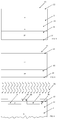
- FIG 17 a prior art MOSFET 100 is shown as known from US 7 074643 B2 .
- the prior art MOSFET 100 is made of an n+ silicon carbide (SiC) substrate 80 and comprises between a first main side 20 and a second main side 22 an n- doped drift layer 2.
- SiC silicon carbide
- a p++ doped contact layer 65 is arranged, which laterally extends to the source regions. Due to its high doping concentration the p++ doped contact layer provides a good ohmic contact to a first main electrode 9 (source electrode).
- the contact layer 65 is a shallow layer spatially (i.e. in depth direction, which direction is vertical to the first main side 20) extending to a contact layer depth 67, which is less deep than the well layers 5, 5', but electrically and mechanically contacting the well layers 5, 5' in order to connect the well layers 5, 5' to the source electrode 9.
- the contact layer 65 overlaps with the source regions 3, 3' the channel layers 4, 4', so that the contact layer 65 is the only p doped layer in contact with the first main electrode 9.
- a MOS (metal-oxide-semiconductor) cell is formed by the regions beforehand
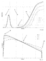
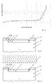
- the deep highly doped plug improves the contact to the well layer. Its depth is as least as great as the depth of the well layer to protect the channel layers of the MOS cell from peaks of the electric field, which are highest underneath the center of the MOS cell, i.e. below the location of the plug. This avoids undesired parasitic actions (parasitic transistor in case of a MOSFET and parasitic thyristor in case of an IGBT) as well as it diminishes short-channel effects (see FIG 22 ).
- FIG 22 it is shown that for a 300 nm wide channel (being the extension of the channel layer between the source region and the drift layer) the leakage current abruptly rises for forward blocking voltages smaller than the avalanche breakdown voltage, resulting in a premature breakdown of the device.
- breakdown can be shifted to higher forward blocking voltages.
- FIGs 18 to 21 show the electric fields through different planes of the MOS-cell of the device.
- the plug depth is given relative to the depth of the p well layer.
- Prior Art means that the plug is less deep than the p-well layer.
- D1 means that the plug and the p-well layer have the same depth.
- D2 shall mean that the plug depth is 1.5 times the well layer depth and "D3" means that the plug depth is two times larger than the well layer depth.
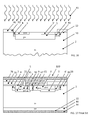
- FIG 18 shows the electric field from the first to the second main side between two MOS cells (cut along line A - - A in FIG 2 ).
- FIG 19 is a detail from FIG 18 at the interface between the first insulating layer 72 of the gate electrode 7 and the drift layer 2 (dotted area of FIG 18 ). From this figure it is obvious, that the electric field is reduced in the wide bandgap material as well as in the insulating layer of the gate electrode (e.g. gate oxide).
- FIG 20 shows the electric field in a plane parallel to the first main side (cut along line B - - B in FIG 2 ); showing the electric field in a non-depleted region 47 of the channel layer and in a depleted region 48 of the channel layer.
- FIG 21 shows the electric field along line C - - C in FIG 2 , which plane lies parallel to line A - - A and goes through the channel layer.
- FIG 1 shows an inventive insulated gate bipolar transistor (IGBT) 1.
- the IGBT 1 is a wide bandgap device, e.g. a silicon carbide device, comprising a lowly (n-) doped drift layer 2 between a first main side 20 and a second main side 22 of the device opposite to the first main side 20.
- Wide band gap materials shall be materials having a bandgap of at least 2 eV like silicon carbide, gallium nitride or diamond not excluding other wide bandgap materials.
- the doping concentration and thickness of the drift layer 2 are chosen.
- the drift layer 2 has a doping concentration between 1 * 10 12 and 1 * 10 17 cm -3 and a thickness between 1 to 500 ⁇ m. The thicknesses shall be measured in depth direction, i.e. in a direction vertical to the first main side 20.
- a p+ doped collector layer 8 is arranged on the second main side 22 and has exemplarily a doping concentration between 1 * 10 18 and 1 * 10 20 cm -3 .
- the collector layer 8 contacts a second main electrode 90, which is a collector electrode for an IGBT.
- an n doped buffer layer 25 may be arranged, which has a higher doping concentration than the drift layer 2 (shown in FIG 1 by a dashed line).
- the buffer layer may have an exemplary doping concentration between 1 * 10 17 and 1 * 10 19 cm -3 and a thickness up to 3 ⁇ m.
- an n+ doped drain layer 80 is arranged, which has exemplarily a doping concentration between 1 * 10 18 and 1 * 10 20 cm -3 .
- the drain layer 80 contacts a second main electrode 90, which is a drain electrode for a MOSFET.
- the source region depth 30 measures up to 0.5 ⁇ m.
- the doping concentration may vary between 1 * 10 18 and 1 * 10 21 cm -3 or between 1 * 10 19 and 1 * 10 21 cm -3 .
- the source regions 3, 3' belonging to one MOS cell have a lateral distance from each other of up to 7 ⁇ m.
- p doped channel layers 4, 4' are arranged on both outer lateral sides of the source regions 3, 3' (on the outer lateral sides of the n++ source regions not facing each other, i.e. which do not form a common opening in between, and which lie below a gate electrode 7) p doped channel layers 4, 4' are arranged.
- the p channel layers 4, 4' surround the n source regions 3, 3' on the outer lateral sides, i.e. on a side of the n source regions 3, 3' parallel to the first main side 20 and below the gate electrodes 7.
- the channel layers 4, 4' have a channel layer depth 40, which is deeper than the source region depth 30.
- Each source region 3, 3' is separated from the drift layer 2 in lateral direction by a channel layer 4, 4' in a direction parallel to the first main side 20.
- the channel layer 4, 4' may have a doping concentration between 1 * 10 16 and 1 * 10 18 cm -3 .
- P+ doped well layers 5, 5' which have a higher doping concentration than the channel layers 4, 4', separate the two source regions 3, 3' from the drift layer 2 on a side of the well layer opposite to the first main side 20.
- the doping concentration of the well layers 5, 5' may be at least 10 times higher than the doping concentration of the channel layers 4, 4' or the doping concentration of the well layers 5, 5' may be between 10 times and 100 times higher than the doping concentration of the channel layers 4, 4'.
- the well layers 5, 5' may have a doping concentration between 1 * 10 17 and 1 * 10 21 cm -3 or 1 * 10 18 and 1 * 10 20 cm -3 .
- the well layers 5, 5' have a well layer depth 50, which is at least as large as the channel layer depth 40.
- the well layers 5, 5' may extend to the same depth as the channel layers 4, 4' or they may be deeper than the channel layers 4, 4'.
- the depth of the well layers 5, 5' and/or the channel layers 4, 4' may exemplarily be up to 3 ⁇ m.
- a MOS channel may be formed from the source regions 3, 3' to drift layer 2.
- the channel extends in the substrate product 10 from the source region 3, 3' close to the surface to the drift layer 2.
- the doping concentration of the channel layers 4, 4' which has to be lower than the doping concentration of the well layers 5, 5', is the doping concentration from the first main side 20 at maximum up to the depth of the source regions 3, 3', i.e. up to a depth, in which the channel is formable.
- the channel layers 4, 4' and well layers 5, 5' may be designed as common layers (combined layer 4, 5 and combined layer 4', 5')) having a retrograde profile, such that the common layers have a low doping concentration up to the source region depth 30 in a region lateral to the source regions 3, 3' (in which region the channel is formable), and the doping concentration then rises to a higher value underneath the source regions 3, 3'.
- the common layer has a higher doping concentration lateral to the source region, but in greater depth than the source regions 3, 3' (due to the common layer having a retrograde profile), because in such a great depth no channel is formed.
- the higher doping concentration of the common layer lateral to the source region, but in greater depth than the source regions 3, 3' improves the shielding of the high electric field (inside the device during blocking conditions) from the channel layer.
- a p++ doped plug 6 is arranged, which has a higher doping concentration than the well layers 5, 5'.
- the doping concentration of the plug 6 is at least 10 times higher than the doping concentration of the well layer 5, 5'.
- the doping concentration of the plug 6 is between 10 times and 100 times higher than the doping concentration of the well layer 5, 5'.
- the plug 6 may have a doping concentration between 2 * 10 17 and 2 * 10 21 cm -3 or between 1 * 10 19 and 2 * 10 21 cm -3 .
- the plug has a plug depth 60, which is as least as deep as the well layer depth 50, exemplarily greater than the well layer depth 50.
- the well layer 5, 5' may extend to the first main side 20 and contact the first main electrode 9.
- the well layers 5, 5' may separate the plug 6 from the source regions 3, 3'.
- the source regions 3, 3' are separated from the drift layer 2 by the plug 6, the well layers 5, 5' and the channel layers 4, 4'.
- the plug 6, the well layers 5, 5' (if they extends to the first main side 20), the source regions 3, 3', the channel layers 4, 4' and the drift layer 2 form a planar plane on the first main side 20.
- these layers form a common surface on the first main side 20, which is planar.
- gate electrodes 7 are arranged, each of which comprises a first insulating layer 72, a second insulating layer 74 and a gate layer 70, which is separated from any doped layer by the first insulating layer 72.
- the source regions 3, 3', the channel layers 4, 4' and the drift layer 2 extend to the gate electrode 7, i.e. to the first insulating layer 72.
- the gate electrodes 7 are formed as a planar gate electrodes (as shown in FIG 1 and 2 ), wherein the gate electrodes 7 are arranged on top of the source regions 3, 3', the channel layers 4, 4' and the drift layer 2 such that a MOS channel may be generated in the channel layer 4, 4' below the gate electrode 7 between the source regions 3, 3' and the drift layer 2 by inversion of the channel layer p by the application of a gate-voltage larger than the threshold-voltage of the MOS interface.
- the inversion-channel is called a MOS channel (metal-oxide/insulator-semiconductor), whereas otherwise (insulating layers 72, 74 being made of any insulating materials; e.g. dielectrics such as high-k materials or Silicate glasses such as PSG or BPSG not excluding other insulators) the channel may also be called MIS channel (metal-insulator-semiconductor).
- MOS device/MOSFET shall also cover such MIS devices/ MISFETs and applies also for IGBTs which are MOS/MIS-controlled.
- a first main electrode 9 is formed as an ohmic contact on the first main side 20, which contacts the two source regions 3, 3' and the plug 6, and if the well layer 5, 5' extends to the surface on the first main side 20, also the well layer 5, 5' contacts the first main electrode 9.
- the first main electrode 9 functions as an emitter electrode
- the first main electrode 9 functions as a source electrode.
- the first main electrode 9 may be formed by first forming a metallic layer in the opening between two gate electrodes 7 to create an ohmic contact to the plug 6, the well layer 5, 5' and the source regions 3, 3'.
- the second metallic layer On top of the metallic layer forming the ohmic contact, another metallic layer is then generated, which contacts the first metallic layer. Additionally the second metallic layer also covers the area on top of the gate electrode 7, i.e. it covers the second insulating layer 74 and is thereby insulated from the gate layer 70.
- the structure disclosed beforehand forms a MOS cell to control an IGBT and/or MOSFET.
- the MOS cell is formed between one first main electrode contact opening and the second electrode 90, i.e. the MOS comprises the plug 6, the well layers 4, 4' on both sides of the plug 6, the source regions 3, 3', the channel layers 4, 4', the drift layer 2 and the collector layer 8 or the drain layer 80.
- the cells i.e. the regions in the cell may be designed to form of regular patterns like stripes, hexagonal, triangular or square design.
- MOS cells may be arranged.
- Such MOS cells may be interconnected to each other.
- the devices may be designed as vertical devices as shown in the FIGs 1 and 2 , but it is also possible to have them designed as lateral devices, in which source and drain (MOSFET) or emitter and collector (IGBT) are arranged on the same side of the device.
- MOSFET source and drain
- IGBT emitter and collector
- the inventive deep plug 6 is applicable for all different kinds of IGBTs such as reverse conducting IGBTs having alternatingly p+ collector regions and n+ short regions arranged on the second main side 22, exemplarily also as a Bi-mode Insulated Gate Transistor (BIGT) additionally having a large pilot p+ collector region in the central part of the device on the second main side 22 surrounded by alternating smaller p+ and n+ short regions. The pilot and short regions may be connected.
- BIGT Bi-mode Insulated Gate Transistor
- the inventive IGBT may be designed as a non punch-through IGBT or as a punch-through/soft-punch-through IGBT having a buffer layer 25 arranged between the n- doped drift layer 2 and the p+ doped collector layer 8.
- the E-field is triangular in shape up to avalanche breakdown. In the other cases the E-field penetrates through the interface between drift layer 2 and buffer layer 25 where it gets stopped due to the high doping concentration of the buffer layer.
- Super-Junction designs are possible for all kind of inventive devices.
- An exemplary technological approach for superjunctions is based on either trench-etching followed by epitaxial-refill or sequential epitaxial growth followed by multiple implantation, not excluding other techniques.
- a wide bandgap substrate product 10 having a lowly doped layer of a first conductivity type forming a drift layer 2 in the semiconductor device is provided.
- the substrate product 10 has a first side 12 and a second side 14 opposite to the first side 12, wherein the lowly doped layer is arranged on the first side 12.
- the substrate product 10 comprises in the case of a vertical IGBT a p+ doped substrate, which or part of which forms the collector layer 8 in the finalized IGBT device.
- the layer 8 may be thinned down at the end of the manufacturing process.
- a step (b) on the first side 12 two n doped source regions 3, 3' having higher doping concentration than the drift layer 2 are created up to a source region depth 30.
- At least one p doped channel layer 4, 4' having a channel layer depth 40 is created.
- Each source region 3, 3' is separated from the drift layer 2 by a channel layer 4, 4' in a direction perpendicular to the first side 12.
- the channel layer depth 40 is larger than the source region depth 30.
- At least one p+ doped well layer 5, 5' having a well layer depth 50, which is at least as large as the channel layer depth 40, and having a higher doping concentration than the at least one channel layer 4, 4' is created.
- the well layer 5, 5' separates the two source regions 3 from the drift layer 2 on a side of the well layer opposite to the first side 12.
- a p++ doped plug 6 is created having a plug depth 60, which is larger than the well layer depth 50.
- the plug is arranged between the two source regions 3, 3'.
- the doping concentration of the plug 6 is larger than that of the well layer 5.
- the doping concentration of the plug may be at least 10 times higher than the doping concentration of the well layer 5.
- the plug 6 may be created with a doping concentration, which is between 10 times and 100 times higher than the doping concentration of the well layer 5.
- the plug 6 may be created with a doping concentration between 2 * 10 17 and 2 * 10 21 cm -3 or between 1 * 10 19 and 2 * 10 21 cm -3 .
- the plug may have a width of at maximum 5 ⁇ m or at maximum 3 ⁇ m.
- each gate electrode 7 comprises an electrically conductive gate layer 70, which is separated from any doped layer by an insulating layer in form of a thin first insulating layer 72.
- a second insulating layer 74 which is thicker than the first insulating layer 72, is formed on top of the gate layer 70.
- a first main electrode 9 is created as an ohmic contact on the first side 12, which at least contacts the two source regions 3, 3' and the plug 6.
- the substrate product of step (a) is shown.
- the substrate product 10 comprises a lowly doped layer forming the drift layer 2 in the device.
- the substrate product 10 comprises a higher p+ doped layer forming the collector layer 8.
- the substrate product 10 is made by providing a p+ doped substrate, which forms a collector layer 8 in the finalized IGBT, on which a lowly (n-) doped layer as a drift layer 2 is created, exemplarily by epitaxial growth.
- the p+ doped layer may be thinned down at the end of the manufacturing process to form the collector layer 8.
- a p+ doped substrate may be provided on the p+ doped substrate. On the p+ doped substrate, first an n doped buffer layer 25 and then an n- doped drift layer 2 is created, exemplarily by epitaxial growth. Again, the p+ doped layer may be thinned down at the end of the manufacturing process to form the collector layer 8.
- a layer of constant doping concentration is created, but of course also a variation of doping concentration is possible, e.g. a decreasing doping concentration in direction from the first side 12 to the second side 14.
- the values for the doping concentration given above shall be understood as the mean doping concentration in case of constant doping concentration (not excluding variation of doping concentration due to imperfection of the manufacturing method) or as a maximum doping concentration in case of varying doping concentration.
- implanted profiles which are defined by multiple cascades with different energies and doses and may form any kind of graded profile by the superposition of several Gaussian profiles, for each cascade one Gaussian profile.
- a substrate product 10 may be provided ( FIG 5 ) which is made by providing an n+ doped substrate, which or part of which forms the drain layer 80 in the finalized MOSFET device.
- a drift layer 2 may be created, e.g. by epitaxial growth.
- the n+ doped layer may be thinned down at the end of the manufacturing process to form the drain layer 80.
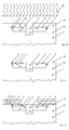
- a first mask 42 having a polycrystalline silicon layer 44 with openings for the creation of two channel layers 4, 4' is applied as shown in FIG 6 .
- first a continuous stack of layers comprising a thin oxide (SiO 2 ), polycrystalline silicon and oxide layer is formed, which is then etched down to form the first mask 42 having two openings for the channel layers 4, 4'.
- the openings have a width of up to 5 ⁇ m (width shall be the largest diameter of a circle that may be laid into a region/opening in a plane parallel to the first side 12) and a distance between the two openings up to 7 ⁇ m.
- the total mask stack shall have such a thickness that a dopant is hindered from penetration into the substrate product 10 in such areas, which are covered by the mask.
- the dopants shall penetrate into the substrate product 10 at the positions of the mask openings.
- first dopant 41 (p dopant) is applied, e.g. by implantation or deposition for the creation of the channel layers 4, 4'.
- p dopant 41 aluminum or boron is applied as first dopant 41.
- This process may be performed at an elevated temperature, exemplarily at a temperature up to 700 °C.
- All dopants 31, 41, 51, 61 are applied at any appropriate angle to the first main side 20. They may be applied perpendicular to the first main side 20, but if desired any other incident angle may be used.
- a dose between 1 * 10 11 and 1 * 10 16 cm -2 and/or an energy between 1 keV and 1 MeV may be applied.
- channel layers 4, 4' may be created having a doping concentration between 1 * 10 16 and 1 * 10 18 cm -3 .
- the first dopant 41 may be applied into a channel layer depth 40 of at maximum 2 ⁇ m.
- another oxide layer is generated as further layer (e.g. by oxidizing the polycrystalline silicon layer to form another oxide layer), which covers the remaining polycrystalline silicon layer 44 to the top and lateral sides, so that the openings are narrowed ( FIG 7 ), thereby forming a second mask 32, which is self-aligned to the first mask 42.
- the exemplarily described process may be called self-aligned process by oxidation of polycrystalline silicon.
- the total mask stack shall have such a thickness that a dopant is hindered from penetration into the substrate product 10 in such areas, which are covered by the mask.
- a second n dopant 31 is applied (implanted/deposited) for the creation of the two source regions 3, 3'.
- These source regions 3, 3' are shallower, but higher doped than the channel layers 4, 4', so that the channel layers 4, 4 'separate the source regions 3, 3' from the drift layer 2.
- the second dopant 31 is applied with a dose of exemplarily between 1 * 10 13 and 1 * 10 16 cm -2 and/or an energy between 1 keV and 500 keV up to a source region depth 30 of exemplarily at maximum 0.5 ⁇ m.
- a continuous stack of layers as described beforehand i.e. base mask layer, which may be an oxide layer, a polycrystalline silicon layer and a covering mask layer. Again, these layers are etched to form openings and a first dopant 41 is applied. Then a top mask layer 49 is applied as a continuous layer, exemplarily by deposition, which is made of a different material than the covering mask layer of the first mask, exemplary silicon nitride or polycrystalline silicon ( FIG 23 ). Afterwards, an etch step (exemplarily a dry etch) is performed without a protection mask. By this step the top mask layer 49 is removed on top of the first mask 42 and in the first mask openings.
- base mask layer which may be an oxide layer, a polycrystalline silicon layer and a covering mask layer.
- these layers are etched to form openings and a first dopant 41 is applied.
- a top mask layer 49 is applied as a continuous layer, exemplarily by deposition, which is made of a different material than the covering mask layer of the first
- the etch process stops at the covering mask layer of the first mask 42 and on the SiC substrate product 10.
- the top mask layer material or at least part of the top mask layer material remains on the lateral sides of the openings (thereby forming a remaining top mask layer 49'), such that the first mask 42 and the remaining top mask layer 49' form a second mask 32 ( FIG 24 ).
- the etch step is performed in a directional manner such that the top mask layer is sensitive to the etching (i.e. the top mask layer is removed on the top of the first mask 42 and at the bottom of the first mask openings) but such that it remains on the sidewalls of the first mask 42 and such that the covering mask layer acts as an etch stop.
- top mask layer e.g. SiN, polycrystalline silicon or SiO2
- the top mask layer e.g. SiN, polycrystalline silicon or SiO2
- This technological approach may be called self-aligned process by spacers (not shown in a figure).
- the first mask 42 and further layer are removed between the two source regions 3, 3', thereby forming a third mask 52, which has the same lateral extension as the outer limits of the openings of the second mask 32, but forms only one opening ( FIG 8 ).
- This mask 52 is again self-aligned to the first and second mask 42, 32.
- a third dopant 51 (p dopant) is applied (implanted/deposited) for the creation of the well layer 5, 5' up to the well layer depth 50.
- the third dopant 51 e.g.
- the well layer 5 is created to have a doping concentration, which is at least 10 times higher than the doping concentration of the at least one channel layer 4, 4' or, exemplarily to have a doping concentration which is between 10 times and 100 times higher than the doping concentration of the at least one channel layer 4, 4'.
- the doping concentration of the well layer 5 may be between 1 * 10 18 and 1 * 10 20 cm -3 or between 1 * 10 17 and 1 * 10 21 cm -3 .
- the well layers 5, 5' may also be formed with a retrograde profile, which means that a maximum doping concentration of the well layers 5, 5' is arranged close to the p/n junction to the drift layer 2, whereas the local doping concentration decreases towards the first main side 20.
- the doping concentrations of the layers/regions shall be understood as the maximum doping concentrations of the layers/regions if not stated otherwise.
- the implantation/deposition may be performed at a temperature higher than room temperature, exemplarily at a temperature up to 700 °C.
- the well layer depth 50 is at least as large as the channel layer depth 40. It shall be ensured that the well layer doesn't deplete during blocking conditions, thereby preventing a short between the first and second main electrode.
- the source regions 3, 3' are overcompensated layers, which means that in these layers also a dopant of the other conductivity type is present, e.g. in the source regions 3, 3' also the first dopant 41 for the channel layer 4, 4' and the third dopant 51 for the well layer 5, 5' are applied, but as the second n dopant 31 dominates, this layer is n-type (higher n-doping concentration).
- the third mask 52 is then removed after having created the source regions 3, 3', channel layers 4, 4' and well layer 5.
- a new continuous mask material layer which can be made from oxide is applied and etched to have an opening above the region between the two source regions 3, 3', thereby forming a seventh mask 62 ( FIG 10 ).
- a fourth dopant 61 (p dopant, e.g. Al or B) may be applied, e.g. with a dose between 1 * 10 11 and 1 * 10 16 cm -2 and/or an energy between 1 keV and 1 MeV up to a plug depth 60, which is at least as great as or greater than the well layer depth 50.
- the plug depth 60 is 1.05 to 1.5 times (i.e.
- An activation anneal step at a high temperature e.g. between 1500 °C to 1900 °C may follow.
- a sacrificial oxidation step may be performed. Due to the introduction of the plug 6, the well layer 5 is split into two well layers 5, 5'.
- first insulating layer 72s which cover the drift layer 2 at those parts extending to the surface at the first side 12, the channel layers 4, 4' and the outer parts of the source regions 3, 3'.
- the outer parts shall means those parts of the two source regions 3, 3' not facing each other.
- An electrically conductive gate layer 70 is applied and on top of it, a second insulating layer 74 is applied which electrically insulates the gate layer 70 from the first main electrode 9.
- a first main electrode 9 as ohmic contact in form of an emitter electrode for an IGBT 1 or a source electrode for a MOSFET 1' (metal-oxide semiconductor field-effect transistor) is created.
- the first main electrode 9 is created by first applying a metallic layer in the opening to contact the p++ plug 6, the well layers 5, 5' and the source regions 3, 3' and then another metallic layer additionally covering the second insulating layer 74 on top of the gate layer 70 is applied ( FIG 13 ).
- a second main electrode 90 as ohmic contact in form of a collector electrode for an IGBT 1 or a drain electrode for a MOSFET 1' is created.
- p channel layers 4, 4' and source regions 3, 3' are created in one MOS cell as separate regions, wherein the well layers 5, 5' are first created as one common layer ( FIG 8 ) and by the introduction of the p++ plug 6 the well layer 5, 5' is split into two separate well layers 5, 5' on the lateral sides of the plug 6. Therefore, the term well layer shall also cover two well layers 5, 5', separated from each other by the plug 6 and the term channel layer shall cover two channel layers 4, 4', separated from each other by the well layers 5, 5'.
- step (b) an alternative manufacturing method for the step (b) is shown.
- a first mask layer 35 and on top of it a second mask layer 36 is applied on the first side 12.
- the first mask layer 35 has a higher etching selectivity than the second mask layer 36, what shall mean that in the following etching process the material of the first mask layer 35 is more sensitive to the etching process than the material of the second mask layer 36. Openings are created through the first and second mask layer 35, 36 down to the substrate product 10 (i.e. to the drift layer 2), thereby creating a fourth mask 34 on the first side 12 ( FIG 14 ).
- a second dopant 31 (n dopant) is applied for the creation of the two source regions 3, 3' up to the source region depth 30.
- All values for the source regions 3, 3', channel layers 4, 4', the well layer 5, 5', and the plug 6 like dose, energy, doping concentrations, dopant type etc. shall have the same exemplary ranges as afore disclosed in the sections about the manufacturing process.
- the total mask stack shall have such a thickness that a dopant is hindered from penetration into the substrate product 10 in such areas, which are covered by the mask.
- the dopants shall penetrate into the substrate product 10 at the positions of the mask openings.
- a third dopant 51 (p dopant) is applied for the creation of the well layer 5 up to the well layer depth 50.
- an etching step is performed on the first side 12, by which etching the first mask layer 35 is farther removed at the openings than the second mask layer 36 due to the higher etching selectivity of the first mask layer 35 so that the openings are enlarged in a self-aligned manner.
- the second mask layer 36 may now be removed, thereby creating a sixth mask 46 formed by the remaining first mask layer 35'.
- a first dopant 41 p dopant
- p channel layers 4, 4' and source regions 3, 3' are created in one MOS cell as separate regions (source regions 3, 3' as separate regions by masking and channel layers 4, 4' by the region being dominated in the central area by the higher doping concentration of the well layer 5, 5', wherein the well layers 5, 5' are first created as one common layer 5 ( FIG 8 ) and by the introduction of the p++ plug 6 the well layer 5 is split into two separate well layers 5, 5' on the lateral sides of the plug 6.
- step (b) a retrograde p doped layer as a common channel and well layer (4, 4', 5, 5') is created and source regions 3, 3' are created before or after the retrograde layer (4, 4', 5, 5').
- the retrograde layer (4, 4', 5, 5') has such doping concentration that on the outer lateral sides of the source regions 3, 3' the retrograde layer has a low doping concentration (i.e. channel layers 4, 4') up to the source region depth 30, which then rises to greater depths to a high doping concentration below the source regions 3, 3' (i.e. well layers 5, 5').
- the common retrograde layer is split into a retrograde layer 4, 5 and 4', 5'.
- the plug 6 may also be created as a retrograde layer having a lower doping concentration in shallow depth and a higher up to a maximum doping concentration in greater depth, which depth may exemplarily be located as deep as the depth of the maximum doping concentration of the well layers 5, 5' or deeper.
- inventive structure and manufacturing method having a deep p++ plug may be applied to different semiconductor devices having MOS cell structures such as MOSFETs and MOS controlled IGBTs.
- the conductivity types of the layers are switched, i.e. all layers of the first conductivity type are p type (e.g. the drift layer 2 and the source regions 3) and all layers of the second conductivity type are n type (e.g. channel layer 4, the well layer 5 and the plug 6).
Priority Applications (11)
| Application Number | Priority Date | Filing Date | Title |
|---|---|---|---|
| EP15197558.8A EP3176812A1 (de) | 2015-12-02 | 2015-12-02 | Halbleiterbauelement und verfahren zur herstellung solch eines halbleiterbauelements |
| PCT/EP2016/076085 WO2017092940A1 (en) | 2015-12-02 | 2016-10-28 | Semiconductor device and method for manufacturing such a semiconductor device |
| JP2018528766A JP6807390B2 (ja) | 2015-12-02 | 2016-10-28 | 半導体装置およびその製造方法 |
| EP16788686.0A EP3384523B1 (de) | 2015-12-02 | 2016-10-28 | Halbleiterbauelement und verfahren zur herstellung eines solchen halbleiterbauelements |
| EP16787897.4A EP3384522B1 (de) | 2015-12-02 | 2016-10-28 | Halbleiterbauelement und verfahren zur herstellung eines solchen halbleiterbauelements |
| CN201680080911.7A CN108604551B (zh) | 2015-12-02 | 2016-10-28 | 半导体装置以及用于制造这种半导体装置的方法 |
| CN201680080912.1A CN108604552B (zh) | 2015-12-02 | 2016-10-28 | 半导体装置以及用于制造这种半导体装置的方法 |
| JP2018528801A JP7432071B2 (ja) | 2015-12-02 | 2016-10-28 | 半導体装置およびその製造方法 |
| PCT/EP2016/076084 WO2017092939A1 (en) | 2015-12-02 | 2016-10-28 | Semiconductor device and method for manufacturing such a semiconductor device |
| US15/997,298 US10361082B2 (en) | 2015-12-02 | 2018-06-04 | Semiconductor device and method for manufacturing such a semiconductor device |
| US15/996,589 US10553437B2 (en) | 2015-12-02 | 2018-06-04 | Semiconductor device and method for manufacturing such a semiconductor device |
Applications Claiming Priority (1)
| Application Number | Priority Date | Filing Date | Title |
|---|---|---|---|
| EP15197558.8A EP3176812A1 (de) | 2015-12-02 | 2015-12-02 | Halbleiterbauelement und verfahren zur herstellung solch eines halbleiterbauelements |
Publications (1)
| Publication Number | Publication Date |
|---|---|
| EP3176812A1 true EP3176812A1 (de) | 2017-06-07 |
Family
ID=54771016
Family Applications (3)
| Application Number | Title | Priority Date | Filing Date |
|---|---|---|---|
| EP15197558.8A Withdrawn EP3176812A1 (de) | 2015-12-02 | 2015-12-02 | Halbleiterbauelement und verfahren zur herstellung solch eines halbleiterbauelements |
| EP16788686.0A Active EP3384523B1 (de) | 2015-12-02 | 2016-10-28 | Halbleiterbauelement und verfahren zur herstellung eines solchen halbleiterbauelements |
| EP16787897.4A Active EP3384522B1 (de) | 2015-12-02 | 2016-10-28 | Halbleiterbauelement und verfahren zur herstellung eines solchen halbleiterbauelements |
Family Applications After (2)
| Application Number | Title | Priority Date | Filing Date |
|---|---|---|---|
| EP16788686.0A Active EP3384523B1 (de) | 2015-12-02 | 2016-10-28 | Halbleiterbauelement und verfahren zur herstellung eines solchen halbleiterbauelements |
| EP16787897.4A Active EP3384522B1 (de) | 2015-12-02 | 2016-10-28 | Halbleiterbauelement und verfahren zur herstellung eines solchen halbleiterbauelements |
Country Status (5)
| Country | Link |
|---|---|
| US (2) | US10553437B2 (de) |
| EP (3) | EP3176812A1 (de) |
| JP (2) | JP7432071B2 (de) |
| CN (2) | CN108604552B (de) |
| WO (2) | WO2017092940A1 (de) |
Families Citing this family (6)
| Publication number | Priority date | Publication date | Assignee | Title |
|---|---|---|---|---|
| EP3176812A1 (de) * | 2015-12-02 | 2017-06-07 | ABB Schweiz AG | Halbleiterbauelement und verfahren zur herstellung solch eines halbleiterbauelements |
| CN109148590A (zh) * | 2018-08-30 | 2019-01-04 | 全球能源互联网研究院有限公司 | 半导体器件及其制备方法 |
| US10985242B2 (en) * | 2019-03-06 | 2021-04-20 | Littelfuse, Inc. | Power semiconductor device having guard ring structure, and method of formation |
| JP2021002624A (ja) * | 2019-06-24 | 2021-01-07 | 株式会社デンソー | 窒化物半導体装置 |
| CN112038234B (zh) * | 2020-08-13 | 2022-11-22 | 杭州芯迈半导体技术有限公司 | SiC MOSFET器件及其制造方法 |
| CN117133800B (zh) * | 2023-10-25 | 2024-03-26 | 合肥海图微电子有限公司 | 一种绝缘栅双极型晶体管及其制作方法 |
Citations (9)
| Publication number | Priority date | Publication date | Assignee | Title |
|---|---|---|---|---|
| US4914047A (en) * | 1987-03-03 | 1990-04-03 | Fuji Electric Co., Ltd. | Method of producing insulated gate MOSFET employing polysilicon mask |
| US7074643B2 (en) | 2003-04-24 | 2006-07-11 | Cree, Inc. | Silicon carbide power devices with self-aligned source and well regions and methods of fabricating same |
| US7517807B1 (en) * | 2006-07-26 | 2009-04-14 | General Electric Company | Methods for fabricating semiconductor structures |
| US20100200931A1 (en) * | 2009-02-10 | 2010-08-12 | General Electric Company | Mosfet devices and methods of making |
| JP2010267762A (ja) * | 2009-05-14 | 2010-11-25 | Mitsubishi Electric Corp | 半導体装置およびその製造方法 |
| JP2011049267A (ja) * | 2009-08-26 | 2011-03-10 | Mitsubishi Electric Corp | 半導体装置及びその製造方法 |
| US8212283B2 (en) | 2009-04-29 | 2012-07-03 | Abb Technology Ag | Reverse-conducting semiconductor device |
| US20120205670A1 (en) * | 2009-10-23 | 2012-08-16 | Panasonic Corporation | Semiconductor device and process for production thereof |
| WO2015042146A1 (en) * | 2013-09-20 | 2015-03-26 | Cree, Inc. | Vertical field-effect transistor device having a bypass diode |
Family Cites Families (16)
| Publication number | Priority date | Publication date | Assignee | Title |
|---|---|---|---|---|
| JPH0724317B2 (ja) * | 1988-07-28 | 1995-03-15 | 三菱電機株式会社 | 半導体レーザの製造方法 |
| DE19832329A1 (de) * | 1997-07-31 | 1999-02-04 | Siemens Ag | Verfahren zur Strukturierung von Halbleitern mit hoher Präzision, guter Homogenität und Reproduzierbarkeit |
| DE10137676B4 (de) * | 2001-08-01 | 2007-08-23 | Infineon Technologies Ag | ZVS-Brückenschaltung zum entlasteten Schalten |
| JP4635470B2 (ja) * | 2004-04-19 | 2011-02-23 | 株式会社デンソー | 炭化珪素半導体装置およびその製造方法 |
| US7118970B2 (en) * | 2004-06-22 | 2006-10-10 | Cree, Inc. | Methods of fabricating silicon carbide devices with hybrid well regions |
| JP4627272B2 (ja) * | 2006-03-09 | 2011-02-09 | 三菱電機株式会社 | 炭化珪素半導体装置および炭化珪素半導体装置の製造方法 |
| JP2008147576A (ja) * | 2006-12-13 | 2008-06-26 | Sumitomo Electric Ind Ltd | 半導体装置の製造方法 |
| KR100841337B1 (ko) * | 2007-01-12 | 2008-06-26 | 삼성전자주식회사 | 반도체 소자 및 그 형성 방법 |
| JP5428144B2 (ja) * | 2007-10-01 | 2014-02-26 | 富士電機株式会社 | 半導体装置 |
| JP5332175B2 (ja) * | 2007-10-24 | 2013-11-06 | 富士電機株式会社 | 制御回路を備える半導体装置 |
| JP4917582B2 (ja) * | 2008-07-25 | 2012-04-18 | 住友化学株式会社 | アクティブマトリクス基板、ディスプレイパネル、表示装置およびアクティブマトリクス基板の製造方法 |
| US8563986B2 (en) * | 2009-11-03 | 2013-10-22 | Cree, Inc. | Power semiconductor devices having selectively doped JFET regions and related methods of forming such devices |
| WO2012165329A1 (ja) * | 2011-05-27 | 2012-12-06 | 新電元工業株式会社 | トレンチゲートパワー半導体装置及びその製造方法 |
| KR101603567B1 (ko) * | 2011-09-21 | 2016-03-15 | 미쓰비시덴키 가부시키가이샤 | 탄화 규소 반도체장치 및 그 제조방법 |
| JP6256148B2 (ja) * | 2014-03-27 | 2018-01-10 | 住友電気工業株式会社 | 炭化珪素半導体装置およびその製造方法 |
| EP3176812A1 (de) * | 2015-12-02 | 2017-06-07 | ABB Schweiz AG | Halbleiterbauelement und verfahren zur herstellung solch eines halbleiterbauelements |
-
2015
- 2015-12-02 EP EP15197558.8A patent/EP3176812A1/de not_active Withdrawn
-
2016
- 2016-10-28 WO PCT/EP2016/076085 patent/WO2017092940A1/en active Application Filing
- 2016-10-28 CN CN201680080912.1A patent/CN108604552B/zh active Active
- 2016-10-28 JP JP2018528801A patent/JP7432071B2/ja active Active
- 2016-10-28 EP EP16788686.0A patent/EP3384523B1/de active Active
- 2016-10-28 JP JP2018528766A patent/JP6807390B2/ja active Active
- 2016-10-28 EP EP16787897.4A patent/EP3384522B1/de active Active
- 2016-10-28 CN CN201680080911.7A patent/CN108604551B/zh active Active
- 2016-10-28 WO PCT/EP2016/076084 patent/WO2017092939A1/en active Application Filing
-
2018
- 2018-06-04 US US15/996,589 patent/US10553437B2/en active Active
- 2018-06-04 US US15/997,298 patent/US10361082B2/en active Active
Patent Citations (9)
| Publication number | Priority date | Publication date | Assignee | Title |
|---|---|---|---|---|
| US4914047A (en) * | 1987-03-03 | 1990-04-03 | Fuji Electric Co., Ltd. | Method of producing insulated gate MOSFET employing polysilicon mask |
| US7074643B2 (en) | 2003-04-24 | 2006-07-11 | Cree, Inc. | Silicon carbide power devices with self-aligned source and well regions and methods of fabricating same |
| US7517807B1 (en) * | 2006-07-26 | 2009-04-14 | General Electric Company | Methods for fabricating semiconductor structures |
| US20100200931A1 (en) * | 2009-02-10 | 2010-08-12 | General Electric Company | Mosfet devices and methods of making |
| US8212283B2 (en) | 2009-04-29 | 2012-07-03 | Abb Technology Ag | Reverse-conducting semiconductor device |
| JP2010267762A (ja) * | 2009-05-14 | 2010-11-25 | Mitsubishi Electric Corp | 半導体装置およびその製造方法 |
| JP2011049267A (ja) * | 2009-08-26 | 2011-03-10 | Mitsubishi Electric Corp | 半導体装置及びその製造方法 |
| US20120205670A1 (en) * | 2009-10-23 | 2012-08-16 | Panasonic Corporation | Semiconductor device and process for production thereof |
| WO2015042146A1 (en) * | 2013-09-20 | 2015-03-26 | Cree, Inc. | Vertical field-effect transistor device having a bypass diode |
Also Published As
| Publication number | Publication date |
|---|---|
| WO2017092940A1 (en) | 2017-06-08 |
| US20180350602A1 (en) | 2018-12-06 |
| EP3384522B1 (de) | 2019-07-17 |
| CN108604552A (zh) | 2018-09-28 |
| JP2018537858A (ja) | 2018-12-20 |
| JP6807390B2 (ja) | 2021-01-06 |
| JP2018537859A (ja) | 2018-12-20 |
| CN108604552B (zh) | 2022-03-22 |
| CN108604551A (zh) | 2018-09-28 |
| US10553437B2 (en) | 2020-02-04 |
| WO2017092939A1 (en) | 2017-06-08 |
| EP3384523A1 (de) | 2018-10-10 |
| JP7432071B2 (ja) | 2024-02-16 |
| EP3384523B1 (de) | 2019-07-17 |
| EP3384522A1 (de) | 2018-10-10 |
| US20180286963A1 (en) | 2018-10-04 |
| CN108604551B (zh) | 2022-09-06 |
| US10361082B2 (en) | 2019-07-23 |
Similar Documents
| Publication | Publication Date | Title |
|---|---|---|
| US10361082B2 (en) | Semiconductor device and method for manufacturing such a semiconductor device | |
| US10516022B2 (en) | Method for manufacturing a semiconductor device | |
| US8659076B2 (en) | Semiconductor device structures and related processes | |
| CN109473477B (zh) | 半导体装置 | |
| EP3479410B1 (de) | Graben-leistungs-mosfet mit kurzem kanal | |
| US9525043B2 (en) | Semiconductor device and method of manufacturing a semiconductor device | |
| US20190035928A1 (en) | Short channel trench power mosfet | |
| US20210043735A1 (en) | Short channel trench power mosfet and method | |
| EP3223316A1 (de) | Leistungshalbleiterbauelement mit breiter bandbreite und verfahren zur herstellung solch eines bauelements |
Legal Events
| Date | Code | Title | Description |
|---|---|---|---|
| AK | Designated contracting states |
Kind code of ref document: A1 Designated state(s): AL AT BE BG CH CY CZ DE DK EE ES FI FR GB GR HR HU IE IS IT LI LT LU LV MC MK MT NL NO PL PT RO RS SE SI SK SM TR |
|
| AX | Request for extension of the european patent |
Extension state: BA ME |
|
| PUAI | Public reference made under article 153(3) epc to a published international application that has entered the european phase |
Free format text: ORIGINAL CODE: 0009012 |
|
| STAA | Information on the status of an ep patent application or granted ep patent |
Free format text: STATUS: THE APPLICATION IS DEEMED TO BE WITHDRAWN |
|
| 18D | Application deemed to be withdrawn |
Effective date: 20171208 |