EP3158571B1 - Dispositif de coupure pour interrompre un courant continu - Google Patents
Dispositif de coupure pour interrompre un courant continu Download PDFInfo
- Publication number
- EP3158571B1 EP3158571B1 EP15714411.4A EP15714411A EP3158571B1 EP 3158571 B1 EP3158571 B1 EP 3158571B1 EP 15714411 A EP15714411 A EP 15714411A EP 3158571 B1 EP3158571 B1 EP 3158571B1
- Authority
- EP
- European Patent Office
- Prior art keywords
- circuit breaker
- current
- arc
- arrangement
- switching
- Prior art date
- Legal status (The legal status is an assumption and is not a legal conclusion. Google has not performed a legal analysis and makes no representation as to the accuracy of the status listed.)
- Active
Links
- 239000004065 semiconductor Substances 0.000 claims description 72
- 238000001514 detection method Methods 0.000 claims description 4
- 238000002955 isolation Methods 0.000 claims description 2
- 230000001681 protective effect Effects 0.000 description 9
- 239000003990 capacitor Substances 0.000 description 7
- 238000010586 diagram Methods 0.000 description 4
- 230000001960 triggered effect Effects 0.000 description 4
- 230000000903 blocking effect Effects 0.000 description 2
- 238000000926 separation method Methods 0.000 description 2
- 230000004913 activation Effects 0.000 description 1
- 238000013459 approach Methods 0.000 description 1
- 238000001816 cooling Methods 0.000 description 1
- 230000001419 dependent effect Effects 0.000 description 1
- 230000000694 effects Effects 0.000 description 1
- 230000005611 electricity Effects 0.000 description 1
- 238000004146 energy storage Methods 0.000 description 1
- 230000003628 erosive effect Effects 0.000 description 1
- 238000009434 installation Methods 0.000 description 1
- 238000000034 method Methods 0.000 description 1
Images


Classifications
-
- H—ELECTRICITY
- H02—GENERATION; CONVERSION OR DISTRIBUTION OF ELECTRIC POWER
- H02H—EMERGENCY PROTECTIVE CIRCUIT ARRANGEMENTS
- H02H3/00—Emergency protective circuit arrangements for automatic disconnection directly responsive to an undesired change from normal electric working condition with or without subsequent reconnection ; integrated protection
- H02H3/08—Emergency protective circuit arrangements for automatic disconnection directly responsive to an undesired change from normal electric working condition with or without subsequent reconnection ; integrated protection responsive to excess current
- H02H3/087—Emergency protective circuit arrangements for automatic disconnection directly responsive to an undesired change from normal electric working condition with or without subsequent reconnection ; integrated protection responsive to excess current for dc applications
-
- H—ELECTRICITY
- H01—ELECTRIC ELEMENTS
- H01H—ELECTRIC SWITCHES; RELAYS; SELECTORS; EMERGENCY PROTECTIVE DEVICES
- H01H9/00—Details of switching devices, not covered by groups H01H1/00 - H01H7/00
- H01H9/54—Circuit arrangements not adapted to a particular application of the switching device and for which no provision exists elsewhere
- H01H9/541—Contacts shunted by semiconductor devices
- H01H9/542—Contacts shunted by static switch means
-
- H—ELECTRICITY
- H01—ELECTRIC ELEMENTS
- H01H—ELECTRIC SWITCHES; RELAYS; SELECTORS; EMERGENCY PROTECTIVE DEVICES
- H01H71/00—Details of the protective switches or relays covered by groups H01H73/00 - H01H83/00
- H01H71/10—Operating or release mechanisms
- H01H71/12—Automatic release mechanisms with or without manual release
- H01H71/123—Automatic release mechanisms with or without manual release using a solid-state trip unit
- H01H2071/124—Automatic release mechanisms with or without manual release using a solid-state trip unit with a hybrid structure, the solid state trip device being combined with a thermal or a electromagnetic trip
-
- H—ELECTRICITY
- H01—ELECTRIC ELEMENTS
- H01H—ELECTRIC SWITCHES; RELAYS; SELECTORS; EMERGENCY PROTECTIVE DEVICES
- H01H71/00—Details of the protective switches or relays covered by groups H01H73/00 - H01H83/00
- H01H71/10—Operating or release mechanisms
- H01H71/1009—Interconnected mechanisms
-
- H—ELECTRICITY
- H01—ELECTRIC ELEMENTS
- H01H—ELECTRIC SWITCHES; RELAYS; SELECTORS; EMERGENCY PROTECTIVE DEVICES
- H01H9/00—Details of switching devices, not covered by groups H01H1/00 - H01H7/00
- H01H9/54—Circuit arrangements not adapted to a particular application of the switching device and for which no provision exists elsewhere
- H01H9/548—Electromechanical and static switch connected in series
Definitions
- the invention relates to a disconnecting device for direct current interruption between a direct current source and an electrical supply or a load according to the preamble of claim 1.
- a disconnecting device is known from US Pat WO 2010/108565 A1 and from their priority DE 20 2009 004 198 U1 known.
- Direct current (DC) is understood to mean a nominal current range between 4A DC and 250A DC with a direct voltage range between 300V DC and 1500V DC .
- a direct voltage source for example a photovoltaic system
- an operating current and an operating voltage in the range between 180V (DC) and 1500V (DC) and on the other hand - for example for installation, assembly or service purposes and for general personal protection - a reliable separation of the electrical components, equipment and/or a load from the direct current source
- an appropriate disconnecting device must be able to carry out an interruption under load, i.e. without first switching off the direct current source.
- a mechanical switch can be used to disconnect the load, with the advantage that when the contact opens, the electrical device (inverter) is electrically isolated from the direct current source (photovoltaic system).
- the disadvantage is that such mechanical switching contacts are worn out very quickly due to the arc that occurs when the contact opens, or additional effort is required to enclose and cool the arc, which is usually done by a corresponding mechanical switch with an arcing chamber.
- the semiconductor electronics have an energy storage device, which is charged as a result of the arc within the duration of the arc and by means of which the semiconductor electronics are operated. Due to the current conductivity of the semiconductor circuit in the event of an arc, a comparatively low-impedance current path is connected in parallel with this, which leads to the arc being extinguished comparatively early and thus to a comparatively low load on the isolating device or interruption unit.
- a switching device with a low-voltage switch arranged in a main current path, which in series contains at least one tripping element that scans the current to be switched off and a main switching point, as well as an auxiliary current path connected in parallel to the main switching point.
- a controllable semiconductor switch and a load-reducing element are arranged in parallel with one another.
- a control device for the semiconductor switch is located parallel to the main switching point.
- the auxiliary current path contains an auxiliary switching point which is connected in series with the parallel connection of the controllable semiconductor switch and the load-reducing element and which opens with a time delay after the opening of the semiconductor switch when it is switched off.
- the invention is based on the object of specifying a particularly suitable disconnecting device for direct current interruption between a direct current source and an electrical device or load.
- the separating device also referred to below as a hybrid circuit breaker, comprises a circuit breaker arrangement having at least one first current-carrying circuit breaker with a magnetic release and semiconductor electronics connected in parallel with the first circuit breaker of the circuit breaker arrangement Essentially comprises at least one semiconductor switch, preferably an IGBT.
- a circuit breaker with a magnetic trigger is understood to mean one with a purely magnetic, thermal-magnetic or hydraulic-mechanical trigger and thus generally a magnetic, thermal-magnetic or hydraulic-mechanical circuit breaker.
- the semiconductor electronics are provided and set up to be current-blocking when the circuit breaker is live and to be current-conducting at least briefly when the circuit breaker is triggered as a result of an overcurrent and/or a switching signal. H. an arc current generated as a result of an arc commutates from the circuit breaker to the semiconductor electronics.
- the semiconductor electronics of the isolating switch according to the invention preferably has no additional energy source and is therefore current-blocking when the mechanical switch is closed, ie has a high resistance and is therefore practically without current and voltage. Since no current flows through the semiconductor electronics when the mechanical switching contacts of the or each protective switch of the protective switch arrangement are closed and therefore no voltage drop occurs in particular across the or each semiconductor switch, the semiconductor circuit also does not generate any power losses when the switching contacts of the protective switch arrangement are closed. Rather, the semiconductor electronics gains the energy required for their operation from the separating device itself Opening the switch contacts of the or each circuit breaker of the circuit breaker arrangement resulting arc used.
- a control input of the semiconductor electronics or the semiconductor switch is suitably connected to the or each circuit breaker in such a way that when the switch contacts of the circuit breaker arrangement open, the arc voltage makes the parallel semiconductor electronics conductive, ie low-impedance and thus conductive.
- the circuit breaker arrangement of the isolating device has at least one second circuit breaker, which or whose switching contacts are connected in series, and the at least one first circuit breaker of the circuit breaker arrangement is connected in series with the semiconductor electronics, if the circuit breaker arrangement trips, the load is electrically isolated from the direct current source and thus a complete galvanic DC interruption is achieved by opening this hybrid circuit breaker.
- the separating device has a module (arc fault module) for arc detection and/or for arc detection.
- This module interacts with a current sensor for detecting the current flowing through the or each circuit breaker, ie it is electrically connected to the current sensor.
- the module evaluates the recorded current with regard to its time course and/or its rate of rise (dl/dt). If a specific characteristic of the detected current is detected, for example if an arc is inferred, the module transmits a tripping signal to the or each circuit breaker to trip it.
- the module is preferably connected to a motor or magnetic drive, which in turn is coupled to the or each circuit breaker or to its/their switching mechanism for separating the circuit breaker contacts.
- the separator can be two-pole or four-pole.
- at least one circuit breaker in the circuit breaker arrangement preferably a series connection of at least two circuit breakers with circuit breaker isolating contacts, connected in a main current path (positive current path) of the isolating device. Additionally or alternatively, at least one circuit breaker or circuit breaker isolating contact of the circuit breaker arrangement is connected into the return current path (negative current path) of the disconnecting device.
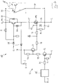
- FIG. 1 shows a schematic of a disconnecting device 1 which, in the exemplary embodiment, is connected between a direct voltage source 2 for generating a direct voltage U DC and a direct current I N and a load 3 .
- the separating device 1 comprises a circuit breaker arrangement in the form of a series connection of two magnetic, in particular hydraulic-magnetic, circuit breakers 5, 6, whose switching contacts coupled to a switching mechanism 7 are designated C 1 and C 2 .
- Another circuit breaker 8 or switching contact C 3 is in the reverse current or negative path (Return line) 9 of the separating device 1 is connected and also coupled to the switching mechanism 7 .
- Semiconductor electronics 10 are connected in parallel with one of the circuit breakers 5 , 6, 8, here the circuit breaker 5 or its switching contact C1.
- the circuit breakers 5, 6, 8 and the semiconductor electronics 10 form a self-sufficient hybrid circuit breaker as a separator 1 for nominal DC currents (direct currents) I N between 4A DC and 25oA DC at a direct voltage U DC between 300V DC and 1500V DC .
- the semiconductor electronics 10 essentially comprises at least one semiconductor switch 10a, 10b, which is connected in parallel to the protective switch 5 of the protective switch arrangement 5, 6, 8.
- the gate of an IGBT preferably used as a semiconductor switch 10b forms the control input or a control connection 11 of the semiconductor circuit 10. This control input or control connection 11 can be routed to the main current path 4 via a drive circuit.
- FIG 1 shows a four-pole disconnecting device 1 or a four-pole hybrid circuit breaker with supply-side inputs or input terminals E 1 and E 2 and load-side outputs or output terminals A 1 and A 2
- figure 2 a two-pole separator 1 or a two-pole hybrid circuit breaker is shown.
- the respective circuit breakers 5, 6, 8 or their switching contacts C 1 , C 2 , C 3 can each have a switching mechanism 7 and a magnetic or magnetic-hydraulic release 12 .
- the circuit breakers 5, 6, 8 are suitably assigned a common switching mechanism 7 and a common trigger (triggering device) 12.
- the switching contacts C n of the other circuit breakers are then preferably mechanically coupled to the switching mechanism 7 of the main circuit breaker, here the circuit breaker 5, in order to ensure at least approximately simultaneous tripping of the circuit breakers 5, 6, 8 and contact separation of the switching contacts C n of all circuit breakers 5, 6, 8 to effect the circuit breaker arrangement.
- the circuit breakers 5, 6, 8 or their switching contacts C n are assigned a drive 13 designed as a motor or magnet system. This is supplied with a control signal S A for circuit breaker tripping by a module 14, referred to below as the arc fault module, for arc detection or for detecting an overcurrent.
- the module 14 is connected to a current sensor 15 which detects the current I preferably flowing in the main current path 4 . The detected current I is evaluated by the module 14 .
- the Module 14 that Control or trigger signal S A generated.
- the circuit breakers 5, 6, 8 of the circuit breaker arrangement are triggered practically at the same time.
- An arc occurring in the course of the opening of their switching contacts C n causes a corresponding arcing voltage and a corresponding arcing current, which switches the previously current-blocking semiconductor electronics 10 conductive, so that the current flowing in the main current path 4 commutes to the semiconductor electronics 10 and is taken over by it until the arc is extinguished becomes.
- the semiconductor electronics 10 accepts switching currents up to a value of approximately 1000A within a very short period of time, the commutation being dependent on the circuit inductance within a corresponding time range of 50 ⁇ s to 300 ⁇ s. In the case of higher switching currents, the circuit breaker arrangement 5, 6, 8 alone takes over the shutdown and current limitation.
- a first semiconductor switch (IGBT) 10a can be seen connected in series in a cascode arrangement with a second semiconductor switch 10b in the form of a MOSFET.
- the cascode arrangement with the two semiconductor switches 10a, 10b thus forms analogously to 1 the commutation path 16 parallel to the protective switch 5 of the protective switch arrangement 5, 6, 8 and thus to the main current path 4.
- the first semiconductor switch 10a is routed between the direct current source 2 and the protective switch arrangement and there parallel to the switching contact C1 to the main current path 4.
- the potential U+ is always greater than the potential U ⁇ on the opposite side of the switch , on which the second semiconductor switch (MOSFET) 10b is connected to the main circuit 4 .
- the plus potential U+ is 0V when the switching contacts C n of the circuit breaker arrangement 5, 6, 8 are closed.
- the first semiconductor switch (IGBT) 10a is connected to a freewheeling diode D2.
- a first Zener diode D3 is connected to the potential U - on the anode side and to the gate (control input 11) of the first semiconductor switch (IGBT) 10a on the cathode side tied together.
- Another Zener diode D4 is connected to the control input 11 on the cathode side and to the emitter of the first semiconductor switch (IGBT) 10a on the anode side.
- a diode D1 is connected to a center or cascode tap 17 between the first and second semiconductor switches 10a and 10b of the cascode arrangement on the anode side, which is connected to the potential U ⁇ on the cathode side via a capacitor C serving as an energy store.
- a transistor T1 connected to ohmic resistors R1 and R2 is connected via further resistors R3 and R4 to the gate of the second semiconductor switch 10b, which in turn is connected to the control input 12 of the semiconductor electronics 10 tied together.
- Another Zener diode D5 with a parallel resistor R5 is connected to the gate on the cathode side and to the emitter of the second semiconductor switch 10b on the anode side.
- the transistor T1 On the base side, the transistor T1 is driven via a transistor T2, which in turn is connected on the base side via an ohmic resistor R6 to a timing element 19, which is designed as a monoflop, for example.
- the transistor T2 is also connected to a further resistor R7 on the base-emitter side.
- the commutation of the switch current I which essentially corresponds to the arc current, already begins from the main current path 4 to the commutation path 16 of the semiconductor electronics 10.
- the energy store C is charged during this arcing time interval.
- the duration is set such that on the one hand sufficient energy is available for reliable activation of the semiconductor electronics 10, in particular for switching it off during a specific period of time following the period of time representing the duration of the arc.
- the period is sufficiently short, so that an undesirable contact erosion or -wear of the switching contacts C n of the circuit breaker arrangement 5, 6, 8 is avoided.
- the first semiconductor switch 10a is controlled at least to the extent via the resistor R that a sufficient charging voltage and a sufficient arc or charging current for the capacitors C is available.
- U AB 12V (DC)
- the tap voltage is used to supply the control circuit of the electronics 10, which is essentially formed by the transistors T1 and T2 as well as the timer 19 and the energy store C.
- the diode D1 which is connected to the cascode tap 17 on the anode side and to the capacitor C on the cathode side, prevents the charging current from flowing back out of the Capacitors C and the commutation path 16 in the direction of the potential U - .
- the charging capacity and thus the storage energy contained in the capacitor C is dimensioned in such a way that the semiconductor electronics 10 carry the switch current I for a period of time specified by the timer 19 .
- This time period can be set to 3 ms, for example.
- the dimensioning of this period of time and thus the setting of the timer 19 are based essentially on the application-specific or typical periods of time for complete extinguishing of the arc and after sufficient cooling of the plasma formed in the process.
- the essential requirement here is that after the electronics 10 have been switched off, with the commutation path 16 then again having a high resistance and the semiconductor electronics 10 consequently blocking the current, no new arc can occur on the circuit breaker arrangement 5, 6, 8 which has still been triggered.
- the positive potential U+ thus goes towards this operating voltage when the commutation path 16 has a high resistance as a result of the blocking of the semiconductor switches 10 and the electronics 10 thus block the current again.
- an electrical device such. B. be provided an inverter of a photovoltaic system.
Landscapes
- Driving Mechanisms And Operating Circuits Of Arc-Extinguishing High-Tension Switches (AREA)
- Emergency Protection Circuit Devices (AREA)
- Keying Circuit Devices (AREA)
Claims (6)
- Dispositif de déconnexion (1) pour l'interruption du courant continu entre une source de courant continu (UDC) et une charge (3), comprenant- un arrangement de disjoncteurs avec un premier disjoncteur (5) et avec au moins un deuxième disjoncteur (6, 8), qui est connecté en série avec le premier disjoncteur (5), et- une électronique à semi-conducteur (10) connectée en parallèle avec le premier disjoncteur (5), laquelle électronique à semi-conducteur (10) bloque le courant lorsque l'arrangement de disjoncteurs conduit le courant et qui conduit le courant au moins brièvement lorsque l'arrangement de disjoncteurs se déclenche, en ce que, lorsque l'arrangement de disjoncteurs se déclenche, un courant d'arc électrique généré à la suite d'un arc électrique commute du premier disjoncteur (5) sur l'électronique à semi-conducteur (10),- le deuxième disjoncteur (6, 8) du dispositif de protection étant connecté en série avec l'électronique à semi-conducteur (10) dans le but d'une séparation galvanique de la charge (3) de la source de courant continu (UDC) en cas de déclenchement,
caractérisé en ce- qu'au moins le premier disjoncteur (5) comprend un déclencheur magnétique (12),- que le premier disjoncteur (5) et le ou chaque deuxième disjoncteur (6, 8) ou respectivement leurs contacts de commutation (C1 , C2 , C3) sont couplés au moyen d'un verrou de connexion (7), et- qu'un entraînement (13) est couplé au ou à chaque disjoncteur (5, 6, 8) de l'arrangement de disjoncteurs pour déclencher chaque disjoncteur (5, 6, 8) dans le cas d'une surintensité détectée, en particulier lors de l'apparition de l'arc électrique. - Dispositif de déconnexion (1) selon la revendication 1,
caractérisé en ce
que l'électronique (10) à semi-conducteur a au moins un commutateur (10a, 10b) à semi-conducteur pouvant être commandé. - Dispositif de déconnexion (1) selon la revendication 1 ou 2,
caractérisé en ce
qu'une entrée de commande (11) de l'électronique à semi-conducteur (10) est connectée au premier disjoncteur (5) du dispositif de protection de telle sorte que, lorsque le disjoncteur (5) ou le contact de commutation (C1) s'ouvre, une tension d'arc électrique générée par suite d'un arc électrique au-dessus du disjoncteur (5) ou respectivement par l'intermédiaire de son contact de commutation (C1) commute l'électronique à semi-conducteur (10) de manière à conduire le courant. - Dispositif de déconnexion (1) selon l'une des revendications 1 à 3,
caractérisé en ce
qu'il est prévu un module (14) coopérant avec un capteur de courant (15) pour détecter le courant (I) passant par le ou chaque disjoncteur (5, 6, 8) de l'arrangement de disjoncteurs, pour détecter un arc électrique et/ou reconnaître un arc électrique ou pour détecter une surintensité. - Dispositif de déconnexion (1) quadripolaire selon l'une des revendications 1 à 4, comprenant- une première borne d'entrée (E1) et une première borne de sortie (A1),- une deuxième borne d'entrée (E2) et une deuxième borne de sortie (A2),- un trajet de courant principal (4) entre la première borne d'entrée (E1) et la première borne de sortie (A1), l'arrangement de disjoncteurs étant connecté dans le trajet de courant principal (4) avec le premier disjoncteur (5) avec des premiers contacts de commutation (C1) et avec le deuxième disjoncteur (6) avec des deuxièmes contacts de commutation (C2), et- un trajet de courant de retour (9) entre la deuxième borne d'entrée (E2) et la deuxième borne de sortie (A2), un troisième disjoncteur (8) avec des troisièmes contacts de commutation (C3) étant connecté dans le trajet de courant de retour (9).
- Dispositif de déconnexion (1) selon la revendication 5,
caractérisé en ce
que les contacts de commutation (C1 , C2 , C3) de l'arrangement de disjoncteurs (5, 6, 8) sont couplés au moyen d'un verrou de connexion (7) commun.
Priority Applications (1)
| Application Number | Priority Date | Filing Date | Title |
|---|---|---|---|
| EP20207521.4A EP3855465B1 (fr) | 2014-06-18 | 2015-03-16 | Sectionneur destiné à l'interruption de courant continu |
Applications Claiming Priority (2)
| Application Number | Priority Date | Filing Date | Title |
|---|---|---|---|
| DE102014008706.9A DE102014008706A1 (de) | 2014-06-18 | 2014-06-18 | Trennschalter zur Gleichstromunterbrechung |
| PCT/EP2015/000576 WO2015192924A1 (fr) | 2014-06-18 | 2015-03-16 | Dispositif de coupure pour interrompre un courant continu |
Related Child Applications (2)
| Application Number | Title | Priority Date | Filing Date |
|---|---|---|---|
| EP20207521.4A Division EP3855465B1 (fr) | 2014-06-18 | 2015-03-16 | Sectionneur destiné à l'interruption de courant continu |
| EP20207521.4A Division-Into EP3855465B1 (fr) | 2014-06-18 | 2015-03-16 | Sectionneur destiné à l'interruption de courant continu |
Publications (2)
| Publication Number | Publication Date |
|---|---|
| EP3158571A1 EP3158571A1 (fr) | 2017-04-26 |
| EP3158571B1 true EP3158571B1 (fr) | 2022-08-03 |
Family
ID=52814044
Family Applications (2)
| Application Number | Title | Priority Date | Filing Date |
|---|---|---|---|
| EP20207521.4A Active EP3855465B1 (fr) | 2014-06-18 | 2015-03-16 | Sectionneur destiné à l'interruption de courant continu |
| EP15714411.4A Active EP3158571B1 (fr) | 2014-06-18 | 2015-03-16 | Dispositif de coupure pour interrompre un courant continu |
Family Applications Before (1)
| Application Number | Title | Priority Date | Filing Date |
|---|---|---|---|
| EP20207521.4A Active EP3855465B1 (fr) | 2014-06-18 | 2015-03-16 | Sectionneur destiné à l'interruption de courant continu |
Country Status (6)
| Country | Link |
|---|---|
| US (1) | US10931093B2 (fr) |
| EP (2) | EP3855465B1 (fr) |
| JP (1) | JP2017527067A (fr) |
| CN (1) | CN106663557B (fr) |
| DE (1) | DE102014008706A1 (fr) |
| WO (1) | WO2015192924A1 (fr) |
Families Citing this family (14)
| Publication number | Priority date | Publication date | Assignee | Title |
|---|---|---|---|---|
| DE202015009288U1 (de) * | 2015-10-08 | 2017-01-23 | Ellenberger & Poensgen Gmbh | Elektronischer Schutzschalter |
| WO2017152999A1 (fr) * | 2016-03-11 | 2017-09-14 | Siemens Aktiengesellschaft | Système de commutation, dispositif convertisseur muni d'un système de commutation et procédé de protection du dipositif convertisseur |
| DE102016105544A1 (de) * | 2016-03-24 | 2017-09-28 | Epcos Ag | Vorrichtung zur Messung eines Zustands eines elektrischen Schalters, elektrischer Schalter und Verfahren zur Messung eines Zustands eines elektrischen Schalters |
| DE102017101452A1 (de) | 2017-01-25 | 2018-07-26 | Eaton Industries (Austria) Gmbh | Niederspannungs-Schutzschaltgerät |
| JP7226307B2 (ja) | 2017-04-26 | 2023-02-21 | ソニーグループ株式会社 | アーク抑制装置、移動体及び電力供給システム |
| US10629391B2 (en) | 2017-12-21 | 2020-04-21 | Eaton Intelligent Power Limited | Fusible safety disconnect in solid state circuit breakers and combination motor starters |
| JP7311163B2 (ja) * | 2018-06-27 | 2023-07-19 | ウチヤ・サーモスタット株式会社 | 電子機器 |
| EP3594979A1 (fr) * | 2018-07-09 | 2020-01-15 | ABB Schweiz AG | Appareil pour commuter une del |
| JP6694177B2 (ja) * | 2018-10-30 | 2020-05-13 | 嶋田 隆一 | 直流遮断装置 |
| US11270854B2 (en) * | 2018-12-26 | 2022-03-08 | Eaton Intelligent Power Limited | Circuit protection devices, systems and methods for explosive environment compliance |
| EP3694105A1 (fr) * | 2019-02-05 | 2020-08-12 | Siemens Aktiengesellschaft | Dispositif de commutation destiné à séparer un chemin de courant |
| US11482851B2 (en) * | 2020-10-14 | 2022-10-25 | Eaton Intelligent Power Limited | Arc flash mitigation device |
| EP4016575B1 (fr) * | 2020-12-15 | 2023-06-28 | ABB Schweiz AG | Appareil de commutation hybride pour réseaux électriques |
| DE102022134287B3 (de) * | 2022-12-21 | 2024-01-18 | Semikron Elektronik Gmbh & Co. Kg | Ansteuereinrichtung, Halbbrückenschaltungsanordnung damit und Verfahren dazu |
Family Cites Families (24)
| Publication number | Priority date | Publication date | Assignee | Title |
|---|---|---|---|---|
| JPS6178020A (ja) * | 1984-09-26 | 1986-04-21 | 三菱電機株式会社 | 電力開閉装置 |
| US4598330A (en) * | 1984-10-31 | 1986-07-01 | International Business Machines Corporation | High power direct current switching circuit |
| DE3680094D1 (de) * | 1986-01-31 | 1991-08-08 | Bbc Brown Boveri & Cie | Leistungsschalter. |
| FR2606929B1 (fr) * | 1986-11-14 | 1989-02-10 | Telemecanique Electrique | Dispositif interrupteur pour appareil de protection |
| US5410442A (en) * | 1992-02-17 | 1995-04-25 | Siemens Aktiengesellschaft | Electromechanical protection devcie |
| US5519561A (en) * | 1994-11-08 | 1996-05-21 | Eaton Corporation | Circuit breaker using bimetal of thermal-magnetic trip to sense current |
| JPH08315666A (ja) * | 1995-05-12 | 1996-11-29 | Mitsubishi Electric Corp | 遮断器および遮断装置 |
| DE19619437C2 (de) * | 1996-05-14 | 2003-01-16 | Abb Schweiz Ag | Schaltgerät |
| FR2794890B1 (fr) * | 1999-06-08 | 2001-08-10 | Crouzet Automatismes | Relais electromecanique assiste a la commutation par semi-conducteur |
| KR100434153B1 (ko) | 2002-04-12 | 2004-06-04 | 엘지산전 주식회사 | 하이브리드 직류 전자 접촉기 |
| JP2006032121A (ja) * | 2004-07-16 | 2006-02-02 | Japan Ae Power Systems Corp | 高電圧大容量遮断器 |
| DE102005006953A1 (de) * | 2005-02-16 | 2006-08-17 | Abb Patent Gmbh | Schaltgerät mit PTC-Element |
| US8879218B2 (en) * | 2007-12-14 | 2014-11-04 | True-Safe Technologies, Inc. | Arc fault circuit interrupter, systems, apparatus and methods of detecting and interrupting electrical faults |
| JP2009206066A (ja) * | 2008-02-27 | 2009-09-10 | Daito Communication Apparatus Co Ltd | ハイブリッド型直流リレー |
| CN101752148B (zh) * | 2008-12-12 | 2014-08-13 | 施耐德电器工业公司 | 带选择性的断路器 |
| DE202009004198U1 (de) * | 2009-03-25 | 2010-08-12 | Ellenberger & Poensgen Gmbh | Trennschalter zur galvanischen Gleichstromunterbrechung |
| FR2952470A1 (fr) * | 2009-11-06 | 2011-05-13 | Schneider Electric Ind Sas | Disjoncteur limiteur de courant, dispositif de distribution electrique pourvu d'un tel disjoncteur limiteur et procede de limitation de courant |
| DE102009059839A1 (de) * | 2009-12-21 | 2011-06-22 | Eaton Industries GmbH, 53115 | Vorrichtung zum Erkennen der Stromrichtungsumkehr |
| JP5291660B2 (ja) * | 2010-04-13 | 2013-09-18 | 日本電信電話株式会社 | 遮断装置 |
| JP5669537B2 (ja) * | 2010-11-30 | 2015-02-12 | 富士電機株式会社 | 電力監視制御装置およびブレーカ |
| JP5793019B2 (ja) * | 2011-08-19 | 2015-10-14 | 富士電機株式会社 | 消弧装置および開閉器 |
| DE102011056577C5 (de) * | 2011-12-19 | 2015-02-19 | Sma Solar Technology Ag | Schaltungsanordnung zur Unterdrückung eines bei einem Schaltvorgang auftretenden Lichtbogens |
| DE202012007257U1 (de) * | 2012-07-26 | 2013-10-28 | Ellenberger & Poensgen Gmbh | Vorrichtung zum sicheren Schalten einer Photovoltaikanlage |
| DE102013114259A1 (de) * | 2013-12-17 | 2015-06-18 | Eaton Electrical Ip Gmbh & Co. Kg | Schaltvorrichtung zum Führen und Trennen von elektrischen Strömen |
-
2014
- 2014-06-18 DE DE102014008706.9A patent/DE102014008706A1/de not_active Ceased
-
2015
- 2015-03-16 CN CN201580032448.4A patent/CN106663557B/zh active Active
- 2015-03-16 EP EP20207521.4A patent/EP3855465B1/fr active Active
- 2015-03-16 WO PCT/EP2015/000576 patent/WO2015192924A1/fr active Application Filing
- 2015-03-16 EP EP15714411.4A patent/EP3158571B1/fr active Active
- 2015-03-16 JP JP2016569977A patent/JP2017527067A/ja active Pending
-
2016
- 2016-12-19 US US15/383,416 patent/US10931093B2/en active Active
Also Published As
| Publication number | Publication date |
|---|---|
| CN106663557B (zh) | 2019-05-10 |
| EP3158571A1 (fr) | 2017-04-26 |
| EP3855465B1 (fr) | 2023-10-11 |
| EP3855465A1 (fr) | 2021-07-28 |
| US10931093B2 (en) | 2021-02-23 |
| EP3855465C0 (fr) | 2023-10-11 |
| US20170098931A1 (en) | 2017-04-06 |
| JP2017527067A (ja) | 2017-09-14 |
| CN106663557A (zh) | 2017-05-10 |
| WO2015192924A1 (fr) | 2015-12-23 |
| DE102014008706A1 (de) | 2015-12-24 |
Similar Documents
| Publication | Publication Date | Title |
|---|---|---|
| EP3158571B1 (fr) | Dispositif de coupure pour interrompre un courant continu | |
| EP2411990B1 (fr) | Disjoncteur pour l'interruption galvanique du courant continu | |
| EP3320553B1 (fr) | Dispositif de séparation destiné à interrompre le flux de courant continu | |
| DE3735009A1 (de) | Leistungstrennschalter | |
| EP3542386B1 (fr) | Disjoncteur basse tension | |
| DE3717491A1 (de) | Elektronischer leistungstrennschalter | |
| EP3091550A1 (fr) | Dispositif de commutation hybride | |
| EP3242399B1 (fr) | Commutateur à semi-conducteur intégré monolithique, en particulier commutateur de séparation de puissance | |
| DE102016120070A1 (de) | Niederspannungs-Schutzschaltgerät | |
| DE102015226475A1 (de) | Schalteinrichtung | |
| DE102019203977A1 (de) | Schutzschalteinrichtung für Gleichspannung | |
| EP3915127B1 (fr) | Disjoncteur à courant continu | |
| EP3550582B1 (fr) | Disjoncteur de protection basse tension | |
| EP3210226A1 (fr) | Disjoncteur pour l'interruption galvanique de courants continus | |
| EP0483591A2 (fr) | Appareil de commutation à basse tension | |
| DE102018203636B3 (de) | Trennvorrichtung zur Gleichstromunterbrechung eines Strompfads, und Bordnetz eines Kraftfahrzeugs | |
| EP2122647B1 (fr) | Réseau électrique à courant continu pour navires et installations en mer présentant une sécurité de coupure accrue | |
| EP3688780B1 (fr) | Disjoncteur à basse tension | |
| WO2013091689A1 (fr) | Dispositif de séparation destiné à interrompre le flux de courant continu entre un générateur photovoltaïque et un dispositif électrique et installation photovoltaïque comprenant un dispositif de séparation de ce type | |
| DE3317942A1 (de) | Schaltungsanordnung | |
| DE102020134773A1 (de) | Leistungsschalter für gleichströme | |
| DE102017127886A1 (de) | Schaltvorrichtung zum Führen und Trennen von elektrischen Strömen und Schaltgerät mit einer derartigen Schaltvorrichtung |
Legal Events
| Date | Code | Title | Description |
|---|---|---|---|
| STAA | Information on the status of an ep patent application or granted ep patent |
Free format text: STATUS: THE INTERNATIONAL PUBLICATION HAS BEEN MADE |
|
| PUAI | Public reference made under article 153(3) epc to a published international application that has entered the european phase |
Free format text: ORIGINAL CODE: 0009012 |
|
| STAA | Information on the status of an ep patent application or granted ep patent |
Free format text: STATUS: REQUEST FOR EXAMINATION WAS MADE |
|
| 17P | Request for examination filed |
Effective date: 20161206 |
|
| AK | Designated contracting states |
Kind code of ref document: A1 Designated state(s): AL AT BE BG CH CY CZ DE DK EE ES FI FR GB GR HR HU IE IS IT LI LT LU LV MC MK MT NL NO PL PT RO RS SE SI SK SM TR |
|
| AX | Request for extension of the european patent |
Extension state: BA ME |
|
| DAV | Request for validation of the european patent (deleted) | ||
| DAX | Request for extension of the european patent (deleted) | ||
| STAA | Information on the status of an ep patent application or granted ep patent |
Free format text: STATUS: EXAMINATION IS IN PROGRESS |
|
| 17Q | First examination report despatched |
Effective date: 20200226 |
|
| STAA | Information on the status of an ep patent application or granted ep patent |
Free format text: STATUS: EXAMINATION IS IN PROGRESS |
|
| GRAP | Despatch of communication of intention to grant a patent |
Free format text: ORIGINAL CODE: EPIDOSNIGR1 |
|
| STAA | Information on the status of an ep patent application or granted ep patent |
Free format text: STATUS: GRANT OF PATENT IS INTENDED |
|
| INTG | Intention to grant announced |
Effective date: 20220317 |
|
| GRAS | Grant fee paid |
Free format text: ORIGINAL CODE: EPIDOSNIGR3 |
|
| GRAA | (expected) grant |
Free format text: ORIGINAL CODE: 0009210 |
|
| STAA | Information on the status of an ep patent application or granted ep patent |
Free format text: STATUS: THE PATENT HAS BEEN GRANTED |
|
| AK | Designated contracting states |
Kind code of ref document: B1 Designated state(s): AL AT BE BG CH CY CZ DE DK EE ES FI FR GB GR HR HU IE IS IT LI LT LU LV MC MK MT NL NO PL PT RO RS SE SI SK SM TR |
|
| RIN1 | Information on inventor provided before grant (corrected) |
Inventor name: STROBL, CHRISTIAN Inventor name: NAUMANN, MICHAEL Inventor name: MIKLIS, MARKUS Inventor name: MECKLER, PETER Inventor name: GERDINAND, FRANK |
|
| REG | Reference to a national code |
Ref country code: AT Ref legal event code: REF Ref document number: 1509421 Country of ref document: AT Kind code of ref document: T Effective date: 20220815 Ref country code: CH Ref legal event code: EP |
|
| REG | Reference to a national code |
Ref country code: DE Ref legal event code: R096 Ref document number: 502015015985 Country of ref document: DE |
|
| REG | Reference to a national code |
Ref country code: IE Ref legal event code: FG4D Free format text: LANGUAGE OF EP DOCUMENT: GERMAN |
|
| REG | Reference to a national code |
Ref country code: LT Ref legal event code: MG9D |
|
| REG | Reference to a national code |
Ref country code: NL Ref legal event code: MP Effective date: 20220803 |
|
| PG25 | Lapsed in a contracting state [announced via postgrant information from national office to epo] |
Ref country code: SE Free format text: LAPSE BECAUSE OF FAILURE TO SUBMIT A TRANSLATION OF THE DESCRIPTION OR TO PAY THE FEE WITHIN THE PRESCRIBED TIME-LIMIT Effective date: 20220803 Ref country code: RS Free format text: LAPSE BECAUSE OF FAILURE TO SUBMIT A TRANSLATION OF THE DESCRIPTION OR TO PAY THE FEE WITHIN THE PRESCRIBED TIME-LIMIT Effective date: 20220803 Ref country code: PT Free format text: LAPSE BECAUSE OF FAILURE TO SUBMIT A TRANSLATION OF THE DESCRIPTION OR TO PAY THE FEE WITHIN THE PRESCRIBED TIME-LIMIT Effective date: 20221205 Ref country code: NO Free format text: LAPSE BECAUSE OF FAILURE TO SUBMIT A TRANSLATION OF THE DESCRIPTION OR TO PAY THE FEE WITHIN THE PRESCRIBED TIME-LIMIT Effective date: 20221103 Ref country code: NL Free format text: LAPSE BECAUSE OF FAILURE TO SUBMIT A TRANSLATION OF THE DESCRIPTION OR TO PAY THE FEE WITHIN THE PRESCRIBED TIME-LIMIT Effective date: 20220803 Ref country code: LV Free format text: LAPSE BECAUSE OF FAILURE TO SUBMIT A TRANSLATION OF THE DESCRIPTION OR TO PAY THE FEE WITHIN THE PRESCRIBED TIME-LIMIT Effective date: 20220803 Ref country code: LT Free format text: LAPSE BECAUSE OF FAILURE TO SUBMIT A TRANSLATION OF THE DESCRIPTION OR TO PAY THE FEE WITHIN THE PRESCRIBED TIME-LIMIT Effective date: 20220803 Ref country code: FI Free format text: LAPSE BECAUSE OF FAILURE TO SUBMIT A TRANSLATION OF THE DESCRIPTION OR TO PAY THE FEE WITHIN THE PRESCRIBED TIME-LIMIT Effective date: 20220803 Ref country code: ES Free format text: LAPSE BECAUSE OF FAILURE TO SUBMIT A TRANSLATION OF THE DESCRIPTION OR TO PAY THE FEE WITHIN THE PRESCRIBED TIME-LIMIT Effective date: 20220803 |
|
| PG25 | Lapsed in a contracting state [announced via postgrant information from national office to epo] |
Ref country code: PL Free format text: LAPSE BECAUSE OF FAILURE TO SUBMIT A TRANSLATION OF THE DESCRIPTION OR TO PAY THE FEE WITHIN THE PRESCRIBED TIME-LIMIT Effective date: 20220803 Ref country code: IS Free format text: LAPSE BECAUSE OF FAILURE TO SUBMIT A TRANSLATION OF THE DESCRIPTION OR TO PAY THE FEE WITHIN THE PRESCRIBED TIME-LIMIT Effective date: 20221203 Ref country code: HR Free format text: LAPSE BECAUSE OF FAILURE TO SUBMIT A TRANSLATION OF THE DESCRIPTION OR TO PAY THE FEE WITHIN THE PRESCRIBED TIME-LIMIT Effective date: 20220803 Ref country code: GR Free format text: LAPSE BECAUSE OF FAILURE TO SUBMIT A TRANSLATION OF THE DESCRIPTION OR TO PAY THE FEE WITHIN THE PRESCRIBED TIME-LIMIT Effective date: 20221104 |
|
| PG25 | Lapsed in a contracting state [announced via postgrant information from national office to epo] |
Ref country code: SM Free format text: LAPSE BECAUSE OF FAILURE TO SUBMIT A TRANSLATION OF THE DESCRIPTION OR TO PAY THE FEE WITHIN THE PRESCRIBED TIME-LIMIT Effective date: 20220803 Ref country code: RO Free format text: LAPSE BECAUSE OF FAILURE TO SUBMIT A TRANSLATION OF THE DESCRIPTION OR TO PAY THE FEE WITHIN THE PRESCRIBED TIME-LIMIT Effective date: 20220803 Ref country code: DK Free format text: LAPSE BECAUSE OF FAILURE TO SUBMIT A TRANSLATION OF THE DESCRIPTION OR TO PAY THE FEE WITHIN THE PRESCRIBED TIME-LIMIT Effective date: 20220803 Ref country code: CZ Free format text: LAPSE BECAUSE OF FAILURE TO SUBMIT A TRANSLATION OF THE DESCRIPTION OR TO PAY THE FEE WITHIN THE PRESCRIBED TIME-LIMIT Effective date: 20220803 |
|
| PGFP | Annual fee paid to national office [announced via postgrant information from national office to epo] |
Ref country code: FR Payment date: 20230320 Year of fee payment: 9 |
|
| REG | Reference to a national code |
Ref country code: DE Ref legal event code: R097 Ref document number: 502015015985 Country of ref document: DE |
|
| PG25 | Lapsed in a contracting state [announced via postgrant information from national office to epo] |
Ref country code: SK Free format text: LAPSE BECAUSE OF FAILURE TO SUBMIT A TRANSLATION OF THE DESCRIPTION OR TO PAY THE FEE WITHIN THE PRESCRIBED TIME-LIMIT Effective date: 20220803 Ref country code: EE Free format text: LAPSE BECAUSE OF FAILURE TO SUBMIT A TRANSLATION OF THE DESCRIPTION OR TO PAY THE FEE WITHIN THE PRESCRIBED TIME-LIMIT Effective date: 20220803 |
|
| PGFP | Annual fee paid to national office [announced via postgrant information from national office to epo] |
Ref country code: DE Payment date: 20230330 Year of fee payment: 9 |
|
| PLBE | No opposition filed within time limit |
Free format text: ORIGINAL CODE: 0009261 |
|
| STAA | Information on the status of an ep patent application or granted ep patent |
Free format text: STATUS: NO OPPOSITION FILED WITHIN TIME LIMIT |
|
| PG25 | Lapsed in a contracting state [announced via postgrant information from national office to epo] |
Ref country code: AL Free format text: LAPSE BECAUSE OF FAILURE TO SUBMIT A TRANSLATION OF THE DESCRIPTION OR TO PAY THE FEE WITHIN THE PRESCRIBED TIME-LIMIT Effective date: 20220803 |
|
| 26N | No opposition filed |
Effective date: 20230504 |
|
| PG25 | Lapsed in a contracting state [announced via postgrant information from national office to epo] |
Ref country code: SI Free format text: LAPSE BECAUSE OF FAILURE TO SUBMIT A TRANSLATION OF THE DESCRIPTION OR TO PAY THE FEE WITHIN THE PRESCRIBED TIME-LIMIT Effective date: 20220803 |
|
| PG25 | Lapsed in a contracting state [announced via postgrant information from national office to epo] |
Ref country code: MC Free format text: LAPSE BECAUSE OF FAILURE TO SUBMIT A TRANSLATION OF THE DESCRIPTION OR TO PAY THE FEE WITHIN THE PRESCRIBED TIME-LIMIT Effective date: 20220803 |
|
| REG | Reference to a national code |
Ref country code: CH Ref legal event code: PL |
|
| REG | Reference to a national code |
Ref country code: BE Ref legal event code: MM Effective date: 20230331 |
|
| P01 | Opt-out of the competence of the unified patent court (upc) registered |
Effective date: 20231120 |
|
| PG25 | Lapsed in a contracting state [announced via postgrant information from national office to epo] |
Ref country code: LU Free format text: LAPSE BECAUSE OF NON-PAYMENT OF DUE FEES Effective date: 20230316 |
|
| REG | Reference to a national code |
Ref country code: IE Ref legal event code: MM4A |
|
| PG25 | Lapsed in a contracting state [announced via postgrant information from national office to epo] |
Ref country code: LI Free format text: LAPSE BECAUSE OF NON-PAYMENT OF DUE FEES Effective date: 20230331 Ref country code: IE Free format text: LAPSE BECAUSE OF NON-PAYMENT OF DUE FEES Effective date: 20230316 Ref country code: CH Free format text: LAPSE BECAUSE OF NON-PAYMENT OF DUE FEES Effective date: 20230331 |
|
| PG25 | Lapsed in a contracting state [announced via postgrant information from national office to epo] |
Ref country code: BE Free format text: LAPSE BECAUSE OF NON-PAYMENT OF DUE FEES Effective date: 20230331 |
|
| PGFP | Annual fee paid to national office [announced via postgrant information from national office to epo] |
Ref country code: AT Payment date: 20240318 Year of fee payment: 10 |
|
| PGFP | Annual fee paid to national office [announced via postgrant information from national office to epo] |
Ref country code: GB Payment date: 20240322 Year of fee payment: 10 |