EP3153942B1 - Wearable electronic device comprising a flexible circuit board - Google Patents
Wearable electronic device comprising a flexible circuit board Download PDFInfo
- Publication number
- EP3153942B1 EP3153942B1 EP16190876.9A EP16190876A EP3153942B1 EP 3153942 B1 EP3153942 B1 EP 3153942B1 EP 16190876 A EP16190876 A EP 16190876A EP 3153942 B1 EP3153942 B1 EP 3153942B1
- Authority
- EP
- European Patent Office
- Prior art keywords
- segment
- electronic device
- fpc
- loosening
- flexible circuit
- Prior art date
- Legal status (The legal status is an assumption and is not a legal conclusion. Google has not performed a legal analysis and makes no representation as to the accuracy of the status listed.)
- Active
Links
Images


Classifications
-
- G—PHYSICS
- G04—HOROLOGY
- G04B—MECHANICALLY-DRIVEN CLOCKS OR WATCHES; MECHANICAL PARTS OF CLOCKS OR WATCHES IN GENERAL; TIME PIECES USING THE POSITION OF THE SUN, MOON OR STARS
- G04B47/00—Time-pieces combined with other articles which do not interfere with the running or the time-keeping of the time-piece
-
- A—HUMAN NECESSITIES
- A44—HABERDASHERY; JEWELLERY
- A44C—PERSONAL ADORNMENTS, e.g. JEWELLERY; COINS
- A44C5/00—Bracelets; Wrist-watch straps; Fastenings for bracelets or wrist-watch straps
- A44C5/14—Bracelets; Wrist-watch straps; Fastenings for bracelets or wrist-watch straps characterised by the way of fastening to a wrist-watch or the like
-
- G—PHYSICS
- G04—HOROLOGY
- G04B—MECHANICALLY-DRIVEN CLOCKS OR WATCHES; MECHANICAL PARTS OF CLOCKS OR WATCHES IN GENERAL; TIME PIECES USING THE POSITION OF THE SUN, MOON OR STARS
- G04B37/00—Cases
- G04B37/14—Suspending devices, supports or stands for time-pieces insofar as they form part of the case
- G04B37/1486—Arrangements for fixing to a bracelet
-
- G—PHYSICS
- G04—HOROLOGY
- G04G—ELECTRONIC TIME-PIECES
- G04G17/00—Structural details; Housings
- G04G17/02—Component assemblies
- G04G17/06—Electric connectors, e.g. conductive elastomers
-
- G—PHYSICS
- G06—COMPUTING OR CALCULATING; COUNTING
- G06F—ELECTRIC DIGITAL DATA PROCESSING
- G06F1/00—Details not covered by groups G06F3/00 - G06F13/00 and G06F21/00
- G06F1/16—Constructional details or arrangements
- G06F1/1613—Constructional details or arrangements for portable computers
- G06F1/163—Wearable computers, e.g. on a belt
-
- G—PHYSICS
- G06—COMPUTING OR CALCULATING; COUNTING
- G06F—ELECTRIC DIGITAL DATA PROCESSING
- G06F1/00—Details not covered by groups G06F3/00 - G06F13/00 and G06F21/00
- G06F1/16—Constructional details or arrangements
- G06F1/1613—Constructional details or arrangements for portable computers
- G06F1/1633—Constructional details or arrangements of portable computers not specific to the type of enclosures covered by groups G06F1/1615 - G06F1/1626
- G06F1/1675—Miscellaneous details related to the relative movement between the different enclosures or enclosure parts
- G06F1/1681—Details related solely to hinges
-
- G—PHYSICS
- G06—COMPUTING OR CALCULATING; COUNTING
- G06F—ELECTRIC DIGITAL DATA PROCESSING
- G06F1/00—Details not covered by groups G06F3/00 - G06F13/00 and G06F21/00
- G06F1/16—Constructional details or arrangements
- G06F1/1613—Constructional details or arrangements for portable computers
- G06F1/1633—Constructional details or arrangements of portable computers not specific to the type of enclosures covered by groups G06F1/1615 - G06F1/1626
- G06F1/1675—Miscellaneous details related to the relative movement between the different enclosures or enclosure parts
- G06F1/1683—Miscellaneous details related to the relative movement between the different enclosures or enclosure parts for the transmission of signal or power between the different housings, e.g. details of wired or wireless communication, passage of cabling
Definitions
- the present disclosure relates to an electronic device.
- wearable electronic devices designed to be attached to a user have been known.
- a method for, during the formation of a wearable device, electrically connecting electronic components such as a battery, a microcomputer, a memory, and a communication device to each other there is a method of using a flexible circuit board.
- the flexible circuit board is formed by, for example, an electrically conductive interconnection pattern being formed on a board having flexibility, and portions of the interconnection pattern other than terminal portions that electrically connect electronic components being coated with an insulating layer.
- Such a flexible circuit board is used also in portable small-sized electronic devices, and is useful to reduce the size and thickness of the electronic device (e.g. see JP 2004-172476A ).
- the wearable device there is a wristwatch-type electronic device. If the band portion of a wristwatch is configured as a wearable device or as a part of a wearable device, it is expected that the band portion can be used as a wearable device excellent in portability, wearability, or designability.
- wristwatch bands formed by a plurality of links (segments) being linked, for example.
- a novel and improved electronic device that is formed by linking a plurality of segments and in which a flexible circuit board is installed throughout a plurality of segments is provided.
- Prior art also includes WO2015/023417 , which describes the routing of a flexible printed circuit between rotationally linked parts of an electronic device, and US2014/0078694A , which describes an electronic wrist watch having a band comprising metal links.
- the present invention provides a device according to claim 1. Further aspects of the invention are outlined in the dependent claims. Embodiments which do not fall within the scope of the claims do not form part of the present invention.
- an electronic device that is formed by linking a plurality of segments and in which a flexible circuit board is installed throughout a plurality of segments is obtained.
- the flexible board can be caused to follow the movement of bending and stretching of the electronic device without being damaged.
- FIG. 1 shows a perspective view of a wristwatch 10 in which an electronic device 100 according to the embodiment is connected.
- the electronic device 100 is a device that can be used as a part or the whole of the band portion of a wristwatch.
- the electronic device 100 includes a plurality of links (segments) 102 that are linked to be arranged in a prescribed direction, connecting links 200, and a fastener 106.
- the electronic device 100 is connected to a watch main body 20 by the connecting links 200.
- the plurality of links 102 include first segments 130 (130a, 130b, and 130c) in which an electronic component can be housed and second segments 110 (110a and 110b) linked to first segments 130.
- first segments 130 130a, 130b, and 130c
- second segments 110 110a and 110b linked to first segments 130.
- the electronic device 100 shown in FIG. 1 three first segments 130a, 130b, and 130c and two second segments 110a and 110b that are linked individually between first segments 130 are provided.
- the first segment 130 and the second segment 110 are linked in a rotationally movable manner.
- the electronic device 100 includes a not-shown flexible circuit board (hereinafter, occasionally referred to as an "FPC") installed throughout the first segments 130 and the second segments 110.
- the first segment 130 functions as a housing link that houses an electronic component
- the second segment 110 functions as an adjusting link that adjusts the extra length of the FPC associated with the bending and stretching movement of the first segment 130 and the second segment 110.
- the electronic device 100 includes, for example, at least one electronic component of an electricity storage device, an arithmetic unit, a memory device, and a communication device. These electronic components are housed in the first segment 130.
- the electricity storage device may be, for example, any of a capacitor, a secondary battery, and an electricity storage device formed of a combination of these. However, an electricity storage device other than the examples mentioned above may be used.
- the electricity storage device may be designed to be charged by an external charging device. In the embodiment, an example in which a secondary battery is provided as the electricity storage device is described.
- the arithmetic unit may be, for example, a comparator, a microcomputer, or the like with a simple configuration.
- the memory device may be, for example, a memory element capable of temporarily storing information, such as a random access memory (RAM).
- the arithmetic unit is a microcomputer, the memory device may include a memory element that stores a program to be executed by the microcomputer, such as a read-only memory (ROM).
- ROM read-only memory
- the communication device may be, for example, a device of a wireless system utilizing infrared light, an electromagnetic wave, or an electric field.
- the communication device may be a device capable of making proximity communication typified by near field communication (NFC).
- NFC near field communication
- the electronic device 100 may be a device of a wired system.
- the electronic device 100 may include, other than the above, various electronic components as necessary.
- the electronic device 100 may include a lighting device such as an LED, a sound generating device, etc.
- the electronic device 100 has, for example, an electronic money function, a function of notifying the arrival of an e-mail at a smartphone or the like, the updating of a social networking service (SNS), etc., or a function of taking a log of the number of steps, consumed calories, etc.
- SNS social networking service
- the functions mentioned above that the electronic device 100 has are only examples, and the electronic device 100 may have other functions.
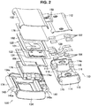
- FIG. 2 and FIG. 3 show a disassembled perspective view and a partial cross-sectional view, respectively, of the first segment 130 and the second segment 110 included in the electronic device 100.
- FIG. 2 and FIG. 3 show one first segment 130 and one second segment 110 linked to each other out of the links 102 included in the electronic device 100, and show the first segment 130a and the second segment 110a shown in FIG. 1 .
- the lower side in the drawing (the side where casings 114 and 134 are located) is located on the front side (the outside) at the time of wearing the electronic device 100.
- the lower side in the drawing corresponds to the front side of the electronic device 100.
- the front side or “the back side” refers to the front side (the outside) or the back side (the inside), respectively, at the time of wearing the electronic device 100.
- the width direction refers to a direction crossing the direction of arrangement of the plurality of links 102
- the “width” refers to the length in the width direction.
- the first segment 130 includes an arm unit 140 in an end portion on the second segment 110 side.
- the arm unit 140 is inserted in an insertion opening 116 provided in the second segment 110.
- a not-shown fixing pin is inserted in a pin insertion hole 140a provided in the arm unit 140 and a pin insertion hole 115 provided in the second segment 110 so as to penetrate through them, and thus the first segment 130 and the second segment 110 are linked together in a rotationally movable manner.
- the first segment 130 and the second segment 110 can rotationally move on the fixing pin as the rotation axis.
- the arm unit 140 of the first segment 130 comes into contact with a cover 112 or a casing 114 of the second segment 110, and thereby the range of rotational movement of the first segment 130 is regulated.
- a not-shown interconnection pattern is formed on an FPC 120 installed through the first segment 130 and the second segment 110. Portions of the interconnection pattern other than terminal portions to which connector portions 124 are electrically connected are coated with an insulating layer.
- an insulating resin such as a polycarbonate, an acrylic, polystyrene, polypropylene, or polyethylene terephthalate may be used.
- an electrically conductive material such as indium tin oxide, gold, or silver may be used.
- an insulating resin such as a polycarbonate, an acrylic, polystyrene, polypropylene, or polyethylene terephthalate may be used.
- an ultrathin FPC 120 is used so that the reaction force at the time of bending and stretching the first segment 130 and the second segment 110 does not become large.
- a secondary battery 174 as an example of the electronic component is housed. As described later, in the interior of the first segment 130, at least the secondary battery 174 and the electrical connection portion between the secondary battery 174 and the FPC 120 are placed in a water resistant space.
- the second segment 110 an electronic component is not housed, and the FPC 120 is pushed out while being bent to form a loosening portion 128.
- electrically conductive portions such as the interconnection pattern of the FPC 120 are not exposed, and there is no fear of short-circuiting, electric leakage, or corrosion. Therefore, a water resistant space is not present in the second segment 110.
- FIG. 4 is a schematic diagram showing a state where a second segment 110 is linked between two first segments 130.
- a water resistant space is provided in the first segment 130, whereas the second segment 110 is set outside the water resistant space.
- Each of the first segment 130 and the second segment 110 linked to each other can rotationally move on a rotation axis 190 of the link portion as the center.
- the FPC 120 is installed a little on the back side (the upper side in the drawing)
- the length of installation of the FPC 120 changes with the bending and stretching movement of the first segment 130 and the second segment 110.
- the loosening portion 128 is provided in the FPC 120 installed in the second segment 110, and the loosening portion 128 is deformed by loosening; thereby, the change in the length of installation of the FPC 120 can be followed.
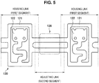
- FIG. 5 is a plan view showing an example of the planar configuration of the FPC 120 used for the electronic device 100 according to the embodiment.
- the FPC 120 is processed in a desired planar configuration by forming an interconnection pattern on the matrix, further forming an insulating layer, and then performing, for example, punching processing or the like.
- a frame portion 121 and an electrical connection portion 122 are provided in the portion installed in the first segment 130 of the FPC 120.
- the portion installed in the second segment 110 of the FPC 120 is divided into two sections, and each of them has a width smaller than the width of the frame portion 121.
- the portion installed in the second segment 110 of the FPC 120 is pushed out while being bent, and thereby the loosening portion 128 is formed.
- the not-shown interconnection pattern is formed so as to connect the terminal portions of the electrical connection portions 122 installed in two first segments 130, for example.
- the first segment 130 includes a casing 134 and a cover 132.
- the casing 134 has a housing portion 134a, and the secondary battery 174 is housed in the housing portion 134a.
- a first bonding member 164, the FPC 120, a second bonding member 162, and a water resistant cover 176 are stacked in this order. In this state, the cover 132 is put over from the back side, both ends of the cover 132 are locked to the casing 134, and the cover 132 is thus fixed to the casing 134.
- the FPC 120 has connector portions 124 electrically connected to terminals 174a of the secondary battery 174.
- the connector portion 124 is electrically connected to a terminal portion formed in the FPC 120, and the secondary battery 174 is electrically connected to the interconnection pattern of the FPC 120.
- the FPC 120 is fixed to an edge portion of the housing portion 134a of the casing 134 by the first bonding member 164.
- the FPC 120 installed in the first segment 130 has the frame portion 121 fixed to the casing 134 and the electrical connection portion 122 provided continuously from part of the frame portion 121 toward the inside of the frame portion 121.
- the frame portion 121 of the FPC 120 is fixed to the casing 134 by the first bonding member 164 in a frame-like shape that has a shape corresponding to the frame portion 121.
- the second bonding member 162 is stuck to the back surface side of the frame portion 121 of the FPC 120, and the water resistant cover 176 is fixed via the second bonding member 162.
- a water resistant adhesive paper sheet having an adhesive layer on both surfaces may be used.
- the first bonding member 164 and the second bonding member 162 are not particularly limited to the extent that they are a water resistant bonding sheet.
- a sheet made of a resin such as polyethylene terephthalate may be used as the water resistant cover 176.
- the first bonding member 164 and the second bonding member 162 are formed in a frame-like shape without a break; and their one surface is stuck to the frame portion 121 of the FPC 120, and their other surface is stuck to the water resistant cover 176 or the casing 134.
- the housing portion 134a of the casing 134 is formed by molding or the like, and does not have a gap or the like communicating with the outside except for the opening through which the secondary battery 174 is installed. Therefore, the space enclosed by the water resistant cover 176, the second bonding member 162, the frame portion 121 of the FPC 120, the first bonding member 164, and the housing portion 134a forms a water resistant space.
- the FPC 120 extending to the second segment 110 side is led out to the outside of the first segment 130 via the arm unit 140.
- the casing 134 and the cover 132 form a board installation opening 144 (see FIG. 3 ).
- the FPC 120 passes through the board installation opening 144 and is led out to the second segment 110 side.
- the FPC 120 installed in the board installation opening 144 is fixed to the casing 134 by a bonding sheet 184. That is, the FPC 120 is fixed to the casing 134 of the first segment 130 not only by the first bonding member 164 but also by the bonding sheet 184. Therefore, the behavior or stress of the FPC 120 in the second segment 110 is absorbed by the bonding sheet 184 in association with the bending and stretching movement of the first segment 130 and the second segment 110. Consequently, the stress transmitted to the first bonding member 164 and the second bonding member 162 that ensure the water resistance function can be reduced.
- the bonding sheet 184 has also a function as a buffer member that separates the FPC 120 from the edge of the casing 134 located at the exit of the board installation opening 144.
- the bonding sheet 184 is placed to extend up to an area facing the edge of the casing 134, and the FPC 120 is prevented from coming into direct contact with the edge of the casing 134 even when a bending deformation of the FPC 120 has occurred. Therefore, the FPC 120 can be prevented from receiving a flaw or a dent due to contact with the edge of the casing 134.
- a water resistant adhesive paper sheet having an adhesive layer on both surfaces may be used.
- a buffer member 182 is stuck to the surface on the cover 132 side of the FPC 120 installed in the board installation opening 144.
- the buffer member 182 has the function of separating the FPC 120 from the edge of the cover 132 located at the exit of the board installation opening 144.
- the buffer member 182 is installed up to an area facing the edge of the cover 132, and the FPC 120 is prevented from coming into direct contact with the edge of the cover 132 even when a bending deformation of the FPC 120 has occurred. Therefore, the FPC 120 can be prevented from receiving a flaw or a dent due to contact with the edge of the cover 132.
- a water resistant adhesive paper sheet having an adhesive layer on the surface on the FPC 120 side may be used.
- a bonding sheet having an adhesive layer on both surfaces may be used; thus, the FPC 120 may be fixed to the inner surface of the cover 132.
- a plurality of bonding sheets or buffer members may be placed to be stacked on at least one surface of the FPC 120.
- a support unit 150 that guides the led-out FPC 120 to the front side (the lower side in the drawing) is formed.
- the support unit 150 has the function of maintaining the direction of pushing-out of the loosening portion 128 of the FPC 120 formed in the second segment 110 to a fixed direction.
- the support unit 150 maintains the direction of pushing-out of the loosening portion 128 of the FPC 120 to the front side even when the first segment 130 and the second segment 110 are rotationally moved.
- the support unit 150 shown in FIG. 2 and FIG. 3 is formed by inclining an end portion of the cover 132 of the first segment 130 toward the direction of pushing-out of the loosening portion 128 of the FPC 120. Specifically, the support unit 150 is formed by warping an end portion of the cover 132 toward the FPC 120 side along the direction of installation of the FPC 120. Therefore, the FPC 120 is led out from the board installation opening 144 along the warped surface of the support unit 150, and extends toward the inner surface of a housing portion 114a of the casing 114 of the second segment 110.
- the inner surface of the cover 132 in which the support unit 150 is formed has a projecting portion 133 that projects further to the outside than the edge of, out of the inner surface of the board installation opening 144, the inner surface of the casing 134, which is located in the direction of pushing-out of the loosening portion 128, that is, on the front side.
- the support unit 150 is provided in the projecting portion 133, and the support unit 150 makes it easy for the FPC 120 to be guided to the front side.
- the second segment 110 includes the casing 114 and the cover 112.
- the casing 114 has the housing portion 114a leading to the insertion opening 116, and the FPC 120 is installed in the housing portion 114a.
- the FPC 120 is not fixed to the second segment 110, and is freely deformed by loosening.
- the cover 112 is put over from the back side, and the cover 112 is fixed to the casing 114 by not-shown screws. Water can enter the interior of the second segment 110 via the insertion opening 116; but since neither electronic components nor electrically conductive portions are exposed in the second segment 110, there is no fear of short-circuiting, electric leakage, corrosion, etc.
- a low friction layer 192 is provided on a position that is in the inner surface of the housing portion 114a of the casing 114 and that the FPC 120 can be in contact with.
- the low friction layer 192 is provided by, for example, sticking a sheet having a coefficient of friction smaller than the coefficient of friction of the surface of the casing 114 to the inner surface of the housing portion 114a.
- the low friction layer 192 can be formed by, for example, sticking a sheet containing a fluorine resin or forming a coating of a resin material containing a fluorine resin. In an embodiment of the present technology, the low friction layer 192 may be omitted.
- the loosening portion 128 of the FPC 120 formed in the second segment 110 will now be described in detail.
- the loosening portion 128 formed to be pushed out while being bent is formed in the FPC 120 placed in the second segment 110.
- the shape of the loosening portion 128 changes with the bending and stretching movement of the first segment 130 and the second segment 110.
- the loosening portion 128 is maintained in a state of being loosened in the entire region of the range of rotational movement of the first segment 130 and the second segment 110.
- the degree of loosening of the loosening portion 128 changes with the bending and stretching of the first segment 130 and the second segment 110.
- FIG. 6 to FIG. 8 are diagrams for describing the direction of pushing-out of the loosening portion 128 of the FPC 120 associated with the bending and stretching movement of the first segment 130 and the second segment 110.
- FIG. 6 is a schematic diagram showing the range of rotational movement of the first segment 130 relative to the second segment 110
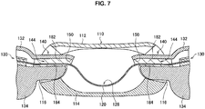
- FIG. 7 is a cross-sectional view showing a state where the first segment 130 and the second segment 110 are stretched.
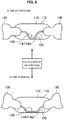
- FIG. 8 is a schematic diagram showing a manner in which the first segment 130 and the second segment 110 are being bent and stretched. In FIG. 6 to FIG. 8 , an example in which a second segment 110 is linked between two first segments 130 is shown.
- the support unit 150 that guides the FPC 120 led out from the first segment 130 to the casing 114 side is provided in the board installation opening 144 of the first segment 130. Therefore, in a state where the first segment 130 and the second segment 110 are stretched, the direction of pushing-out of the loosening portion 128 of the FPC 120 formed in the second segment 110 is maintained to the front side.
- the first segment 130 and the second segment 110 are bendable and stretchable so as to protrude to both the front side and the back side of the electronic device 100.
- the electronic device 100 according to the embodiment is used as the band of a wristwatch; when a state where the first segment 130 and the second segment 110 are stretched is taken as a reference, the range of rotational movement at the time when the first segment 130 is rotationally moved so that the front side of the electronic device 100 protrudes (angle ⁇ ) is larger than the range of rotational movement at the time when the first segment 130 is rotationally moved so that the back side of the electronic device 100 protrudes (angle a).
- the loosening portion 128 of the FPC 120 is line-symmetrical.
- the position where the FPC 120 is led out from the first segment 130 changes. Specifically, the distance between the position where the FPC 120 is led out from the first segment 130 and the inner surface of the casing 114 of the second segment 110 changes with the bending and stretching movement of the first segment 130 and the second segment 110.
- the loosening portion 128 is pressed against the inner surface of the casing 114 of the second segment 110, and the loosening shape of the loosening portion 128 is changed.
- the FPC 120 flexibly follows the bending and stretching movement of the first segment 130 and the second segment 110.
- the direction of pushing-out of the loosening portion 128 of the FPC 120 may be inverted when the first segment 130 and the second segment 110 are stretched.
- the direction of pushing-out of the loosening portion 128 is more likely to be inverted.
- the position of the apex of the loosening portion 128 can change with the bending and stretching movement of the first segment 130 and the second segment 110.
- the FPC 120 may be rubbed at the contact between the loosening portion 128 and the casing 114, and the FPC 120 may be damaged.
- the loosening portion 128 is pressed against the inner surface of the casing 114 already from the state where the first segment 130 and the second segment 110 are stretched, when the first segment 130 and the second segment 110 are bent so that the front side of the electronic device 100 protrudes, the loosening portion 128 of the FPC 120 is further pressed against the inner surface of the casing 114.
- the loosening portion 128 can be caused to lie along the shape of the inner surface of the housing portion 114a of the casing 114; thus, what is produced in association with the bending and stretching movement of the first segment 130 and the second segment 110 is not a change in the position of the apex of the loosening portion 128, but an increase or a decrease in the contact area between the loosening portion 128 and the inner surface of the casing 114. Therefore, the damage to the FPC 120 due to the rubbing together of the apex of the loosening portion 128 and the inner surface of the casing 114 of the second segment 110 can be suppressed.
- the low friction layer 192 is provided on a position that is in the inner surface of the casing 114 of the second segment 110 and can be in contact with the FPC 120. Therefore, even when a positional shift has occurred in a state where the loosening portion 128 and the inner surface of the casing 114 are in contact, the FPC 120 can be prevented from receiving scratches.
- the FPC 120 is separated from the edge of the exit of the board installation opening 144 by the buffer member 182 and the bonding sheet placed in the board installation opening 144 through which the FPC 120 is led out from the first segment 130. Therefore, even when the loosening shape of the loosening portion 128 of the FPC 120 has changed with the bending and stretching movement of the first segment 130 and the second segment 110, damage due to the contact of the first segment 130 and the FPC 120 can be prevented.
- the support unit 150 for maintaining the direction of pushing-out of the loosening portion 128 of the FPC 120 to a fixed direction may be variously modified. Two modification examples of the support unit will now be described.
- the support unit may have a configuration other than the modification examples illustrated below.
- FIG. 10 shows a support unit 150A according to a first modification example.
- the support unit 150A is formed by, not warping the projecting portion 133 of the cover 132 toward the FPC 120 side, standing an end portion of the projecting portion 133 toward the FPC 120 side.
- the FPC 120 led out from the first segment 130 can be guided in a prescribed direction.
- the thickness of the buffer member 182 may be increased. Thereby, at the contact position between the FPC 120 and the support unit 150A, the possibility of the occurrence of a flaw or a dent can be reduced.
- the position of formation of the support unit 150A formed to be stood from the cover 132 toward the FPC 120 side is not limited to an end portion of the cover 132.
- the support unit 150A may be stood from a position recessed from the end portion of the cover 132 toward the interior of the first segment 130.
- the support unit 150A formed to be stood toward the FPC 120 side may not be part of the cover 132, and may be formed to be inclined toward the FPC 120 side by, for example, increasing the thickness of the buffer member 182 or the bonding sheet, or stacking a plurality of buffer members 182 or bonding sheets partly.
- FIG. 11 shows a support unit 150B according to a second modification example.
- the support unit 150B is provided on the cover 112 of the second segment 110.
- the cover 112 of the second segment 110 is attached from the back side, and the support unit 150B provided on the inner surface of the cover 112 is placed on the back surface side of the FPC 120.
- the support unit 150B is stood on the FPC 120 side from the cover 112, and the tip (the lower end in the drawing) of the support unit 150B is located inside the bending of the loosening portion 128 of the FPC 120.
- the tip of the support unit 150B is located on the front side (the lower side in the drawing) with respect to the position of the FPC 120 led out from the first segment 130. Therefore, the direction of pushing-out of the loosening portion 128 of the FPC 120 can be prevented from being inverted in association with the bending and stretching movement of the first segment 130 and the second segment 110.
- the support unit 150B is provided on the cover 112 of the second segment 110, it is not necessary to provide a projecting portion in an end portion of the cover 132 of the first segment 130.
- the buffer member 182 or the bonding sheet 184 may be extended up to the edge of the cover 132 or the casing 134.
- the tip surface of the support unit 150B may be made a warped surface corresponding to the loosening shape, or a buffer member may be stuck to the tip surface of the support unit 150B.
- FIG. 12 shows the position of placement of the first bonding member 164 and the second bonding member 162 on the FPC 120 installed in the first segment 130 of the electronic device 100 according to the embodiment.
- FIG. 13 is a cross-sectional view taken along line X-X in FIG. 12 as seen in the direction of the arrows.
- the first bonding member 164 and the second bonding member 162 are installed seamlessly on the entire periphery of the frame portion 121 of the FPC 120. Thereby, the first bonding member 164 and the second bonding member 162 are stuck to the frame portion 121 of the FPC 120 in a state of surface contact without a gap. Although not shown, also for the portion between the second bonding member 162 and the water resistant cover 176 and the portion between the first bonding member 164 and the casing 134, the first bonding member 164 and the second bonding member 162 are similarly stuck to the respective members in a state of surface contact without a gap (see FIG. 2 ). Therefore, the area inside the position of adhesion of the first bonding member 164 and the second bonding member 162 in a frame-like shape is sealed without a gap, and a water resistant space is formed.
- the water resistance function of the area in the first segment 130 where the electronic component, the terminal portion of the FPC 120, etc. are placed is ensured. Thereby, short-circuiting, electric leakage, corrosion, etc. due to the adhesion of water to the secondary battery 174, the terminal portion and the connector portion 124 of the FPC 120, etc. existing in the water resistant space can be prevented.
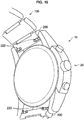
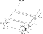
- FIG. 16 to FIG. 20 are illustration diagrams showing the connection structure between the electronic device 100 and the watch main body 20.
- FIG. 16 is a perspective view of the connection portion between the electronic device 100 and the watch main body 20 as viewed from the back side of the wristwatch 10.
- FIG. 17 is a perspective view showing the connecting link 200 of the electronic device 100
- FIG. 18 is a disassembled perspective view of the connecting link 200.
- FIG. 19 is a diagram schematically showing a cross section of the connecting link 200
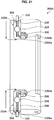
- FIG. 20 is a cross-sectional view showing a connecting component 220 using a lever pin 230.
- the electronic device 100 can be used as the band portion of the wristwatch 10, and is used to be connected to an arbitrary watch main body 20.
- the electronic device 100 includes a connecting link 200 equipped with a connecting component 220 in an end portion, and can be attached to and detached from the watch main body 20 by the user.
- a band-type electronic device 100 in which a plurality of links 102 are linked is attachable to and detachable from an arbitrary article, it is expected that the sense of incongruity with the portability or wearability of the electronic device 100 will be reduced, and the selection range of the position of wearing or attachment can be expanded.
- the connecting link 200 is, for example, a solid member made of stainless steel, titanium, or a resin material, and a hole 202 into which the connecting component 220 is press-fitted is formed on the surfaces on both sides in the width direction of the connecting link 200 (see FIG. 19 ).
- a width-direction trench 204 formed along the width direction is formed on the back surface of the connecting link 200.
- a bottom portion of the width-direction trench 204 communicates with the hole 202.
- the connecting component 220 is lightly press-fitted in the hole 202, and is thrust against the end of the hole 202.
- the connecting component 220 includes a cylinder 228 in a cylindrical shape of which one end is opened, a lever pin 230 inserted in the cylinder 228 and held in an axially movable manner in the cylinder 228, and a compression spring 234 installed between the closed end surface of the cylinder 228 and the rear end surface of the lever pin 230.
- the tip of the lever pin 230 protrudes from the cylinder 228 in a state where the lever pin 230 is biased in the axial direction by the compression spring 234.
- Not-shown engaging holes into each of which the tip of the lever pin 230 can be inserted are provided in the watch main body 20, and the lever pins 230 protruding on both sides in the width direction of the connecting link 200 are engaged with the engaging holes of the watch main body 20; thereby, the watch main body 20 and the electronic device 100 are connected together.
- the lever pin 230 has a lever portion 224 protruding outward in the diameter direction.
- the lever portion 224 is inserted in the cylinder 228 through a slit 228a provided along the axial direction.
- the slit 228a of the cylinder 228 is located in a bottom portion of the width-direction trench 204 provided in the connecting link 200, and the lever portion 224 is slidable through the width-direction trench 204 and the slit 228a.
- the tip (the protrusion end) of the lever portion 224 protrudes from the back surface of the connecting link 200. Therefore, the user may, for example, push the two lever portions 224 with the thumb and the forefinger inward in the width direction; thereby, the lever pins 230 can be recessed toward the interiors of the cylinders 228 against the biasing force of the compression springs 234.
- the electronic device 100 is attachable to and detachable from the watch main body 20 in a state where the tips of the lever pins 230 are recessed to near the positions of both end surfaces in the width direction of the connecting link 200.
- FIG. 21 shows a modification example of a connecting link 200A.
- the slit provided in the cylinder 228 of a connecting component 220A has an axial-direction slit portion 228Aa and a round-direction slit portion 228Ab.
- the width-direction trench 204 provided in the connecting link 200A has a lever housing portion 206 that is provided to extend in a direction orthogonal to the width-direction trench 204 to correspond to the round-direction slit portion 228Ab.
- the two lever portions 224 when attaching and detaching the electronic device 100 and the watch main body 20, the two lever portions 224 are moved inward along the axial-direction slit portions 228Aa, and are then slid in the round direction along the round-direction slit portions 228Ab.
- the lever portions 224 are locked in the round-direction slit portions 228Ab by the biasing force in the axial direction of the compression springs 234 provided in the connecting components 220A, and the lever pins 230 can be held in the state of being recessed even when the user has taken the fingers off.
- the two lever pins 230 can be attached to and detached from the watch main body 20 sequentially one by one, and the attachment and detachment operation of the electronic device 100 and the watch main body 20 can be made easy.
- the electronic device 100 Since the electronic device 100 according to the embodiment has such a connection structure, an arbitrarily selected watch main body 20 can be connected to a band-type electronic device 100 formed by a plurality of links 102 being linked. Therefore, an electronic device 100 with little sense of incongruity of the external appearance and the wearing condition can be obtained while an appropriate embodiment of the wristwatch 10 is employed in accordance with the usage environment, the use, the feeling of the user, etc. Furthermore, an arbitrary component having an appropriate function such as an accessory may be connected in place of the watch main body 20, and the selection range of the position of wearing or attachment of the electronic device 100 can be expanded.
- the electronic device 100 includes the support unit 150 for maintaining the direction of pushing-out of the loosening portion 128 of the FPC 120 formed in the second segment 110 to a fixed direction. Therefore, although the FPC 120 is installed throughout a plurality of links 102, the FPC 120 can be deformed by loosening to follow the bending and stretching movement of the electronic device 100 without being damaged.
- the loosening portion 128 of the FPC 120 is pressed against the inner surface of the second segment 110 from a state where the first segment 130 and the second segment 110 are stretched to a state where they are bent. Therefore, the FPC 120 can be prevented from being rubbed at the contact position between the loosening portion 128 of the FPC 120 and the inner surface of the second segment 110 and receiving a flaw.
- the electronic device 100 includes the low friction layer 192 on a position that is in the inner surface of the second segment 110 and that the loosening portion 128 of the FPC 120 is in contact with. Therefore, even when the contact position between the FPC 120 and the inner surface of the second segment 110 is shifted in association with the bending and stretching movement of the electronic device 100, the FPC 120 can be prevented from receiving scratches.
- the electronic device 100 includes the bonding sheet 184 and the buffer member 182 for separating the FPC 120 from the edge of the board installation opening 144 serving as the outlet port of the FPC 120 from the first segment 130. Therefore, when the loosening shape of the loosening portion 128 of the FPC 120 changes, the FPC 120 can be prevented from receiving a flaw or a dent due to contact with the edge of the board installation opening 144.
- the FPC 120 is fixed so as not to move in the first segment 130 in which the electronic component electrically connected to the FPC 120 is housed.
- the change in the length of installation of the FPC 120 associated with the bending and stretching movement of the electronic device 100 is absorbed by the loosening portion 128 in the second segment 110. Therefore, in the first segment 130, the water resistance function of the water resistant space where the electronic component and the electrically conductive portions are held can be ensured.
- the electronic device 100 is attachable to and detachable from an arbitrarily selected watch main body 20, accessory, etc. via the connecting link 200 linked in an end portion of the electronic device 100. Therefore, an electronic device 100 with little sense of incongruity of the external appearance and the wearing condition can be obtained while an arbitrary embodiment is employed in accordance with the usage environment, the use, the feeling of the user, etc.
- the selection range of the position of wearing or attachment of the electronic device 100 can be expanded.
Landscapes
- Engineering & Computer Science (AREA)
- Computer Hardware Design (AREA)
- Theoretical Computer Science (AREA)
- Physics & Mathematics (AREA)
- General Physics & Mathematics (AREA)
- Human Computer Interaction (AREA)
- General Engineering & Computer Science (AREA)
- Computer Networks & Wireless Communication (AREA)
- Telephone Set Structure (AREA)
- Insertion, Bundling And Securing Of Wires For Electric Apparatuses (AREA)
- Casings For Electric Apparatus (AREA)
Applications Claiming Priority (1)
| Application Number | Priority Date | Filing Date | Title |
|---|---|---|---|
| JP2015198075A JP6622048B2 (ja) | 2015-10-05 | 2015-10-05 | 電子機器 |
Publications (2)
| Publication Number | Publication Date |
|---|---|
| EP3153942A1 EP3153942A1 (en) | 2017-04-12 |
| EP3153942B1 true EP3153942B1 (en) | 2019-03-20 |
Family
ID=57288114
Family Applications (1)
| Application Number | Title | Priority Date | Filing Date |
|---|---|---|---|
| EP16190876.9A Active EP3153942B1 (en) | 2015-10-05 | 2016-09-27 | Wearable electronic device comprising a flexible circuit board |
Country Status (4)
| Country | Link |
|---|---|
| US (1) | US10503121B2 (enExample) |
| EP (1) | EP3153942B1 (enExample) |
| JP (1) | JP6622048B2 (enExample) |
| CN (1) | CN106560760B (enExample) |
Families Citing this family (13)
| Publication number | Priority date | Publication date | Assignee | Title |
|---|---|---|---|---|
| US20150241912A1 (en) * | 2014-02-21 | 2015-08-27 | Farshad Farjami | Wristband Accessories For A Wearable Computer |
| KR102420019B1 (ko) * | 2017-08-07 | 2022-07-12 | 삼성전자주식회사 | 웨어러블 디바이스 및 전자 기기 |
| CN107509352B (zh) * | 2017-08-25 | 2019-06-07 | 维沃移动通信有限公司 | 一种柔性电路板fpc的固定方法及移动终端 |
| JP6995574B2 (ja) * | 2017-11-10 | 2022-01-14 | 日本航空電子工業株式会社 | コネクタ |
| US12070108B2 (en) | 2017-11-20 | 2024-08-27 | Sony Corporation | Band device, wristwatch, and end piece |
| EP3712719B1 (en) * | 2019-03-20 | 2021-11-10 | Renata AG | A wristwatch with battery integrated in the clasp |
| WO2020242059A1 (en) * | 2019-05-29 | 2020-12-03 | Samsung Electronics Co., Ltd. | Electronic device including hinge structure |
| JP7281105B2 (ja) | 2020-11-20 | 2023-05-25 | カシオ計算機株式会社 | 連結体、バンド、および時計 |
| WO2023059018A1 (ko) * | 2021-10-06 | 2023-04-13 | 삼성전자 주식회사 | 연성 회로기판을 포함하는 전자 장치 |
| CN114356086A (zh) * | 2021-12-29 | 2022-04-15 | 北京有竹居网络技术有限公司 | 可调节指环装置 |
| WO2023149630A1 (ko) * | 2022-02-04 | 2023-08-10 | 삼성전자 주식회사 | 플렉서블 케이블을 포함하는 폴더블 전자 장치 |
| WO2024166626A1 (ja) * | 2023-02-06 | 2024-08-15 | ソニーグループ株式会社 | ウェアラブル装置、バックル構造 |
| CN118660401A (zh) * | 2024-01-31 | 2024-09-17 | 华为技术有限公司 | 柔性电路板及电子设备 |
Family Cites Families (13)
| Publication number | Priority date | Publication date | Assignee | Title |
|---|---|---|---|---|
| CH647916GA3 (enExample) * | 1981-08-25 | 1985-02-28 | ||
| JP2004172476A (ja) | 2002-11-21 | 2004-06-17 | Auto Network Gijutsu Kenkyusho:Kk | シールド機能を備えた導電路 |
| EP1579781B1 (fr) * | 2004-03-23 | 2006-12-13 | Comadur S.A. | Bracelet articulé comportant des maillons décoratifs enfilés sur une chaîne |
| JP2009288711A (ja) * | 2008-05-30 | 2009-12-10 | Kyocera Mita Corp | 画像形成装置 |
| SE535818C2 (sv) * | 2011-05-26 | 2013-01-02 | Stanley Wissmar | Ett mobilt armbandsur omfattande flera elektriska- och mikromekaniska komponenter som fungerar som en centralenhet för en mängd olika uppgifter |
| JP2013242365A (ja) * | 2012-05-18 | 2013-12-05 | Toppan Printing Co Ltd | フィルム発光型表示装置及びマルチフィルム発光型表示装置 |
| EP2898375B1 (fr) * | 2012-12-17 | 2016-05-18 | The Swatch Group Research and Development Ltd. | Dispositif electronique portable flexible |
| JP6064686B2 (ja) | 2013-03-07 | 2017-01-25 | 株式会社ジェイテクト | 電動パワーステアリング装置 |
| US9804639B2 (en) * | 2013-08-15 | 2017-10-31 | Apple Inc. | Hinged portable electronic device with display circuitry located in base |
| US9547341B2 (en) * | 2013-10-31 | 2017-01-17 | Sony Corporation | Information processing apparatus |
| US9720376B2 (en) * | 2014-11-18 | 2017-08-01 | Sony Corporation | Band type electronic device and substrate arrangement method |
| JP2016168289A (ja) * | 2015-03-16 | 2016-09-23 | カシオ計算機株式会社 | バンド及び電子機器 |
| KR20170004695A (ko) * | 2015-07-03 | 2017-01-11 | 엘지전자 주식회사 | 와치 타입 단말기 |
-
2015
- 2015-10-05 JP JP2015198075A patent/JP6622048B2/ja active Active
-
2016
- 2016-09-19 US US15/268,907 patent/US10503121B2/en active Active
- 2016-09-27 CN CN201610854394.6A patent/CN106560760B/zh active Active
- 2016-09-27 EP EP16190876.9A patent/EP3153942B1/en active Active
Non-Patent Citations (1)
| Title |
|---|
| None * |
Also Published As
| Publication number | Publication date |
|---|---|
| CN106560760A (zh) | 2017-04-12 |
| CN106560760B (zh) | 2021-06-15 |
| JP6622048B2 (ja) | 2019-12-18 |
| US20170097610A1 (en) | 2017-04-06 |
| US10503121B2 (en) | 2019-12-10 |
| JP2017073429A (ja) | 2017-04-13 |
| EP3153942A1 (en) | 2017-04-12 |
Similar Documents
| Publication | Publication Date | Title |
|---|---|---|
| EP3153942B1 (en) | Wearable electronic device comprising a flexible circuit board | |
| JP5722795B2 (ja) | 付属品の取付け装置 | |
| EP2889715B1 (en) | Wearable electronic device | |
| KR102131392B1 (ko) | 보호 커버 | |
| US8552294B2 (en) | Cable management apparatus | |
| EP2953329B1 (en) | Mobile phone flip leather case and smartphone | |
| KR102707941B1 (ko) | 키 조립체를 포함하는 전자 장치 | |
| CN107926118B (zh) | 电子装置 | |
| KR20170102310A (ko) | 멀티 피봇 힌지 커버 | |
| US20140306847A1 (en) | Antenna clip and electronic device employing the same | |
| EP2755367B1 (en) | Frame structure for preventing deformation, and electronic device including the same | |
| US9041867B2 (en) | Display casing and cover structure thereof | |
| US9693731B2 (en) | Electronic device | |
| US20250031811A1 (en) | Watchband for smart watch, and smart watch comprising same | |
| US8840416B2 (en) | Portable electronic device | |
| US20120268887A1 (en) | Flash drive | |
| KR20160137302A (ko) | 웨어러블 스마트 디바이스 | |
| CN203371841U (zh) | 片材部件、记事本用外套及电子设备用外壳 | |
| US8218101B2 (en) | Electronic device having an LCM with particular fixing element | |
| CN217524158U (zh) | 一种平板电脑保护套 | |
| TW201603679A (zh) | 電子總成及電子裝置 | |
| CN219959455U (zh) | 线夹弹片及电子设备 | |
| US20240405463A1 (en) | Connector and electronic device including same | |
| TWI596834B (zh) | Card connector | |
| CN209767621U (zh) | 保护壳以及电子设备 |
Legal Events
| Date | Code | Title | Description |
|---|---|---|---|
| PUAI | Public reference made under article 153(3) epc to a published international application that has entered the european phase |
Free format text: ORIGINAL CODE: 0009012 |
|
| STAA | Information on the status of an ep patent application or granted ep patent |
Free format text: STATUS: REQUEST FOR EXAMINATION WAS MADE |
|
| 17P | Request for examination filed |
Effective date: 20161027 |
|
| AK | Designated contracting states |
Kind code of ref document: A1 Designated state(s): AL AT BE BG CH CY CZ DE DK EE ES FI FR GB GR HR HU IE IS IT LI LT LU LV MC MK MT NL NO PL PT RO RS SE SI SK SM TR |
|
| AX | Request for extension of the european patent |
Extension state: BA ME |
|
| STAA | Information on the status of an ep patent application or granted ep patent |
Free format text: STATUS: EXAMINATION IS IN PROGRESS |
|
| 17Q | First examination report despatched |
Effective date: 20180215 |
|
| RIC1 | Information provided on ipc code assigned before grant |
Ipc: G04G 17/06 20060101ALI20180814BHEP Ipc: G06F 1/16 20060101AFI20180814BHEP |
|
| GRAP | Despatch of communication of intention to grant a patent |
Free format text: ORIGINAL CODE: EPIDOSNIGR1 |
|
| STAA | Information on the status of an ep patent application or granted ep patent |
Free format text: STATUS: GRANT OF PATENT IS INTENDED |
|
| INTG | Intention to grant announced |
Effective date: 20181008 |
|
| GRAS | Grant fee paid |
Free format text: ORIGINAL CODE: EPIDOSNIGR3 |
|
| GRAA | (expected) grant |
Free format text: ORIGINAL CODE: 0009210 |
|
| STAA | Information on the status of an ep patent application or granted ep patent |
Free format text: STATUS: THE PATENT HAS BEEN GRANTED |
|
| AK | Designated contracting states |
Kind code of ref document: B1 Designated state(s): AL AT BE BG CH CY CZ DE DK EE ES FI FR GB GR HR HU IE IS IT LI LT LU LV MC MK MT NL NO PL PT RO RS SE SI SK SM TR |
|
| REG | Reference to a national code |
Ref country code: GB Ref legal event code: FG4D |
|
| REG | Reference to a national code |
Ref country code: CH Ref legal event code: EP |
|
| REG | Reference to a national code |
Ref country code: DE Ref legal event code: R096 Ref document number: 602016011225 Country of ref document: DE |
|
| REG | Reference to a national code |
Ref country code: AT Ref legal event code: REF Ref document number: 1111180 Country of ref document: AT Kind code of ref document: T Effective date: 20190415 |
|
| REG | Reference to a national code |
Ref country code: IE Ref legal event code: FG4D |
|
| RAP2 | Party data changed (patent owner data changed or rights of a patent transferred) |
Owner name: SONY CORPORATION |
|
| REG | Reference to a national code |
Ref country code: NL Ref legal event code: FP |
|
| PG25 | Lapsed in a contracting state [announced via postgrant information from national office to epo] |
Ref country code: FI Free format text: LAPSE BECAUSE OF FAILURE TO SUBMIT A TRANSLATION OF THE DESCRIPTION OR TO PAY THE FEE WITHIN THE PRESCRIBED TIME-LIMIT Effective date: 20190320 Ref country code: SE Free format text: LAPSE BECAUSE OF FAILURE TO SUBMIT A TRANSLATION OF THE DESCRIPTION OR TO PAY THE FEE WITHIN THE PRESCRIBED TIME-LIMIT Effective date: 20190320 Ref country code: LT Free format text: LAPSE BECAUSE OF FAILURE TO SUBMIT A TRANSLATION OF THE DESCRIPTION OR TO PAY THE FEE WITHIN THE PRESCRIBED TIME-LIMIT Effective date: 20190320 Ref country code: NO Free format text: LAPSE BECAUSE OF FAILURE TO SUBMIT A TRANSLATION OF THE DESCRIPTION OR TO PAY THE FEE WITHIN THE PRESCRIBED TIME-LIMIT Effective date: 20190620 |
|
| REG | Reference to a national code |
Ref country code: LT Ref legal event code: MG4D |
|
| PG25 | Lapsed in a contracting state [announced via postgrant information from national office to epo] |
Ref country code: GR Free format text: LAPSE BECAUSE OF FAILURE TO SUBMIT A TRANSLATION OF THE DESCRIPTION OR TO PAY THE FEE WITHIN THE PRESCRIBED TIME-LIMIT Effective date: 20190621 Ref country code: LV Free format text: LAPSE BECAUSE OF FAILURE TO SUBMIT A TRANSLATION OF THE DESCRIPTION OR TO PAY THE FEE WITHIN THE PRESCRIBED TIME-LIMIT Effective date: 20190320 Ref country code: BG Free format text: LAPSE BECAUSE OF FAILURE TO SUBMIT A TRANSLATION OF THE DESCRIPTION OR TO PAY THE FEE WITHIN THE PRESCRIBED TIME-LIMIT Effective date: 20190620 Ref country code: RS Free format text: LAPSE BECAUSE OF FAILURE TO SUBMIT A TRANSLATION OF THE DESCRIPTION OR TO PAY THE FEE WITHIN THE PRESCRIBED TIME-LIMIT Effective date: 20190320 Ref country code: HR Free format text: LAPSE BECAUSE OF FAILURE TO SUBMIT A TRANSLATION OF THE DESCRIPTION OR TO PAY THE FEE WITHIN THE PRESCRIBED TIME-LIMIT Effective date: 20190320 |
|
| REG | Reference to a national code |
Ref country code: AT Ref legal event code: MK05 Ref document number: 1111180 Country of ref document: AT Kind code of ref document: T Effective date: 20190320 |
|
| PG25 | Lapsed in a contracting state [announced via postgrant information from national office to epo] |
Ref country code: CZ Free format text: LAPSE BECAUSE OF FAILURE TO SUBMIT A TRANSLATION OF THE DESCRIPTION OR TO PAY THE FEE WITHIN THE PRESCRIBED TIME-LIMIT Effective date: 20190320 Ref country code: ES Free format text: LAPSE BECAUSE OF FAILURE TO SUBMIT A TRANSLATION OF THE DESCRIPTION OR TO PAY THE FEE WITHIN THE PRESCRIBED TIME-LIMIT Effective date: 20190320 Ref country code: RO Free format text: LAPSE BECAUSE OF FAILURE TO SUBMIT A TRANSLATION OF THE DESCRIPTION OR TO PAY THE FEE WITHIN THE PRESCRIBED TIME-LIMIT Effective date: 20190320 Ref country code: AL Free format text: LAPSE BECAUSE OF FAILURE TO SUBMIT A TRANSLATION OF THE DESCRIPTION OR TO PAY THE FEE WITHIN THE PRESCRIBED TIME-LIMIT Effective date: 20190320 Ref country code: PT Free format text: LAPSE BECAUSE OF FAILURE TO SUBMIT A TRANSLATION OF THE DESCRIPTION OR TO PAY THE FEE WITHIN THE PRESCRIBED TIME-LIMIT Effective date: 20190720 Ref country code: SK Free format text: LAPSE BECAUSE OF FAILURE TO SUBMIT A TRANSLATION OF THE DESCRIPTION OR TO PAY THE FEE WITHIN THE PRESCRIBED TIME-LIMIT Effective date: 20190320 Ref country code: IT Free format text: LAPSE BECAUSE OF FAILURE TO SUBMIT A TRANSLATION OF THE DESCRIPTION OR TO PAY THE FEE WITHIN THE PRESCRIBED TIME-LIMIT Effective date: 20190320 Ref country code: EE Free format text: LAPSE BECAUSE OF FAILURE TO SUBMIT A TRANSLATION OF THE DESCRIPTION OR TO PAY THE FEE WITHIN THE PRESCRIBED TIME-LIMIT Effective date: 20190320 |
|
| PG25 | Lapsed in a contracting state [announced via postgrant information from national office to epo] |
Ref country code: PL Free format text: LAPSE BECAUSE OF FAILURE TO SUBMIT A TRANSLATION OF THE DESCRIPTION OR TO PAY THE FEE WITHIN THE PRESCRIBED TIME-LIMIT Effective date: 20190320 Ref country code: SM Free format text: LAPSE BECAUSE OF FAILURE TO SUBMIT A TRANSLATION OF THE DESCRIPTION OR TO PAY THE FEE WITHIN THE PRESCRIBED TIME-LIMIT Effective date: 20190320 |
|
| PG25 | Lapsed in a contracting state [announced via postgrant information from national office to epo] |
Ref country code: IS Free format text: LAPSE BECAUSE OF FAILURE TO SUBMIT A TRANSLATION OF THE DESCRIPTION OR TO PAY THE FEE WITHIN THE PRESCRIBED TIME-LIMIT Effective date: 20190720 Ref country code: AT Free format text: LAPSE BECAUSE OF FAILURE TO SUBMIT A TRANSLATION OF THE DESCRIPTION OR TO PAY THE FEE WITHIN THE PRESCRIBED TIME-LIMIT Effective date: 20190320 |
|
| REG | Reference to a national code |
Ref country code: DE Ref legal event code: R097 Ref document number: 602016011225 Country of ref document: DE |
|
| PLBE | No opposition filed within time limit |
Free format text: ORIGINAL CODE: 0009261 |
|
| STAA | Information on the status of an ep patent application or granted ep patent |
Free format text: STATUS: NO OPPOSITION FILED WITHIN TIME LIMIT |
|
| PG25 | Lapsed in a contracting state [announced via postgrant information from national office to epo] |
Ref country code: DK Free format text: LAPSE BECAUSE OF FAILURE TO SUBMIT A TRANSLATION OF THE DESCRIPTION OR TO PAY THE FEE WITHIN THE PRESCRIBED TIME-LIMIT Effective date: 20190320 |
|
| 26N | No opposition filed |
Effective date: 20200102 |
|
| PG25 | Lapsed in a contracting state [announced via postgrant information from national office to epo] |
Ref country code: SI Free format text: LAPSE BECAUSE OF FAILURE TO SUBMIT A TRANSLATION OF THE DESCRIPTION OR TO PAY THE FEE WITHIN THE PRESCRIBED TIME-LIMIT Effective date: 20190320 |
|
| PG25 | Lapsed in a contracting state [announced via postgrant information from national office to epo] |
Ref country code: TR Free format text: LAPSE BECAUSE OF FAILURE TO SUBMIT A TRANSLATION OF THE DESCRIPTION OR TO PAY THE FEE WITHIN THE PRESCRIBED TIME-LIMIT Effective date: 20190320 |
|
| REG | Reference to a national code |
Ref country code: DE Ref legal event code: R081 Ref document number: 602016011225 Country of ref document: DE Owner name: SONY CORPORATION, JP Free format text: FORMER OWNER: SONY MOBILE COMMUNICATIONS INC., TOKYO, JP |
|
| PG25 | Lapsed in a contracting state [announced via postgrant information from national office to epo] |
Ref country code: MC Free format text: LAPSE BECAUSE OF FAILURE TO SUBMIT A TRANSLATION OF THE DESCRIPTION OR TO PAY THE FEE WITHIN THE PRESCRIBED TIME-LIMIT Effective date: 20190320 |
|
| REG | Reference to a national code |
Ref country code: CH Ref legal event code: PL |
|
| PG25 | Lapsed in a contracting state [announced via postgrant information from national office to epo] |
Ref country code: LU Free format text: LAPSE BECAUSE OF NON-PAYMENT OF DUE FEES Effective date: 20190927 Ref country code: IE Free format text: LAPSE BECAUSE OF NON-PAYMENT OF DUE FEES Effective date: 20190927 Ref country code: LI Free format text: LAPSE BECAUSE OF NON-PAYMENT OF DUE FEES Effective date: 20190930 Ref country code: CH Free format text: LAPSE BECAUSE OF NON-PAYMENT OF DUE FEES Effective date: 20190930 |
|
| REG | Reference to a national code |
Ref country code: BE Ref legal event code: MM Effective date: 20190930 |
|
| PG25 | Lapsed in a contracting state [announced via postgrant information from national office to epo] |
Ref country code: BE Free format text: LAPSE BECAUSE OF NON-PAYMENT OF DUE FEES Effective date: 20190930 |
|
| PG25 | Lapsed in a contracting state [announced via postgrant information from national office to epo] |
Ref country code: CY Free format text: LAPSE BECAUSE OF FAILURE TO SUBMIT A TRANSLATION OF THE DESCRIPTION OR TO PAY THE FEE WITHIN THE PRESCRIBED TIME-LIMIT Effective date: 20190320 |
|
| PG25 | Lapsed in a contracting state [announced via postgrant information from national office to epo] |
Ref country code: HU Free format text: LAPSE BECAUSE OF FAILURE TO SUBMIT A TRANSLATION OF THE DESCRIPTION OR TO PAY THE FEE WITHIN THE PRESCRIBED TIME-LIMIT; INVALID AB INITIO Effective date: 20160927 Ref country code: MT Free format text: LAPSE BECAUSE OF FAILURE TO SUBMIT A TRANSLATION OF THE DESCRIPTION OR TO PAY THE FEE WITHIN THE PRESCRIBED TIME-LIMIT Effective date: 20190320 |
|
| PG25 | Lapsed in a contracting state [announced via postgrant information from national office to epo] |
Ref country code: MK Free format text: LAPSE BECAUSE OF FAILURE TO SUBMIT A TRANSLATION OF THE DESCRIPTION OR TO PAY THE FEE WITHIN THE PRESCRIBED TIME-LIMIT Effective date: 20190320 |
|
| P01 | Opt-out of the competence of the unified patent court (upc) registered |
Effective date: 20230527 |
|
| PGFP | Annual fee paid to national office [announced via postgrant information from national office to epo] |
Ref country code: NL Payment date: 20240820 Year of fee payment: 9 |
|
| PGFP | Annual fee paid to national office [announced via postgrant information from national office to epo] |
Ref country code: GB Payment date: 20240820 Year of fee payment: 9 |
|
| PGFP | Annual fee paid to national office [announced via postgrant information from national office to epo] |
Ref country code: FR Payment date: 20240820 Year of fee payment: 9 |
|
| PGFP | Annual fee paid to national office [announced via postgrant information from national office to epo] |
Ref country code: DE Payment date: 20250820 Year of fee payment: 10 |