EP3136833A1 - Optimierungsprogramm und montageoperationssystem - Google Patents
Optimierungsprogramm und montageoperationssystem Download PDFInfo
- Publication number
- EP3136833A1 EP3136833A1 EP14890427.9A EP14890427A EP3136833A1 EP 3136833 A1 EP3136833 A1 EP 3136833A1 EP 14890427 A EP14890427 A EP 14890427A EP 3136833 A1 EP3136833 A1 EP 3136833A1
- Authority
- EP
- European Patent Office
- Prior art keywords
- mounting
- work
- mounting work
- electronic components
- circuit pattern
- Prior art date
- Legal status (The legal status is an assumption and is not a legal conclusion. Google has not performed a legal analysis and makes no representation as to the accuracy of the status listed.)
- Granted
Links
Images



Classifications
-
- H—ELECTRICITY
- H05—ELECTRIC TECHNIQUES NOT OTHERWISE PROVIDED FOR
- H05K—PRINTED CIRCUITS; CASINGS OR CONSTRUCTIONAL DETAILS OF ELECTRIC APPARATUS; MANUFACTURE OF ASSEMBLAGES OF ELECTRICAL COMPONENTS
- H05K13/00—Apparatus or processes specially adapted for manufacturing or adjusting assemblages of electric components
- H05K13/04—Mounting of components, e.g. of leadless components
-
- H—ELECTRICITY
- H05—ELECTRIC TECHNIQUES NOT OTHERWISE PROVIDED FOR
- H05K—PRINTED CIRCUITS; CASINGS OR CONSTRUCTIONAL DETAILS OF ELECTRIC APPARATUS; MANUFACTURE OF ASSEMBLAGES OF ELECTRICAL COMPONENTS
- H05K13/00—Apparatus or processes specially adapted for manufacturing or adjusting assemblages of electric components
- H05K13/04—Mounting of components, e.g. of leadless components
- H05K13/0452—Mounting machines or lines comprising a plurality of tools for guiding different components to the same mounting place
-
- H—ELECTRICITY
- H05—ELECTRIC TECHNIQUES NOT OTHERWISE PROVIDED FOR
- H05K—PRINTED CIRCUITS; CASINGS OR CONSTRUCTIONAL DETAILS OF ELECTRIC APPARATUS; MANUFACTURE OF ASSEMBLAGES OF ELECTRICAL COMPONENTS
- H05K13/00—Apparatus or processes specially adapted for manufacturing or adjusting assemblages of electric components
- H05K13/04—Mounting of components, e.g. of leadless components
- H05K13/0495—Mounting of components, e.g. of leadless components having a plurality of work-stations
-
- H—ELECTRICITY
- H05—ELECTRIC TECHNIQUES NOT OTHERWISE PROVIDED FOR
- H05K—PRINTED CIRCUITS; CASINGS OR CONSTRUCTIONAL DETAILS OF ELECTRIC APPARATUS; MANUFACTURE OF ASSEMBLAGES OF ELECTRICAL COMPONENTS
- H05K13/00—Apparatus or processes specially adapted for manufacturing or adjusting assemblages of electric components
- H05K13/08—Monitoring manufacture of assemblages
-
- H—ELECTRICITY
- H05—ELECTRIC TECHNIQUES NOT OTHERWISE PROVIDED FOR
- H05K—PRINTED CIRCUITS; CASINGS OR CONSTRUCTIONAL DETAILS OF ELECTRIC APPARATUS; MANUFACTURE OF ASSEMBLAGES OF ELECTRICAL COMPONENTS
- H05K13/00—Apparatus or processes specially adapted for manufacturing or adjusting assemblages of electric components
- H05K13/08—Monitoring manufacture of assemblages
- H05K13/085—Production planning, e.g. of allocation of products to machines, of mounting sequences at machine or facility level
-
- Y—GENERAL TAGGING OF NEW TECHNOLOGICAL DEVELOPMENTS; GENERAL TAGGING OF CROSS-SECTIONAL TECHNOLOGIES SPANNING OVER SEVERAL SECTIONS OF THE IPC; TECHNICAL SUBJECTS COVERED BY FORMER USPC CROSS-REFERENCE ART COLLECTIONS [XRACs] AND DIGESTS
- Y10—TECHNICAL SUBJECTS COVERED BY FORMER USPC
- Y10T—TECHNICAL SUBJECTS COVERED BY FORMER US CLASSIFICATION
- Y10T29/00—Metal working
- Y10T29/53—Means to assemble or disassemble
- Y10T29/5313—Means to assemble electrical device
- Y10T29/53174—Means to fasten electrical component to wiring board, base, or substrate
-
- Y—GENERAL TAGGING OF NEW TECHNOLOGICAL DEVELOPMENTS; GENERAL TAGGING OF CROSS-SECTIONAL TECHNOLOGIES SPANNING OVER SEVERAL SECTIONS OF THE IPC; TECHNICAL SUBJECTS COVERED BY FORMER USPC CROSS-REFERENCE ART COLLECTIONS [XRACs] AND DIGESTS
- Y10—TECHNICAL SUBJECTS COVERED BY FORMER USPC
- Y10T—TECHNICAL SUBJECTS COVERED BY FORMER US CLASSIFICATION
- Y10T29/00—Metal working
- Y10T29/53—Means to assemble or disassemble
- Y10T29/5313—Means to assemble electrical device
- Y10T29/53187—Multiple station assembly apparatus
Definitions
- the present invention relates to a mounting work system in which mounting work is sequentially performed on circuit substrates being conveyed, and an optimization program that optimizes the mounting work for each work machine in the system.
- a mounting work system is usually provided with multiple mounting work machines lined up, and circuit substrates are conveyed from an upstream side of the multiple mounting work machines to a downstream side.
- mounting work of mounting multiple electronic components on the circuit substrate is divided between each of the multiple mounting work machines.
- mounting procedures for mounting the multiple electronic components on the circuit substrate (hereinafter also referred to simply as "work procedure") are set as work data to the multiple mounting work machines.
- circuit substrates there are circuit substrates that are provided with multiple boards on one circuit substrate, in which multiple electronic circuit board patterns (hereinafter sometimes referred to as “circuit pattern") on which multiple electronic components are to be mounted are provided; and these multiple-board substrates sometimes include a circuit pattern that is not in good condition (hereinafter sometimes referred to as "defective circuit pattern").
- circuit pattern multiple electronic circuit board patterns
- these multiple-board substrates sometimes include a circuit pattern that is not in good condition
- mounting work to the defective circuit pattern can be skipped during mounting work, and it is desirable to improve throughput of substrate work system 10 as much as possible.
- development has progressed of work procedure settings means for improving throughput when performing mounting work on multiple-board substrates that include a defective circuit pattern.
- the present invention takes account of such circumstances and an object thereof is to further improve the throughput when performing mounting work on multiple-board substrates that include a defective circuit pattern.
- an optimization program for optimizing work of mounting electronic components including: a setting means that sets a mounting work procedure of mounting electronic components to an electronic circuit board pattern for each of multiple mounting work machines such that mounting work of multiple components to each of multiple of the electronic circuit board patterns is performed by all of the multiple mounting work machines, the optimization program being for a mounting work system provided with multiple of the mounting work machines lined up in a row, with multiple-board printed panels being conveyed in the mounting work system from an upstream side of the multiple mounting work machines to a downstream side, the multiple-board printed panel being defined as a panel with multiple boards provided with an electronic circuit board pattern to be mounted with multiple of the electronic components.
- the optimization program disclosed in claim 2 is the optimization program according to claim 1, wherein the setting means sets the mounting work procedure of mounting electronic components to the electronic circuit board pattern for each of the multiple mounting work machines such that the total time for work of mounting the electronic components to the electronic circuit board pattern is equalized for each of the multiple mounting work machines.
- the optimization program disclosed in claim 3 is the optimization program according to claim 1 or 2, wherein the setting means sets the mounting work procedure of mounting electronic components to the electronic circuit board pattern for each of the multiple mounting work machines according to the quantity of electronic components per unit of time to be mounted to the electronic circuit board pattern by each of the multiple mounting work machines.
- a mounting work system including: multiple mounting work machines lined up in a row; and a control device that controls operation of the multiple mounting work machines, wherein multiple-board printed panels are conveyed in the mounting work system from an upstream side of the multiple mounting work machines to a downstream side, the multiple-board printed panel being defined as a panel with multiple boards provided with an electronic circuit board pattern to be mounted with multiple of the electronic component, and wherein the control device controls operation of the multiple mounting work machines such that the electronic components are mounted the electronic circuit board pattern according to a mounting work procedure of mounting electronic components to the electronic circuit board pattern for each of the multiple mounting work machines such that work of mounting the multiple electronic components of each of the multiple electronic circuit board patterns is performed by all of the multiple mounting work machines.
- the mounting work procedure of mounting electronic components to an electronic circuit board pattern for each of multiple mounting work machines is set such that work of mounting multiple electronic components onto each of the multiple electronic circuit board patterns is performed by all of the multiple mounting work machines. Accordingly, in a case in which mounting work onto a defective circuit pattern is not performed, for all of the mounting work machines, the time required for mounting by the mounting work machine is reduced by the time required for mounting work of the defective circuit pattern, thus the throughput of substrate work system 10 is improved.
- the mounting work procedure of mounting electronic components to the electronic circuit board pattern for each of the multiple mounting work machines is set such that the total time for work of mounting the electronic components to the electronic circuit board pattern is equalized for each of the multiple mounting work machines.
- the mounting work procedure of mounting electronic components to the electronic circuit board pattern for each of the multiple mounting work machines is set according to the quantity of electronic components per unit of time to be mounted to the electronic circuit board pattern by each of the multiple mounting work machines.
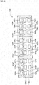
- Fig. 1 shows substrate work system 10.
- System 10 shown in fig. 1 is for mounting electronic components on a circuit substrate.
- Substrate work system 10 is configured from four electronic component mounting devices (hereinafter sometimes referred to as "mounting devices") 12.
- the four mounting devices 12 are in a line adjacent to each other.
- the X-axis direction refers to the direction in which mounting devices 12 are lined up
- the Y-axis direction refers to the horizontal direction orthogonal to the X-axis direction.
- mounting device 12 includes system base 14, and two mounters 16 arranged adjacent to each other on system base 14.
- Each mounter 16 primarily includes mounter body 20, conveyance device 22, mounting head 24, mounting head moving device (hereinafter sometimes abbreviated to "moving device") 26, and supply device 28.
- Mounter body 20 is configured from frame 30 and beam 32 that is mounted on the frame 30.
- Conveyance device 22 is provided with two conveyor devices 40 and 42.
- the two conveyor devices 40 and 42 are parallel to each other and are provided on frame 30 extending in the X-axis direction.
- Each of the two conveyor devices 40 and 42 conveys circuit substrates held by conveyor device 40 and 42 in the X-axis direction using electromagnetic motor (refer to fig. 3 ) 46.
- the circuit substrate is fixedly held at a predetermined position by board holding device (refer to fig. 3 ) 48.
- Moving device 26 is an XY robot type moving device.
- Moving device 26 is provided with electromagnetic motor (refer to fig. 3 ) 52 that slides slider 50 in the X-axis direction, and electromagnetic motor (refer to fig. 3 ) 54 that slides slider 50 in the Y-axis direction.
- Mounting head 24 is attached to slider 50, and mounting head 24 is moved to any position on frame 30 by the operation of the two electromagnetic motors 52 and 54.
- Supply device 28 is a feeder type supply device and is provided on the front end of frame 30.
- Supply device 28 has tape feeders 70.
- Tape feeders 70 house taped components in a wound state. Taped components are electronic components that have been put into tape. Tape feeders 70 deliver the taped components using indexing device (refer to fig. 3 ) 76. Accordingly, feeder type supply device 28 supplies an electronic component to a supply position through the feeding delivery of the taped components. Tape feeders 70 can be removed from and attached to frame 30 to facilitate the exchange of electronic components and so on.
- Mounting head 24 mounts electronic components on a circuit substrate.
- Mounting head 24 includes suction nozzle 78 that is provided on a lower end face of the mounting head.
- Suction nozzle 78 is connected to positive/negative pressure supply device (refer to fig. 3 ) 80 via a negative pressure air/positive pressure air supply passage.
- Suction nozzle 78 picks up and holds an electronic component using negative pressure, and releases the held electronic component using positive pressure.
- mounting head 24 has nozzle raising/lowering device (refer to fig. 3 ) 82 that raises/lowers suction nozzle 78.
- Mounting head 24 changes the position of the held electronic component in a vertical direction by nozzle raising/lowering device 82.
- suction nozzles 78 can be attached to and removed from mounting head 24, and can be changed based on things such as the size and shape of the electronic components.
- substrate work system 10 is provided with control device 90.
- Control device 90 is provided with controller 92 and multiple drive circuits 96. Multiple drive circuits 96 are connected to electromagnetic motors 46, 52, and 54, substrate holding device 48, indexing device 76, positive/negative pressure supply device 80, and nozzle raising/lowering device 82.
- Controller 92 is provided with a CPU, ROM, RAM, and so on, is formed mainly from a computer, and is connected to the multiple drive circuits 96. By this, operation of conveyance device 22, moving device 26, and so on is controlled by controller 92.
- circuit substrates are conveyed by conveyance device 22 inside the eight mounters 16, and electronic components are mounted on the circuit substrates by each mounter 16.
- a circuit substrate is loaded into the mounter 16 arranged at the most upstream position of the eight mounters 16. Then, based on commands of controller 92, the circuit substrate is conveyed to a work position, and fixedly held at that position by substrate holding device 48. Also, based on commands of controller 92, tape feeders 70 feed taped components and supply electronic components to supply positions. Then, based on commands of controller 92, mounting head 24 moves above the supply position of the electronic component and picks up and holds the electronic component using suction nozzle 78. Continuing, mounting head 24 moves above the circuit substrate and mounts the held electronic component on the circuit substrate. When work of mounting electronic components on the circuit substrate is complete, the circuit substrate is conveyed downstream and loaded into mounter 16 positioned on the downstream side. The above work is performed consecutively at each mounter 16 to produce circuit substrates mounted with electronic components.
- mounting procedure for mounting multiple-board substrates
- production of circuit substrates is performed according to the above procedure; because multiple electronic components are mounted on a circuit substrate, mounting work of mounting multiple electronic components on the circuit substrate is divided between each of the multiple mounters 16 that configure substrate work system 10.
- mounting procedures for mounting the multiple electronic components on the circuit substrate (hereinafter also referred to simply as “mounting procedure") are set as work data to the multiple mounters 16. Described below is a work procedure when a circuit substrate being produced is a multiple-board substrate.
- circuit pattern multiple electronic circuit board patterns (hereinafter referred to as "circuit pattern") on which multiple electronic components are to be mounted are provided; specifically, for example, on multiple-board substrate 100 shown in fig. 4 , there are three circuit patterns 102, with nine electronic components 104 mounted on each circuit pattern 102.
- Substrate work system 10 includes eight mounters 16; to describe setting a work procedure to the eight mounters 16 would be very complex, so description is given of setting a work procedure for three mounters 16 that perform mounting work with respect to multiple-board substrate 100. To distinguish between the three mounters 16, they are sometimes referred to as first mounter 16a, second mounter 16b, and third mounter 16c. Also, to distinguish between the three circuit patterns 102, they are sometimes referred to as first circuit pattern 102a, second circuit pattern 102b, and third circuit pattern 102c.
- first electronic component 104a second electronic component 104b, third electronic component 104c, fourth electronic component 104d, fifth electronic component 104e, sixth electronic component 104f, seventh electronic component 104g, eighth electronic component 104h, and ninth electronic component 104i.
- a work procedure for nine electronic components 104 to first circuit pattern 102a may be set to first mounter 16a
- a work procedure for nine electronic components 104 to second circuit pattern 102b may be set to second mounter 16b
- a work procedure for nine electronic components 104 to third circuit pattern 102c may be set to first mounter 16c. That is, a work procedure for electronic components surrounded by the dashed line in fig. 4 may be set to first mounter 16a, a work procedure for electronic components surrounded by the single-dashed solid line in fig.
- a work procedure for electronic components surrounded by the double-dashed solid line in fig. 4 may be set to third mounter 16c.
- one or more of the three circuit patterns 102 of multiple-board substrate 100 is a defective circuit pattern.
- mounting work is not performed with respect to defective circuit pattern (hereinafter sometimes referred to as "defective circuit pattern) 102. That is, in a case in which second circuit pattern 102 is a defective circuit pattern, mounting work is performed by first mounter 16a and third mounter 16c without being performed by second mounter 16b.
- the throughput of substrate work system 10 can be thought to improve due to mounting work not being performed by second mounter 16b.
- an upstream mounter 16 cannot convey a new circuit substrate to a downstream mounter 16 until the downstream mounter 16 has completed mounting work.
- second mounter 16b cannot convey a new circuit substrate to third mounter 16c until mounting work by third mounter 16c has been completed, and thus second mounter 16b is in a standby state.
- second mounter 16b is in a standby state in cases in which mounting work is not performed by second mounter 16b due to the presence of a defective circuit pattern, the throughput of substrate work system 10 basically does not improve.
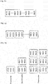
- X-th circuit pattern (1-3) indicates the work procedures for first electronic component 104a to third electronic component 104c scheduled to be mounted on each circuit pattern 102
- X-th circuit pattern (4-6) indicates the work procedures for fourth electronic component 104d to sixth electronic component 104f scheduled to be mounted on each circuit pattern 102
- X-th circuit pattern (6-9) indicates the work procedures for seventh electronic component 104g to ninth electronic component 104i scheduled to be mounted on each circuit pattern 102.
- work procedures of each circuit pattern 102 divided into three groups are distributed between the three mounters 16.
- work procedures from each circuit pattern 102 are distributed between mounters 16 such that mounting positions of electronic components 104 are shared.
- the work procedures for first electronic component 104a to third electronic component 104c scheduled to be mounted on each circuit pattern 102 are set to first mounter 16a
- the work procedures for fourth electronic component 104d to sixth electronic component 104f scheduled to be mounted on each circuit pattern 102 are set to second mounter 16b
- the work procedures for seventh electronic component 104g to ninth electronic component 104i scheduled to be mounted on each circuit pattern 102 are set to third mounter 16c.
- first mounter 16a performs mounting work for first electronic component 104a to third electronic component 104c for first circuit pattern 102a and third circuit pattern 104c without performing mounting work for first electronic component 104a to third electronic component 104c for second circuit pattern 102b.
- second mounter 16b performs mounting work for fourth electronic component 104d to sixth electronic component 104f for first circuit pattern 102a and third circuit pattern 104c without performing mounting work for fourth electronic component 104d to sixth electronic component 104f for second circuit pattern 102b.
- third mounter 16b performs mounting work for seventh electronic component 104g to ninth electronic component 104i for first circuit pattern 102a and third circuit pattern 104c without performing mounting work for seventh electronic component 104g to ninth electronic component 104i for second circuit pattern 102b. That is, at each mounter 16, mounting work is performed for first circuit pattern 102a and third circuit pattern 102c, and mounting work is not performed for second circuit pattern 102b.
- the tact time of substrate work system 10 is reduced by the work time required for second circuit pattern 102b.
- work procedures are set such that mounting work of mounting multiple electronic components 104 for each circuit pattern 102 is performed by all mounters 16, thereby improving throughput in cases in which there is a defective circuit pattern on a multiple-board substrate 100.
- circuit pattern information information related to mounting positions of electronic components to be mounted according to the work procedures
- circuit pattern information information related to circuit pattern 102 that is the target for mounting work according to the work procedures
- R1-9 (1-3) in the figure represents a combination of extracted reference information and circuit pattern information.
- R1 ⁇ 9 represents reference information; for example, R1 represents the electronic component to be mounted according to the work procedures that is first electronic component 104a, and the position at which first electronic component 104a is to be mounted.
- (1-3) represents circuit pattern information; for example, (1) represents first circuit pattern 102a that is the target for mounting work according to the work procedures.
- R1(1) represents the work procedure for mounting an electronic component at the mounting position for first electronic component 104a of first circuit pattern 102a.
- each of the nine groups of reference information is allocated to the three mounters 16.
- each of the nine groups of reference information should be distributed equally between the mounters 16. That is, three groups each should be distributed to each mounter 16.
- each of the nine groups of reference information should be distributed between the three mounters 16 based on the mounting performance of the mounters 16.
- first mounter 16a that is, the quantity of electronic components that can be mounted per unit of time is A components per second
- second mounter 16b is 2A components per second
- third mounter 16c is 6A components per second
- the nine groups are distributed between the three mounters 16 with a ratio of 1:2:6.
- the work procedures for first electronic component 104a scheduled to be mounted on each circuit pattern 102 are set to first mounter 16a
- the work procedures for second electronic component 104b and third electronic component 104c scheduled to be mounted on each circuit pattern 102 are set to second mounter 16b
- the work procedures for fourth electronic component 104d to ninth electronic component 104i scheduled to be mounted on each circuit pattern 102 are set to third mounter 16c.
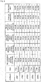
- the applicant calculated the time required to manufacture one multiple-board substrate (hereinafter sometimes referred to as "work time") via simulation.
- Shown in fig. 9 are the work times in a case when setting work procedures according to a conventional method, that is, as shown in fig. 4 , when setting work procedures such that mounting work of one circuit pattern 102 is performed by one mounter 16.
- Shown in fig. 10 are the work times in a case when setting work procedures according to a method used by substrate work system 10, that is, as shown in figs. 6 and 8 , when setting work procedures such that mounting work of each circuit pattern 102 is performed by all the mounters 16.
- work times are displayed for mounting work for five different types of electronic component mounting (JOB1 to JOB5), with the work times displayed for each of the top surfaces (Top) and bottom surfaces (Bottom).
- the "No defective circuit patterns” column shows the work time in a case in which all three circuit patterns 102 on multiple-board substrate 100 are of good condition.
- the "X-th circuit pattern defective” columns show the work time in a case in which the X-th circuit pattern of the three circuit patterns 102 on multiple-board substrate 100 is defective.
- the "Average” column shows the average value of the work times for cases in which there is a defective circuit pattern.
- the "Reduction ratio” shows the reduction ratio of the work time when there is a defective circuit pattern.
- Reduction ratio A ⁇ ("work time when there is no defective circuit pattern" - "average work time when there is a defective circuit pattern") / "work time when there is no defective circuit pattern" ⁇ x 100
- optimization program 110 memorized in controller 92.
- optimization program 110 has setting means 112 that functions as a section for performing setting of work procedures for each mounter 16.
- substrate work system 10 is an example of a substrate work system.
- Mounter 16 is an example of a mounting work machine.
- Control device 90 is an example of a control device.
- Multiple-board substrate 100 is an example of a multiple-board printed panel.
- Circuit pattern 102 is an example of an electronic circuit board pattern.
- Optimization program 110 is an example of an optimization program.
- Setting means 112 is an example of a setting means.
- optimization program 110 is provided in control device 90 that controls operations of substrate work system 10 and control device 90 performs setting of work procedures, however, optimization program 110 may be provided in a device different to control device 90, and setting of work procedures may be performed by the different device.
- 10 substrate work system (mounting work system); 16: mounter (mounting work machine); 90: control device (memory device); 100: multiple-board substrate (multiple-board printed panel); 102: circuit pattern (electronic circuit board pattern); 110: optimization program; 112: setting means
Landscapes
- Engineering & Computer Science (AREA)
- Manufacturing & Machinery (AREA)
- Microelectronics & Electronic Packaging (AREA)
- Operations Research (AREA)
- Supply And Installment Of Electrical Components (AREA)
Applications Claiming Priority (1)
| Application Number | Priority Date | Filing Date | Title |
|---|---|---|---|
| PCT/JP2014/061556 WO2015162751A1 (ja) | 2014-04-24 | 2014-04-24 | 最適化プログラム、および装着作業システム |
Publications (3)
| Publication Number | Publication Date |
|---|---|
| EP3136833A1 true EP3136833A1 (de) | 2017-03-01 |
| EP3136833A4 EP3136833A4 (de) | 2017-05-17 |
| EP3136833B1 EP3136833B1 (de) | 2018-11-28 |
Family
ID=54331938
Family Applications (1)
| Application Number | Title | Priority Date | Filing Date |
|---|---|---|---|
| EP14890427.9A Active EP3136833B1 (de) | 2014-04-24 | 2014-04-24 | Optimierungsprogramm und montageoperationssystem |
Country Status (5)
| Country | Link |
|---|---|
| US (1) | US10729048B2 (de) |
| EP (1) | EP3136833B1 (de) |
| JP (1) | JP6691039B2 (de) |
| CN (1) | CN106233830B (de) |
| WO (1) | WO2015162751A1 (de) |
Families Citing this family (2)
| Publication number | Priority date | Publication date | Assignee | Title |
|---|---|---|---|---|
| CN112789959B (zh) * | 2018-10-02 | 2022-08-19 | 株式会社富士 | 作业机 |
| CN116160210B (zh) * | 2022-12-09 | 2026-02-17 | 阳光新能源开发股份有限公司 | 光伏组件安装方法和光伏组件安装系统 |
Family Cites Families (11)
| Publication number | Priority date | Publication date | Assignee | Title |
|---|---|---|---|---|
| JP3474682B2 (ja) | 1995-08-07 | 2003-12-08 | 松下電器産業株式会社 | 実装部品振り分け方法及び実装設備 |
| DE60039547D1 (de) | 1999-09-27 | 2008-08-28 | Matsushita Electric Industrial Co Ltd | Bestückungsverfahren und Bestückungsvorrichtung |
| JP4004702B2 (ja) | 2000-02-24 | 2007-11-07 | 松下電器産業株式会社 | 電子部品実装方法 |
| JP2005072317A (ja) | 2003-08-26 | 2005-03-17 | Matsushita Electric Ind Co Ltd | 実装方法及び装置 |
| KR101062511B1 (ko) | 2003-09-01 | 2011-09-06 | 파나소닉 주식회사 | 부품 장착 순서의 최적화 방법 및 부품 장착 순서의 최적화장치 |
| US20050072317A1 (en) * | 2003-10-02 | 2005-04-07 | Thorstad Richard D. | Device for forming piecrust blanks |
| JP2006339388A (ja) * | 2005-06-01 | 2006-12-14 | Yamaha Motor Co Ltd | 実装作業の管理方法、実装ラインおよび実装機 |
| JP4884349B2 (ja) | 2007-10-19 | 2012-02-29 | 富士機械製造株式会社 | 部品実装方法及び部品実装制御装置 |
| JP5459852B2 (ja) * | 2010-04-02 | 2014-04-02 | 富士機械製造株式会社 | 多数個取り基板の電子部品実装方法 |
| JP5190127B2 (ja) | 2011-02-02 | 2013-04-24 | ヤマハ発動機株式会社 | 基板処理装置 |
| WO2014030255A1 (ja) | 2012-08-24 | 2014-02-27 | 富士機械製造株式会社 | 最適化プログラム、および、対基板作業システム |
-
2014
- 2014-04-24 JP JP2016514636A patent/JP6691039B2/ja active Active
- 2014-04-24 WO PCT/JP2014/061556 patent/WO2015162751A1/ja not_active Ceased
- 2014-04-24 US US15/305,174 patent/US10729048B2/en active Active
- 2014-04-24 CN CN201480078091.9A patent/CN106233830B/zh active Active
- 2014-04-24 EP EP14890427.9A patent/EP3136833B1/de active Active
Also Published As
| Publication number | Publication date |
|---|---|
| US10729048B2 (en) | 2020-07-28 |
| CN106233830A (zh) | 2016-12-14 |
| US20170042072A1 (en) | 2017-02-09 |
| EP3136833A4 (de) | 2017-05-17 |
| CN106233830B (zh) | 2019-03-05 |
| JP6691039B2 (ja) | 2020-04-28 |
| EP3136833B1 (de) | 2018-11-28 |
| WO2015162751A1 (ja) | 2015-10-29 |
| JPWO2015162751A1 (ja) | 2017-04-13 |
Similar Documents
| Publication | Publication Date | Title |
|---|---|---|
| JP6109178B2 (ja) | 最適化プログラム、および、対基板作業システム | |
| CN106879246A (zh) | 电子部件安装装置、电子部件安装系统及安装方法 | |
| EP3016490B1 (de) | Komponentenmontagemaschine | |
| US10345792B2 (en) | Group determination method and group determination apparatus | |
| EP3136833B1 (de) | Optimierungsprogramm und montageoperationssystem | |
| EP2961253A1 (de) | Komponentenmontagesystem und schüttgutkomponentenbestimmungsverfahren dafür | |
| JP6405317B2 (ja) | サーボコントローラ | |
| US10820460B2 (en) | Cutting and bending device | |
| US10701850B2 (en) | Optimization program and mounting machine | |
| US11586169B2 (en) | Production management device | |
| US20170127582A1 (en) | Electronic component mounting method and electronic component mounting system | |
| US20170325371A1 (en) | Control device of electronic component mounting machine and data input device for control device thereof | |
| JP2010010272A (ja) | 部品実装装置および部品実装方法 | |
| JPWO2016174715A1 (ja) | 作業機 | |
| US11153999B2 (en) | Work machine | |
| JP2013084862A (ja) | 電子部品実装装置 | |
| JP5792586B2 (ja) | 電子部品実装システム、電子部品実装方法及び電子部品実装用コンピュータプログラム | |
| JP7805881B2 (ja) | 部品実装システム | |
| WO2024116222A1 (ja) | プログラム作成装置 | |
| WO2024201742A1 (ja) | 基板生産計画装置、基板生産計画方法および基板生産計画プログラム | |
| JP6691559B2 (ja) | 対基板作業装置 | |
| CN117561803A (zh) | 生产程序生成方法 |
Legal Events
| Date | Code | Title | Description |
|---|---|---|---|
| STAA | Information on the status of an ep patent application or granted ep patent |
Free format text: STATUS: THE INTERNATIONAL PUBLICATION HAS BEEN MADE |
|
| PUAI | Public reference made under article 153(3) epc to a published international application that has entered the european phase |
Free format text: ORIGINAL CODE: 0009012 |
|
| STAA | Information on the status of an ep patent application or granted ep patent |
Free format text: STATUS: REQUEST FOR EXAMINATION WAS MADE |
|
| 17P | Request for examination filed |
Effective date: 20161021 |
|
| AK | Designated contracting states |
Kind code of ref document: A1 Designated state(s): AL AT BE BG CH CY CZ DE DK EE ES FI FR GB GR HR HU IE IS IT LI LT LU LV MC MK MT NL NO PL PT RO RS SE SI SK SM TR |
|
| AX | Request for extension of the european patent |
Extension state: BA ME |
|
| A4 | Supplementary search report drawn up and despatched |
Effective date: 20170419 |
|
| RIC1 | Information provided on ipc code assigned before grant |
Ipc: H05K 13/04 20060101AFI20170411BHEP Ipc: H05K 13/08 20060101ALI20170411BHEP |
|
| DAX | Request for extension of the european patent (deleted) | ||
| GRAP | Despatch of communication of intention to grant a patent |
Free format text: ORIGINAL CODE: EPIDOSNIGR1 |
|
| STAA | Information on the status of an ep patent application or granted ep patent |
Free format text: STATUS: GRANT OF PATENT IS INTENDED |
|
| INTG | Intention to grant announced |
Effective date: 20180719 |
|
| RIN1 | Information on inventor provided before grant (corrected) |
Inventor name: YASUI, YOSHIHIRO |
|
| GRAS | Grant fee paid |
Free format text: ORIGINAL CODE: EPIDOSNIGR3 |
|
| RAP1 | Party data changed (applicant data changed or rights of an application transferred) |
Owner name: FUJI CORPORATION |
|
| GRAA | (expected) grant |
Free format text: ORIGINAL CODE: 0009210 |
|
| STAA | Information on the status of an ep patent application or granted ep patent |
Free format text: STATUS: THE PATENT HAS BEEN GRANTED |
|
| AK | Designated contracting states |
Kind code of ref document: B1 Designated state(s): AL AT BE BG CH CY CZ DE DK EE ES FI FR GB GR HR HU IE IS IT LI LT LU LV MC MK MT NL NO PL PT RO RS SE SI SK SM TR |
|
| REG | Reference to a national code |
Ref country code: CH Ref legal event code: EP |
|
| REG | Reference to a national code |
Ref country code: DE Ref legal event code: R096 Ref document number: 602014037211 Country of ref document: DE |
|
| REG | Reference to a national code |
Ref country code: AT Ref legal event code: REF Ref document number: 1071852 Country of ref document: AT Kind code of ref document: T Effective date: 20181215 |
|
| REG | Reference to a national code |
Ref country code: IE Ref legal event code: FG4D |
|
| REG | Reference to a national code |
Ref country code: CH Ref legal event code: PK Free format text: BERICHTIGUNGEN |
|
| RIN2 | Information on inventor provided after grant (corrected) |
Inventor name: YASUI, YOSHIHIRO |
|
| REG | Reference to a national code |
Ref country code: NL Ref legal event code: MP Effective date: 20181128 |
|
| REG | Reference to a national code |
Ref country code: LT Ref legal event code: MG4D |
|
| REG | Reference to a national code |
Ref country code: AT Ref legal event code: MK05 Ref document number: 1071852 Country of ref document: AT Kind code of ref document: T Effective date: 20181128 |
|
| PG25 | Lapsed in a contracting state [announced via postgrant information from national office to epo] |
Ref country code: ES Free format text: LAPSE BECAUSE OF FAILURE TO SUBMIT A TRANSLATION OF THE DESCRIPTION OR TO PAY THE FEE WITHIN THE PRESCRIBED TIME-LIMIT Effective date: 20181128 Ref country code: AT Free format text: LAPSE BECAUSE OF FAILURE TO SUBMIT A TRANSLATION OF THE DESCRIPTION OR TO PAY THE FEE WITHIN THE PRESCRIBED TIME-LIMIT Effective date: 20181128 Ref country code: LV Free format text: LAPSE BECAUSE OF FAILURE TO SUBMIT A TRANSLATION OF THE DESCRIPTION OR TO PAY THE FEE WITHIN THE PRESCRIBED TIME-LIMIT Effective date: 20181128 Ref country code: IS Free format text: LAPSE BECAUSE OF FAILURE TO SUBMIT A TRANSLATION OF THE DESCRIPTION OR TO PAY THE FEE WITHIN THE PRESCRIBED TIME-LIMIT Effective date: 20190328 Ref country code: FI Free format text: LAPSE BECAUSE OF FAILURE TO SUBMIT A TRANSLATION OF THE DESCRIPTION OR TO PAY THE FEE WITHIN THE PRESCRIBED TIME-LIMIT Effective date: 20181128 Ref country code: NO Free format text: LAPSE BECAUSE OF FAILURE TO SUBMIT A TRANSLATION OF THE DESCRIPTION OR TO PAY THE FEE WITHIN THE PRESCRIBED TIME-LIMIT Effective date: 20190228 Ref country code: HR Free format text: LAPSE BECAUSE OF FAILURE TO SUBMIT A TRANSLATION OF THE DESCRIPTION OR TO PAY THE FEE WITHIN THE PRESCRIBED TIME-LIMIT Effective date: 20181128 Ref country code: BG Free format text: LAPSE BECAUSE OF FAILURE TO SUBMIT A TRANSLATION OF THE DESCRIPTION OR TO PAY THE FEE WITHIN THE PRESCRIBED TIME-LIMIT Effective date: 20190228 Ref country code: LT Free format text: LAPSE BECAUSE OF FAILURE TO SUBMIT A TRANSLATION OF THE DESCRIPTION OR TO PAY THE FEE WITHIN THE PRESCRIBED TIME-LIMIT Effective date: 20181128 |
|
| PG25 | Lapsed in a contracting state [announced via postgrant information from national office to epo] |
Ref country code: RS Free format text: LAPSE BECAUSE OF FAILURE TO SUBMIT A TRANSLATION OF THE DESCRIPTION OR TO PAY THE FEE WITHIN THE PRESCRIBED TIME-LIMIT Effective date: 20181128 Ref country code: SE Free format text: LAPSE BECAUSE OF FAILURE TO SUBMIT A TRANSLATION OF THE DESCRIPTION OR TO PAY THE FEE WITHIN THE PRESCRIBED TIME-LIMIT Effective date: 20181128 Ref country code: GR Free format text: LAPSE BECAUSE OF FAILURE TO SUBMIT A TRANSLATION OF THE DESCRIPTION OR TO PAY THE FEE WITHIN THE PRESCRIBED TIME-LIMIT Effective date: 20190301 Ref country code: PT Free format text: LAPSE BECAUSE OF FAILURE TO SUBMIT A TRANSLATION OF THE DESCRIPTION OR TO PAY THE FEE WITHIN THE PRESCRIBED TIME-LIMIT Effective date: 20190328 Ref country code: AL Free format text: LAPSE BECAUSE OF FAILURE TO SUBMIT A TRANSLATION OF THE DESCRIPTION OR TO PAY THE FEE WITHIN THE PRESCRIBED TIME-LIMIT Effective date: 20181128 |
|
| PG25 | Lapsed in a contracting state [announced via postgrant information from national office to epo] |
Ref country code: NL Free format text: LAPSE BECAUSE OF FAILURE TO SUBMIT A TRANSLATION OF THE DESCRIPTION OR TO PAY THE FEE WITHIN THE PRESCRIBED TIME-LIMIT Effective date: 20181128 |
|
| PG25 | Lapsed in a contracting state [announced via postgrant information from national office to epo] |
Ref country code: CZ Free format text: LAPSE BECAUSE OF FAILURE TO SUBMIT A TRANSLATION OF THE DESCRIPTION OR TO PAY THE FEE WITHIN THE PRESCRIBED TIME-LIMIT Effective date: 20181128 Ref country code: PL Free format text: LAPSE BECAUSE OF FAILURE TO SUBMIT A TRANSLATION OF THE DESCRIPTION OR TO PAY THE FEE WITHIN THE PRESCRIBED TIME-LIMIT Effective date: 20181128 Ref country code: IT Free format text: LAPSE BECAUSE OF FAILURE TO SUBMIT A TRANSLATION OF THE DESCRIPTION OR TO PAY THE FEE WITHIN THE PRESCRIBED TIME-LIMIT Effective date: 20181128 Ref country code: DK Free format text: LAPSE BECAUSE OF FAILURE TO SUBMIT A TRANSLATION OF THE DESCRIPTION OR TO PAY THE FEE WITHIN THE PRESCRIBED TIME-LIMIT Effective date: 20181128 |
|
| REG | Reference to a national code |
Ref country code: DE Ref legal event code: R097 Ref document number: 602014037211 Country of ref document: DE |
|
| PG25 | Lapsed in a contracting state [announced via postgrant information from national office to epo] |
Ref country code: RO Free format text: LAPSE BECAUSE OF FAILURE TO SUBMIT A TRANSLATION OF THE DESCRIPTION OR TO PAY THE FEE WITHIN THE PRESCRIBED TIME-LIMIT Effective date: 20181128 Ref country code: SK Free format text: LAPSE BECAUSE OF FAILURE TO SUBMIT A TRANSLATION OF THE DESCRIPTION OR TO PAY THE FEE WITHIN THE PRESCRIBED TIME-LIMIT Effective date: 20181128 Ref country code: SM Free format text: LAPSE BECAUSE OF FAILURE TO SUBMIT A TRANSLATION OF THE DESCRIPTION OR TO PAY THE FEE WITHIN THE PRESCRIBED TIME-LIMIT Effective date: 20181128 Ref country code: EE Free format text: LAPSE BECAUSE OF FAILURE TO SUBMIT A TRANSLATION OF THE DESCRIPTION OR TO PAY THE FEE WITHIN THE PRESCRIBED TIME-LIMIT Effective date: 20181128 |
|
| PLBE | No opposition filed within time limit |
Free format text: ORIGINAL CODE: 0009261 |
|
| STAA | Information on the status of an ep patent application or granted ep patent |
Free format text: STATUS: NO OPPOSITION FILED WITHIN TIME LIMIT |
|
| PG25 | Lapsed in a contracting state [announced via postgrant information from national office to epo] |
Ref country code: SI Free format text: LAPSE BECAUSE OF FAILURE TO SUBMIT A TRANSLATION OF THE DESCRIPTION OR TO PAY THE FEE WITHIN THE PRESCRIBED TIME-LIMIT Effective date: 20181128 |
|
| 26N | No opposition filed |
Effective date: 20190829 |
|
| REG | Reference to a national code |
Ref country code: CH Ref legal event code: PL |
|
| REG | Reference to a national code |
Ref country code: BE Ref legal event code: MM Effective date: 20190430 |
|
| GBPC | Gb: european patent ceased through non-payment of renewal fee |
Effective date: 20190424 |
|
| PG25 | Lapsed in a contracting state [announced via postgrant information from national office to epo] |
Ref country code: MC Free format text: LAPSE BECAUSE OF FAILURE TO SUBMIT A TRANSLATION OF THE DESCRIPTION OR TO PAY THE FEE WITHIN THE PRESCRIBED TIME-LIMIT Effective date: 20181128 Ref country code: LU Free format text: LAPSE BECAUSE OF NON-PAYMENT OF DUE FEES Effective date: 20190424 |
|
| PG25 | Lapsed in a contracting state [announced via postgrant information from national office to epo] |
Ref country code: CH Free format text: LAPSE BECAUSE OF NON-PAYMENT OF DUE FEES Effective date: 20190430 Ref country code: GB Free format text: LAPSE BECAUSE OF NON-PAYMENT OF DUE FEES Effective date: 20190424 Ref country code: LI Free format text: LAPSE BECAUSE OF NON-PAYMENT OF DUE FEES Effective date: 20190430 |
|
| PG25 | Lapsed in a contracting state [announced via postgrant information from national office to epo] |
Ref country code: BE Free format text: LAPSE BECAUSE OF NON-PAYMENT OF DUE FEES Effective date: 20190430 Ref country code: FR Free format text: LAPSE BECAUSE OF NON-PAYMENT OF DUE FEES Effective date: 20190430 |
|
| PG25 | Lapsed in a contracting state [announced via postgrant information from national office to epo] |
Ref country code: TR Free format text: LAPSE BECAUSE OF FAILURE TO SUBMIT A TRANSLATION OF THE DESCRIPTION OR TO PAY THE FEE WITHIN THE PRESCRIBED TIME-LIMIT Effective date: 20181128 |
|
| PG25 | Lapsed in a contracting state [announced via postgrant information from national office to epo] |
Ref country code: IE Free format text: LAPSE BECAUSE OF NON-PAYMENT OF DUE FEES Effective date: 20190424 |
|
| PG25 | Lapsed in a contracting state [announced via postgrant information from national office to epo] |
Ref country code: CY Free format text: LAPSE BECAUSE OF FAILURE TO SUBMIT A TRANSLATION OF THE DESCRIPTION OR TO PAY THE FEE WITHIN THE PRESCRIBED TIME-LIMIT Effective date: 20181128 |
|
| PG25 | Lapsed in a contracting state [announced via postgrant information from national office to epo] |
Ref country code: HU Free format text: LAPSE BECAUSE OF FAILURE TO SUBMIT A TRANSLATION OF THE DESCRIPTION OR TO PAY THE FEE WITHIN THE PRESCRIBED TIME-LIMIT; INVALID AB INITIO Effective date: 20140424 Ref country code: MT Free format text: LAPSE BECAUSE OF FAILURE TO SUBMIT A TRANSLATION OF THE DESCRIPTION OR TO PAY THE FEE WITHIN THE PRESCRIBED TIME-LIMIT Effective date: 20181128 |
|
| PG25 | Lapsed in a contracting state [announced via postgrant information from national office to epo] |
Ref country code: MK Free format text: LAPSE BECAUSE OF FAILURE TO SUBMIT A TRANSLATION OF THE DESCRIPTION OR TO PAY THE FEE WITHIN THE PRESCRIBED TIME-LIMIT Effective date: 20181128 |
|
| P01 | Opt-out of the competence of the unified patent court (upc) registered |
Effective date: 20230328 |
|
| PGFP | Annual fee paid to national office [announced via postgrant information from national office to epo] |
Ref country code: DE Payment date: 20250305 Year of fee payment: 12 |