EP3134743B1 - Integrierte schaltung und zugehöriges verfahren zur messung einer externen impedanz - Google Patents
Integrierte schaltung und zugehöriges verfahren zur messung einer externen impedanz Download PDFInfo
- Publication number
- EP3134743B1 EP3134743B1 EP15727208.9A EP15727208A EP3134743B1 EP 3134743 B1 EP3134743 B1 EP 3134743B1 EP 15727208 A EP15727208 A EP 15727208A EP 3134743 B1 EP3134743 B1 EP 3134743B1
- Authority
- EP
- European Patent Office
- Prior art keywords
- integrated circuit
- output
- circuit
- power supply
- oscillation
- Prior art date
- Legal status (The legal status is an assumption and is not a legal conclusion. Google has not performed a legal analysis and makes no representation as to the accuracy of the status listed.)
- Active
Links
Images

Classifications
-
- G—PHYSICS
- G01—MEASURING; TESTING
- G01R—MEASURING ELECTRIC VARIABLES; MEASURING MAGNETIC VARIABLES
- G01R27/00—Arrangements for measuring resistance, reactance, impedance, or electric characteristics derived therefrom
- G01R27/02—Measuring real or complex resistance, reactance, impedance, or other two-pole characteristics derived therefrom, e.g. time constant
- G01R27/20—Measuring earth resistance; Measuring contact resistance, e.g. of earth connections, e.g. plates
- G01R27/205—Measuring contact resistance of connections, e.g. of earth connections
-
- G—PHYSICS
- G01—MEASURING; TESTING
- G01R—MEASURING ELECTRIC VARIABLES; MEASURING MAGNETIC VARIABLES
- G01R31/00—Arrangements for testing electric properties; Arrangements for locating electric faults; Arrangements for electrical testing characterised by what is being tested not provided for elsewhere
- G01R31/28—Testing of electronic circuits, e.g. by signal tracer
- G01R31/2851—Testing of integrated circuits [IC]
- G01R31/2853—Electrical testing of internal connections or -isolation, e.g. latch-up or chip-to-lead connections
-
- G—PHYSICS
- G01—MEASURING; TESTING
- G01R—MEASURING ELECTRIC VARIABLES; MEASURING MAGNETIC VARIABLES
- G01R31/00—Arrangements for testing electric properties; Arrangements for locating electric faults; Arrangements for electrical testing characterised by what is being tested not provided for elsewhere
- G01R31/28—Testing of electronic circuits, e.g. by signal tracer
- G01R31/2851—Testing of integrated circuits [IC]
- G01R31/2855—Environmental, reliability or burn-in testing
- G01R31/2856—Internal circuit aspects, e.g. built-in test features; Test chips; Measuring material aspects, e.g. electro migration [EM]
Definitions
- This disclosure relates generally to integrated circuits, and, more particularly, to an integrated circuit and associated methods capable of determining an external impedance associated with the integrated circuit.
- Integrated circuit performance is affected not only by internal factors, such as tolerances associated with semiconductor fabrication techniques, but is likewise influenced by external factors, such as the impedance associated with external circuits and connections.
- the impedance sometimes referred to as "contact resistance" associated with a connection of the integrated circuit to an external device, such as a power supply of Automatic Test Equipment (ATE), can significantly affect the integrated circuit performance. Elevated contact resistance can indicate a complete failure of a particular integrated circuit connection (i.e., a broken lead wire or solder connection) and even less significantly elevated contact resistance can degrade integrated circuit performance.
- some integrated circuit functions require a minimum supply voltage and a high contact resistance can result in an insufficient supply voltage level at the integrated circuit for certain circuit functionality.
- One technique for measuring external impedance in a test environment is a manual process whereby a supply voltage coupled to the integrated circuit is set at a first level while the current and voltage at a particular IC connection is measured, such as with a Kelvin connection. The supply voltage is thereafter set to a second level while the current and voltage at the same connection is measured and the ratio of the difference between the voltages and currents measured at the two supply voltage levels is computed to provide an indication of the contact resistance.
- this technique for measuring external impedance tends to be slow and labor intensive and therefore costly to the overall IC manufacturing process.
- WO 2007/093172 A2 discloses an integrated circuit arrangement having at least one electronic component, and also at least one resistance determining circuit that is coupled to the electronic component and is monolithically integrated with the latter and serves for determining the parasitic non-reactive resistance of at least the lead to the at least one electronic component.
- US 2007/080697 A1 discloses a contact resistance measuring circuit configured to determine the contact resistance of a testing device.
- the measuring circuit is coupled to a processing circuit and the testing device, and includes a pair of input/output units coupled together via a pass device.
- Each of the input/output units includes a pull-up device and a pull-down device to provide separate pull-up and pull-down control, respectively.
- the pull-up devices, the pull-down devices, and the pass device are dynamically configurable such that the measuring circuit uses either a pull-up mode or a pull-down mode to measure voltage and current characteristics of each contact point, or pin, of the testing device.
- the processing circuit calculates the contact resistance for each pin according to the measured voltage and current characteristics. The calculated contact resistances are used to calibrate the testing device.
- EP 0352734 A1 relates to circuitry for monitoring a voltage source relative to two reference voltages; US 3679916 A relates to a controlled hysteresis integrated circuit switching circuit; and US 2013/027089 A1 relates to a circuit and method for detecting multiple supply voltages.
- the present disclosure provides an integrated circuit with built-in impedance measurement circuitry according to claim 1 and associated methods according to claim 11 capable of determining an external impedance associated with the integrated circuit without the use of time and labor intensive techniques or specialized impedance measurement instruments. Furthermore the described circuitry and methods can be used when the integrated circuit is in use in its intended application as opposed to only during the manufacturing and testing process.
- an integrated circuit in one aspect, includes an output circuit having a first terminal adapted to couple to an external power supply, a second terminal adapted to couple to a reference potential, and a third, control terminal. The first and second terminals provide output terminals of the integrated circuit. Additionally, the integrated circuit includes an impedance measurement circuit responsive to the external power supply to generate a control signal for coupling to the control terminal of the output circuit. The control signal controls a current level associated with the output circuit.
- the impedance measurement circuit may include a resistor divider coupled between the power supply and the reference potential and a comparator responsive to a voltage associated with the resistor divider, wherein an output signal of the comparator provides the control signal.
- the impedance measurement circuit may include a logic gate coupled to receive the output signal of the comparator and a test mode signal to provide the control signal.
- the impedance measurement circuit may include a resistor divider coupled between the power supply and the reference potential and a voltage associated with the resistor divider may provide the control signal.
- An oscillation of an output signal of the integrated circuit is indicative of an external impedance associated with the integrated circuit.
- a time of occurrence of the oscillation and/or a duration of the oscillation is indicative of the external impedance.
- the integrated circuit further may include one or more of the following:
- the comparator may have hysteresis.
- the monitored output signal may be a current provided by the output circuit.
- the external power supply may provide a supply voltage that is ramped through a predetermined voltage range at a predetermined rate. A transition in the control signal may cause an increase in the current level of the output circuit.
- the output circuit may include a current source, the integrated circuit may be a magnetic field sensor and/or the external power supply may be associated with an ATE system.
- a method for determining an external impedance associated with an integrated circuit includes coupling an external power supply to the integrated circuit, the integrated circuit having an output circuit with a first terminal adapted to couple to the external power supply, a second terminal adapted to couple to a reference potential, and a third, control terminal.
- the first and second terminals provide output terminals of the integrated circuit.
- a control signal for coupling to the control terminal of the output circuit is generated in response to a supply voltage from the external power supply.
- the method also includes ramping the supply voltage of the external power supply through a predetermined range of voltages and controlling a current level associated with the output circuit in response to the control signal.
- An output signal of the integrated circuit is monitored for an oscillation and the external impedance is determined in response to the oscillation.
- Generating the control signal may include level shifting the supply voltage and/or comparing a level shifted version of the supply voltage to a threshold voltage.
- the output circuit includes a current source and monitoring the output signal for an oscillation includes monitoring a current level of the current source.
- the external impedance is determined in response to a time of occurrence of the oscillation, a duration of the oscillation, or both.
- the integrated circuit may be a magnetic field sensor and/or the external power supply may be associated with an ATE system.
- magnetic field sensor is used to describe a circuit that uses a magnetic field sensing element, generally in combination with other circuits.
- Magnetic field sensors are used in a variety of applications, including, but not limited to, an angle sensor that senses an angle of a direction of a magnetic field, a current sensor that senses a magnetic field generated by a current carried by a current-carrying conductor, a magnetic switch that senses the proximity of a ferromagnetic object, a rotation detector that senses passing ferromagnetic articles, for example, magnetic domains of a ring magnet or a ferromagnetic target (e.g., gear teeth) where the magnetic field sensor is used in combination with a back-biased or other magnet, and a magnetic field sensor that senses a magnetic field density of a magnetic field.
- an angle sensor that senses an angle of a direction of a magnetic field
- a current sensor that senses a magnetic field generated by a current carried by a current-carrying conductor
- a magnetic switch that
- magnetic field sensing element is used to describe a variety of electronic elements that can sense a magnetic field.
- the magnetic field sensing element can be, but is not limited to, a Hall effect element, a magnetoresistance element, or a magnetotransistor.
- Hall effect elements for example, a planar Hall element, a vertical Hall element, and a Circular Vertical Hall (CVH) element.
- magnetoresistance elements for example, a semiconductor magnetoresistance element such as Indium Antimonide (InSb), a giant magnetoresistance (GMR) element, for example, a spin valve, an anisotropic magnetoresistance element (AMR), a tunneling magnetoresistance (TMR) element, and a magnetic tunnel junction (MTJ).
- the magnetic field sensing element may be a single element or, alternatively, may include two or more magnetic field sensing elements arranged in various configurations, e.g., a half bridge or full (Wheatstone) bridge.
- the magnetic field sensing element may be a device made of a type IV semiconductor material such as Silicon (Si) or Germanium (Ge), or a type III-V semiconductor material like Gallium-Arsenide (GaAs) or an Indium compound, e.g., Indium-Antimonide (InSb).
- a type IV semiconductor material such as Silicon (Si) or Germanium (Ge)
- a type III-V semiconductor material like Gallium-Arsenide (GaAs) or an Indium compound, e.g., Indium-Antimonide (InSb).
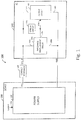
- the system 100 includes integrated circuit 140 adapted to couple to a device 110 having a power supply 120. More particularly, the integrated circuit 140 includes an output circuit 160 having a first terminal 160a adapted to couple to the power supply 120, a second terminal 160b adapted to couple to a reference potential (e.g., GND), and a third, control terminal 160c.
- a reference potential e.g., GND
- the integrated circuit 140 additionally includes an impedance measurement circuit 150 having a first terminal 150a adapted to couple to the power supply 120, a second terminal 150b adapted to couple to the reference potential, and a third terminal 150c adapted to couple to the control terminal 160c of the output circuit.
- the impedance measurement circuit 150 generates a control signal for coupling to the output circuit 160 to control a current level associated with the output circuit as will be explained.
- the integrated circuit 140 and the device 110 are shown as coupled to a contact resistance 130.
- the contact resistance 130 is, generally, representative of resistance(s) existing between and associated with the integrated circuit 140 and/or the device 110 and their interconnections. More particularly, the contact resistance 130 represents resistance associated with electrical leads of the integrated circuit 140 and/or the device 110, resistance associated with conductive traces on a circuit board associated with the device 110 and/or on the integrated circuit, and other interconnects associated with the integrated circuit 140 and/or the device 110 (such as solder connections, wire, cabling, or other conductor connections), and the like.
- the device 110 may, for example, be an Automatic Test Equipment (ATE) system, with the power supply 120 being representative of a power supply associated with the ATE system.
- the power supply 120 is capable of ramping a supply voltage (VCC) provided by the power supply 120 through a predetermined range of voltages at a predetermined rate and may do so under the control of a control signal provided at a control terminal 120a.
- VCC-IR The supply voltage received by the integrated circuit 140 is represented as VCC-IR, which is representative of the supply voltage (VCC) less a voltage drop (IR) resulting from the contact resistance 130.
- the integrated circuit 140 may take any form of circuit which would benefit from on-chip contact resistance characterization.
- the integrated circuit 140 can be a digital integrated circuit (e.g., microprocessor), linear integrated circuit, or a mixed-signal integrated circuit and representative of a device under test (DUT).
- the integrated circuit 140 can, for example, be coupled to the device 110 (e.g., ATE system) through a load (or interface) board, which may also contribute to the contact resistance 130.
- the integrated circuit 140 is a sensor integrated circuit containing sensor circuitry 170; however, it will be appreciated that the circuitry 170 more generally represents the integrated circuit functionality.
- the integrated circuit 140 may be a magnetic field sensor integrated circuit that contains one or more magnetic field sensing elements as part of the sensor circuitry 170 and that provides an output signal indicative of a magnetic field.
- a magnetic field sensor integrated circuit may be a linear sensor in which case the output circuit 160 may provide an output signal, such as in the form of a current, which is proportional to a sensed magnetic field.
- such a magnetic field sensor integrated circuit may operate as a binary switch to provide an output signal at one of two levels depending on whether the sensed magnetic field is greater or less than a particular threshold.
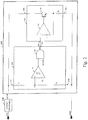
- an integrated circuit 240 which can be the same as or similar to the integrated circuit 140 described above in conjunction with FIG. 1 , is shown coupled to a contact resistance 230, which can be the same as or similar to contact resistance 130 of FIG. 1 , and thus, which is representative of resistance(s) between and associated with the integrated circuit 240 and an external power supply (not shown).
- the external power supply (not shown) may be the same as or similar to the power supply 120 of device 110 shown in FIG. 1 .
- the power supply 120 may, for example, be a power supply of an ATE system.
- the integrated circuit 240 like the integrated circuit 140 of FIG. 1 , can be any type of integrated circuit that would benefit from external impedance characterization.
- the integrated circuit 240 contains circuitry, which may be the same as or similar to the sensor circuitry 170 of FIG. 1 , which represents functionality of the integrated circuit.
- the integrated circuit 240 includes an impedance measurement circuit 250 having a resistor divider, as indicated by R1 and R2, a comparator 252, and a logic gate 254.
- the resistor divider is coupled between a first terminal 250a and a second terminal 250b of the impedance measurement circuit 250.
- the first impedance measurement terminal 250a is adapted to couple to the external power supply (not shown), and the second impedance measurement terminal 250b is adapted to couple to a reference potential (GND).
- the voltage at node R is proportional to the voltage VCC-IR.
- resistors R1 and R2 and the ratio of the values of resistors R1 and R2 can, for example, be chosen based on a voltage level associated with the supply voltage (VCC) and/or the predetermined range of voltages of the supply voltage (VCC) and/or a threshold voltage level V TH .
- the comparator 252 is coupled to receive a voltage associated with the resistor divider (e.g., a voltage potential at node R) at a first comparator input and the threshold voltage (V TH ) at a second comparator input and is configured to generate a comparison signal in response to the first comparator input and the second comparator input.
- the threshold voltage (V TH ) can be selected based on various factors, such as available voltage levels on the integrated circuit, the external supply voltage level (VCC), and/or the level shifting by the resistor divider.
- the threshold voltage (V TH ) can be a fixed voltage, as may be available on the integrated circuit 240 and as may be level shifted by the resistor divider.
- the comparator 252 has hysteresis that is selected based on the minimum contact resistance to be detected, as will be explained below. While various different factors may be considered in selecting the resistor divider, the threshold voltage V TH , and the comparator hysteresis, all of these choices are considered together in order to cause a Cntrl signal (provided by the impedance measurement circuit 250) to transition when the VCC-IR voltage falls below a predetermined level indicative of a contact resistance level equal to or greater than a predetermined contact resistance level to be detected for a given supply voltage level (VCC).
- VCC supply voltage level
- the comparator 252 is coupled to a logic gate 254 that receives the comparison signal at a first logic gate input and a test mode signal (Test Mode) at a second logic gate input and is configured to generate a logic gate output signal (Cntrl) at a third terminal 250c of the impedance measurement circuit 250 in response to the first logic gate input and the second logic gate input.
- the test mode signal can, for example, initiate a test mode operation.
- the integrated circuit 240 is configured to measure an external impedance.
- the integrated circuit 240 is configured to perform its intended function(s) via circuitry, such as circuitry 170 in FIG. 1 (e.g., magnetic field sensing).
- the logic gate 254 is an AND gate.
- the integrated circuit 240 also includes an output circuit 260 having an operational amplifier 262, a transistor 264 and a resistor RO and an associated current level.
- the output circuit 260 is provided in the form of a current source and the associated current level is the level of the current that the current source sinks.
- the output circuit 260 has a first terminal 260a adapted to couple to an external power supply (not shown), a second terminal 260b adapted to couple to a reference potential, and a third, control terminal 260c adapted to couple to the third terminal 250c of the impedance measurement circuit 250 at which the logic gate output signal is provided and which, in the illustrated embodiment, provides the control signal (Cntrl) to the output circuit 260.
- the first and second terminals 260a, 260b of the output circuit provide output terminals of the integrated circuit 240.
- the integrated circuit output is a current provided by the current source between terminals 260a, 260b.
- the operational amplifier 262 is coupled to receive the control signal (Cntrl) from the third terminal 250c of the impedance measurement circuit 250 at its non-inverting input and provides an output signal to a control terminal of transistor 264.
- the transistor is an bipolar npn device having a first terminal (e.g., collector terminal) adapted to couple to the first terminal 260a of the output circuit 260, a second terminal (e.g., emitter terminal) adapted to couple to the inverting input of the operational amplifier 262 and to the resistor RO, and a third terminal (e.g., base terminal) adapted to couple to the operational amplifier output.
- the comparison signal at the output of the comparator provides the control signal (Cntrl) to the third, control terminal 260c of the output circuit and the logic gate 254 is eliminated.
- a voltage associated with the resistor divider (e.g., at node R) of the impedance measurement circuit 250 provides the control signal (Cntrl) to the third, control terminal 260c of the output circuit 260 and the comparator 252 is eliminated.
- the external power supply (not shown) is configured to ramp the supply voltage (VCC) through a predetermined range of voltages.
- the supply voltage is ramped from a first voltage of the predetermined range of voltages to a second lower voltage of the predetermined range of voltages.
- the first voltage is lower than the second voltage.
- the predetermined range of voltages can, for example, be selected based on the specified supply voltage range of the integrated circuit 240.
- the resistor divider can be selected or modified to account for the specified supply voltage range of the integrated circuit 240.
- the comparator 252 receives the voltage associated with the resistor divider (e.g., the voltage at node R) at a first comparator input (e.g., non-inverting input) and the threshold voltage (V TH ) at a second comparator input (e.g., inverting input) and compares the voltage associated with the resistor divider to the threshold voltage (V TH ).
- a first comparator input e.g., non-inverting input
- V TH threshold voltage
- inverting input e.g., inverting input
- the logic gate 254 receives the comparison signal and the test mode signal (Test Mode) and produces a logic gate output signal (Cntrl) according to the logic levels of the input signals.
- the Test Mode signal gates the impedance measurement function by keeping the Cntrl signal low unless the Test Mode signal is asserted, thereby initiating impedance measurement.
- a logic gate output signal of "1” for example, is representative of the voltage associated with the resistor divider being greater than the threshold voltage (V TH ) and the Test Mode signal being asserted.
- a logic gate output signal of "0”, for example is representative of the voltage associated with the Test Mode signal being de-asserted, regardless of the relative level of the voltage at node R and the threshold voltage V TH . It is to be appreciated that the Test Mode signal may be active high or low.
- the operational amplifier 262 receives the control signal at the first amplifier input (e.g., non-inverting input) and a feedback signal at the second amplifier input (e.g., inverting input).
- the operational amplifier 262 in conjunction with the three terminal device 264 and the resistor RO, controls a current level associated with the output circuit 260 (here, the amount of current that the voltage controlled current source 260 sinks) in response to the control signal Cntrl.
- the output of the operational amplifier 262 increases, thereby increasing the current through the output circuit 260 (i.e., through transistor 264).
- a transition in the control signal causes a decrease in the current level associated with the output circuit 260.
- an output signal is produced at output terminals of the integrated circuit 240, which are the first output terminal 260a and the second output terminal 260b of the output circuit 260.
- the output signal in particular, is monitored for an oscillation.
- the increase in the level of current of the output circuit that occurs upon the transition of the comparison signal may cause the voltage at node R to decrease, thereby causing the output of the comparator 252 to transition to a logic low level (if the resulting voltage drop across the contact resistance is sufficient to overcome the comparator hysteresis), the output of the operational amplifier 262 to decrease, and the transistor 264 to cease conduction, thereby causing the output current to decrease.
- the falling output current may in turn cause the voltage at node R to increase, thereby causing the output of the comparator to transition again to a logic high level (if the resulting voltage increase across the contact resistance is sufficient to overcome the comparator hysteresis), the output of the operational amplifier to increase, and the transistor 264 to conduct again so that the output current increases.
- operation of the output circuit in this manner causes an oscillation in the output current of the integrated circuit 240 when the voltage change across the contact resistance due to the increased or decreased output current is large enough to overcome the hysteresis of the comparator 252. Stated differently, no oscillation will occur unless the product of the contact resistance and the output current increase/decrease is greater than the comparator hysteresis level.
- an output signal of the integrated circuit 240 is monitored for an oscillation and the external impedance 230 associated with the integrated circuit 240 may be determined in response to the oscillation.
- monitoring the output signal of the integrated circuit 240 for an oscillation includes monitoring the current level of the current source 260, as can be achieved either as part of the integrated circuit 240 with a current monitoring circuit or external to the integrated circuit 240, such as at the external device (e.g., device 110 in FIG. 1 ).
- the current monitoring circuit may include a series resistor (e.g., 100 ohm resistor) coupled between an integrated circuit reference potential and an external reference potential and the current level of the current source 260 can be determined by monitoring the voltage across the serial resistor.
- the result of the characterization may be an indication that the external impedance 230 is above or below a predetermined level and/or may be an indication that the external impedance is within a predetermined range of impedances.
- the integrated circuit 240 may provide an indicator of the external impedance level, such as the form of an LED or other visual indicator, or a signal having a level indicative of the external impedance level.
- the impedance indicator signal may be stored in a memory device (e.g., EEPROM) and the impedance may be conveyed in various formats and/or protocols.
- the impedance may be conveyed in the form of a pulse width of the indicator signal.
- such indicator(s) may be provided to various circuitry on the integrated circuit 240 that may respond to the external impedance indication by taking various actions.
- some integrated circuits employ fuses that are blown during manufacture for various purposes, such as trimming certain parameters such as sensitivity or offset or altering configurations or signal protocols.
- the fuses may not be capable of being reliably blown unless the voltage at the chip (VCC-IR) is greater than or equal to a predetermined level.
- VCC-IR voltage at the chip
- an indicator that the external impedance 230 is greater than a predetermined level may be coupled to a lock-out circuit that prevents the fuse blowing operation from occurring if/while the indication is of an external impedance greater than the predetermined level.
- Integrated circuit 240 can be a magnetic field sensor.
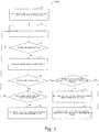
- Rectangular elements (typified by element 305 in FIG. 3 ), herein denoted “processing blocks,” represent computer software instructions or groups of instructions.
- Diamond shaped elements (typified by element 315 in FIG. 3 ), herein denoted “decision blocks,” represent computer software instructions, or groups of instructions, which affect the execution of the computer software instructions represented by the processing blocks.
- the processing and decision blocks can represent steps performed by functionally equivalent circuits such as a digital signal processor circuit or an application specific integrated circuit (ASIC).
- ASIC application specific integrated circuit
- the flow diagram does not depict the syntax of any particular programming language. Rather, the flow diagram illustrates the functional information one of ordinary skill in the art requires to fabricate circuits or to generate computer software to perform the processing required of the particular apparatus. It should be noted that many routine program elements, such as initialization of loops and variables and the use of temporary variables are not shown. It will be appreciated by those of ordinary skill in the art that unless otherwise indicated herein, the particular sequence of blocks described is illustrative only and can be varied without departing from the spirit of the invention. Thus, unless otherwise stated, the blocks described below are unordered; meaning that, when possible, the steps can be performed in any convenient or desirable order.
- a method 300 for determining an external impedance associated with an integrated circuit begins at block 305 where an external device comprising a power supply, which can be the same as or similar to device 110 of FIG. 1 , is coupled to an integrated circuit, which can be the same as or similar to integrated circuit 240 of FIG. 2 .
- a supply voltage (VCC) of the external power supply (e.g., 120, shown in FIG. 1 ) is ramped through a predetermined range of voltages.
- the supply voltage (VCC) is ramped through the predetermined range of voltages at a predetermined rate.
- the integrated circuit determines whether the comparator (e.g., comparator 252, shown in FIG. 2 ) has tripped.
- the comparator can trip, for example, when a voltage associated with the resistor divider (e.g., a voltage potential at node R) becomes greater than the threshold voltage (V TH ). If the comparator has tripped, the method proceeds to a block 320, where a current level associated with the output circuit (e.g., 260, shown in FIG. 2 ) is increased in response to a control signal.
- a transition in the control signal e.g., the logic gate output signal Cntrl in FIG.
- the method returns to a block 310, where the supply voltage (VCC) of the power supply (e.g., 120, shown in FIG. 1 ) continues to be ramped through the predetermined range of voltages.
- VCC supply voltage
- the number of times block 310 is repeated depends, at least in part, on a number of voltage levels associated with the predetermined range of voltages.
- the method proceeds to a block 320 to increase the output circuit current level, such as may occur after a predetermined delay.
- the method proceeds to a block 325, where an output signal of the integrated circuit (e.g., the current through transistor 264, shown in FIG. 2 ) is monitored for oscillation. Illustrative output signals are shown in FIG. 4 and described below. If it is determined that the output signal (e.g., 450a, shown in FIG. 4 ) is oscillating, the method proceeds to a block 340. Alternatively, if it is determined that the output signal (e.g., 405a, shown in FIG. 4 ) is not oscillating, the method proceeds to a block 330.
- an output signal of the integrated circuit e.g., the current through transistor 264, shown in FIG. 2
- Illustrative output signals are shown in FIG. 4 and described below. If it is determined that the output signal (e.g., 450a, shown in FIG. 4 ) is oscillating, the method proceeds to a block 340. Alternatively, if it is determined that the output signal (e.g., 405a, shown in
- the method proceeds to a block 335 where it is determined that the external impedance is below a first predetermined value. Alternatively, if it is determined that the supply voltage (VCC) has not been ramped through the predetermined range, the method returns to a block 310 where the supply voltage (VCC) continues to be ramped through the predetermined range of voltages. As noted above, the number of times block 310 is repeated depends, at least in part, on the number of voltages associated with the predetermined range of voltages.
- the method proceeds to a block 345 where it is determined that the external impedance is above a second predetermined value.
- the method proceeds to a block 350 where it is determined that the external impedance is between the first and second predetermined values.
- the duration of oscillation is a function of the rate of change (i.e., rate of ramping) of the VCC voltage, the comparator hysteresis, the increase/decrease in the current through transistor 264 ( FIG. 2 ), and the contact resistance.
- the IC output will oscillate for as long as it takes the VCC voltage to ramp from a first level at which VCC-IR (based on the lower output current level) shifted down by the resistor divider R1, R2 reaches the comparator threshold voltage V TH to a second level at which VCC-IR (based on the higher output current level) shifted down by the resistor divider R1, R2 reaches the comparator threshold voltage V TH minus the comparator hysteresis.
- determining the external impedance comprises determining the external impedance in response to a time of occurrence of the oscillation of the output signal, a duration of the oscillation of the output signal, or both.
- a plurality of graphs (405, 410, 415, 420, 425, 430, 435, 440, 445, 450) have a horizontal axis with a scale in time units of milliseconds (ms) and a vertical axis with a scale in current amplitude (peak-to-peak) units of milliamps (mA).
- the vertical axis is representative of output signal levels from an integrated circuit, which can be the same as or similar to integrated circuit 240 shown in FIG. 2 .
- Each of the plurality of graphs (405, 410, 415, 420, 425, 430, 435, 440, 445, 450) shows an output signal representative of an example output signal (e.g., a current signal through the output circuit 260 of FIG. 2 ) of the integrated circuit monitored at a block 325 of method 300 shown in FIG. 3 , for example, each for a different value of contact resistance 230, but over the same range of supply voltages (VCC) ramped at the same rate.
- VCC supply voltages
- the horizontal axis while labeled as time units of milliseconds, corresponds to increasing or decreasing supply voltage (VCC).
- each graph 405-450 is associated with increased contact resistance values such that graph 405 is associated with the lowest contact resistance level and graph 450 is associated with the highest contact resistance level.
- the output signals shown in graphs 405, 410, 415, 420, 425, and 430 are representative of output signals monitored by the integrated circuit and determined not to be oscillating (e.g., at a block 325 of method 300).
- an output signal substantially the same as or similar to output signal 405a shown in graph 405 for example, once the comparator trips and the output current is increased (as labeled at 405a), it is determined that the integrated circuit output is not oscillating (see, e.g., block 325 of FIG. 3 ), following which the external impedance is determined to be below a first predetermined value (e.g., block 335 of FIG. 3 ) after VCC is ramped through the full range of voltages.
- the output signals shown in graphs 435, 440, 445, and 450 are representative of output signals monitored by the integrated circuit and determined to be oscillating (e.g., at a block 325 of method 300).
- an output signal substantially the same as or similar to output signal shown in graph 450 for example, once the comparator trips (as labeled at 450a), it is determined that the integrated circuit output is oscillating (see e.g., block 325 of FIG. 3 ). Thereafter, it is determined that the oscillation has occurred for more than a predetermined time interval (e.g., block 340 of FIG. 3 ), following which it is determined that the impedance is above a second predetermined value.
- a predetermined time interval e.g., block 340 of FIG. 3
- the rate at which the supply voltage (VCC) is ramped is selected to be slow enough to enable oscillation detection, but fast enough not to require more time than necessary to perform the impedance measurement.
- embodiments of the disclosure herein may be configured as a system, method, or combination thereof. Accordingly, embodiments of the present disclosure may be comprised of various means including entirely of hardware, entirely of software, or any combination of hardware and software. Furthermore, embodiments of the present disclosure may take the form of a computer program product on a computer-readable storage medium having computer readable program instructions (e.g., computer software) embodied in the storage medium. Any suitable non-transitory computer-readable storage medium may be utilized.
Landscapes
- Engineering & Computer Science (AREA)
- Physics & Mathematics (AREA)
- General Physics & Mathematics (AREA)
- Computer Hardware Design (AREA)
- Microelectronics & Electronic Packaging (AREA)
- General Engineering & Computer Science (AREA)
- Environmental & Geological Engineering (AREA)
- Semiconductor Integrated Circuits (AREA)
Claims (16)
- Integrierte Schaltung (140; 240), umfassend:eine Ausgangsschaltung (160; 260), die einen ersten Anschluss (160a; 260a), der angepasst ist, mit einer externen Stromversorgung (120) zu koppeln, die eine Versorgungsspannung bereitstellt, welche durch einen vorbestimmten Spannungsbereich gerampt wird, einen zweiten Anschluss (160b; 260b), der angepasst ist, mit einem Bezugspotenzial zu koppeln, und einen dritten, einen Steueranschluss (160c; 260c) aufweist, wobei die ersten und zweiten Anschlüsse Ausgangsanschlüsse der integrierten Schaltung bereitstellen (140; 240); undeine Impedanzmessungsschaltung (150; 250), die auf die externe Stromversorgung anspricht und ausgeführt ist, ein Steuersignal zum Koppeln mit dem Steueranschluss (160c; 260c) der Ausgangsschaltung (160; 260) zum Steuern eines Strompegels, der mit der Ausgangsschaltung verbunden ist, zu erzeugen und um ein Ausgangssignal der integrierten Schaltung auf eine Schwingung zu überwachen,dadurch gekennzeichnet, dass die integrierte Schaltung derart ausgelegt ist, dass der gesteuerte Strompegel der Ausgangsschaltung selektiv eine Schwingung im Ausgangsstrom der integrierten Schaltung in Abhängigkeit der Spannungsänderung über einer externen Impedanz der integrierten Schaltung aufgrund der Änderung im Ausgangsstrom bewirkt, wobei die externe Impedanz für einen Widerstand bzw. Widerstände zwischen und verbunden mit der integrierten Schaltung und der externen Stromversorgung repräsentativ ist, und wobei (i) ein Zeitpunkt des Auftretens der Schwingung (ii) eine Zeitdauer der Schwingung; oder (iii) sowohl ein Zeitpunkt des Auftretens der Schwingung als auch eine Zeitdauer der Schwingung für die externe Impedanz der integrierten Schaltung indikativ ist.
- Integrierte Schaltung nach Anspruch 1, wobei die Impedanzmessungsschaltung (250) einen Widerstandsteiler umfasst, der zwischen der Stromversorgung und dem Bezugspotenzial gekoppelt ist, und einen Vergleicher (252), der auf eine mit dem Widerstandsteiler verbundene Spannung anspricht, wobei ein Ausgangssignal des Vergleichers das Steuersignal bereitstellt.
- Integrierte Schaltung nach Anspruch 1, wobei die Impedanzmessungsschaltung (250) einen Widerstandsteiler umfasst, der zwischen der Stromversorgung und dem Bezugspotenzial gekoppelt ist, wobei eine mit dem Widerstandsteiler verbundene Spannung das Steuersignal bereitstellt.
- Integrierte Schaltung nach Anspruch 2, wobei der Vergleicher (252) eine Hysterese aufweist.
- Integrierte Schaltung nach Anspruch 1, wobei das Ausgangssignal ein durch die Ausgangsschaltung (160; 260) an den Ausgangsanschlüssen der integrierten Schaltung (140; 240) bereitgestellter Strom ist.
- Integrierte Schaltung nach Anspruch 1, wobei ein Übergang im Steuersignal einen Anstieg im Strompegel der Ausgangsschaltung bewirkt.
- Integrierte Schaltung nach Anspruch 2, wobei die Impedanzmessungsschaltung (250) weiter ein Logikgatter (254) umfasst, das gekoppelt ist, um das Ausgangssignal des Vergleichers (252) als einen ersten Eingang und ein Prüfmodussignal als einen zweiten Eingang zu empfangen, wobei ein Ausgangssignal des Logikgatters das Steuersignal bereitstellt.
- Integrierte Schaltung nach Anspruch 1, wobei die Ausgangsschaltung eine Stromquelle umfasst.
- Integrierte Schaltung nach Anspruch 1, wobei die integrierte Schaltung ein Magnetfeldsensor ist.
- Integrierte Schaltung nach Anspruch 1, wobei die externe Stromversorgung eine Stromversorgung ist, die mit einer automatischen Prüfeinrichtung (ATE) verbunden ist.
- Verfahren zum Bestimmen einer externen Impedanz, die für einen Widerstand bzw. Widerstände zwischen und verbunden mit einer integrierten Schaltung (140; 240) und einer externen Stromversorgung (120) repräsentativ ist, wobei das Verfahren umfasst:Koppeln der externen Stromversorgung (120) mit der integrierten Schaltung, die eine Ausgangsschaltung (160; 260) umfasst, welche einen ersten Anschluss (160a; 260a), der angepasst ist, mit der externen Stromversorgung zu koppeln, einen zweiten Anschluss (160b; 260b), der angepasst ist, mit einem Bezugspotenzial zu koppeln, und einen dritten, einen Steueranschluss (160c; 260c) aufweist, wobei die ersten und zweiten Anschlüsse Ausgangsanschlüsse der integrierten Schaltung (140; 240) bereitstellen;Erzeugen eines Steuersignals zum Koppeln mit dem Steueranschluss (160c; 260c) der Ausgangsschaltung (160; 260) als Reaktion auf eine Versorgungsspannung von der externen Stromversorgung;Hochfahren der Versorgungsspannung der externen Stromversorgung durch einen vorbestimmten Bereich von Spannungen;Steuern eines Strompegels, der mit der Ausgangsschaltung verbunden ist, als Reaktion auf das Steuersignal; undÜberwachen eines Ausgangssignals der integrierten Schaltung auf eine Schwingung;dadurch gekennzeichnet, dass das Steuern des mit der Ausgangsschaltung verbundenen Strompegels das selektive Bewirken einer Schwingung im Ausgangsstrom der integrierten Schaltung in Abhängigkeit der Spannungsänderung über der externen Impedanz aufgrund der Änderung im Ausgangsstrom und das Bestimmen der externen Impedanz als Reaktion auf einen Zeitpunkt des Auftretens der Schwingung, eine Dauer der Schwingung oder sowohl des Zeitpunkts des Auftretens als auch der Dauer der Schwingung umfasst.
- Verfahren nach Anspruch 11, wobei das Erzeugen des Steuersignals das Vergleichen einer pegelverschobenen Version der Versorgungsspannung mit einer Schwellenspannung umfasst.
- Verfahren nach Anspruch 11, wobei das Erzeugen des Steuersignals das Pegelverschieben der Versorgungsspannung umfasst.
- Verfahren nach Anspruch 11, wobei die Ausgangsschaltung eine Stromquelle umfasst und das Überwachen des Ausgangssignals der integrierten Schaltung auf eine Schwingung das Überwachen eines Strompegels der Stromquelle umfasst.
- Verfahren nach Anspruch 11, wobei die integrierte Schaltung ein Magnetfeldsensor ist.
- Verfahren nach Anspruch 11, wobei die externe Stromversorgung eine Stromversorgung ist, die mit einer automatischen Prüfeinrichtung (ATE) verbunden ist.
Applications Claiming Priority (2)
| Application Number | Priority Date | Filing Date | Title |
|---|---|---|---|
| US14/291,597 US9575103B2 (en) | 2014-05-30 | 2014-05-30 | Integrated circuit and associated methods for measurement of an external impedance |
| PCT/US2015/031902 WO2015183680A1 (en) | 2014-05-30 | 2015-05-21 | Integrated circuit and associated method for measurement of an external impedance |
Publications (2)
| Publication Number | Publication Date |
|---|---|
| EP3134743A1 EP3134743A1 (de) | 2017-03-01 |
| EP3134743B1 true EP3134743B1 (de) | 2018-03-14 |
Family
ID=53284611
Family Applications (1)
| Application Number | Title | Priority Date | Filing Date |
|---|---|---|---|
| EP15727208.9A Active EP3134743B1 (de) | 2014-05-30 | 2015-05-21 | Integrierte schaltung und zugehöriges verfahren zur messung einer externen impedanz |
Country Status (4)
| Country | Link |
|---|---|
| US (1) | US9575103B2 (de) |
| EP (1) | EP3134743B1 (de) |
| KR (1) | KR102025590B1 (de) |
| WO (1) | WO2015183680A1 (de) |
Families Citing this family (2)
| Publication number | Priority date | Publication date | Assignee | Title |
|---|---|---|---|---|
| US10554058B2 (en) * | 2015-05-14 | 2020-02-04 | Media Tek Inc. | Systems and methods for monitoring an operating status of a connector |
| KR102816507B1 (ko) * | 2019-12-05 | 2025-06-05 | 에스케이하이닉스 주식회사 | 전원특성 측정장치, 그 전원특성 측정장치를 포함하는 이미지 시스템, 및 그 이미지 시스템의 동작 방법 |
Family Cites Families (20)
| Publication number | Priority date | Publication date | Assignee | Title |
|---|---|---|---|---|
| CH491547A (de) | 1969-09-16 | 1970-05-31 | Landis & Gyr Ag | Kippverstärkerschaltung mit mindestens einer monolithisch integrierten Kippverstärkerstufe |
| EP0352734B1 (de) | 1988-07-26 | 1993-09-29 | Siemens Aktiengesellschaft | Schaltungsanordnung zur Überwachung einer auf Null-Potential bezogenen Spannungsquelle gegenüber zwei Vergleichsspannungen |
| JP3647699B2 (ja) * | 1999-11-01 | 2005-05-18 | 株式会社東芝 | 集積回路及びロット選別システム |
| JP4002378B2 (ja) * | 1999-12-27 | 2007-10-31 | エルピーダメモリ株式会社 | 電子回路 |
| US6707312B2 (en) * | 2001-11-19 | 2004-03-16 | Micron Technology, Inc. | Pseudo variable resistor for tester platform |
| JP3574444B2 (ja) * | 2002-08-27 | 2004-10-06 | 沖電気工業株式会社 | プローブの接触抵抗測定方法及び半導体デバイスの試験方法 |
| GB2394780B (en) * | 2002-10-29 | 2006-06-14 | Ifr Ltd | A method of and apparatus for testing for integrated circuit contact defects |
| US20070080697A1 (en) * | 2005-09-27 | 2007-04-12 | Sony Corporation | Semiconductor device tester pin contact resistance measurement |
| US7411320B2 (en) | 2005-10-25 | 2008-08-12 | Bittner George E | Radially-activated engine |
| DE102006007321A1 (de) | 2006-02-16 | 2007-08-30 | Infineon Technologies Ag | Integrierte Schaltkreis-Anordnung und Verfahren zum Ermitteln des parasitären ohmschen Widerstands zumindest der Zuleitung zumindest einer Speicherzelle einer integrierten Schaltkreis-Anordnung |
| JP4798618B2 (ja) * | 2006-05-31 | 2011-10-19 | ルネサスエレクトロニクス株式会社 | 出力回路および半導体集積回路装置 |
| JP4786608B2 (ja) * | 2007-07-30 | 2011-10-05 | パナソニック株式会社 | 磁界検出装置 |
| JP5497311B2 (ja) * | 2009-03-11 | 2014-05-21 | 京セラディスプレイ株式会社 | 抵抗測定機能付ic、ic搭載パネルおよび抵抗測定方法 |
| JP2010259254A (ja) * | 2009-04-27 | 2010-11-11 | Panasonic Corp | 電流制御装置及び保護装置 |
| CN201622302U (zh) * | 2010-04-09 | 2010-11-03 | 维熹科技股份有限公司 | 过电压与过电流检测电路 |
| JP2012099199A (ja) * | 2010-11-05 | 2012-05-24 | Elpida Memory Inc | 半導体装置及びその制御方法 |
| CN102759655B (zh) | 2011-04-29 | 2016-03-16 | 飞兆半导体公司 | 多电源电压的检测电路及检测方法 |
| US9167459B2 (en) * | 2013-03-08 | 2015-10-20 | Litepoint Corporation | System and method for confirming radio frequency (RF) signal connection integrity with multiple devices under test (DUTs) to be tested concurrently |
| US20150153405A1 (en) * | 2013-12-04 | 2015-06-04 | Princeton Technology Corporation | Automatic testing system and method |
| US9568540B2 (en) * | 2014-02-28 | 2017-02-14 | International Business Machines Corporation | Method for the characterization and monitoring of integrated circuits |
-
2014
- 2014-05-30 US US14/291,597 patent/US9575103B2/en active Active
-
2015
- 2015-05-21 KR KR1020167035290A patent/KR102025590B1/ko active Active
- 2015-05-21 EP EP15727208.9A patent/EP3134743B1/de active Active
- 2015-05-21 WO PCT/US2015/031902 patent/WO2015183680A1/en not_active Ceased
Also Published As
| Publication number | Publication date |
|---|---|
| WO2015183680A1 (en) | 2015-12-03 |
| EP3134743A1 (de) | 2017-03-01 |
| KR102025590B1 (ko) | 2019-11-04 |
| US9575103B2 (en) | 2017-02-21 |
| KR20170015335A (ko) | 2017-02-08 |
| US20150346252A1 (en) | 2015-12-03 |
Similar Documents
| Publication | Publication Date | Title |
|---|---|---|
| US11313899B2 (en) | Methods and apparatus for sensor diagnostics | |
| US10527703B2 (en) | Circuits and techniques for performing self-test diagnostics in a magnetic field sensor | |
| EP2939040B1 (de) | Sensor mit fehlererkennungs- und selbsttestfunktionalität | |
| US11428731B2 (en) | Sensor integrated circuit load current monitoring circuitry and associated methods | |
| US9910087B2 (en) | Integrated circuit and method for detecting a stress condition in the integrated circuit | |
| US10156461B2 (en) | Methods and apparatus for error detection in a magnetic field sensor | |
| US10001519B2 (en) | Ground reference fault detection in circuits with multiple ground references | |
| US11555832B2 (en) | Integrated shunt and magnetic field current sensor | |
| CN102770774B (zh) | 静态电流(iddq)指示及测试装置和方法 | |
| EP3134743B1 (de) | Integrierte schaltung und zugehöriges verfahren zur messung einer externen impedanz | |
| EP3594704B1 (de) | Integrierte schaltung mit konnektivitätsfehlererkennung | |
| US11885645B2 (en) | Supply voltage configurable sensor | |
| US20250251430A1 (en) | Integrated circuit pin for reference voltage and fault communication |
Legal Events
| Date | Code | Title | Description |
|---|---|---|---|
| STAA | Information on the status of an ep patent application or granted ep patent |
Free format text: STATUS: THE INTERNATIONAL PUBLICATION HAS BEEN MADE |
|
| PUAI | Public reference made under article 153(3) epc to a published international application that has entered the european phase |
Free format text: ORIGINAL CODE: 0009012 |
|
| STAA | Information on the status of an ep patent application or granted ep patent |
Free format text: STATUS: REQUEST FOR EXAMINATION WAS MADE |
|
| 17P | Request for examination filed |
Effective date: 20161125 |
|
| AK | Designated contracting states |
Kind code of ref document: A1 Designated state(s): AL AT BE BG CH CY CZ DE DK EE ES FI FR GB GR HR HU IE IS IT LI LT LU LV MC MK MT NL NO PL PT RO RS SE SI SK SM TR |
|
| AX | Request for extension of the european patent |
Extension state: BA ME |
|
| DAV | Request for validation of the european patent (deleted) | ||
| DAX | Request for extension of the european patent (deleted) | ||
| GRAP | Despatch of communication of intention to grant a patent |
Free format text: ORIGINAL CODE: EPIDOSNIGR1 |
|
| STAA | Information on the status of an ep patent application or granted ep patent |
Free format text: STATUS: GRANT OF PATENT IS INTENDED |
|
| INTG | Intention to grant announced |
Effective date: 20171113 |
|
| GRAS | Grant fee paid |
Free format text: ORIGINAL CODE: EPIDOSNIGR3 |
|
| GRAA | (expected) grant |
Free format text: ORIGINAL CODE: 0009210 |
|
| STAA | Information on the status of an ep patent application or granted ep patent |
Free format text: STATUS: THE PATENT HAS BEEN GRANTED |
|
| AK | Designated contracting states |
Kind code of ref document: B1 Designated state(s): AL AT BE BG CH CY CZ DE DK EE ES FI FR GB GR HR HU IE IS IT LI LT LU LV MC MK MT NL NO PL PT RO RS SE SI SK SM TR |
|
| REG | Reference to a national code |
Ref country code: GB Ref legal event code: FG4D |
|
| REG | Reference to a national code |
Ref country code: CH Ref legal event code: EP Ref country code: AT Ref legal event code: REF Ref document number: 979413 Country of ref document: AT Kind code of ref document: T Effective date: 20180315 |
|
| REG | Reference to a national code |
Ref country code: IE Ref legal event code: FG4D |
|
| REG | Reference to a national code |
Ref country code: DE Ref legal event code: R096 Ref document number: 602015008877 Country of ref document: DE |
|
| REG | Reference to a national code |
Ref country code: NL Ref legal event code: MP Effective date: 20180314 |
|
| REG | Reference to a national code |
Ref country code: LT Ref legal event code: MG4D |
|
| PG25 | Lapsed in a contracting state [announced via postgrant information from national office to epo] |
Ref country code: HR Free format text: LAPSE BECAUSE OF FAILURE TO SUBMIT A TRANSLATION OF THE DESCRIPTION OR TO PAY THE FEE WITHIN THE PRESCRIBED TIME-LIMIT Effective date: 20180314 Ref country code: CY Free format text: LAPSE BECAUSE OF FAILURE TO SUBMIT A TRANSLATION OF THE DESCRIPTION OR TO PAY THE FEE WITHIN THE PRESCRIBED TIME-LIMIT Effective date: 20180314 Ref country code: LT Free format text: LAPSE BECAUSE OF FAILURE TO SUBMIT A TRANSLATION OF THE DESCRIPTION OR TO PAY THE FEE WITHIN THE PRESCRIBED TIME-LIMIT Effective date: 20180314 Ref country code: FI Free format text: LAPSE BECAUSE OF FAILURE TO SUBMIT A TRANSLATION OF THE DESCRIPTION OR TO PAY THE FEE WITHIN THE PRESCRIBED TIME-LIMIT Effective date: 20180314 Ref country code: NO Free format text: LAPSE BECAUSE OF FAILURE TO SUBMIT A TRANSLATION OF THE DESCRIPTION OR TO PAY THE FEE WITHIN THE PRESCRIBED TIME-LIMIT Effective date: 20180614 |
|
| RAP2 | Party data changed (patent owner data changed or rights of a patent transferred) |
Owner name: ALLEGRO MICROSYSTEMS, LLC |
|
| REG | Reference to a national code |
Ref country code: AT Ref legal event code: MK05 Ref document number: 979413 Country of ref document: AT Kind code of ref document: T Effective date: 20180314 |
|
| PG25 | Lapsed in a contracting state [announced via postgrant information from national office to epo] |
Ref country code: RS Free format text: LAPSE BECAUSE OF FAILURE TO SUBMIT A TRANSLATION OF THE DESCRIPTION OR TO PAY THE FEE WITHIN THE PRESCRIBED TIME-LIMIT Effective date: 20180314 Ref country code: GR Free format text: LAPSE BECAUSE OF FAILURE TO SUBMIT A TRANSLATION OF THE DESCRIPTION OR TO PAY THE FEE WITHIN THE PRESCRIBED TIME-LIMIT Effective date: 20180615 Ref country code: LV Free format text: LAPSE BECAUSE OF FAILURE TO SUBMIT A TRANSLATION OF THE DESCRIPTION OR TO PAY THE FEE WITHIN THE PRESCRIBED TIME-LIMIT Effective date: 20180314 Ref country code: SE Free format text: LAPSE BECAUSE OF FAILURE TO SUBMIT A TRANSLATION OF THE DESCRIPTION OR TO PAY THE FEE WITHIN THE PRESCRIBED TIME-LIMIT Effective date: 20180314 Ref country code: BG Free format text: LAPSE BECAUSE OF FAILURE TO SUBMIT A TRANSLATION OF THE DESCRIPTION OR TO PAY THE FEE WITHIN THE PRESCRIBED TIME-LIMIT Effective date: 20180614 |
|
| PG25 | Lapsed in a contracting state [announced via postgrant information from national office to epo] |
Ref country code: ES Free format text: LAPSE BECAUSE OF FAILURE TO SUBMIT A TRANSLATION OF THE DESCRIPTION OR TO PAY THE FEE WITHIN THE PRESCRIBED TIME-LIMIT Effective date: 20180314 Ref country code: NL Free format text: LAPSE BECAUSE OF FAILURE TO SUBMIT A TRANSLATION OF THE DESCRIPTION OR TO PAY THE FEE WITHIN THE PRESCRIBED TIME-LIMIT Effective date: 20180314 Ref country code: AL Free format text: LAPSE BECAUSE OF FAILURE TO SUBMIT A TRANSLATION OF THE DESCRIPTION OR TO PAY THE FEE WITHIN THE PRESCRIBED TIME-LIMIT Effective date: 20180314 Ref country code: EE Free format text: LAPSE BECAUSE OF FAILURE TO SUBMIT A TRANSLATION OF THE DESCRIPTION OR TO PAY THE FEE WITHIN THE PRESCRIBED TIME-LIMIT Effective date: 20180314 Ref country code: IT Free format text: LAPSE BECAUSE OF FAILURE TO SUBMIT A TRANSLATION OF THE DESCRIPTION OR TO PAY THE FEE WITHIN THE PRESCRIBED TIME-LIMIT Effective date: 20180314 Ref country code: RO Free format text: LAPSE BECAUSE OF FAILURE TO SUBMIT A TRANSLATION OF THE DESCRIPTION OR TO PAY THE FEE WITHIN THE PRESCRIBED TIME-LIMIT Effective date: 20180314 Ref country code: PL Free format text: LAPSE BECAUSE OF FAILURE TO SUBMIT A TRANSLATION OF THE DESCRIPTION OR TO PAY THE FEE WITHIN THE PRESCRIBED TIME-LIMIT Effective date: 20180314 |
|
| PG25 | Lapsed in a contracting state [announced via postgrant information from national office to epo] |
Ref country code: SK Free format text: LAPSE BECAUSE OF FAILURE TO SUBMIT A TRANSLATION OF THE DESCRIPTION OR TO PAY THE FEE WITHIN THE PRESCRIBED TIME-LIMIT Effective date: 20180314 Ref country code: CZ Free format text: LAPSE BECAUSE OF FAILURE TO SUBMIT A TRANSLATION OF THE DESCRIPTION OR TO PAY THE FEE WITHIN THE PRESCRIBED TIME-LIMIT Effective date: 20180314 Ref country code: AT Free format text: LAPSE BECAUSE OF FAILURE TO SUBMIT A TRANSLATION OF THE DESCRIPTION OR TO PAY THE FEE WITHIN THE PRESCRIBED TIME-LIMIT Effective date: 20180314 Ref country code: SM Free format text: LAPSE BECAUSE OF FAILURE TO SUBMIT A TRANSLATION OF THE DESCRIPTION OR TO PAY THE FEE WITHIN THE PRESCRIBED TIME-LIMIT Effective date: 20180314 |
|
| REG | Reference to a national code |
Ref country code: CH Ref legal event code: PL |
|
| REG | Reference to a national code |
Ref country code: DE Ref legal event code: R097 Ref document number: 602015008877 Country of ref document: DE |
|
| PG25 | Lapsed in a contracting state [announced via postgrant information from national office to epo] |
Ref country code: PT Free format text: LAPSE BECAUSE OF FAILURE TO SUBMIT A TRANSLATION OF THE DESCRIPTION OR TO PAY THE FEE WITHIN THE PRESCRIBED TIME-LIMIT Effective date: 20180716 |
|
| PLBE | No opposition filed within time limit |
Free format text: ORIGINAL CODE: 0009261 |
|
| STAA | Information on the status of an ep patent application or granted ep patent |
Free format text: STATUS: NO OPPOSITION FILED WITHIN TIME LIMIT |
|
| REG | Reference to a national code |
Ref country code: BE Ref legal event code: MM Effective date: 20180531 |
|
| PG25 | Lapsed in a contracting state [announced via postgrant information from national office to epo] |
Ref country code: DK Free format text: LAPSE BECAUSE OF FAILURE TO SUBMIT A TRANSLATION OF THE DESCRIPTION OR TO PAY THE FEE WITHIN THE PRESCRIBED TIME-LIMIT Effective date: 20180314 Ref country code: MC Free format text: LAPSE BECAUSE OF FAILURE TO SUBMIT A TRANSLATION OF THE DESCRIPTION OR TO PAY THE FEE WITHIN THE PRESCRIBED TIME-LIMIT Effective date: 20180314 |
|
| 26N | No opposition filed |
Effective date: 20181217 |
|
| REG | Reference to a national code |
Ref country code: IE Ref legal event code: MM4A |
|
| PG25 | Lapsed in a contracting state [announced via postgrant information from national office to epo] |
Ref country code: LI Free format text: LAPSE BECAUSE OF NON-PAYMENT OF DUE FEES Effective date: 20180531 Ref country code: SI Free format text: LAPSE BECAUSE OF FAILURE TO SUBMIT A TRANSLATION OF THE DESCRIPTION OR TO PAY THE FEE WITHIN THE PRESCRIBED TIME-LIMIT Effective date: 20180314 Ref country code: CH Free format text: LAPSE BECAUSE OF NON-PAYMENT OF DUE FEES Effective date: 20180531 |
|
| PG25 | Lapsed in a contracting state [announced via postgrant information from national office to epo] |
Ref country code: LU Free format text: LAPSE BECAUSE OF NON-PAYMENT OF DUE FEES Effective date: 20180521 |
|
| PG25 | Lapsed in a contracting state [announced via postgrant information from national office to epo] |
Ref country code: IE Free format text: LAPSE BECAUSE OF NON-PAYMENT OF DUE FEES Effective date: 20180521 Ref country code: FR Free format text: LAPSE BECAUSE OF NON-PAYMENT OF DUE FEES Effective date: 20180531 |
|
| PG25 | Lapsed in a contracting state [announced via postgrant information from national office to epo] |
Ref country code: BE Free format text: LAPSE BECAUSE OF NON-PAYMENT OF DUE FEES Effective date: 20180531 |
|
| GBPC | Gb: european patent ceased through non-payment of renewal fee |
Effective date: 20190521 |
|
| PG25 | Lapsed in a contracting state [announced via postgrant information from national office to epo] |
Ref country code: MT Free format text: LAPSE BECAUSE OF NON-PAYMENT OF DUE FEES Effective date: 20180521 |
|
| PG25 | Lapsed in a contracting state [announced via postgrant information from national office to epo] |
Ref country code: TR Free format text: LAPSE BECAUSE OF FAILURE TO SUBMIT A TRANSLATION OF THE DESCRIPTION OR TO PAY THE FEE WITHIN THE PRESCRIBED TIME-LIMIT Effective date: 20180314 |
|
| PG25 | Lapsed in a contracting state [announced via postgrant information from national office to epo] |
Ref country code: GB Free format text: LAPSE BECAUSE OF NON-PAYMENT OF DUE FEES Effective date: 20190521 |
|
| PG25 | Lapsed in a contracting state [announced via postgrant information from national office to epo] |
Ref country code: MK Free format text: LAPSE BECAUSE OF NON-PAYMENT OF DUE FEES Effective date: 20180314 Ref country code: HU Free format text: LAPSE BECAUSE OF FAILURE TO SUBMIT A TRANSLATION OF THE DESCRIPTION OR TO PAY THE FEE WITHIN THE PRESCRIBED TIME-LIMIT; INVALID AB INITIO Effective date: 20150521 |
|
| PG25 | Lapsed in a contracting state [announced via postgrant information from national office to epo] |
Ref country code: IS Free format text: LAPSE BECAUSE OF FAILURE TO SUBMIT A TRANSLATION OF THE DESCRIPTION OR TO PAY THE FEE WITHIN THE PRESCRIBED TIME-LIMIT Effective date: 20180714 |
|
| PGFP | Annual fee paid to national office [announced via postgrant information from national office to epo] |
Ref country code: DE Payment date: 20250325 Year of fee payment: 11 |