EP3093885A1 - Semiconductor device and semiconductor device manufacturing method - Google Patents
Semiconductor device and semiconductor device manufacturing method Download PDFInfo
- Publication number
- EP3093885A1 EP3093885A1 EP15862153.2A EP15862153A EP3093885A1 EP 3093885 A1 EP3093885 A1 EP 3093885A1 EP 15862153 A EP15862153 A EP 15862153A EP 3093885 A1 EP3093885 A1 EP 3093885A1
- Authority
- EP
- European Patent Office
- Prior art keywords
- spacer
- heat dissipation
- heatsink
- semiconductor device
- wiring
- Prior art date
- Legal status (The legal status is an assumption and is not a legal conclusion. Google has not performed a legal analysis and makes no representation as to the accuracy of the status listed.)
- Granted
Links
Images


Classifications
-
- H—ELECTRICITY
- H10—SEMICONDUCTOR DEVICES; ELECTRIC SOLID-STATE DEVICES NOT OTHERWISE PROVIDED FOR
- H10W—GENERIC PACKAGES, INTERCONNECTIONS, CONNECTORS OR OTHER CONSTRUCTIONAL DETAILS OF DEVICES COVERED BY CLASS H10
- H10W40/00—Arrangements for thermal protection or thermal control
- H10W40/20—Arrangements for cooling
- H10W40/22—Arrangements for cooling characterised by their shape, e.g. having conical or cylindrical projections
- H10W40/226—Arrangements for cooling characterised by their shape, e.g. having conical or cylindrical projections characterised by projecting parts, e.g. fins to increase surface area
- H10W40/228—Arrangements for cooling characterised by their shape, e.g. having conical or cylindrical projections characterised by projecting parts, e.g. fins to increase surface area the projecting parts being wire-shaped or pin-shaped
-
- H—ELECTRICITY
- H10—SEMICONDUCTOR DEVICES; ELECTRIC SOLID-STATE DEVICES NOT OTHERWISE PROVIDED FOR
- H10W—GENERIC PACKAGES, INTERCONNECTIONS, CONNECTORS OR OTHER CONSTRUCTIONAL DETAILS OF DEVICES COVERED BY CLASS H10
- H10W40/00—Arrangements for thermal protection or thermal control
- H10W40/60—Securing means for detachable heating or cooling arrangements, e.g. clamps
- H10W40/611—Bolts or screws
-
- H—ELECTRICITY
- H10—SEMICONDUCTOR DEVICES; ELECTRIC SOLID-STATE DEVICES NOT OTHERWISE PROVIDED FOR
- H10W—GENERIC PACKAGES, INTERCONNECTIONS, CONNECTORS OR OTHER CONSTRUCTIONAL DETAILS OF DEVICES COVERED BY CLASS H10
- H10W40/00—Arrangements for thermal protection or thermal control
- H10W40/01—Manufacture or treatment
- H10W40/03—Manufacture or treatment of arrangements for cooling
- H10W40/037—Assembling together parts thereof
-
- H—ELECTRICITY
- H10—SEMICONDUCTOR DEVICES; ELECTRIC SOLID-STATE DEVICES NOT OTHERWISE PROVIDED FOR
- H10W—GENERIC PACKAGES, INTERCONNECTIONS, CONNECTORS OR OTHER CONSTRUCTIONAL DETAILS OF DEVICES COVERED BY CLASS H10
- H10W40/00—Arrangements for thermal protection or thermal control
- H10W40/20—Arrangements for cooling
- H10W40/22—Arrangements for cooling characterised by their shape, e.g. having conical or cylindrical projections
-
- H—ELECTRICITY
- H10—SEMICONDUCTOR DEVICES; ELECTRIC SOLID-STATE DEVICES NOT OTHERWISE PROVIDED FOR
- H10W—GENERIC PACKAGES, INTERCONNECTIONS, CONNECTORS OR OTHER CONSTRUCTIONAL DETAILS OF DEVICES COVERED BY CLASS H10
- H10W70/00—Package substrates; Interposers; Redistribution layers [RDL]
- H10W70/60—Insulating or insulated package substrates; Interposers; Redistribution layers
-
- H—ELECTRICITY
- H10—SEMICONDUCTOR DEVICES; ELECTRIC SOLID-STATE DEVICES NOT OTHERWISE PROVIDED FOR
- H10W—GENERIC PACKAGES, INTERCONNECTIONS, CONNECTORS OR OTHER CONSTRUCTIONAL DETAILS OF DEVICES COVERED BY CLASS H10
- H10W95/00—Packaging processes not covered by the other groups of this subclass
-
- H—ELECTRICITY
- H10—SEMICONDUCTOR DEVICES; ELECTRIC SOLID-STATE DEVICES NOT OTHERWISE PROVIDED FOR
- H10W—GENERIC PACKAGES, INTERCONNECTIONS, CONNECTORS OR OTHER CONSTRUCTIONAL DETAILS OF DEVICES COVERED BY CLASS H10
- H10W40/00—Arrangements for thermal protection or thermal control
- H10W40/20—Arrangements for cooling
- H10W40/231—Arrangements for cooling characterised by their places of attachment or cooling paths
- H10W40/237—Arrangements for cooling characterised by their places of attachment or cooling paths attached to additional arrangements for cooling
-
- H—ELECTRICITY
- H10—SEMICONDUCTOR DEVICES; ELECTRIC SOLID-STATE DEVICES NOT OTHERWISE PROVIDED FOR
- H10W—GENERIC PACKAGES, INTERCONNECTIONS, CONNECTORS OR OTHER CONSTRUCTIONAL DETAILS OF DEVICES COVERED BY CLASS H10
- H10W40/00—Arrangements for thermal protection or thermal control
- H10W40/60—Securing means for detachable heating or cooling arrangements, e.g. clamps
Definitions
- the present invention relates to a semiconductor device and a manufacturing method of a semiconductor device, and particularly relates to a heat dissipation structure for a power element.
- Patent Literature 1 discloses a configuration in which spacers are disposed under elements to which a heatsink is attached.
- the configuration is such that the spacers are used in order to align the height of the heat dissipation surfaces of the elements and heat is dissipated only from the heatsink disposed on the top surface side of the elements.
- Patent Literature 2 discloses a device in which heat generation elements are secured to the printed board such that they are sandwiched between a base unit for cooling the heat generation elements and a holder from which the heatsink is configured.
- Patent Literature 1 heat is dissipated only from the heatsink secured to the top surface side of the elements.
- Patent Literature 2 heat is dissipated from the heatsink and the base unit, between which the power elements are sandwiched from above and below to secure the power elements.
- heat is mainly dissipated from the heatsink secured to the top surface side of the power elements, and heat is not expected to be dissipated from the spacers or the base unit mounted on the board side, which is the bottom surface side of the power elements, or the base unit does not have a structure that can dissipate heat efficiently.
- the present invention has been achieved in view of the above and an object of the present invention is to provide a semiconductor device that can improve the efficiency of dissipating heat from the bottom surface side of a semiconductor element and that can provide excellent heat dissipation characteristics without increasing the size of the heatsink on the top surface side.
- a semiconductor device includes a wiring board that includes a wiring layer including a wiring portion and a back-surface-side heat dissipation portion; a semiconductor element that is mounted on a first main surface of the wiring board and is connected to the wiring portion; a spacer that is interposed between the semiconductor element and the first main surface of the wiring board and is connected to the back-surface-side heat dissipation portion; and a heatsink that sandwiches, together with the spacer, the semiconductor element and is secured to the spacer.
- the wiring board includes an insulating board having the first main surface and a second main surface, which is on the opposite side of the first main surface, and the wiring layer including the wiring portion and the back-surface-side heat dissipation portion formed on the second main surface.
- an effect is obtained where it is possible to improve the efficiency of dissipating heat from the bottom surface side of a semiconductor element and provide excellent heat dissipation characteristics without increasing the size of the heatsink on the top surface side.
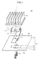
- FIG. 1 is an exploded perspective view illustrating a control device, which is a semiconductor device according to a first embodiment
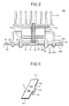
- FIG. 2 is an explanatory cross-sectional view of the semiconductor device
- FIG. 3 is a perspective view illustrating a spacer of the semiconductor device according to the first embodiment
- FIG. 4 is a perspective view illustrating a power module, the heat of which is dissipated from the semiconductor device according to the first embodiment
- FIG. 5 is a perspective view illustrating a heatsink of the semiconductor device according to the first embodiment
- FIG. 6 is an explanatory cross-sectional view of a wiring board of the semiconductor device according to the first embodiment.
- a control device 100 in the first embodiment is configured such that heat is dissipated from a spacer 40 provided under a power element 10 and heat is conducted from the spacer 40 to a heat dissipation portion 35H made of a wiring layer 35 provided on a back surface 30B side of a wiring board 30, which is a solder formed surface side, so as to enable the heat to be dissipated also from the pattern on the solder formed surface side of the wiring board 30.
- the back surface 30B of the wiring board 30 is the surface on the opposite side of an element mounting surface 30A on which the power element 10 is mounted.
- the power element 10 that generates heat is sandwiched between a heatsink 20 and the spacer 40 and is fastened with heatsink securing screws 50 so as to be secured under compression.
- the power element 10 releases heat from the top surface side.
- the spacer 40 keeps the height from the bottom surface side of the power element 10 to the surface of the wiring board 30 constant.
- the power element 10 to which the heatsink 20 and the spacer 40 are secured is mounted on the wiring board 30 and is secured with a solder layer 60.
- the wiring board 30 has power-element mounting holes 32 and spacer mounting holes 33 formed therein.
- the heat dissipation device includes the heatsink 20, which dissipates the heat of the power element 10 to the top surface, and the spacer 40, which conducts the heat to the bottom surface.
- the control device 100 in particular, establishes a path for dissipating heat from the spacer 40.
- the spacer 40 is formed from a metal plate on which the solder layer 60 can be formed.
- a copper plate plated with a nickel layer or gold can be used.
- the spacer 40 includes a spacer body 41 and vertical pieces 42, which are bent and stand vertical on both sides of the central portion of the spacer body 41. The height of the vertical pieces 42 is adjustable. Projections 43 are formed at the tips of the vertical pieces 42. The projections 43 are guided through the spacer mounting holes 33 in the wiring board 30 to the back surface 30B side and are secured, with the solder layer 60, to the heat dissipation portion 35H of the wiring layer 35 formed on the back surface 30B side.
- the spacer 40 With the projections 43, the spacer 40 is positioned and secured on the wiring board 30 and releases the heat received from the power element 10 mounted on the element mounting surface 30A, which is the first main surface, to the heat dissipation portion 35H made of the copper-foil wiring pattern 35 formed on the back surface 30B side of the wiring board 30, which is the second main surface side.
- Free ends 41T of the spacer body 41 may project to the lateral sides of the power element 10 so as to have a function of dissipating heat to the lateral sides.
- Mounting holes 44 are provided in the spacer body 41.
- the power element 10 includes an element body 11 made of a resin package in which a power semiconductor chip (not illustrated) is sealed and a plurality of lead terminals 12 led out from the element body 11. Notches 13 for positioning are formed on the surfaces orthogonal to the lead terminal lead-out surfaces.
- the heatsink securing screws 50 that pass through the heatsink 20 and the spacer 40 are brought into contact with the notches 13 from both sides; therefore, the power element 10 is sandwiched between the heatsink securing screws 50 so as to be secured.
- the heatsink 20 includes a heatsink body 21, which is brought into contact with the power element 10, and a plurality of fins 22, which extend from the heatsink body 21.
- the heatsink 20 has mounting holes 23 provided in the heatsink body 21. The heatsink securing screws 50 are screwed into the mounting holes 23.
- the power-element mounting holes 32 and the spacer mounting holes 33 are formed in the element mounting region of an insulating board 31, such as an epoxy board.
- the pattern of the wiring layer 35 is formed on the back surface 30B side of the insulating board 31.
- the wiring layer 35 is formed by patterning a copper foil and the heat dissipation portion 35H made of a solid pattern is formed immediately below the power element 10.
- the heat dissipation performance is further improved. Provision of the screw holes 34 for allowing the heatsink securing screws 50 to pass therethrough enables the heatsink 20 to be secured with the heatsink securing screws 50 after the power element 10 and the spacer 40 are secured with the solder layer 60.
- the wiring board 30 illustrated in FIG. 6 is first prepared and the spacer 40, the power element 10, which is a semiconductor element, and the heatsink 20 are stacked on the first main surface, which is the element mounting surface 30A of the wiring board 30, in the order they appear in this sentence.
- the projections 43 of the spacer 40 are first inserted into the spacer mounting holes 33 in the wiring board 30.
- the tips of the projections 43 are bent inwardly if necessary onto the back surface 30B of the wiring board 30 so as to bring the projections 43 into contact with the heat dissipation portion 35H, and then the projections 43 are connected to the heat dissipation portion 35H with the solder layer 60.
- the lead terminals 12 of the power element 10 are inserted into the power-element-mounting holes 32 and are connected to the wiring layer 35, of which the wiring portion 35C formed on the back surface 30B is made, with the solder layer 60.
- the heat dissipation portion 35H and the region to which the lead terminals 12 are connected are electrically separated from each other, it is also possible to connect one of the lead terminals 12 to the heat dissipation portion 35H and use the heat dissipation portion 35H as part of the ground plate.
- the process of connecting the lead terminals 12 of the power element 10 to the wiring portion 35C with the solder layer 60 and the process of connecting the projections 43 of the spacer 40 to the heat dissipation portion 35H can be performed during the same thermal process by collectively heating solder after the solder is supplied.
- solder connection can be performed by performing the thermal process without supplying solder.
- the heatsink 20 is mounted on a first main surface 10A side of the power element 10 and the spacer body 41 of the spacer 40 is thermally connected to the heat dissipation portion on the back surface side of the power element 10.
- the heatsink securing screws 50 pass through the mounting holes 44 provided in the spacer body 41 of the spacer 40 from the screw holes 34 for allowing the heatsink securing screws 50 to pass therethrough, come into contact with the notches 13 of the power element 10, pass up to the mounting holes 23 provided in the heatsink body 21 of the heatsink 20, and are then screwed into the screw grooves formed on the mounting holes 23 in the heatsink 20 so as to be secured.
- the power element 10 is sandwiched between the heatsink 20 and the spacer 40 and is secured with the heatsink securing screws 50.
- Thermally conductive sheets 70 are interposed between the respective contact surfaces so that the efficiency of conducting heat from the power element 10 to the heatsink 20 and the spacer 40 increases.
- Thermally conductive grease may be injected instead of providing the thermally conductive sheets 70.
- the heatsink securing screws 50 may be secured with nuts (not illustrated).
- the spacer 40 is formed such that the free ends 41T of the spacer body 41 project to the lateral sides of the power element 10 so as to have a function of dissipating heat to the lateral sides. With this configuration, the area of contact with the air increases, thereby enabling the heat dissipation effect to be improved.
- the heat conducted to the spacer 40 from the power element 10 is then conducted to the wiring layer 35 formed on the back surface 30B of the wiring board 30 via the solder layer 60, the heat dissipation effect can be improved by increasing the area of the heat dissipation portion 35H to which the heat is conducted and which is made of the wiring layer 35 of the wiring board 30.
- heat can be efficiently conducted and dissipated from the spacer 40 to the heat dissipation portion 35H made of the wiring layer 35 formed on the back surface 30B of the wiring board 30; therefore, the heatsink 20 can be prevented from being increased in size. Therefore, it is possible to prevent an increase in the cost of the heatsink and addition of a structure for holding the enlarged heatsink.
- the heat dissipation portion 35H is provided on the wiring layer side, i.e., on the back surface 30B side of the wiring board 30, and heat can be dissipated also from the heat dissipation portion 35H; therefore, addition of a dedicated part for heat dissipation is not necessary and thus heat can be easily and efficiently dissipated.
- a heat dissipation path is provided, which is for conducting heat of the power element 10 to the back surface 30B, which is on the opposite side of the element mounting surface 30A of the wiring board 30, and for dissipating the heat from the heat dissipation portion 35H. Therefore, heat can be efficiently dissipated from both sides of the power element 10. Furthermore, an effect is obtained where the heat dissipation efficiency of the control device can be improved without increasing the cost and thus the heatsink can be prevented from being increased in size.
- a wiring layer is provided only on the back surface side of the wiring board, i.e., a single-sided pattern is applied; however, a wiring layer does not necessarily need to be provided only on one side and a double-sided pattern may be applied.
- a multilayer wiring board may be used. With the use of a multilayer wiring board, it is possible to, for example, form a heat dissipation path for conducting heat to the peripheral portion of the board by using an intermediate conductor.
- the lead terminals of the power element can be connected to the wiring layer on the element mounting surface side in accordance with where the wiring layer is provided. In other words, connection of the lead terminals to the wiring layer can be appropriately modified.
- FIG. 7 is an exploded perspective view illustrating the control device 100, which is a semiconductor device according to a second embodiment;
- FIG. 8 is an explanatory cross-sectional view of the semiconductor device;
- FIG. 9 is an explanatory cross-sectional view of a wiring board of the semiconductor device according to the second embodiment.
- the pattern of a wiring layer 35A which comes into contact with the spacer 40, is provided on the element mounting surface 30A of the wiring board 30, on which the power substrate 10 is mounted.
- the wiring layer 35A is provided with a plurality of through holes 36, through which the wiring layer 35A on the element mounting surface 30A of the wiring board 30, on which the power element 10 is mounted, and a wiring layer 35B on the back surface 30B side communicate with each other, thereby enabling heat to be conducted.
- the spacer 40 is similar to that in the first embodiment; however, the spacer 40 includes the projections 43 for positioning and securing it on the wiring board 30.
- the wiring board 30 is provided with the screw holes 34 for allowing the heatsink securing screws 50 to pass therethrough.
- the spacer 40 is secured to the wiring board 30 without using the solder layer 60; therefore, it can be made of metal, such as aluminum, to which solder is not easily adhered.
- the top surface of the spacer 40 is in contact with the power element 10 and the bottom surface of the spacer 40 is in contact with the wiring layer 35A of the wiring board 30.
- the assembling method is similar to the assembling method of the control device 100 according to the first embodiment; however, in the control device 100 according to the second embodiment, the spacer 40 is brought into contact with the front-surface-side heat dissipation portion made of the wiring layer 35A on the element mounting surface 30A side of the wiring board 30. In order to efficiently conduct heat between the spacer 40 and the wiring board 30, the power element 10 and the spacer 40 are sandwiched between the heatsink 20 and the wiring board 30 and are secured with the heatsink securing screws 50. In the control device 100 according to the second embodiment also, the thermally conductive sheets 70 are interposed between the respective contact surfaces so that the efficiency of conducting heat from the power element 10 to the heatsink 20 and the spacer 40 increases.
- the heat dissipation path increases, which is for receiving heat from the spacer 40 by the front-surface-side heat dissipation portion made of the wiring layer 35A on the element mounting surface 30A side of the wiring board 30 and for conducting the heat to the heat dissipation portion 35H on the back surface 30B side via the through holes 36. Therefore, an effect is obtained where the heat dissipation performance is further improved compared with the control device 100 in the first embodiment.
- Thermally conductive grease may be injected instead of providing the thermally conductive sheets 70.
- the heatsink securing screws 50 may be secured with nuts (not illustrated).
- the spacer 40 may pass through the wiring board 30 or may be secured on the element mounting surface 30A side.
- the spacer 40 can be secured by using an adhesive having excellent thermal conductivity, by crimping, or by using other methods. However, when the spacer 40 is secured on the element mounting surface 30A side, it is desirable to secure the spacer 40 with an adhesive.
- the wiring layer 35 of the wiring board 30 is formed with a double-sided pattern provided on both sides, i.e., the element mounting surface 30A side and the back surface 30B side.
- a wiring layer does not necessarily need to be provided on both sides and a single-sided pattern may be applied. It is satisfactory if the spacer 40 is thermally in contact with at least any of the front-surface-side heat dissipation portion made of the wiring layer 35A and the back-surface-side heat dissipation portion made of the wiring layer 35B.
- thermal connection between the heat dissipation portions on both sides is realized via the through holes 36 for forming the heat dissipation path and the heat from the spacer 40 is conducted to the back surface 30B side of the wiring board 30.
- a multilayer wiring board may be used.
- the lead terminals 12 of the power element 10 can be connected to the wiring layer 35 on the element mounting surface 30A side.
- two heatsink securing screws 50 are provided and they are caused to match the notches 13 provided on both sides of the element body 11 of the power element 10 so as to secure it while being positioned.
- the structure is not limited thereto.
- one through hole may be formed in the center of the element body 11 and the heatsink securing screw 50 may be inserted through this through hole so as to be secured. With this structure, assembling is facilitated.
Landscapes
- Cooling Or The Like Of Semiconductors Or Solid State Devices (AREA)
- Cooling Or The Like Of Electrical Apparatus (AREA)
Abstract
Description
- The present invention relates to a semiconductor device and a manufacturing method of a semiconductor device, and particularly relates to a heat dissipation structure for a power element.
- Conventional control devices use heatsinks or spacers to dissipate heat of a high-heat-generation element, such as a power element. Patent Literature 1, for example, discloses a configuration in which spacers are disposed under elements to which a heatsink is attached. In Patent Literature 1, the configuration is such that the spacers are used in order to align the height of the heat dissipation surfaces of the elements and heat is dissipated only from the heatsink disposed on the top surface side of the elements.
- Moreover, Patent Literature 2 discloses a device in which heat generation elements are secured to the printed board such that they are sandwiched between a base unit for cooling the heat generation elements and a holder from which the heatsink is configured.
-
- Patent Literature 1:
Japanese Patent Application Laid-open No. 2004-95697 - Patent Literature 2:
Japanese Patent Application Laid-open No. 2011-199044 - In Patent Literature 1 described above, however, heat is dissipated only from the heatsink secured to the top surface side of the elements. Moreover, in Patent Literature 2, heat is dissipated from the heatsink and the base unit, between which the power elements are sandwiched from above and below to secure the power elements. In the technologies disclosed in Patent Literature 1 and Patent Literature 2, heat is mainly dissipated from the heatsink secured to the top surface side of the power elements, and heat is not expected to be dissipated from the spacers or the base unit mounted on the board side, which is the bottom surface side of the power elements, or the base unit does not have a structure that can dissipate heat efficiently. Thus, in order to dissipate heat more efficiently, it has been necessary to increase the size of the fins of the heatsink on the top surface side. Moreover, a structure for supporting the enlarged heatsink is necessary. Furthermore, the heatsink vibrates because of the vibrations of the unit and thus a force is applied to the power elements, which may result in breaking the leads of the power elements or damaging the soldered portions.
- The present invention has been achieved in view of the above and an object of the present invention is to provide a semiconductor device that can improve the efficiency of dissipating heat from the bottom surface side of a semiconductor element and that can provide excellent heat dissipation characteristics without increasing the size of the heatsink on the top surface side.
- In order to solve the above problems and achieve the object, a semiconductor device according to an aspect of the present invention includes a wiring board that includes a wiring layer including a wiring portion and a back-surface-side heat dissipation portion; a semiconductor element that is mounted on a first main surface of the wiring board and is connected to the wiring portion; a spacer that is interposed between the semiconductor element and the first main surface of the wiring board and is connected to the back-surface-side heat dissipation portion; and a heatsink that sandwiches, together with the spacer, the semiconductor element and is secured to the spacer. The wiring board includes an insulating board having the first main surface and a second main surface, which is on the opposite side of the first main surface, and the wiring layer including the wiring portion and the back-surface-side heat dissipation portion formed on the second main surface.
- According to the present invention, an effect is obtained where it is possible to improve the efficiency of dissipating heat from the bottom surface side of a semiconductor element and provide excellent heat dissipation characteristics without increasing the size of the heatsink on the top surface side.
-
-
FIG. 1 is an exploded perspective view illustrating a semiconductor device according to a first embodiment. -
FIG. 2 is an explanatory cross-sectional view of the semiconductor device according to the first embodiment. -
FIG. 3 is a perspective view illustrating a spacer of the semiconductor device according to the first embodiment. -
FIG. 4 is a perspective view illustrating a power module, the heat of which is dissipated from the semiconductor device according to the first embodiment. -
FIG. 5 is a perspective view illustrating a heatsink of the semiconductor device according to the first embodiment. -
FIG. 6 is an explanatory cross-sectional view of a wiring board of the semiconductor device according to the first embodiment. -
FIG. 7 is an exploded perspective view illustrating a semiconductor device according to a second embodiment. -
FIG. 8 is an explanatory cross-sectional view of the semiconductor device according to the second embodiment. -
FIG. 9 is an explanatory cross-sectional view of a wiring board of the semiconductor device according to the second embodiment. - A semiconductor device and a manufacturing method of a semiconductor device according to embodiments of the present invention will be explained below in detail with reference to the drawings. This invention is not limited to the embodiments and can be modified as appropriate without departing from the scope of the present invention. In the drawings explained below, for ease of understanding, scales of respective layers or respective components may be shown differently from the actuality. The same holds true for the relations between the drawings. Hatching is not applied even to cross-sectional views in some cases in order to facilitate visualization of the drawings. Furthermore, hatching is applied even to plan views in some cases in order to facilitate visualization of the drawings.
-
FIG. 1 is an exploded perspective view illustrating a control device, which is a semiconductor device according to a first embodiment;FIG. 2 is an explanatory cross-sectional view of the semiconductor device;FIG. 3 is a perspective view illustrating a spacer of the semiconductor device according to the first embodiment;FIG. 4 is a perspective view illustrating a power module, the heat of which is dissipated from the semiconductor device according to the first embodiment;FIG. 5 is a perspective view illustrating a heatsink of the semiconductor device according to the first embodiment; andFIG. 6 is an explanatory cross-sectional view of a wiring board of the semiconductor device according to the first embodiment. Acontrol device 100 in the first embodiment is configured such that heat is dissipated from aspacer 40 provided under apower element 10 and heat is conducted from thespacer 40 to aheat dissipation portion 35H made of awiring layer 35 provided on aback surface 30B side of awiring board 30, which is a solder formed surface side, so as to enable the heat to be dissipated also from the pattern on the solder formed surface side of thewiring board 30. Theback surface 30B of thewiring board 30 is the surface on the opposite side of anelement mounting surface 30A on which thepower element 10 is mounted. - As illustrated in
FIG. 1 , in the control device in the first embodiment, thepower element 10 that generates heat is sandwiched between aheatsink 20 and thespacer 40 and is fastened withheatsink securing screws 50 so as to be secured under compression. With theheatsink 20, thepower element 10 releases heat from the top surface side. Thespacer 40 keeps the height from the bottom surface side of thepower element 10 to the surface of thewiring board 30 constant. In this situation, thepower element 10 to which theheatsink 20 and thespacer 40 are secured is mounted on thewiring board 30 and is secured with asolder layer 60. Thewiring board 30 has power-element mounting holes 32 andspacer mounting holes 33 formed therein. Provision ofscrew holes 34 for allowing the heatsink securingscrews 50 to pass therethrough enables theheatsink 20 to be secured with the heatsink securingscrews 50 after thepower element 10 and thespacer 40 are secured with thesolder layer 60. In thecontrol device 100, the heat dissipation device includes theheatsink 20, which dissipates the heat of thepower element 10 to the top surface, and thespacer 40, which conducts the heat to the bottom surface. Thecontrol device 100, in particular, establishes a path for dissipating heat from thespacer 40. - As illustrated in
FIG. 2 and FIG. 3 , thespacer 40 is formed from a metal plate on which thesolder layer 60 can be formed. For example, a copper plate plated with a nickel layer or gold can be used. Thespacer 40 includes aspacer body 41 andvertical pieces 42, which are bent and stand vertical on both sides of the central portion of thespacer body 41. The height of thevertical pieces 42 is adjustable.Projections 43 are formed at the tips of thevertical pieces 42. Theprojections 43 are guided through thespacer mounting holes 33 in thewiring board 30 to theback surface 30B side and are secured, with thesolder layer 60, to theheat dissipation portion 35H of thewiring layer 35 formed on theback surface 30B side. With theprojections 43, thespacer 40 is positioned and secured on thewiring board 30 and releases the heat received from thepower element 10 mounted on theelement mounting surface 30A, which is the first main surface, to theheat dissipation portion 35H made of the copper-foil wiring pattern 35 formed on theback surface 30B side of thewiring board 30, which is the second main surface side.Free ends 41T of thespacer body 41 may project to the lateral sides of thepower element 10 so as to have a function of dissipating heat to the lateral sides.Mounting holes 44 are provided in thespacer body 41. - As illustrated in
FIG. 4 , thepower element 10 includes anelement body 11 made of a resin package in which a power semiconductor chip (not illustrated) is sealed and a plurality oflead terminals 12 led out from theelement body 11.Notches 13 for positioning are formed on the surfaces orthogonal to the lead terminal lead-out surfaces. The heatsink securingscrews 50 that pass through theheatsink 20 and thespacer 40 are brought into contact with thenotches 13 from both sides; therefore, thepower element 10 is sandwiched between the heatsink securingscrews 50 so as to be secured. - As illustrated in
FIG. 5 , theheatsink 20 includes aheatsink body 21, which is brought into contact with thepower element 10, and a plurality offins 22, which extend from theheatsink body 21. Theheatsink 20 has mountingholes 23 provided in theheatsink body 21. The heatsink securing screws 50 are screwed into the mounting holes 23. - As illustrated in
FIG. 6 , in thewiring board 30 on which thepower element 10 and the heat dissipation device are mounted, the power-element mounting holes 32 and thespacer mounting holes 33 are formed in the element mounting region of an insulatingboard 31, such as an epoxy board. The pattern of thewiring layer 35 is formed on theback surface 30B side of the insulatingboard 31. Thewiring layer 35 is formed by patterning a copper foil and theheat dissipation portion 35H made of a solid pattern is formed immediately below thepower element 10. By forming a solder plated layer on theheat dissipation portion 35H as well as on awiring portion 35C, which is a region for connecting thelead terminals 12 to thewiring layer 35, the heat dissipation performance is further improved. Provision of the screw holes 34 for allowing the heatsink securing screws 50 to pass therethrough enables theheatsink 20 to be secured with the heatsink securing screws 50 after thepower element 10 and thespacer 40 are secured with thesolder layer 60. - Next, the assembling method of the semiconductor device according to the first embodiment will be described. With this method, the
wiring board 30 illustrated inFIG. 6 is first prepared and thespacer 40, thepower element 10, which is a semiconductor element, and theheatsink 20 are stacked on the first main surface, which is theelement mounting surface 30A of thewiring board 30, in the order they appear in this sentence. - The
projections 43 of thespacer 40 are first inserted into thespacer mounting holes 33 in thewiring board 30. The tips of theprojections 43 are bent inwardly if necessary onto theback surface 30B of thewiring board 30 so as to bring theprojections 43 into contact with theheat dissipation portion 35H, and then theprojections 43 are connected to theheat dissipation portion 35H with thesolder layer 60. - Then, the
lead terminals 12 of thepower element 10 are inserted into the power-element-mountingholes 32 and are connected to thewiring layer 35, of which thewiring portion 35C formed on theback surface 30B is made, with thesolder layer 60. Although theheat dissipation portion 35H and the region to which thelead terminals 12 are connected are electrically separated from each other, it is also possible to connect one of thelead terminals 12 to theheat dissipation portion 35H and use theheat dissipation portion 35H as part of the ground plate. The process of connecting thelead terminals 12 of thepower element 10 to thewiring portion 35C with thesolder layer 60 and the process of connecting theprojections 43 of thespacer 40 to theheat dissipation portion 35H can be performed during the same thermal process by collectively heating solder after the solder is supplied. Alternatively, by covering in advance theheat dissipation portion 35H and the connection portions of thewiring layer 35 and thelead terminals 12 with a solder plated layer, solder connection can be performed by performing the thermal process without supplying solder. - Then, the
heatsink 20 is mounted on a firstmain surface 10A side of thepower element 10 and thespacer body 41 of thespacer 40 is thermally connected to the heat dissipation portion on the back surface side of thepower element 10. For this connection, the heatsink securing screws 50 pass through the mountingholes 44 provided in thespacer body 41 of thespacer 40 from the screw holes 34 for allowing the heatsink securing screws 50 to pass therethrough, come into contact with thenotches 13 of thepower element 10, pass up to the mounting holes 23 provided in theheatsink body 21 of theheatsink 20, and are then screwed into the screw grooves formed on the mountingholes 23 in theheatsink 20 so as to be secured. - The
power element 10 is sandwiched between theheatsink 20 and thespacer 40 and is secured with the heatsink securing screws 50. Thermallyconductive sheets 70 are interposed between the respective contact surfaces so that the efficiency of conducting heat from thepower element 10 to theheatsink 20 and thespacer 40 increases. - Thermally conductive grease may be injected instead of providing the thermally
conductive sheets 70. Although screw grooves are formed on the mountingholes 23 in theheatsink 20, the heatsink securing screws 50 may be secured with nuts (not illustrated). - The
spacer 40 is formed such that the free ends 41T of thespacer body 41 project to the lateral sides of thepower element 10 so as to have a function of dissipating heat to the lateral sides. With this configuration, the area of contact with the air increases, thereby enabling the heat dissipation effect to be improved. - Because the heat conducted to the
spacer 40 from thepower element 10 is then conducted to thewiring layer 35 formed on theback surface 30B of thewiring board 30 via thesolder layer 60, the heat dissipation effect can be improved by increasing the area of theheat dissipation portion 35H to which the heat is conducted and which is made of thewiring layer 35 of thewiring board 30. - As described above, according to the
control device 100 in the first embodiment, heat can be efficiently conducted and dissipated from thespacer 40 to theheat dissipation portion 35H made of thewiring layer 35 formed on theback surface 30B of thewiring board 30; therefore, theheatsink 20 can be prevented from being increased in size. Therefore, it is possible to prevent an increase in the cost of the heatsink and addition of a structure for holding the enlarged heatsink. - As described above, with the
control device 100 in the first embodiment, theheat dissipation portion 35H is provided on the wiring layer side, i.e., on theback surface 30B side of thewiring board 30, and heat can be dissipated also from theheat dissipation portion 35H; therefore, addition of a dedicated part for heat dissipation is not necessary and thus heat can be easily and efficiently dissipated. In addition to heat dissipation from theheatsink 20, a heat dissipation path is provided, which is for conducting heat of thepower element 10 to theback surface 30B, which is on the opposite side of theelement mounting surface 30A of thewiring board 30, and for dissipating the heat from theheat dissipation portion 35H. Therefore, heat can be efficiently dissipated from both sides of thepower element 10. Furthermore, an effect is obtained where the heat dissipation efficiency of the control device can be improved without increasing the cost and thus the heatsink can be prevented from being increased in size. - In the first embodiment, a wiring layer is provided only on the back surface side of the wiring board, i.e., a single-sided pattern is applied; however, a wiring layer does not necessarily need to be provided only on one side and a double-sided pattern may be applied. Alternatively, a multilayer wiring board may be used. With the use of a multilayer wiring board, it is possible to, for example, form a heat dissipation path for conducting heat to the peripheral portion of the board by using an intermediate conductor. In the first embodiment, the lead terminals of the power element can be connected to the wiring layer on the element mounting surface side in accordance with where the wiring layer is provided. In other words, connection of the lead terminals to the wiring layer can be appropriately modified.
- In the first embodiment, heat is conducted by connecting the
spacer 40 and the pattern of thewiring layer 35 of thewiring board 30 with thesolder layer 60. However, when thewiring layer 35 is formed on both sides of thewiring board 30, heat can be conducted without securing thespacer 40 and thewiring layer 35 of thewiring board 30 with thesolder layer 60.FIG. 7 is an exploded perspective view illustrating thecontrol device 100, which is a semiconductor device according to a second embodiment;FIG. 8 is an explanatory cross-sectional view of the semiconductor device; andFIG. 9 is an explanatory cross-sectional view of a wiring board of the semiconductor device according to the second embodiment. - As illustrated in
FIG. 9 , the pattern of awiring layer 35A, which comes into contact with thespacer 40, is provided on theelement mounting surface 30A of thewiring board 30, on which thepower substrate 10 is mounted. Thewiring layer 35A is provided with a plurality of throughholes 36, through which thewiring layer 35A on theelement mounting surface 30A of thewiring board 30, on which thepower element 10 is mounted, and awiring layer 35B on theback surface 30B side communicate with each other, thereby enabling heat to be conducted. Thespacer 40 is similar to that in the first embodiment; however, thespacer 40 includes theprojections 43 for positioning and securing it on thewiring board 30. Thewiring board 30 is provided with the screw holes 34 for allowing the heatsink securing screws 50 to pass therethrough. Thespacer 40 is secured to thewiring board 30 without using thesolder layer 60; therefore, it can be made of metal, such as aluminum, to which solder is not easily adhered. - After the
control device 100 is assembled, as illustrated in the cross-sectional view inFIG. 8 , the top surface of thespacer 40 is in contact with thepower element 10 and the bottom surface of thespacer 40 is in contact with thewiring layer 35A of thewiring board 30. Thewiring layer 35A of thewiring board 30, which is in contact with thespacer 40, and thewiring layer 35B of thewiring board 30, which is on the opposite side of thewiring layer 35A, communicate with each other through the throughholes 36; therefore, heat can be conducted from thespacer 40 side to the surface on the opposite side. - The assembling method is similar to the assembling method of the
control device 100 according to the first embodiment; however, in thecontrol device 100 according to the second embodiment, thespacer 40 is brought into contact with the front-surface-side heat dissipation portion made of thewiring layer 35A on theelement mounting surface 30A side of thewiring board 30. In order to efficiently conduct heat between thespacer 40 and thewiring board 30, thepower element 10 and thespacer 40 are sandwiched between theheatsink 20 and thewiring board 30 and are secured with the heatsink securing screws 50. In thecontrol device 100 according to the second embodiment also, the thermallyconductive sheets 70 are interposed between the respective contact surfaces so that the efficiency of conducting heat from thepower element 10 to theheatsink 20 and thespacer 40 increases. - According to the
control device 100 in the second embodiment, compared with the first embodiment, the heat dissipation path increases, which is for receiving heat from thespacer 40 by the front-surface-side heat dissipation portion made of thewiring layer 35A on theelement mounting surface 30A side of thewiring board 30 and for conducting the heat to theheat dissipation portion 35H on theback surface 30B side via the through holes 36. Therefore, an effect is obtained where the heat dissipation performance is further improved compared with thecontrol device 100 in the first embodiment. - Thermally conductive grease may be injected instead of providing the thermally
conductive sheets 70. In thecontrol device 100 in the second embodiment also, although screw grooves are formed on the mountingholes 23 in theheatsink 20, the heatsink securing screws 50 may be secured with nuts (not illustrated). - The
spacer 40 may pass through thewiring board 30 or may be secured on theelement mounting surface 30A side. Thespacer 40 can be secured by using an adhesive having excellent thermal conductivity, by crimping, or by using other methods. However, when thespacer 40 is secured on theelement mounting surface 30A side, it is desirable to secure thespacer 40 with an adhesive. - In the second embodiment, the
wiring layer 35 of thewiring board 30 is formed with a double-sided pattern provided on both sides, i.e., theelement mounting surface 30A side and theback surface 30B side. However, a wiring layer does not necessarily need to be provided on both sides and a single-sided pattern may be applied. It is satisfactory if thespacer 40 is thermally in contact with at least any of the front-surface-side heat dissipation portion made of thewiring layer 35A and the back-surface-side heat dissipation portion made of thewiring layer 35B. It is satisfactory if thermal connection between the heat dissipation portions on both sides is realized via the throughholes 36 for forming the heat dissipation path and the heat from thespacer 40 is conducted to theback surface 30B side of thewiring board 30. Alternatively, a multilayer wiring board may be used. In the present embodiment also, with the use of a multilayer wiring board, it is possible to, for example, form a heat dissipation path for conducting heat to the peripheral portion of the board by using an intermediate conductor. Thelead terminals 12 of thepower element 10 can be connected to thewiring layer 35 on theelement mounting surface 30A side. - In the first and second embodiments, two heatsink securing screws 50 are provided and they are caused to match the
notches 13 provided on both sides of theelement body 11 of thepower element 10 so as to secure it while being positioned. However, the structure is not limited thereto. For example, one through hole may be formed in the center of theelement body 11 and theheatsink securing screw 50 may be inserted through this through hole so as to be secured. With this structure, assembling is facilitated. - Some embodiments of the present invention have been described. However, these embodiments are presented as examples and are not intended to limit the scope of the invention. These novel embodiments can be implemented in other various forms, and various omissions, replacements, and changes can be made without departing from the spirit of the present invention. These embodiments and their modifications are included in the scope of the invention and are also included in the invention described in the claims and its equivalents.
- 10 power element, 11 element body, 12 lead terminal, 13 notch, 20 heatsink, 21 heatsink body, 22 fin, 23 mounting hole, 30 wiring board, 30A element mounting surface, 30B back surface, 31 insulating board, 32 power-element mounting hole, 33 spacer mounting hole, 34 screw hole, 35, 35A, 35B wiring layer, 35H heat dissipation portion, 36 through hole, 40 spacer, 41 spacer body, 42 vertical piece, 43 projection, 44 mounting hole, 50 heatsink securing screw, 60 solder layer, 70 thermally conductive sheet.
Claims (12)
- A semiconductor device comprising:a wiring board that includes an insulating board and a wiring layer, the insulating board having a first main surface and a second main surface, which is on an opposite side of the first main surface, the wiring layer being formed on the second main surface and including a wiring portion and a back-surface-side heat dissipation portion;a semiconductor element that is mounted on the first main surface of the wiring board and is connected to the wiring portion;a spacer that is interposed between the semiconductor element and the first main surface of the wiring board and is connected to the back-surface-side heat dissipation portion; anda heatsink that sandwiches, together with the spacer, the semiconductor element and is secured to the spacer.
- The semiconductor device according to claim 1, wherein
the spacer includes a projection that passes through the wiring board and projects to the second main surface side, and
the projection is connected to the back-surface-side heat dissipation portion. - The semiconductor device according to claim 1 or 2, wherein
the wiring layer includes a front-surface-side heat dissipation portion that is electrically separated from a wiring portion that is electrically connected to the semiconductor element, and
the spacer is brought into contact with the front-surface-side heat dissipation portion. - The semiconductor device according to claim 2, wherein the back-surface-side heat dissipation portion and the front-surface-side heat dissipation portion are connected to each other via a through hole formed in the wiring board.
- The semiconductor device according to any one of claims 1 to 4, wherein the spacer is secured with a penetration screw that sandwiches the semiconductor element and passes up to the heatsink.
- The semiconductor device according to any one of claims 2 to 5, wherein
the spacer includesa spacer body that is in contact with a back surface of the semiconductor element and has a pair of positioning holes provided at positions surrounding two opposite side surfaces of the semiconductor element, anda vertical piece that stands vertical from the spacer body to the wiring board side, anda tip of the vertical piece projects to the second main surface side to form the projection. - The semiconductor device according to claim 6, wherein the spacer and the heatsink are secured with a pair of penetration screws that sandwich the semiconductor element and pass through the pair of positioning holes to the heatsink.
- The semiconductor device according to claim 6, wherein the spacer and the heatsink are secured with a pair of penetration screws that sandwich the semiconductor element, pass, from the second main surface side of the wiring board, up to the heatsink through the wiring board and the pair of positioning holes in the spacer.
- The semiconductor device according to claim 6, wherein the semiconductor element includesa lead terminal that is led out from two opposite side surfaces, anda recess in a region corresponding to the positioning holes on two opposite side surfaces excluding the lead-terminal lead-out surface, andthe penetration screw is in contact with the two opposite side surfaces.
- A manufacturing method of a semiconductor device comprising:a step of stacking a spacer, a semiconductor element, and a heatsink on a first main surface of a wiring board that includes an insulating board and a wiring layer, the insulating board having the first main surface and a second main surface, which is on an opposite side of the first main surface, the wiring layer being formed on the second main surface and including a wiring portion and a back-surface-side heat dissipation portion;a step of connecting the semiconductor element to the wiring portion; anda step of thermally connecting the spacer to the back-surface-side heat dissipation portion.
- The manufacturing method of a semiconductor device according to claim 10, wherein the step of thermally connecting the spacer to the back-surface-side heat dissipation portion includes a step of causing part of the spacer to pass through the wiring board to lead the part of the spacer to a back surface side and connecting the part of the spacer to the back-surface-side heat dissipation portion.
- The manufacturing method of a semiconductor device according to claim 10, wherein
the wiring layer includes a front-surface-side heat dissipation portion that is electrically separated from the wiring portion,
the back-surface-side heat dissipation portion and the front-surface-side heat dissipation portion are connected to each other via a through hole formed in the wiring board, and
the step of thermally connecting the spacer to the back-surface-side heat dissipation portion includes a step of bringing the spacer into contact with the front-surface-side heat dissipation portion.
Applications Claiming Priority (1)
| Application Number | Priority Date | Filing Date | Title |
|---|---|---|---|
| PCT/JP2015/061041 WO2016162991A1 (en) | 2015-04-08 | 2015-04-08 | Semiconductor device and semiconductor device manufacturing method |
Publications (3)
| Publication Number | Publication Date |
|---|---|
| EP3093885A1 true EP3093885A1 (en) | 2016-11-16 |
| EP3093885A4 EP3093885A4 (en) | 2017-01-04 |
| EP3093885B1 EP3093885B1 (en) | 2019-02-06 |
Family
ID=57073156
Family Applications (1)
| Application Number | Title | Priority Date | Filing Date |
|---|---|---|---|
| EP15862153.2A Not-in-force EP3093885B1 (en) | 2015-04-08 | 2015-04-08 | Semiconductor device and semiconductor device manufacturing method |
Country Status (5)
| Country | Link |
|---|---|
| US (1) | US10269681B2 (en) |
| EP (1) | EP3093885B1 (en) |
| JP (1) | JPWO2016162991A1 (en) |
| CN (2) | CN205845931U (en) |
| WO (1) | WO2016162991A1 (en) |
Families Citing this family (16)
| Publication number | Priority date | Publication date | Assignee | Title |
|---|---|---|---|---|
| JPWO2016162991A1 (en) * | 2015-04-08 | 2017-08-24 | 三菱電機株式会社 | Semiconductor device and manufacturing method of semiconductor device |
| CN106941099A (en) * | 2017-04-13 | 2017-07-11 | 华南理工大学 | A kind of High Pressure Difference DCDC chip cooling assemblies for pure electric automobile |
| CN108990251B (en) * | 2017-06-02 | 2020-12-25 | 台达电子工业股份有限公司 | Printed circuit board assembly structure and assembly method thereof |
| JP6898162B2 (en) * | 2017-06-23 | 2021-07-07 | 矢崎総業株式会社 | Fixed structure of electronic components |
| GB2567746B (en) * | 2017-08-24 | 2022-03-16 | Shindengen Electric Mfg | Semiconductor device |
| WO2019180859A1 (en) * | 2018-03-22 | 2019-09-26 | 東芝キヤリア株式会社 | Control device production method and control device |
| CN112655086B (en) * | 2018-09-18 | 2023-12-26 | 东芝开利株式会社 | Control devices and maintenance methods of control devices |
| JP7088129B2 (en) * | 2019-06-27 | 2022-06-21 | 三菱電機株式会社 | Semiconductor device |
| JP7379886B2 (en) | 2019-07-03 | 2023-11-15 | 富士電機株式会社 | semiconductor equipment |
| DE102019215503A1 (en) * | 2019-10-10 | 2021-04-15 | Vitesco Technologies GmbH | Power semiconductor component and method for manufacturing a power semiconductor component |
| US11134591B2 (en) | 2019-12-20 | 2021-09-28 | Astec International Limited | Circuit board assemblies for electronic devices |
| WO2021194716A1 (en) * | 2020-03-24 | 2021-09-30 | Arris Enterprises Llc | Heat exchange ribbon |
| EP4231792B1 (en) * | 2022-02-16 | 2024-08-07 | Schneider Toshiba Inverter Europe SAS | Apparatus for adapting a power module to the printed circuit board of a motor controller |
| CN115172297A (en) * | 2022-05-25 | 2022-10-11 | 绍兴芯能光电科技有限公司 | Gallium nitride power semiconductor with protective structure |
| CN119325177B (en) * | 2023-07-17 | 2026-02-24 | 鹏鼎控股(深圳)股份有限公司 | Circuit Board and its Fabrication Method |
| TW202524667A (en) | 2023-10-31 | 2025-06-16 | 日商三菱化學股份有限公司 | Joint body, joint sheet, and method for manufacturing joint body |
Family Cites Families (23)
| Publication number | Priority date | Publication date | Assignee | Title |
|---|---|---|---|---|
| JPS59177955U (en) | 1983-05-13 | 1984-11-28 | 株式会社リコー | Heatsink used for printed wiring boards |
| JPS62244154A (en) | 1986-04-14 | 1987-10-24 | スア−マロイ、インコ−パレイテイド | Heatsink clip assembly |
| US4712159A (en) | 1986-04-14 | 1987-12-08 | Thermalloy Incorporated | Heat sink clip assembly |
| JPH06260573A (en) | 1993-03-05 | 1994-09-16 | Mitsubishi Electric Corp | Assembly structure of semiconductor package and cooling fin |
| WO1994029900A1 (en) * | 1993-06-09 | 1994-12-22 | Lykat Corporation | Heat dissipative means for integrated circuit chip package |
| JPH08153837A (en) | 1994-11-28 | 1996-06-11 | Matsushita Electric Ind Co Ltd | Heat dissipation device for electronic components |
| JP3021071U (en) | 1995-07-28 | 1996-02-16 | 富士電機株式会社 | Semiconductor device mounting device |
| JP2000114674A (en) | 1998-10-08 | 2000-04-21 | Sony Corp | Printed circuit board and printed wiring board with heat transfer part |
| JP3925317B2 (en) * | 2002-06-12 | 2007-06-06 | 三菱電機株式会社 | Heat sink mounting structure for board mounted components |
| JP3684509B2 (en) | 2002-08-30 | 2005-08-17 | 三菱電機株式会社 | Heat dissipating structure substrate, mounting method of substrate element to substrate, and refrigeration air conditioner |
| JP4154325B2 (en) * | 2003-12-19 | 2008-09-24 | 株式会社日立産機システム | Electrical circuit module |
| US7323363B1 (en) * | 2004-02-02 | 2008-01-29 | Sun Microsystems, Inc. | Contact load profile modification for a compression socketed CPU |
| WO2005091692A1 (en) * | 2004-03-18 | 2005-09-29 | Mitsubishi Denki Kabushiki Kaisha | Module heat radiation structure and control device using the same |
| US8415788B2 (en) * | 2004-07-08 | 2013-04-09 | Rambus Inc. | System and method for dissipating heat from semiconductor devices |
| JP2006135169A (en) | 2004-11-08 | 2006-05-25 | Denso Corp | Semiconductor device |
| US7283364B2 (en) * | 2004-11-29 | 2007-10-16 | Ati Technologies Inc. | Thermal management apparatus |
| JP2008098556A (en) | 2006-10-16 | 2008-04-24 | Fujitsu Ltd | Printed board heat dissipation device |
| JP2011199044A (en) | 2010-03-19 | 2011-10-06 | Goyo Electronics Co Ltd | Heat sink |
| US8526186B2 (en) * | 2011-07-11 | 2013-09-03 | Texas Instruments Incorporated | Electronic assembly including die on substrate with heat spreader having an open window on the die |
| JP5983032B2 (en) * | 2012-05-28 | 2016-08-31 | 富士通株式会社 | Semiconductor package and wiring board unit |
| US9196564B2 (en) * | 2013-03-14 | 2015-11-24 | Futurewei Technologies, Inc. | Apparatus and method for a back plate for heat sink mounting |
| JPWO2016162991A1 (en) * | 2015-04-08 | 2017-08-24 | 三菱電機株式会社 | Semiconductor device and manufacturing method of semiconductor device |
| US10114183B2 (en) * | 2015-07-31 | 2018-10-30 | Finisar Corporation | Screwless heat sink attachment |
-
2015
- 2015-04-08 JP JP2017511409A patent/JPWO2016162991A1/en active Pending
- 2015-04-08 WO PCT/JP2015/061041 patent/WO2016162991A1/en not_active Ceased
- 2015-04-08 EP EP15862153.2A patent/EP3093885B1/en not_active Not-in-force
- 2015-04-08 US US15/547,599 patent/US10269681B2/en active Active
-
2016
- 2016-04-07 CN CN201620284765.7U patent/CN205845931U/en not_active Expired - Fee Related
- 2016-04-07 CN CN201610212900.1A patent/CN106057752B/en not_active Expired - Fee Related
Also Published As
| Publication number | Publication date |
|---|---|
| CN106057752A (en) | 2016-10-26 |
| EP3093885B1 (en) | 2019-02-06 |
| US10269681B2 (en) | 2019-04-23 |
| EP3093885A4 (en) | 2017-01-04 |
| JPWO2016162991A1 (en) | 2017-08-24 |
| WO2016162991A1 (en) | 2016-10-13 |
| CN106057752B (en) | 2019-05-28 |
| CN205845931U (en) | 2016-12-28 |
| US20180019186A1 (en) | 2018-01-18 |
Similar Documents
| Publication | Publication Date | Title |
|---|---|---|
| EP3093885B1 (en) | Semiconductor device and semiconductor device manufacturing method | |
| US6999318B2 (en) | Heatsinking electronic devices | |
| US9041196B2 (en) | Semiconductor module arrangement and method for producing and operating a semiconductor module arrangement | |
| US9196564B2 (en) | Apparatus and method for a back plate for heat sink mounting | |
| US9769916B2 (en) | Printed circuit board and electronic device | |
| KR101068398B1 (en) | Lighting device and manufacturing method thereof | |
| US10465894B2 (en) | Optical module | |
| JP6249931B2 (en) | Circuit board, circuit board heat dissipation structure, and circuit board manufacturing method | |
| JP2014063875A (en) | Printed circuit board | |
| US9781821B2 (en) | Thermoelectric cooling module | |
| JP6522615B2 (en) | Mounting assembly and light emitting device | |
| US9147630B2 (en) | Power semiconductor assembly and module | |
| JP2007220925A (en) | Module substrate, liquid crystal display device, and illumination device | |
| JP2019516248A (en) | Thermal block assembly, LED device having the same, and method of manufacturing the thermal block assembly | |
| US20150319841A1 (en) | Wiring board, method for manufacturing wiring board, and electronic device | |
| JP6403741B2 (en) | Surface mount semiconductor package equipment | |
| JP2014072331A (en) | Metal base circuit board and mounting substrate | |
| JP2014123674A (en) | Heat radiation structure of printed circuit board | |
| JP2013069911A (en) | Semiconductor device | |
| JP6154987B2 (en) | Semiconductor device | |
| JP2016152290A (en) | Thermal conductive substrate and method for mounting electronic component | |
| JP2018056494A (en) | Board unit and heat radiation assembly | |
| TWM283497U (en) | Apparatus with heat dissipating |
Legal Events
| Date | Code | Title | Description |
|---|---|---|---|
| PUAI | Public reference made under article 153(3) epc to a published international application that has entered the european phase |
Free format text: ORIGINAL CODE: 0009012 |
|
| 17P | Request for examination filed |
Effective date: 20160602 |
|
| AK | Designated contracting states |
Kind code of ref document: A1 Designated state(s): AL AT BE BG CH CY CZ DE DK EE ES FI FR GB GR HR HU IE IS IT LI LT LU LV MC MK MT NL NO PL PT RO RS SE SI SK SM TR |
|
| AX | Request for extension of the european patent |
Extension state: BA ME |
|
| RIC1 | Information provided on ipc code assigned before grant |
Ipc: H01L 23/40 20060101AFI20161017BHEP |
|
| RIN1 | Information on inventor provided before grant (corrected) |
Inventor name: KIKUGAWA, SATORU |
|
| A4 | Supplementary search report drawn up and despatched |
Effective date: 20161206 |
|
| RIC1 | Information provided on ipc code assigned before grant |
Ipc: H01L 23/40 20060101AFI20161130BHEP Ipc: H01L 23/367 20060101ALI20161130BHEP |
|
| DAV | Request for validation of the european patent (deleted) | ||
| DAX | Request for extension of the european patent (deleted) | ||
| RIC1 | Information provided on ipc code assigned before grant |
Ipc: H01L 23/40 20060101AFI20180726BHEP Ipc: H01L 23/367 20060101ALI20180726BHEP Ipc: H01L 21/48 20060101ALI20180726BHEP |
|
| GRAP | Despatch of communication of intention to grant a patent |
Free format text: ORIGINAL CODE: EPIDOSNIGR1 |
|
| STAA | Information on the status of an ep patent application or granted ep patent |
Free format text: STATUS: GRANT OF PATENT IS INTENDED |
|
| INTG | Intention to grant announced |
Effective date: 20180904 |
|
| GRAS | Grant fee paid |
Free format text: ORIGINAL CODE: EPIDOSNIGR3 |
|
| GRAA | (expected) grant |
Free format text: ORIGINAL CODE: 0009210 |
|
| STAA | Information on the status of an ep patent application or granted ep patent |
Free format text: STATUS: THE PATENT HAS BEEN GRANTED |
|
| AK | Designated contracting states |
Kind code of ref document: B1 Designated state(s): AL AT BE BG CH CY CZ DE DK EE ES FI FR GB GR HR HU IE IS IT LI LT LU LV MC MK MT NL NO PL PT RO RS SE SI SK SM TR |
|
| REG | Reference to a national code |
Ref country code: GB Ref legal event code: FG4D |
|
| REG | Reference to a national code |
Ref country code: CH Ref legal event code: EP Ref country code: AT Ref legal event code: REF Ref document number: 1095419 Country of ref document: AT Kind code of ref document: T Effective date: 20190215 |
|
| REG | Reference to a national code |
Ref country code: DE Ref legal event code: R096 Ref document number: 602015024484 Country of ref document: DE |
|
| REG | Reference to a national code |
Ref country code: IE Ref legal event code: FG4D |
|
| REG | Reference to a national code |
Ref country code: NL Ref legal event code: MP Effective date: 20190206 |
|
| REG | Reference to a national code |
Ref country code: LT Ref legal event code: MG4D |
|
| PG25 | Lapsed in a contracting state [announced via postgrant information from national office to epo] |
Ref country code: SE Free format text: LAPSE BECAUSE OF FAILURE TO SUBMIT A TRANSLATION OF THE DESCRIPTION OR TO PAY THE FEE WITHIN THE PRESCRIBED TIME-LIMIT Effective date: 20190206 Ref country code: NO Free format text: LAPSE BECAUSE OF FAILURE TO SUBMIT A TRANSLATION OF THE DESCRIPTION OR TO PAY THE FEE WITHIN THE PRESCRIBED TIME-LIMIT Effective date: 20190506 Ref country code: PT Free format text: LAPSE BECAUSE OF FAILURE TO SUBMIT A TRANSLATION OF THE DESCRIPTION OR TO PAY THE FEE WITHIN THE PRESCRIBED TIME-LIMIT Effective date: 20190606 Ref country code: FI Free format text: LAPSE BECAUSE OF FAILURE TO SUBMIT A TRANSLATION OF THE DESCRIPTION OR TO PAY THE FEE WITHIN THE PRESCRIBED TIME-LIMIT Effective date: 20190206 Ref country code: LT Free format text: LAPSE BECAUSE OF FAILURE TO SUBMIT A TRANSLATION OF THE DESCRIPTION OR TO PAY THE FEE WITHIN THE PRESCRIBED TIME-LIMIT Effective date: 20190206 Ref country code: NL Free format text: LAPSE BECAUSE OF FAILURE TO SUBMIT A TRANSLATION OF THE DESCRIPTION OR TO PAY THE FEE WITHIN THE PRESCRIBED TIME-LIMIT Effective date: 20190206 |
|
| REG | Reference to a national code |
Ref country code: AT Ref legal event code: MK05 Ref document number: 1095419 Country of ref document: AT Kind code of ref document: T Effective date: 20190206 |
|
| PG25 | Lapsed in a contracting state [announced via postgrant information from national office to epo] |
Ref country code: IS Free format text: LAPSE BECAUSE OF FAILURE TO SUBMIT A TRANSLATION OF THE DESCRIPTION OR TO PAY THE FEE WITHIN THE PRESCRIBED TIME-LIMIT Effective date: 20190606 Ref country code: GR Free format text: LAPSE BECAUSE OF FAILURE TO SUBMIT A TRANSLATION OF THE DESCRIPTION OR TO PAY THE FEE WITHIN THE PRESCRIBED TIME-LIMIT Effective date: 20190507 Ref country code: RS Free format text: LAPSE BECAUSE OF FAILURE TO SUBMIT A TRANSLATION OF THE DESCRIPTION OR TO PAY THE FEE WITHIN THE PRESCRIBED TIME-LIMIT Effective date: 20190206 Ref country code: LV Free format text: LAPSE BECAUSE OF FAILURE TO SUBMIT A TRANSLATION OF THE DESCRIPTION OR TO PAY THE FEE WITHIN THE PRESCRIBED TIME-LIMIT Effective date: 20190206 Ref country code: HR Free format text: LAPSE BECAUSE OF FAILURE TO SUBMIT A TRANSLATION OF THE DESCRIPTION OR TO PAY THE FEE WITHIN THE PRESCRIBED TIME-LIMIT Effective date: 20190206 Ref country code: BG Free format text: LAPSE BECAUSE OF FAILURE TO SUBMIT A TRANSLATION OF THE DESCRIPTION OR TO PAY THE FEE WITHIN THE PRESCRIBED TIME-LIMIT Effective date: 20190506 |
|
| PG25 | Lapsed in a contracting state [announced via postgrant information from national office to epo] |
Ref country code: AL Free format text: LAPSE BECAUSE OF FAILURE TO SUBMIT A TRANSLATION OF THE DESCRIPTION OR TO PAY THE FEE WITHIN THE PRESCRIBED TIME-LIMIT Effective date: 20190206 Ref country code: RO Free format text: LAPSE BECAUSE OF FAILURE TO SUBMIT A TRANSLATION OF THE DESCRIPTION OR TO PAY THE FEE WITHIN THE PRESCRIBED TIME-LIMIT Effective date: 20190206 Ref country code: CZ Free format text: LAPSE BECAUSE OF FAILURE TO SUBMIT A TRANSLATION OF THE DESCRIPTION OR TO PAY THE FEE WITHIN THE PRESCRIBED TIME-LIMIT Effective date: 20190206 Ref country code: IT Free format text: LAPSE BECAUSE OF FAILURE TO SUBMIT A TRANSLATION OF THE DESCRIPTION OR TO PAY THE FEE WITHIN THE PRESCRIBED TIME-LIMIT Effective date: 20190206 Ref country code: EE Free format text: LAPSE BECAUSE OF FAILURE TO SUBMIT A TRANSLATION OF THE DESCRIPTION OR TO PAY THE FEE WITHIN THE PRESCRIBED TIME-LIMIT Effective date: 20190206 Ref country code: DK Free format text: LAPSE BECAUSE OF FAILURE TO SUBMIT A TRANSLATION OF THE DESCRIPTION OR TO PAY THE FEE WITHIN THE PRESCRIBED TIME-LIMIT Effective date: 20190206 Ref country code: SK Free format text: LAPSE BECAUSE OF FAILURE TO SUBMIT A TRANSLATION OF THE DESCRIPTION OR TO PAY THE FEE WITHIN THE PRESCRIBED TIME-LIMIT Effective date: 20190206 Ref country code: ES Free format text: LAPSE BECAUSE OF FAILURE TO SUBMIT A TRANSLATION OF THE DESCRIPTION OR TO PAY THE FEE WITHIN THE PRESCRIBED TIME-LIMIT Effective date: 20190206 |
|
| REG | Reference to a national code |
Ref country code: DE Ref legal event code: R097 Ref document number: 602015024484 Country of ref document: DE |
|
| PG25 | Lapsed in a contracting state [announced via postgrant information from national office to epo] |
Ref country code: PL Free format text: LAPSE BECAUSE OF FAILURE TO SUBMIT A TRANSLATION OF THE DESCRIPTION OR TO PAY THE FEE WITHIN THE PRESCRIBED TIME-LIMIT Effective date: 20190206 Ref country code: SM Free format text: LAPSE BECAUSE OF FAILURE TO SUBMIT A TRANSLATION OF THE DESCRIPTION OR TO PAY THE FEE WITHIN THE PRESCRIBED TIME-LIMIT Effective date: 20190206 |
|
| REG | Reference to a national code |
Ref country code: CH Ref legal event code: PL |
|
| PLBE | No opposition filed within time limit |
Free format text: ORIGINAL CODE: 0009261 |
|
| STAA | Information on the status of an ep patent application or granted ep patent |
Free format text: STATUS: NO OPPOSITION FILED WITHIN TIME LIMIT |
|
| REG | Reference to a national code |
Ref country code: BE Ref legal event code: MM Effective date: 20190430 |
|
| PG25 | Lapsed in a contracting state [announced via postgrant information from national office to epo] |
Ref country code: AT Free format text: LAPSE BECAUSE OF FAILURE TO SUBMIT A TRANSLATION OF THE DESCRIPTION OR TO PAY THE FEE WITHIN THE PRESCRIBED TIME-LIMIT Effective date: 20190206 Ref country code: MC Free format text: LAPSE BECAUSE OF FAILURE TO SUBMIT A TRANSLATION OF THE DESCRIPTION OR TO PAY THE FEE WITHIN THE PRESCRIBED TIME-LIMIT Effective date: 20190206 Ref country code: LU Free format text: LAPSE BECAUSE OF NON-PAYMENT OF DUE FEES Effective date: 20190408 |
|
| 26N | No opposition filed |
Effective date: 20191107 |
|
| PG25 | Lapsed in a contracting state [announced via postgrant information from national office to epo] |
Ref country code: CH Free format text: LAPSE BECAUSE OF NON-PAYMENT OF DUE FEES Effective date: 20190430 Ref country code: LI Free format text: LAPSE BECAUSE OF NON-PAYMENT OF DUE FEES Effective date: 20190430 |
|
| PG25 | Lapsed in a contracting state [announced via postgrant information from national office to epo] |
Ref country code: SI Free format text: LAPSE BECAUSE OF FAILURE TO SUBMIT A TRANSLATION OF THE DESCRIPTION OR TO PAY THE FEE WITHIN THE PRESCRIBED TIME-LIMIT Effective date: 20190206 Ref country code: BE Free format text: LAPSE BECAUSE OF NON-PAYMENT OF DUE FEES Effective date: 20190430 Ref country code: FR Free format text: LAPSE BECAUSE OF NON-PAYMENT OF DUE FEES Effective date: 20190430 |
|
| PG25 | Lapsed in a contracting state [announced via postgrant information from national office to epo] |
Ref country code: TR Free format text: LAPSE BECAUSE OF FAILURE TO SUBMIT A TRANSLATION OF THE DESCRIPTION OR TO PAY THE FEE WITHIN THE PRESCRIBED TIME-LIMIT Effective date: 20190206 |
|
| PG25 | Lapsed in a contracting state [announced via postgrant information from national office to epo] |
Ref country code: IE Free format text: LAPSE BECAUSE OF NON-PAYMENT OF DUE FEES Effective date: 20190408 |
|
| PG25 | Lapsed in a contracting state [announced via postgrant information from national office to epo] |
Ref country code: CY Free format text: LAPSE BECAUSE OF FAILURE TO SUBMIT A TRANSLATION OF THE DESCRIPTION OR TO PAY THE FEE WITHIN THE PRESCRIBED TIME-LIMIT Effective date: 20190206 |
|
| PG25 | Lapsed in a contracting state [announced via postgrant information from national office to epo] |
Ref country code: HU Free format text: LAPSE BECAUSE OF FAILURE TO SUBMIT A TRANSLATION OF THE DESCRIPTION OR TO PAY THE FEE WITHIN THE PRESCRIBED TIME-LIMIT; INVALID AB INITIO Effective date: 20150408 Ref country code: MT Free format text: LAPSE BECAUSE OF FAILURE TO SUBMIT A TRANSLATION OF THE DESCRIPTION OR TO PAY THE FEE WITHIN THE PRESCRIBED TIME-LIMIT Effective date: 20190206 |
|
| REG | Reference to a national code |
Ref country code: DE Ref legal event code: R084 Ref document number: 602015024484 Country of ref document: DE |
|
| REG | Reference to a national code |
Ref country code: GB Ref legal event code: 746 Effective date: 20220510 |
|
| PG25 | Lapsed in a contracting state [announced via postgrant information from national office to epo] |
Ref country code: MK Free format text: LAPSE BECAUSE OF FAILURE TO SUBMIT A TRANSLATION OF THE DESCRIPTION OR TO PAY THE FEE WITHIN THE PRESCRIBED TIME-LIMIT Effective date: 20190206 |
|
| P01 | Opt-out of the competence of the unified patent court (upc) registered |
Effective date: 20230512 |
|
| PGFP | Annual fee paid to national office [announced via postgrant information from national office to epo] |
Ref country code: GB Payment date: 20240229 Year of fee payment: 10 |
|
| PGFP | Annual fee paid to national office [announced via postgrant information from national office to epo] |
Ref country code: DE Payment date: 20240227 Year of fee payment: 10 |
|
| REG | Reference to a national code |
Ref country code: DE Ref legal event code: R119 Ref document number: 602015024484 Country of ref document: DE |
|
| REG | Reference to a national code |
Ref country code: DE Ref legal event code: R079 Ref document number: 602015024484 Country of ref document: DE Free format text: PREVIOUS MAIN CLASS: H01L0023400000 Ipc: H10W0040600000 |
|
| GBPC | Gb: european patent ceased through non-payment of renewal fee |
Effective date: 20250408 |
|
| PG25 | Lapsed in a contracting state [announced via postgrant information from national office to epo] |
Ref country code: DE Free format text: LAPSE BECAUSE OF NON-PAYMENT OF DUE FEES Effective date: 20251104 |
|
| PG25 | Lapsed in a contracting state [announced via postgrant information from national office to epo] |
Ref country code: GB Free format text: LAPSE BECAUSE OF NON-PAYMENT OF DUE FEES Effective date: 20250408 |