JP2014072331A - Metal base circuit board and mounting substrate - Google Patents
Metal base circuit board and mounting substrate Download PDFInfo
- Publication number
- JP2014072331A JP2014072331A JP2012216600A JP2012216600A JP2014072331A JP 2014072331 A JP2014072331 A JP 2014072331A JP 2012216600 A JP2012216600 A JP 2012216600A JP 2012216600 A JP2012216600 A JP 2012216600A JP 2014072331 A JP2014072331 A JP 2014072331A
- Authority
- JP
- Japan
- Prior art keywords
- circuit board
- metal base
- metal
- wiring board
- board
- Prior art date
- Legal status (The legal status is an assumption and is not a legal conclusion. Google has not performed a legal analysis and makes no representation as to the accuracy of the status listed.)
- Pending
Links
Images


Landscapes
- Insulated Metal Substrates For Printed Circuits (AREA)
Abstract
Description
本発明は、例えば、発光ダイオードを用いた発光モジュールとして適用するのに好適な金属ベース回路基板および実装基板に関するものである。 The present invention relates to a metal base circuit board and a mounting board suitable for application as a light emitting module using a light emitting diode, for example.
なお、本発明において、実装基板とは、金属ベース回路基板に発光ダイオードなどの発熱素子が実装されたものを意味する。 In the present invention, the mounting substrate means that a heating element such as a light emitting diode is mounted on a metal base circuit board.
従来、発光ダイオードを用いた発光モジュールとしては、SMD型トップビューLEDパッケージやプリント基板タイプのものが用いられていた(例えば、特許文献1参照)。 Conventionally, as a light emitting module using a light emitting diode, an SMD type top view LED package or a printed circuit board type has been used (for example, see Patent Document 1).
ところが、これらの発光モジュールでは、発光ダイオードの放熱性があまり優れないため、発光ダイオードの発光効率が低下するとともに、発光ダイオードの寿命が短くなるという欠点がある。そのため、発光ダイオードの放熱性の向上が要望されていた。 However, in these light emitting modules, since the heat dissipation of the light emitting diode is not so excellent, there are disadvantages that the light emitting efficiency of the light emitting diode is lowered and the life of the light emitting diode is shortened. Therefore, there has been a demand for improvement in heat dissipation of the light emitting diode.
そこで、こうした要望に応えるべく、金属ベース回路基板に発光ダイオードを実装した実装基板を発光モジュールとして用いることにより、発光ダイオードの放熱性を高めることが提案されている(例えば、特許文献2参照)。 In order to meet these demands, it has been proposed to improve the heat dissipation of the light emitting diode by using a mounting substrate in which a light emitting diode is mounted on a metal base circuit board as a light emitting module (for example, see Patent Document 2).
しかしながら、金属ベース回路基板は、その最下層に平板状のベース金属を有しており、裏面側に配線を取り出せない構造になっている。したがって、そのままでは配線基板に表面実装することができないという不都合があった。 However, the metal base circuit board has a flat base metal in the lowermost layer, and has a structure in which wiring cannot be taken out on the back side. Therefore, there is a disadvantage that it cannot be surface-mounted on the wiring board as it is.
そこで、本発明の目的は、放熱性に優れる利点を残したまま配線基板に表面実装することのできる金属ベース回路基板を提供することと、このような金属ベース回路基板に発熱素子が実装された実装基板を提供することにある。 Accordingly, an object of the present invention is to provide a metal base circuit board that can be surface-mounted on a wiring board while leaving the advantage of excellent heat dissipation, and a heating element is mounted on such a metal base circuit board. It is to provide a mounting substrate.
前記目的を達成するため、本発明は、配線基板に実装される金属ベース回路基板であって、ベース金属に絶縁層を介して回路層が積層された構造を有し、少なくとも一方の端部は、前記ベース金属が内側となるように折り曲げられ、前記配線基板に実装されたときに前記回路層が当該配線基板に電気的に接続されるように電極が露出している金属ベース回路基板を提供する。 In order to achieve the above object, the present invention provides a metal base circuit board mounted on a wiring board, wherein the base metal has a structure in which a circuit layer is laminated via an insulating layer, and at least one end portion is Provided is a metal base circuit board in which electrodes are exposed so that the circuit layer is electrically connected to the wiring board when the base metal is bent so as to be inside and mounted on the wiring board. To do.
また、本発明は、上記金属ベース回路基板に発熱素子が実装され、この発熱素子が前記回路層に電気的に接続されている実装基板を提供する。 The present invention also provides a mounting substrate in which a heating element is mounted on the metal base circuit board, and the heating element is electrically connected to the circuit layer.
本発明に係る金属ベース回路基板によれば、配線基板に実装されたときに、電極が配線基板の回路配線に接触して導通をとることができる。その結果、放熱性に優れる利点を残したまま配線基板に表面実装することのできる金属ベース回路基板が提供される。 According to the metal base circuit board according to the present invention, when mounted on the wiring board, the electrodes can contact the circuit wiring of the wiring board to be conductive. As a result, there is provided a metal base circuit board that can be surface-mounted on a wiring board while leaving the advantage of excellent heat dissipation.
また、本発明に係る実装基板によれば、上述した効果を奏する金属ベース回路基板に発熱素子が実装された実装基板が提供される。 Moreover, according to the mounting board | substrate which concerns on this invention, the mounting board | substrate with which the heat generating element was mounted in the metal base circuit board which has the effect mentioned above is provided.
以下、本発明の実施の形態について説明する。
[発明の実施の形態1]
図1には、本発明の実施の形態1(金属ベース回路基板の回路層に発光ダイオードがフリップチップ実装された実装基板の一例)を示す。
Embodiments of the present invention will be described below.
FIG. 1 shows
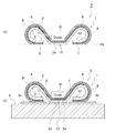
この実施の形態1に係る実装基板9は、図1(a)に示すように、略C字断面状の金属ベース回路基板1を有しており、金属ベース回路基板1の中央部13には、発熱素子として発光ダイオードDが実装されている。
As shown in FIG. 1A, the
この金属ベース回路基板1は、図1(a)に示すように、ベース金属2に絶縁層3を介して回路層4が積層され、さらに、回路層4の上側にレジスト8が積層された構造を有している。金属ベース回路基板1の両端部11、12は、それぞれ下側へベース金属2が内側となるように半円筒状に180°折り曲げられて、互いに同一の平面PL上に位置している。そして、この両端部11、12においては、図1(b)に示すように、金属ベース回路基板1が配線基板5に実装されたときに、回路層4が配線基板5の2本の回路配線5a、5bに電気的に接続されるように一対の電極6、7が露出している。
As shown in FIG. 1A, the metal
ここで、ベース金属2の材料としては、アルミニウム、アルミニウム合金、銅または銅合金などを用いることができ、熱伝導率が高いことから、銅または銅合金が好ましい。
Here, as a material of the
また、絶縁層3としては、樹脂を用いることができ、この樹脂としては、液晶ポリエステルが好ましいが、エポキシ樹脂でも構わない。これらの樹脂には、アルミナ、窒化ホウ素、窒化アルミニウム等の粒子を分散することが熱伝導率向上の点で好ましい。
Further, a resin can be used as the
さらに、回路層4の材料としては、銅または銅合金などを用いることができる。
Furthermore, as a material of the
そして、発光ダイオードDは、2つの電極が金属ベース回路基板1の回路層4に電気的に接続されている。
The light emitting diode D has two electrodes electrically connected to the
なお、この実装基板9を製造する方法としては、まず、平板状の金属ベース回路基板1を作製し、この金属ベース回路基板1の両端部11、12を折り曲げた後、この金属ベース回路基板1に発光ダイオードDを実装する方法が考えられる。
As a method of manufacturing the
実装基板9は以上のような構成を有するので、図1(b)に示すように、金属ベース回路基板1が配線基板5に実装されたときには、この金属ベース回路基板1の電極6、7がそれぞれ配線基板5の回路配線5a、5bに接触する。したがって、発光ダイオードDは、金属ベース回路基板1の回路層4を介して配線基板5の回路配線5a、5bと導通をとることができる。その結果、この金属ベース回路基板1は配線基板5に表面実装することが可能となる。
Since the
また、実装基板9は、図1(b)に示すように、金属ベース回路基板1が配線基板5に実装された状態では、発光ダイオードDは金属ベース回路基板1を介して配線基板5に接触している。そのため、発光ダイオードDで発生した熱は、金属ベース回路基板1を伝わって配線基板5へ放出される。したがって、この金属ベース回路基板1は、発光ダイオードDの放熱性にも優れたものとなる。
[発明の実施の形態2]
図2には、本発明の実施の形態2(金属ベース回路基板の回路層に発光ダイオードがフリップチップ実装された別の例)を示す。
Further, as shown in FIG. 1B, the
[
FIG. 2 shows a second embodiment of the present invention (another example in which a light emitting diode is flip-chip mounted on a circuit layer of a metal base circuit board).
この実施の形態2に係る実装基板9では、図2(a)に示すように、金属ベース回路基板1の中央部13がカップ状(台形断面状)に凹まされて形成され、金属ベース回路基板1の両端部11、12と同一の平面PL上に位置している。そのため、図2(b)に示すように、この金属ベース回路基板1が配線基板5に実装されたときには、ベース金属2の中央部2aと配線基板5との間に隙間がなく、ベース金属2の中央部2aが配線基板5のダミー配線5cに接触した状態になる。その他の構成については、上述した実施の形態1と同様であるので、同一の部材については、同一の符号を付してその説明を省略する。
In the
したがって、この実装基板9では、上述した実施の形態1と同じ作用効果を奏する。
Therefore, the
これに加えて、この実装基板9では、上述したとおり、金属ベース回路基板1が配線基板5に実装されたときに、この金属ベース回路基板1のベース金属2の中央部2aが配線基板5に接触した状態、つまり熱的に接地した状態になるので、発光ダイオードDで発生した熱は、ベース金属2の中央部2aから直ちに配線基板5へ放出される。したがって、発光ダイオードDの放熱性を一層向上させることができる。
In addition to this, in the
また、この実装基板9では、上述したとおり、金属ベース回路基板1の中央部13がカップ状に形成されているので、このカップ状の中央部13をリフレクターとして機能させ、発光ダイオードDから出射した光をカップ状の中央部13に反射させることにより、発光ダイオードDの指向性を高めることができる。
[発明の実施の形態3]
図3には、本発明の実施の形態3(金属ベース回路基板の回路層に発光ダイオードの2つの電極がワイヤー接続された一例)を示す。
Moreover, in this
FIG. 3 shows a third embodiment of the present invention (an example in which two electrodes of a light emitting diode are connected to a circuit layer of a metal base circuit board).
この実施の形態3に係る実装基板9では、図3に示すように、金属ベース回路基板1の中央部13において、絶縁層3および回路層4が部分的に剥離されて発光ダイオードDがベース金属2に載置され、この発光ダイオードDの2つの電極が2本のワイヤー15で金属ベース回路基板1の回路層4に電気的に接続されている。その他の構成については、上述した実施の形態1と同様であるので、同一の部材については、同一の符号を付してその説明を省略する。
In the mounting
したがって、この実装基板9では、上述した実施の形態1と比べて、発光ダイオードDがワイヤー15を介して回路層4に電気的に接続されている点で異なるが、実施の形態1と同じ作用効果を奏する。
[発明の実施の形態4]
図4には、本発明の実施の形態4(金属ベース回路基板の回路層に発光ダイオードの2つの電極がワイヤー接続された別の例)を示す。
Therefore, the mounting
[
FIG. 4 shows
この実施の形態4に係る実装基板9では、図4(a)に示すように、金属ベース回路基板1の中央部13がカップ状(台形断面状)に凹まされて形成され、金属ベース回路基板1の両端部11、12と同一の平面PL上に位置している。そのため、図4(b)に示すように、この金属ベース回路基板1が配線基板5に実装されたときには、ベース金属2の中央部2aと配線基板5との間に隙間がなく、ベース金属2の中央部2aが配線基板5のダミー配線5cに接触した状態になる。その他の構成については、上述した実施の形態3と同様であるので、同一の部材については、同一の符号を付してその説明を省略する。
In the mounting
したがって、この実装基板9では、上述した実施の形態3と同じ作用効果を奏する。
Therefore, the mounting
これに加えて、この実装基板9では、上述したとおり、金属ベース回路基板1が配線基板5に実装されたときに、この金属ベース回路基板1のベース金属2の中央部2aが配線基板5に接触した状態、つまり熱的に接地した状態になるので、発光ダイオードDで発生した熱は、ベース金属2の中央部2aから直ちに配線基板5へ放出される。したがって、発光ダイオードDの放熱性を一層向上させることができる。
[発明の実施の形態5]
図5には、本発明の実施の形態5(金属ベース回路基板の回路層に発光ダイオードの一方の電極がワイヤー接続されるとともに、金属ベース回路基板のベース金属に発光ダイオードの他方の電極が電気的に接続された一例)を示す。
In addition to this, in the mounting
FIG. 5 shows a fifth embodiment of the present invention (one electrode of a light emitting diode is wire-connected to a circuit layer of a metal base circuit board, and the other electrode of the light emitting diode is electrically connected to a base metal of the metal base circuit board. An example of a connected system).
この実施の形態5に係る実装基板9では、図5(a)に示すように、金属ベース回路基板1の載置部14が凹まされて形成され、金属ベース回路基板1の端部11と同一の平面PL上に位置している。また、図5に示すように、発光ダイオードDの一方の電極がワイヤー15で金属ベース回路基板1の回路層4に電気的に接続されているとともに、発光ダイオードDが金属ベース回路基板1の載置部14に実装されることにより、他方の電極が金属ベース回路基板1のベース金属2に電気的に接続されている。その他の構成については、上述した実施の形態4と同様であるので、同一の部材については、同一の符号を付してその説明を省略する。
In the mounting
したがって、この実装基板9では、上述した実施の形態4と同じ作用効果を奏する。
Therefore, the mounting
よって、この実装基板9では、金属ベース回路基板1の載置部14が凹まされて金属ベース回路基板1の端部11と同一の平面PL上に位置しており、かつ、発光ダイオードDの一方の電極がワイヤー15で金属ベース回路基板1の回路層4に電気的に接続されているとともに、発光ダイオードDの他方の電極が金属ベース回路基板1のベース金属2に電気的に接続されている。そのため、図5(b)に示すように、金属ベース回路基板1が配線基板5に実装されたときには、この金属ベース回路基板1の電極6が配線基板5の回路配線5aに接触するとともに、この金属ベース回路基板1のベース金属2の載置部2bが配線基板5の回路配線5bに接触する。したがって、発光ダイオードDは、金属ベース回路基板1の回路層4およびベース金属2を介して配線基板5の回路配線5a、5bと導通をとることができる。その結果、この金属ベース回路基板1は、上述した実施の形態1〜4と同様、配線基板5に表面実装することが可能となる。
Therefore, in this mounting
しかも、この実装基板9では、上述した実施の形態1〜4と比べて小型化が可能で、かつ、金属ベース回路基板1が配線基板5に実装されたとき、ベース金属2の載置部2bが配線基板5の回路配線5bに接触した状態となるので、発光ダイオードDで発生した熱は、ベース金属2の載置部2bを伝わって配線基板5へ迅速に放出される。その結果、発光ダイオードDの放熱性を一層向上させることができる。
[発明のその他の実施の形態]
なお、上述した実施の形態1〜4では、金属ベース回路基板1の両端部11、12が180°折り曲げられて、互いに同一の平面PL上に位置している場合について説明した。しかし、金属ベース回路基板1が配線基板5に実装されたときに、この配線基板5に回路層4が電気的に接続されるように電極6、7が露出している限り、金属ベース回路基板1の両端部11、12を必ずしも180°折り曲げる必要はなく、また、金属ベース回路基板1の両端部11、12を必ずしも同一の平面PL上に位置させる必要もない。
Moreover, the mounting
[Other Embodiments of the Invention]
In the first to fourth embodiments described above, the case where both end
また、上述した実施の形態5では、金属ベース回路基板1の端部11が180°折り曲げられるとともに、金属ベース回路基板1の載置部14が凹まされて金属ベース回路基板1の端部11と同一の平面PL上に位置している場合について説明した。しかし、金属ベース回路基板1が配線基板5に実装されたときに、この配線基板5に回路層4とベース金属2が電気的に接続されるように電極6とベース金属2が露出している限り、金属ベース回路基板1の端部11を必ずしも180°折り曲げる必要はなく、また、金属ベース回路基板1の端部11と載置部14を必ずしも同一の平面PL上に位置させる必要もない。
Further, in the fifth embodiment described above, the
また、上述した実施の形態2、4では、図2(b)および図4(b)に示すように、金属ベース回路基板1が配線基板5に実装されたときに、ベース金属2の中央部2aが配線基板5のダミー配線5cに接触する場合について説明した。ここで、金属ベース回路基板1が配線基板5に実装されたときに、ベース金属2の中央部2aが配線基板5のダミー配線5cとはんだで接続された状態になるように構成した場合が、熱伝導が良いため好ましく、発光ダイオードDの放熱性が一層向上する。
In the second and fourth embodiments described above, when the metal
また、上述した実施の形態2、4では、金属ベース回路基板1の中央部13がカップ状に形成されている場合について説明した。しかし、金属ベース回路基板1が配線基板5に実装されたときに、この配線基板5にベース金属2が接地または近接する限り、金属ベース回路基板1の中央部13を必ずしもカップ状に形成する必要はない。
In the second and fourth embodiments, the case where the
また、上述した実施の形態3では、図3に示すように、金属ベース回路基板1の中央部13において、絶縁層3および回路層4を部分的に剥離して発光ダイオードDをベース金属2に載置した場合について説明した。しかし、回路層4のみを部分的に剥離して発光ダイオードDを絶縁層3に載置することも可能である。
In the third embodiment described above, as shown in FIG. 3, the insulating
また、上述した実施の形態1〜5では、1個の発光ダイオードDを金属ベース回路基板1に実装する場合について説明した。しかし、複数個(2個以上)の発光ダイオードDが電気的に直列または並列に接続されたものを金属ベース回路基板1に実装する場合に本発明を同様に適用することもできる。
In the first to fifth embodiments, the case where one light-emitting diode D is mounted on the metal
さらに、上述した実施の形態1〜5では、発熱素子として発光ダイオードDを用いた場合について説明したが、発光ダイオードD以外の発熱素子(例えば、整流用ダイオード、トランジスタ、サイリスタなど)を実装する場合に本発明を同様に適用することも可能である。 Furthermore, in the first to fifth embodiments described above, the case where the light emitting diode D is used as the heat generating element has been described. It is also possible to apply the present invention to the above.
本発明は、液晶表示装置のバックライトの発光モジュールの構成部品その他に適用することができる。 The present invention can be applied to components and the like of a light emitting module of a backlight of a liquid crystal display device.
1……金属ベース回路基板
2……ベース金属
2a……中央部
2b……載置部
3……絶縁層
4……回路層
5……配線基板
5a、5b……回路配線
5c……ダミー配線
6、7……電極
8……レジスト
9……実装基板
11、12……端部
13……中央部
14……載置部
15……ワイヤー
D……発光ダイオード(発熱素子)
PL……平面
DESCRIPTION OF
PL …… Plane
Claims (6)
ベース金属に絶縁層を介して回路層が積層された構造を有し、
少なくとも一方の端部は、前記ベース金属が内側となるように折り曲げられ、前記配線基板に実装されたときに前記回路層が当該配線基板に電気的に接続されるように電極が露出していることを特徴とする金属ベース回路基板。 A metal base circuit board mounted on a wiring board,
It has a structure in which a circuit layer is laminated on an insulating layer on a base metal,
At least one end is bent so that the base metal is on the inside, and the electrode is exposed so that the circuit layer is electrically connected to the wiring board when mounted on the wiring board. A metal-based circuit board characterized by that.
ベース金属に絶縁層を介して回路層が積層された構造を有し、
両端部は、それぞれ前記ベース金属が内側となるように折り曲げられ、この両端部において、前記配線基板に実装されたときに前記回路層が当該配線基板に電気的に接続されるように一対の電極が露出していることを特徴とする金属ベース回路基板。 A metal base circuit board mounted on a wiring board,
It has a structure in which a circuit layer is laminated on an insulating layer on a base metal,
Both ends are bent so that the base metal is inside, and a pair of electrodes is provided at both ends so that the circuit layer is electrically connected to the wiring board when mounted on the wiring board. A metal-based circuit board characterized in that is exposed.
Priority Applications (1)
| Application Number | Priority Date | Filing Date | Title |
|---|---|---|---|
| JP2012216600A JP2014072331A (en) | 2012-09-28 | 2012-09-28 | Metal base circuit board and mounting substrate |
Applications Claiming Priority (1)
| Application Number | Priority Date | Filing Date | Title |
|---|---|---|---|
| JP2012216600A JP2014072331A (en) | 2012-09-28 | 2012-09-28 | Metal base circuit board and mounting substrate |
Publications (1)
| Publication Number | Publication Date |
|---|---|
| JP2014072331A true JP2014072331A (en) | 2014-04-21 |
Family
ID=50747290
Family Applications (1)
| Application Number | Title | Priority Date | Filing Date |
|---|---|---|---|
| JP2012216600A Pending JP2014072331A (en) | 2012-09-28 | 2012-09-28 | Metal base circuit board and mounting substrate |
Country Status (1)
| Country | Link |
|---|---|
| JP (1) | JP2014072331A (en) |
Cited By (2)
| Publication number | Priority date | Publication date | Assignee | Title |
|---|---|---|---|---|
| US20210106280A1 (en) * | 2018-02-27 | 2021-04-15 | Koninklijke Philips N.V. | Sensor arrangement for mounting on a guidewire or catheter |
| US11956894B2 (en) | 2019-03-05 | 2024-04-09 | Signify Holding, B.V. | Flexible printed circuit board assembly |
-
2012
- 2012-09-28 JP JP2012216600A patent/JP2014072331A/en active Pending
Cited By (2)
| Publication number | Priority date | Publication date | Assignee | Title |
|---|---|---|---|---|
| US20210106280A1 (en) * | 2018-02-27 | 2021-04-15 | Koninklijke Philips N.V. | Sensor arrangement for mounting on a guidewire or catheter |
| US11956894B2 (en) | 2019-03-05 | 2024-04-09 | Signify Holding, B.V. | Flexible printed circuit board assembly |
Similar Documents
| Publication | Publication Date | Title |
|---|---|---|
| JP5283750B2 (en) | Thermally conductive mounting elements for mounting printed circuit boards to heat sinks | |
| KR101134671B1 (en) | LED lamp module with the cooling structure | |
| KR101130137B1 (en) | Led module | |
| JP2009536453A (en) | Thermal surface mounting of multiple LEDs on a heat sink | |
| US7939919B2 (en) | LED-packaging arrangement and light bar employing the same | |
| JP6427313B2 (en) | Light emitting device | |
| US8801238B2 (en) | Light-emitting device | |
| US10236429B2 (en) | Mounting assembly and lighting device | |
| JP2009004129A (en) | Substrate, and illumination device | |
| US20160308106A1 (en) | Floating heat sink support with copper sheets and led package assembly for led flip chip package | |
| JP2017199842A (en) | LED light source device | |
| RU2008108713A (en) | MOUNTING PANEL FOR ELECTRONIC COMPONENT | |
| KR101115403B1 (en) | Light emitting apparatus | |
| JP2014072331A (en) | Metal base circuit board and mounting substrate | |
| JP5968647B2 (en) | LED lamp and LED lighting device | |
| KR101064013B1 (en) | Light emitting module | |
| US20140168979A1 (en) | Light emitting diode module with heat-conducting poles | |
| KR101507568B1 (en) | Heat sink | |
| CN209071380U (en) | It is a kind of for assembling the circuit substrate of light emitting diode | |
| KR101259876B1 (en) | Led package having a thermoelectric element and method for manufacturin thereof | |
| JP2010287749A (en) | Light emitting body and lighting instrument | |
| WO2011155340A1 (en) | Flexible printed wiring board | |
| KR101138442B1 (en) | Light emitting device | |
| JP2012018881A (en) | Lighting fixture | |
| KR101348484B1 (en) | Led package and method for manufacturing the same |