EP3083254B1 - Laser printing system - Google Patents
Laser printing system Download PDFInfo
- Publication number
- EP3083254B1 EP3083254B1 EP14812255.9A EP14812255A EP3083254B1 EP 3083254 B1 EP3083254 B1 EP 3083254B1 EP 14812255 A EP14812255 A EP 14812255A EP 3083254 B1 EP3083254 B1 EP 3083254B1
- Authority
- EP
- European Patent Office
- Prior art keywords
- laser
- arrays
- printing system
- working plane
- module
- Prior art date
- Legal status (The legal status is an assumption and is not a legal conclusion. Google has not performed a legal analysis and makes no representation as to the accuracy of the status listed.)
- Active
Links
- 238000007648 laser printing Methods 0.000 title claims description 70
- 238000003491 array Methods 0.000 claims description 103
- 239000004065 semiconductor Substances 0.000 claims description 73
- 230000003287 optical effect Effects 0.000 claims description 57
- 238000000034 method Methods 0.000 claims description 21
- 238000003384 imaging method Methods 0.000 claims description 18
- 238000005286 illumination Methods 0.000 claims description 17
- 238000007639 printing Methods 0.000 description 22
- 238000009826 distribution Methods 0.000 description 10
- 230000001681 protective effect Effects 0.000 description 7
- 238000010146 3D printing Methods 0.000 description 5
- 230000001419 dependent effect Effects 0.000 description 4
- 238000010438 heat treatment Methods 0.000 description 4
- 230000007257 malfunction Effects 0.000 description 4
- 239000004566 building material Substances 0.000 description 3
- 238000013461 design Methods 0.000 description 3
- 239000000758 substrate Substances 0.000 description 3
- 230000007547 defect Effects 0.000 description 2
- 239000011521 glass Substances 0.000 description 2
- 238000004519 manufacturing process Methods 0.000 description 2
- 239000000463 material Substances 0.000 description 2
- 238000002844 melting Methods 0.000 description 2
- 230000008018 melting Effects 0.000 description 2
- 230000008569 process Effects 0.000 description 2
- 238000012545 processing Methods 0.000 description 2
- 230000005855 radiation Effects 0.000 description 2
- 238000010521 absorption reaction Methods 0.000 description 1
- 239000000654 additive Substances 0.000 description 1
- 230000000996 additive effect Effects 0.000 description 1
- 238000013459 approach Methods 0.000 description 1
- 201000009310 astigmatism Diseases 0.000 description 1
- 230000008901 benefit Effects 0.000 description 1
- 230000008859 change Effects 0.000 description 1
- 229910003460 diamond Inorganic materials 0.000 description 1
- 239000010432 diamond Substances 0.000 description 1
- 230000002708 enhancing effect Effects 0.000 description 1
- 230000006872 improvement Effects 0.000 description 1
- 230000004048 modification Effects 0.000 description 1
- 238000012986 modification Methods 0.000 description 1
- 238000000465 moulding Methods 0.000 description 1
- 239000000843 powder Substances 0.000 description 1
- 230000009467 reduction Effects 0.000 description 1
- 230000011218 segmentation Effects 0.000 description 1
- 238000005245 sintering Methods 0.000 description 1
- 238000004513 sizing Methods 0.000 description 1
- 230000007704 transition Effects 0.000 description 1
Images


Classifications
-
- B—PERFORMING OPERATIONS; TRANSPORTING
- B29—WORKING OF PLASTICS; WORKING OF SUBSTANCES IN A PLASTIC STATE IN GENERAL
- B29C—SHAPING OR JOINING OF PLASTICS; SHAPING OF MATERIAL IN A PLASTIC STATE, NOT OTHERWISE PROVIDED FOR; AFTER-TREATMENT OF THE SHAPED PRODUCTS, e.g. REPAIRING
- B29C64/00—Additive manufacturing, i.e. manufacturing of three-dimensional [3D] objects by additive deposition, additive agglomeration or additive layering, e.g. by 3D printing, stereolithography or selective laser sintering
- B29C64/10—Processes of additive manufacturing
- B29C64/141—Processes of additive manufacturing using only solid materials
- B29C64/153—Processes of additive manufacturing using only solid materials using layers of powder being selectively joined, e.g. by selective laser sintering or melting
-
- B—PERFORMING OPERATIONS; TRANSPORTING
- B41—PRINTING; LINING MACHINES; TYPEWRITERS; STAMPS
- B41J—TYPEWRITERS; SELECTIVE PRINTING MECHANISMS, i.e. MECHANISMS PRINTING OTHERWISE THAN FROM A FORME; CORRECTION OF TYPOGRAPHICAL ERRORS
- B41J2/00—Typewriters or selective printing mechanisms characterised by the printing or marking process for which they are designed
- B41J2/435—Typewriters or selective printing mechanisms characterised by the printing or marking process for which they are designed characterised by selective application of radiation to a printing material or impression-transfer material
- B41J2/447—Typewriters or selective printing mechanisms characterised by the printing or marking process for which they are designed characterised by selective application of radiation to a printing material or impression-transfer material using arrays of radiation sources
- B41J2/45—Typewriters or selective printing mechanisms characterised by the printing or marking process for which they are designed characterised by selective application of radiation to a printing material or impression-transfer material using arrays of radiation sources using light-emitting diode [LED] or laser arrays
-
- B—PERFORMING OPERATIONS; TRANSPORTING
- B22—CASTING; POWDER METALLURGY
- B22F—WORKING METALLIC POWDER; MANUFACTURE OF ARTICLES FROM METALLIC POWDER; MAKING METALLIC POWDER; APPARATUS OR DEVICES SPECIALLY ADAPTED FOR METALLIC POWDER
- B22F12/00—Apparatus or devices specially adapted for additive manufacturing; Auxiliary means for additive manufacturing; Combinations of additive manufacturing apparatus or devices with other processing apparatus or devices
- B22F12/38—Housings, e.g. machine housings
-
- B—PERFORMING OPERATIONS; TRANSPORTING
- B22—CASTING; POWDER METALLURGY
- B22F—WORKING METALLIC POWDER; MANUFACTURE OF ARTICLES FROM METALLIC POWDER; MAKING METALLIC POWDER; APPARATUS OR DEVICES SPECIALLY ADAPTED FOR METALLIC POWDER
- B22F12/00—Apparatus or devices specially adapted for additive manufacturing; Auxiliary means for additive manufacturing; Combinations of additive manufacturing apparatus or devices with other processing apparatus or devices
- B22F12/40—Radiation means
- B22F12/41—Radiation means characterised by the type, e.g. laser or electron beam
- B22F12/42—Light-emitting diodes [LED]
-
- B—PERFORMING OPERATIONS; TRANSPORTING
- B22—CASTING; POWDER METALLURGY
- B22F—WORKING METALLIC POWDER; MANUFACTURE OF ARTICLES FROM METALLIC POWDER; MAKING METALLIC POWDER; APPARATUS OR DEVICES SPECIALLY ADAPTED FOR METALLIC POWDER
- B22F12/00—Apparatus or devices specially adapted for additive manufacturing; Auxiliary means for additive manufacturing; Combinations of additive manufacturing apparatus or devices with other processing apparatus or devices
- B22F12/40—Radiation means
- B22F12/44—Radiation means characterised by the configuration of the radiation means
- B22F12/45—Two or more
-
- B—PERFORMING OPERATIONS; TRANSPORTING
- B22—CASTING; POWDER METALLURGY
- B22F—WORKING METALLIC POWDER; MANUFACTURE OF ARTICLES FROM METALLIC POWDER; MAKING METALLIC POWDER; APPARATUS OR DEVICES SPECIALLY ADAPTED FOR METALLIC POWDER
- B22F12/00—Apparatus or devices specially adapted for additive manufacturing; Auxiliary means for additive manufacturing; Combinations of additive manufacturing apparatus or devices with other processing apparatus or devices
- B22F12/40—Radiation means
- B22F12/46—Radiation means with translatory movement
- B22F12/47—Radiation means with translatory movement parallel to the deposition plane
-
- B—PERFORMING OPERATIONS; TRANSPORTING
- B22—CASTING; POWDER METALLURGY
- B22F—WORKING METALLIC POWDER; MANUFACTURE OF ARTICLES FROM METALLIC POWDER; MAKING METALLIC POWDER; APPARATUS OR DEVICES SPECIALLY ADAPTED FOR METALLIC POWDER
- B22F12/00—Apparatus or devices specially adapted for additive manufacturing; Auxiliary means for additive manufacturing; Combinations of additive manufacturing apparatus or devices with other processing apparatus or devices
- B22F12/40—Radiation means
- B22F12/49—Scanners
-
- B—PERFORMING OPERATIONS; TRANSPORTING
- B23—MACHINE TOOLS; METAL-WORKING NOT OTHERWISE PROVIDED FOR
- B23K—SOLDERING OR UNSOLDERING; WELDING; CLADDING OR PLATING BY SOLDERING OR WELDING; CUTTING BY APPLYING HEAT LOCALLY, e.g. FLAME CUTTING; WORKING BY LASER BEAM
- B23K26/00—Working by laser beam, e.g. welding, cutting or boring
- B23K26/02—Positioning or observing the workpiece, e.g. with respect to the point of impact; Aligning, aiming or focusing the laser beam
- B23K26/06—Shaping the laser beam, e.g. by masks or multi-focusing
- B23K26/064—Shaping the laser beam, e.g. by masks or multi-focusing by means of optical elements, e.g. lenses, mirrors or prisms
-
- B—PERFORMING OPERATIONS; TRANSPORTING
- B23—MACHINE TOOLS; METAL-WORKING NOT OTHERWISE PROVIDED FOR
- B23K—SOLDERING OR UNSOLDERING; WELDING; CLADDING OR PLATING BY SOLDERING OR WELDING; CUTTING BY APPLYING HEAT LOCALLY, e.g. FLAME CUTTING; WORKING BY LASER BEAM
- B23K26/00—Working by laser beam, e.g. welding, cutting or boring
- B23K26/08—Devices involving relative movement between laser beam and workpiece
- B23K26/083—Devices involving movement of the workpiece in at least one axial direction
- B23K26/0853—Devices involving movement of the workpiece in at least in two axial directions, e.g. in a plane
-
- B—PERFORMING OPERATIONS; TRANSPORTING
- B23—MACHINE TOOLS; METAL-WORKING NOT OTHERWISE PROVIDED FOR
- B23K—SOLDERING OR UNSOLDERING; WELDING; CLADDING OR PLATING BY SOLDERING OR WELDING; CUTTING BY APPLYING HEAT LOCALLY, e.g. FLAME CUTTING; WORKING BY LASER BEAM
- B23K26/00—Working by laser beam, e.g. welding, cutting or boring
- B23K26/34—Laser welding for purposes other than joining
- B23K26/342—Build-up welding
-
- B—PERFORMING OPERATIONS; TRANSPORTING
- B29—WORKING OF PLASTICS; WORKING OF SUBSTANCES IN A PLASTIC STATE IN GENERAL
- B29C—SHAPING OR JOINING OF PLASTICS; SHAPING OF MATERIAL IN A PLASTIC STATE, NOT OTHERWISE PROVIDED FOR; AFTER-TREATMENT OF THE SHAPED PRODUCTS, e.g. REPAIRING
- B29C64/00—Additive manufacturing, i.e. manufacturing of three-dimensional [3D] objects by additive deposition, additive agglomeration or additive layering, e.g. by 3D printing, stereolithography or selective laser sintering
- B29C64/20—Apparatus for additive manufacturing; Details thereof or accessories therefor
- B29C64/25—Housings, e.g. machine housings
-
- B—PERFORMING OPERATIONS; TRANSPORTING
- B29—WORKING OF PLASTICS; WORKING OF SUBSTANCES IN A PLASTIC STATE IN GENERAL
- B29C—SHAPING OR JOINING OF PLASTICS; SHAPING OF MATERIAL IN A PLASTIC STATE, NOT OTHERWISE PROVIDED FOR; AFTER-TREATMENT OF THE SHAPED PRODUCTS, e.g. REPAIRING
- B29C64/00—Additive manufacturing, i.e. manufacturing of three-dimensional [3D] objects by additive deposition, additive agglomeration or additive layering, e.g. by 3D printing, stereolithography or selective laser sintering
- B29C64/20—Apparatus for additive manufacturing; Details thereof or accessories therefor
- B29C64/264—Arrangements for irradiation
- B29C64/268—Arrangements for irradiation using laser beams; using electron beams [EB]
-
- B—PERFORMING OPERATIONS; TRANSPORTING
- B29—WORKING OF PLASTICS; WORKING OF SUBSTANCES IN A PLASTIC STATE IN GENERAL
- B29C—SHAPING OR JOINING OF PLASTICS; SHAPING OF MATERIAL IN A PLASTIC STATE, NOT OTHERWISE PROVIDED FOR; AFTER-TREATMENT OF THE SHAPED PRODUCTS, e.g. REPAIRING
- B29C64/00—Additive manufacturing, i.e. manufacturing of three-dimensional [3D] objects by additive deposition, additive agglomeration or additive layering, e.g. by 3D printing, stereolithography or selective laser sintering
- B29C64/20—Apparatus for additive manufacturing; Details thereof or accessories therefor
- B29C64/264—Arrangements for irradiation
- B29C64/277—Arrangements for irradiation using multiple radiation means, e.g. micromirrors or multiple light-emitting diodes [LED]
- B29C64/282—Arrangements for irradiation using multiple radiation means, e.g. micromirrors or multiple light-emitting diodes [LED] of the same type, e.g. using different energy levels
-
- B—PERFORMING OPERATIONS; TRANSPORTING
- B29—WORKING OF PLASTICS; WORKING OF SUBSTANCES IN A PLASTIC STATE IN GENERAL
- B29C—SHAPING OR JOINING OF PLASTICS; SHAPING OF MATERIAL IN A PLASTIC STATE, NOT OTHERWISE PROVIDED FOR; AFTER-TREATMENT OF THE SHAPED PRODUCTS, e.g. REPAIRING
- B29C64/00—Additive manufacturing, i.e. manufacturing of three-dimensional [3D] objects by additive deposition, additive agglomeration or additive layering, e.g. by 3D printing, stereolithography or selective laser sintering
- B29C64/30—Auxiliary operations or equipment
- B29C64/386—Data acquisition or data processing for additive manufacturing
- B29C64/393—Data acquisition or data processing for additive manufacturing for controlling or regulating additive manufacturing processes
-
- B—PERFORMING OPERATIONS; TRANSPORTING
- B33—ADDITIVE MANUFACTURING TECHNOLOGY
- B33Y—ADDITIVE MANUFACTURING, i.e. MANUFACTURING OF THREE-DIMENSIONAL [3-D] OBJECTS BY ADDITIVE DEPOSITION, ADDITIVE AGGLOMERATION OR ADDITIVE LAYERING, e.g. BY 3-D PRINTING, STEREOLITHOGRAPHY OR SELECTIVE LASER SINTERING
- B33Y10/00—Processes of additive manufacturing
-
- B—PERFORMING OPERATIONS; TRANSPORTING
- B33—ADDITIVE MANUFACTURING TECHNOLOGY
- B33Y—ADDITIVE MANUFACTURING, i.e. MANUFACTURING OF THREE-DIMENSIONAL [3-D] OBJECTS BY ADDITIVE DEPOSITION, ADDITIVE AGGLOMERATION OR ADDITIVE LAYERING, e.g. BY 3-D PRINTING, STEREOLITHOGRAPHY OR SELECTIVE LASER SINTERING
- B33Y30/00—Apparatus for additive manufacturing; Details thereof or accessories therefor
-
- B—PERFORMING OPERATIONS; TRANSPORTING
- B33—ADDITIVE MANUFACTURING TECHNOLOGY
- B33Y—ADDITIVE MANUFACTURING, i.e. MANUFACTURING OF THREE-DIMENSIONAL [3-D] OBJECTS BY ADDITIVE DEPOSITION, ADDITIVE AGGLOMERATION OR ADDITIVE LAYERING, e.g. BY 3-D PRINTING, STEREOLITHOGRAPHY OR SELECTIVE LASER SINTERING
- B33Y50/00—Data acquisition or data processing for additive manufacturing
- B33Y50/02—Data acquisition or data processing for additive manufacturing for controlling or regulating additive manufacturing processes
-
- B—PERFORMING OPERATIONS; TRANSPORTING
- B41—PRINTING; LINING MACHINES; TYPEWRITERS; STAMPS
- B41J—TYPEWRITERS; SELECTIVE PRINTING MECHANISMS, i.e. MECHANISMS PRINTING OTHERWISE THAN FROM A FORME; CORRECTION OF TYPOGRAPHICAL ERRORS
- B41J2/00—Typewriters or selective printing mechanisms characterised by the printing or marking process for which they are designed
- B41J2/435—Typewriters or selective printing mechanisms characterised by the printing or marking process for which they are designed characterised by selective application of radiation to a printing material or impression-transfer material
- B41J2/447—Typewriters or selective printing mechanisms characterised by the printing or marking process for which they are designed characterised by selective application of radiation to a printing material or impression-transfer material using arrays of radiation sources
- B41J2/45—Typewriters or selective printing mechanisms characterised by the printing or marking process for which they are designed characterised by selective application of radiation to a printing material or impression-transfer material using arrays of radiation sources using light-emitting diode [LED] or laser arrays
- B41J2/451—Special optical means therefor, e.g. lenses, mirrors, focusing means
-
- B—PERFORMING OPERATIONS; TRANSPORTING
- B41—PRINTING; LINING MACHINES; TYPEWRITERS; STAMPS
- B41J—TYPEWRITERS; SELECTIVE PRINTING MECHANISMS, i.e. MECHANISMS PRINTING OTHERWISE THAN FROM A FORME; CORRECTION OF TYPOGRAPHICAL ERRORS
- B41J2/00—Typewriters or selective printing mechanisms characterised by the printing or marking process for which they are designed
- B41J2/435—Typewriters or selective printing mechanisms characterised by the printing or marking process for which they are designed characterised by selective application of radiation to a printing material or impression-transfer material
- B41J2/447—Typewriters or selective printing mechanisms characterised by the printing or marking process for which they are designed characterised by selective application of radiation to a printing material or impression-transfer material using arrays of radiation sources
- B41J2/455—Typewriters or selective printing mechanisms characterised by the printing or marking process for which they are designed characterised by selective application of radiation to a printing material or impression-transfer material using arrays of radiation sources using laser arrays, the laser array being smaller than the medium to be recorded
-
- G—PHYSICS
- G02—OPTICS
- G02B—OPTICAL ELEMENTS, SYSTEMS OR APPARATUS
- G02B3/00—Simple or compound lenses
- G02B3/0006—Arrays
-
- H—ELECTRICITY
- H01—ELECTRIC ELEMENTS
- H01S—DEVICES USING THE PROCESS OF LIGHT AMPLIFICATION BY STIMULATED EMISSION OF RADIATION [LASER] TO AMPLIFY OR GENERATE LIGHT; DEVICES USING STIMULATED EMISSION OF ELECTROMAGNETIC RADIATION IN WAVE RANGES OTHER THAN OPTICAL
- H01S5/00—Semiconductor lasers
- H01S5/005—Optical components external to the laser cavity, specially adapted therefor, e.g. for homogenisation or merging of the beams or for manipulating laser pulses, e.g. pulse shaping
- H01S5/0071—Optical components external to the laser cavity, specially adapted therefor, e.g. for homogenisation or merging of the beams or for manipulating laser pulses, e.g. pulse shaping for beam steering, e.g. using a mirror outside the cavity to change the beam direction
-
- H—ELECTRICITY
- H01—ELECTRIC ELEMENTS
- H01S—DEVICES USING THE PROCESS OF LIGHT AMPLIFICATION BY STIMULATED EMISSION OF RADIATION [LASER] TO AMPLIFY OR GENERATE LIGHT; DEVICES USING STIMULATED EMISSION OF ELECTROMAGNETIC RADIATION IN WAVE RANGES OTHER THAN OPTICAL
- H01S5/00—Semiconductor lasers
- H01S5/40—Arrangement of two or more semiconductor lasers, not provided for in groups H01S5/02 - H01S5/30
- H01S5/42—Arrays of surface emitting lasers
- H01S5/423—Arrays of surface emitting lasers having a vertical cavity
-
- B—PERFORMING OPERATIONS; TRANSPORTING
- B22—CASTING; POWDER METALLURGY
- B22F—WORKING METALLIC POWDER; MANUFACTURE OF ARTICLES FROM METALLIC POWDER; MAKING METALLIC POWDER; APPARATUS OR DEVICES SPECIALLY ADAPTED FOR METALLIC POWDER
- B22F10/00—Additive manufacturing of workpieces or articles from metallic powder
- B22F10/20—Direct sintering or melting
- B22F10/28—Powder bed fusion, e.g. selective laser melting [SLM] or electron beam melting [EBM]
-
- G—PHYSICS
- G03—PHOTOGRAPHY; CINEMATOGRAPHY; ANALOGOUS TECHNIQUES USING WAVES OTHER THAN OPTICAL WAVES; ELECTROGRAPHY; HOLOGRAPHY
- G03G—ELECTROGRAPHY; ELECTROPHOTOGRAPHY; MAGNETOGRAPHY
- G03G15/00—Apparatus for electrographic processes using a charge pattern
- G03G15/22—Apparatus for electrographic processes using a charge pattern involving the combination of more than one step according to groups G03G13/02 - G03G13/20
- G03G15/225—Apparatus for electrographic processes using a charge pattern involving the combination of more than one step according to groups G03G13/02 - G03G13/20 using contact-printing
Definitions
- the invention relates to a laser printing system and a method of laser printing.
- Laser printing refers to printing of documents as well as 3D printing by means of lasers for additive manufacturing, for example, used for rapid prototyping.
- Conventional laser printers and selective-laser melting machines consist of a single high-power laser and a scanner to scan the laser over the area to be illuminated.
- a printing head with several independent channels i.e. an addressable array of lasers covering a significant part of the area.
- the printing head covers the full width of the area to be printed with one addressable laser source per pixel, so that the print head needs to be moved only in one direction. Reliability and service costs of such addressable arrays may be an issue.
- US 2005/0151828 A1 discloses a device for xerographic laser printing.
- the xerographic printing system has a laser printbar imager assembly including a plurality of micro-optic light emitting arrays.
- the micro-optic light emitting array includes a plurality of vertical cavity surface emitting lasers, where each vertical cavity surface emitting laser is focused with a micro-optic element.
- EP 124103A1 discloses a laser printing system according to the preamble of claim 1, and discloses a device for recording images on a printing form, including an array of light sources and imaging optics for generating imaging spots on a printing form, which is distinguished by the array of light sources including an array of mutually independently controllable VCSEL light sources.
- One specific imaging spot may be formed on the printing form by combining the light emitted by a subarray of the VCSEL light sources. Due to the advantageous beam properties of VCSEL light sources, such as the small divergence and negligible astigmatism, the device for recording images on printing forms is especially advantageous for use in a printing-form imaging unit or in a print unit.
- US5793783A discloses a method of producing a high power and brightness beam from diode laser source that either has a single emitting element or array with a plurality of segments or emitters that are concurrently addressable or has a plurality of elements or subarrays each having a plurality of laser segments or emitters, which elements or subarrays are independently addressable relative to one another.
- Beam filling and focusing optics are disposed in front of the emitters so that light from the individual emitters from each subarray converge to from a single overlapping spot.
- Segmentation of laser subarrays and emitters improves laser life by reducing thermal gradients and isolating any local failures to a single segment emitters while the focusing of the segments or emitters to overlapping light spots increases the tolerance of the source to local failures. Two or more emitters in a given element must fail before the source is considered to have failed.
- WO2011021140 discloses a laser device comprising an array of several large area VCSELs (101) and one or several optics (201, 202) designed and arranged to image the active layers of the VCSELs (101) of said array to a working plane (501) such that the laser radiation emitted by the active layers of all VCSELs (101) or of subgroups of VCSELs (101) of the array superimposes in the working plane (501).
- the proposed laser device allows the generation of a desired intensity distribution in the working plane without the need of an optics specially designed for this intensity distribution or beam profile.
- US20020140918A1 discloses down sizing of an image writing device by reducing a conjugate distance. A diameter of a spot light impinging on a photosensitive drum for illumination can be freely varied.
- the image writing device is equipped with a light source means having a light emission layer formed on a transparent substrate and a microlens array configured so as to face the light source.
- US2012/0188327A1 discloses an exposure device including a plurality of light emitting elements provided on a substrate, a plurality of hologram elements multiplexing-recorded in correspondence with the plurality of light emitting elements, respectively, such that, when the plurality of light emitting elements are made to emit light in the recording layer arranged on the substrate, a plurality of condensing points having light components emitted from two or more light emitting elements and condensed on one point, is formed, and a condensing point row extending in a predetermined direction is formed on the face to be exposed, and a driving unit that drives the plurality of light emitting elements, respectively.
- a laser printing system comprises at least two laser arrays of semiconductor lasers and at least one optical element.
- the optical element is adapted to image laser light emitted by the laser arrays, such that laser light of semiconductor lasers of one laser array is imaged to one pixel in a working plane of the laser printing system and an area element of the pixel is illuminated by means of at least two semiconductor lasers.
- CMOS complementary metal-oxide-semiconductor
- CMOS complementary metal-oxide-semiconductor
- VCSEL Vertical Cavity Surface Emitting Lasers
- VCSEL arrays can be easily manufactured in wafer based processes but usually emit less power as edge emitting semiconductor lasers.
- the optical systems of these known laser printing systems project or focus the light emitting layer of each semiconductor laser to the working plane.
- the present invention proposes to image at least two laser arrays to two pixels in the working plane by means of an optical element.
- the image of the laser arrays does not comprise sharp images of the light emitting layers of the semiconductor lasers.
- Light emitted by means of at least two lasers of one of the laser arrays illuminate each area element of the pixel such that there is no area element which is only illuminated by means of one single semiconductor laser.
- three, four or a multitude of semiconductor lasers of one laser array illuminate one area element of a pixel at the same time. It may even be that two laser arrays are imaged to the same pixel at the same time. More intensity can thus be provided to the working plane by using a multitude of semiconductor lasers per area element of a pixel.
- a diffuse image of a multitude of semiconductor lasers of the arrays form the pixels in the working plane.
- the laser printing system may be more reliable due to the relative low contribution of each single semiconductor laser to the illumination or energy input to an object in the working plane by means of optical energy.
- a malfunction of a single semiconductor laser of a laser array does consequently not cause a malfunction of the laser printing system.
- the wavelength of the emitted laser light is adapted to the absorption of the object in the working plane.
- the laser module may move relative to the laser printing system (scanning) and/or the object may move relative to the laser printing system.
- the object may be a sheet of paper, a powder layer which can be sintered by means of laser printing system or any other object which can be processed by means of the laser printing system. It may be preferred that only the object is moved.
- the laser printing system may be enabled to illuminate the full width of the object moving perpendicular to the width of the object by means of one, two, three, four or more laser modules.
- the semiconductor lasers may be edge emitting semiconductor lasers but VCSEL arrays may be preferred due to lower costs.
- the optical element is arranged in a way that an object plane of the optical element with respect to the working plane does not coincide with a plane of the semiconductor lasers such that the cones of laser light emitted by adjacent semiconductor lasers overlap in the object plane.
- the plane of the semiconductor lasers of the laser arrays is defined by means of the light emitting layers of the semiconductor lasers.
- the light emitting layers comprise the optical cavity of the semiconductor lasers comprising the active layer and the corresponding resonator mirrors.
- the optical element may be a single imaging lens or a more complex imaging optic defining an object plane relative to the working plane.
- the arrangement of the object plane with respect to the light emitting layers of the semiconductor lasers of the laser arrays may cause a diffuse overlapping image of the light emitting layers in the working plane.
- the energy distribution in the working plane may thus be more homogeneous in comparison to a projection of each light emitting layer of the semiconductor layers to the working plane.
- the optical element may be as simple as one projection lens per laser module but more complex combinations of lenses may be used in order to increase the distance between the working plane and the laser modules. No microlens arrays may be needed in order to provide a sharp projection of each light emitting layer.
- the laser module or laser modules of the laser printing system preferably comprises three, four or a multitude of laser arrays.
- a single laser array may be imaged to one pixel in the working plane.
- the pixel may be adjacent to each other such that a part of the emitted optical power of one laser array overlaps with the optical power emitted by another laser array. It may even be that two three or more laser arrays may be mapped to the same pixel in the working plane.
- the optical element may comprise an array of micro-optical elements which may image, for example, laser light of two, for example, adjacent arrays of the laser module to one pixel in the working plane. Two or more arrays may in this case be imaged to one pixel.
- laser light emitted by different laser arrays may illuminate the same part of a surface of an object at different times.
- the latter means that light of a first array may illuminate a defined surface of the object at a time t 1 and light of a second array may illuminate the defined surface of the object at a time t 2 later t 1 wherein the object was moved relative to the laser module(s).
- the printing system may comprise laser modules with different working planes. The latter may be done by placing laser modules at different heights relative to a reference surface and/or by providing different optical elements. Different working planes may be advantageous for three dimensional printing.
- the laser module(s) can be moved with respect to the reference surface being parallel to the working planes being always at a defined distance with respect to the laser modules.
- the laser arrays of the laser module or laser modules may be arranged in columns perpendicular to a direction of movement of the object in the working plane.
- the columns may be staggered or cascaded with respect to each other such that a first laser array of a first column of laser arrays is adapted to illuminate a first area of the object and a second laser array of a second column of laser arrays is adapted to illuminate a second area of the object, wherein the first area is adjacent to the second area such that continuous illumination of the object is enabled.
- the images of the laser arrays may partly overlap as discussed above.
- the laser arrays may be rectangular with the long side of the rectangle being arranged parallel to a direction of movement of the object in the working plane. This arrangement allows higher total powers per pixel by providing more semiconductor lasers per pixel, without reducing the resolution in the lateral direction perpendicular to the direction of movement of the object.
- the laser printing system may comprise two, three, four or a multitude of laser modules. Using a multitude of laser modules may enable a larger printing area. Furthermore, complex optical elements may be avoided by using, for example, one imaging lens per laser module.
- the laser modules may be arranged in columns perpendicular to a direction of movement of the object in the working plane.
- the columns may be staggered or cascaded with respect to each other such that a first laser module of a first column of laser modules is adapted to illuminate a first area of the object and a second laser module of a second column of laser modules is adapted to illuminate a second area of the object, wherein the first area is adjacent to the second area such that continuous illumination of the object is enabled.
- the number of columns of laser modules may be arranged in a way that the distance between laser modules in one column of laser modules is minimized.
- the module diameter and the width of the image of the arrays may determine the number of columns needed in order to enable an area covering illumination of the object by means of the laser modules. The bigger the diameter of the module in relation to the width of the image of the array arrangement the more columns may be needed.
- each laser module may be arranged in an elongated arrangement with the long side of the elongated arrangement being arranged perpendicular to the direction of movement of the object in the working plane.
- Each laser module may comprise, for example two, three or more columns of laser arrays perpendicular to the direction of movement of the object in the working plane. The number of arrays per column may surpass the number of columns.
- This arrangement may enable a homogeneous illumination of the object by means of a relatively simple driving scheme of the single arrays especially if more than one laser module is comprised by the laser printing system.
- Each area element of the object may in this case only be illuminated by one dedicated laser array wherein adjacent laser arrays illuminate adjacent pixels.
- the velocity of movement of the object in the working plane may be adapted in order to define the total energy per area element of the object.
- the laser printing system may comprise two, three, four or a multitude of laser modules wherein the laser arrays of each laser module are arranged in an elongated arrangement in order to enable a broad workspace (printing width perpendicular to the direction of movement of the object) of the laser printing system.
- the laser arrays of each laser module may alternatively be arranged in an elongated arrangement with the long side of the elongated arrangement being arranged slanted or rotated with respect to the direction being perpendicular to the direction of movement of the object in the working plane.
- a defined slanting angle or rotation of the elongated arrangement of laser modules around their centers may enable integrated intensity profiles with smooth slopes, which may also overlap with the adjacent pixels, to improve the homogeneity of the total intensity distribution, especially if the pixels are slightly misaligned with respect to each other. The latter reduces the alignment effort of the laser arrays and thus the manufacturing costs of the laser modules and the laser printing system.
- the misalignment may in extreme cases be compensated by an additional calibration run of the laser printing system in which the velocity of movement of the object in relation to the energy input per time and area element of a calibration object is determined.
- two, three or more laser arrays of the same laser module or different laser modules may be arranged to illuminate the same area element of the object.
- the laser arrays may be arranged to subsequently illuminate the area element.
- the energy input per time to an area element of the object in the working plane may be increased. This may enable higher velocities of the object and thus higher throughput of the laser printing system.
- the tolerance regarding misalignment of laser arrays and malfunctions of single semiconductor lasers may be improved.
- the driving schemes of different arrays may be adapted based on calibration runs with calibration objects as described above.
- the optical element of the laser modules may be arranged to demagnify the image of the laser arrays in the working plane.
- the demagnification may enable a smaller pixel size and higher energy densities.
- Each laser array may further comprises a micro-lens array being part of the optical element, the micro-lens array may be arranged to lower the divergence of the laser light emitted by the semiconductor lasers. The reduction of the divergence may be used to find compromise between the overlap of the laser light emitted by the semiconductor lasers in the object plane and the size of the single pixel.
- the distance between the laser array and the working plane may be adapted by means of the micro-lens array and/or the optical element (imaging optic) may be simplified.
- the density of laser arrays may change in dependence of an area of the object to be illuminated by means of the laser printing system. The latter may enable higher power densities at defined parts of the object.
- the density of the semiconductor lasers within the arrays may be adapted such that, for example, less or more intensity may be provided at the rim of the pixels.
- the shape of the arrays may be tailored in order to improve the homogeneity and/or to create a defined intensity distribution in the working plane.
- the arrays may, for example, have a diamond, triangle, round, elliptical, trapezoid or parallelogram shape.
- the laser printing system may comprise at least a first and a second laser module arranged next to each other.
- Each laser module comprises at least two laser arrays, wherein at least one of the two laser arrays of the first or the second laser module is arranged as an overlap laser light source such that in operation the same area element in the working plane can be illuminated by the overlap laser light source and a laser array of the laser module arranged next to the laser module comprising the overlap laser light source.
- the overlap laser light source is arranged to compensate potential misalignments of the laser modules which may result in unintended illumination gaps on the object in the working plane. Therefore the overlap may be partially.
- the laser arrays illuminate each one pixel in the working plane.
- the laser array which is arranged as overlap laser light source may be arranged to illuminate the same pixel or a part of the same pixel as the laser array of the neighboring laser module. This means that both laser arrays can illuminate the same area element in the working plane at the same moment in time.
- the overlap laser light source may be arranged to illuminate the same area element as the laser array of the neighboring laser module but later or earlier in time.
- the light of the overlap laser light source may, for example, illuminate one area element of an object in the working plane at a time t1 and the laser array of the neighboring laser module may illuminate the same area element at a time t2 later than t1 because of the movement of the object relative to the laser modules.
- the relative movement may be caused by a movement of the object, a movement of the laser modules or movement of the object and the laser modules.
- the total intensity which is provided to a defined area element of the moving object or moving laser modules has to be adapted such that essentially the same energy is provided per area element as in the case of perfectly aligned laser modules which wouldn't need an overlap laser light source.
- the energy which is provided per area element has to be adapted such that defects in the object are avoided.
- Only the overlap laser light source or the laser array of the neighboring laser module may be used if there is a perfect match between the illuminated areas. Alternatively, both may be used with adapted intensity (e.g. 50% intensity) wherein the adapted intensity may be adapted to the relative velocity of the object with respect to the laser module.
- the adaption of the provided laser light may be important if there is no perfect match between the illuminated area elements (e.g. only half overlap due to misalignment) in order to avoid that too much or too little energy is provided.
- a total intensity which is provided to at least one defined area element in the working plane may be such that essentially the same energy is provided per the at least one defined area element as in the case of aligned laser modules without an overlap laser light source.
- a total intensity which is provided to at least one defined area element in the working plane may be such that essentially the same energy is provided per the at least one defined area element as in the case without a time offset t2 -t1 between the illumination of the at least one defined area element by the laser array and the corresponding overlap laser light source.
- the adapted intensity of a laser array and/or a corresponding overlap laser light source may be such that an energy loss of a defined area element in the working plane that is illuminated by the laser array at a time t1 and by the overlap laser light source at a time t2 is compensated.
- the adapted intensity of a laser array and/or a corresponding overlap laser light source may be selected depending on a building material used for 3D printing.
- laser light sources as single lasers may be used instead of laser arrays as described above.
- the technical measures as described in dependent claims 2 to 13 and the corresponding description may be combined with the overlap laser light source in the laser system comprising single lasers (instead of laser arrays) if applicable.
- One pixel may be illuminated by a multitude of semiconductor lasers of a laser array at the same time and the total number of semiconductor lasers may be such that failure of less than a predetermined number of the semiconductor lasers reduces the output power of the laser array only within a predetermined tolerance value. This avoids that the requirements with respect to the working life of the semiconductor lasers is unnecessarily increased.
- a laser module may be configured to illuminate at least 2, more preferably 4, 16, 32, 64 or more pixels using a single optical element associated with the laser module.
- the optical element associated with a laser module may have an outer contour obtained from a circular or rotationally symmetrical contour which is truncated on two opposing sides and wherein the opposing sides are aligned with respect to each other along an axis which is preferably oriented in a direction perpendicular to the direction of movement.
- a control device may be provided which controls the semiconductor lasers individually or the laser array in such a manner that a semiconductor laser or a laser array which is not used for illuminating is used for providing heat to the working plane.
- the semiconductor laser or a laser array which is not used for illuminating may be operated with a lower power than a semiconductor laser or a laser array which is used for illuminating.
- At least two semiconductor lasers of one laser array or at least two sub-groups of semiconductor lasers of one laser array may be individually addressable such that an output power of the laser array is controllable by switching off one or more semiconductor lasers or one or more sub-groups of semiconductor lasers. This allows to perform various functions with the respective laser array, such as to use a laser array for heating without melting or sintering of the building material or to provide a required intensity in the case of overlap laser light sources.
- a plurality of semiconductor lasers forming an array may be arranged such that an outer contour of the array has a substantially polygonal, preferably a substantially hexagonal shape. With such a design the intensity distribution of the array is substantially free from sharp edges.
- a laser printing system wherein the one ore more laser modules comprise preferably a protective device.
- the protective device may be formed of a plate that is transparent for the laser light, preferably a glass plate.
- the protective device protects the optical elements and light sources and keeps the laser modules free from vapors and condensates.
- a temperature control device may be provided that controls the temperature of the protective device.
- the temperature control device may be configured to heat the protective device such that thermal radiation from material in the working plane to the protective device is substantially prevented.
- the laser modules form an illumination unit and the illumination unit may be configured to move across the working plane.
- One laser array may include at least two seminconductor lasers.
- the semiconductor lasers may be VCSEL (Vertical Cavity Surface Emitting Lasers) and/or VECSEL (Vertical External Cavity Surface Emitting Laser).
- a method of laser printing comprises the steps of:
- the method may enable a more homogeneous intensity distribution in the working plane.
- the method may comprise a further step of moving the laser module(s) perpendicular to a reference plane being parallel to the working plane.
- the movement perpendicular to the reference plane enables different working planes which are parallel to each other.
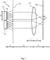
- Fig. 1 shows a principal sketch of a first laser printing system 100.
- the laser printing system 100 comprises two laser arrays 110 with semiconductor lasers 115 and an optical element 170.
- the semiconductor lasers 115 are VCSELs which are provided on a semiconductor chip. In this case all VCSELs 115 of one array 110 are provided on one chip.
- the optical element 170 is an imaging lens with a focal distance f.
- the arrays 110 have a width D perpendicular to the plane of the drawings which is diffusely imaged to a working plane 180 by means of the imaging lens.
- the width d of the diffuse image of each array 110 with the width D in the working plane 180 defines the width of a pixel in the working plane 180.
- the width of the pixels d is smaller than the width D of the respective array.
- the images of the arrays are thus demagnified.
- the distance b between the working plane 180 and the imaging lens or optical element 170 is bigger than the focal length f of the imaging lens.
- the optical element 170 or imaging lens defines together with the working plane 180 an object plane 150 in distance g bigger than the focal length of the imaging lens.
- the light emitting surfaces of the VCSELs 115 are not arranged in the object plane but behind the object plane in a distance such that no sharp projection of the light emitting surfaces of the VCSEL 115 is provided.
- the distance a between the light emitting layers of the VCSELs 115 and the object plane is chosen in a way that the laser light of at least two VCSEL 115 of one laser array 110 simultaneously illuminate an area element of a pixel.
- Figure 2 shows the arrangement of a divergence angle of laser light emitted by one VCSEL 115 in relation to the object plane 150 in more detail.
- the divergence angle of the VCSELs 115 is given by an angle ⁇ as shown in Figure 2 and defines the cone of laser light emitted by the single VCSEL 115.
- the VCSELs 115 in the laser array 110 do have a distance p with respect to each other (pitch).
- the relation between pitch p and distance a has to fulfill the condition: a • p * tan ⁇ ⁇ 1
- Laser light emitted by the VCSELs 115 of the laser array 110 overlap in the object plane 150 such that each area of the same size as the laser array 110 in the object plane 150 is illuminated by means of at least two VCSEL 115.
- Each area element of the pixel defined by the pixel size d is consequently also illuminated via the imaging lens by means of at least two VCSELs 115 of the respective laser array 110.
- the VCSELs of each laser array are driven in parallel and thus emit laser light at the same time.
- the image of the laser array 110 in the working plane 180 is diffuse in order to increase the homogeneity of the energy input to the object in the working plane 180 and improve the reliability with respect to malfunctions of single VCSEL.
- the total distance between the laser arrays 110 of the laser module and the working plane 180 may be increased by means of a micro-lens array 175 which may be combined with the laser array 110 as shown in Fig. 3 .
- the micro-lens array 175 may be arranged between the laser array 110 and the object plane 150 in order to decrease the divergence angle ⁇ of each VCSEL 115.
- the distance a and therefore the total distance to the working plane 150 has to be increased in order to fulfill the condition a • p*(tan ⁇ ) -1 if the pitch of the VCSELs 115 remains the same.
- an improvement of the condition discussed with respect to Fig. 2 may be achieved by taking into account an active diameter v of the VCSELs 115 in case of VCSELs 115 with circular aperture.
- the active diameter v corresponds to the diameter of the light emitting area of the active layer.
- the relation between active diameter v, pitch p and distance a has in this improved embodiment to fulfill the condition: a • p ⁇ v * 2 tan ⁇ ⁇ 1 .
- Fig. 4 shows a principal sketch of an arrangement of laser arrays 110 in a laser module of the laser printing system 100.
- the laser or VCSEL arrays 110 are not quadratic but rectangular, with the long side of the rectangle being arranged in the direction of the movement of the object (see Fig. 5 ). This allows higher total powers per pixel, without reducing the resolution in the lateral direction.
- the VCSEL arrays 110 are further arranged in two columns which are slightly shifted with respect to each other (cascaded or staggered arrangement). This enables a defined overlap with respect to the illumination of area elements of the object if the object moves perpendicular to the direction of the columns of VCSELs.
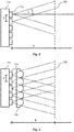
- Fig. 5 shows a principal sketch of a first arrangement of laser modules of the laser printing system 100.
- the laser modules comprise staggered or cascaded arrangements of laser arrays 110 as shown in Fig. 4 and an optical element 170.
- the optical element 170 images all laser arrays 110 of the respective laser modules to the working plane 180 of the laser printing system 100.
- the optical element 170 defines the total size Y of the laser module wherein the width of the arrangement of laser arrays 110 of the respective laser module defines the printing width y of one laser module.
- the laser modules are arranged in columns parallel to each other wherein each column is shifted such that a continuous area can be illuminated in the working plane 180 if the object moves in direction 250 relative to the laser modules.
- the printing area can thus be adapted to the size of the object in the working plane independent on the size Y and printing width y of the single laser module.
- the number of columns needed in order to continuously illuminate an object moving in the working plane 180 depends on the size Y and printing width y of the laser modules.
- the cascaded optical elements 170 may be fabricated as a single piece e.g. by glass molding. Alternatively, a lens array may be assembled from individual lenses by active or passive alignment.
- Fig. 6 shows a principal sketch of a second arrangement of laser modules of the laser printing system.
- the arrangement is quite similar to the arrangement discussed with respect to Fig. 5 .
- the laser arrays 110 of the laser modules are slanted (rotated around their center) with respect to a direction perpendicular to the direction of movement 250 of the object relative to the laser modules.
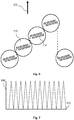
- This enables integrated intensity profiles with smooth slopes as shown in Figs. 7 and 8 , which may also overlap with the adjacent pixels, to improve the homogeneity of the total intensity distribution, especially if the pixels are slightly misaligned with respect to each other.
- Fig. 7 shows an integrated intensity profile in a direction 610 perpendicular to the direction of movement 250 of the object relative to the laser modules with every second pixel off in the arrangement of laser modules shown in Fig. 6 .
- the pixel profile is almost triangular, with large slopes that overlap with the adjacent pixels.
- Fig. 8 shows an integrated intensity profile with an arbitrary pattern of on/off switched pixel in the arrangement of laser modules shown in Fig. 6 .
- the numbers "1" and "0" indicate which of the adjacent laser arrays 110 are switched on or off.
- the integrated intensity profile shows the overlap of two or more neighboring pixels in the working plane 180.
- Fig. 9 shows a principal sketch of method steps of a method of laser printing. The shown sequence of steps does not necessarily imply the same sequence during execution of the method. Method steps may be executed in different order or in parallel.
- the object like a sheet of paper is moved in the working plane of the laser printing system relative to the laser module.
- laser light is emitted by means of the laser module comprising at least two laser arrays of semiconductor lasers and at least one optical element.
- the laser light emitted by the laser arrays is imaged, such that laser light of semiconductor lasers of one laser array is imaged to one pixel in the working plane and an area element of the pixel is illuminated by means of at least two semiconductor lasers.
- the object may be moved and at the same time laser light of the laser arrays may be emitted and imaged to the working plane.
- the maximum speed in the printing especially 3D printing process can be obtained when along a line all individual pixels can be written at the same time, i.e. by a separate laser or laser array per pixel.
- Typical line widths in a laser printing system or machine are in the order of 30 cm or more.
- the size or printing width of a laser module of individually addressable lasers or laser arrays is limited to a few cm. These laser modules correspond usually to one micro-channel cooler on which the laser modules are arranged.
- Said laser light sources 116 are so called overlap laser light sources 117 which are arranged such that the light of these overlap laser light sources 117 overlaps with light of laser light sources 116 of neighboring laser module.
- the pitch between neighboring laser modules is by at least the width of one laser light source 116 (e.g. 100 ⁇ m) smaller than the total printing width of the laser module.
- the maximum tolerance from the mechanical / optical alignment of neighboring laser modules is smaller than the width of one laser light source 116, it is sufficient to have - by design - an overlap of one laser light source 116 in order to avoid gaps in the working plane to which no laser light can be provided.
- the laser printing system may in this case be calibrated such that the overlap laser light sources 117 fill the unintended gap between the laser modules.
- the gaps and the width of one laser light source 116 it may be that one, two, three or even more of the overlap laser light sources 117 are used in order to enable a seamless illumination of the working plane.
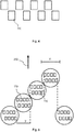
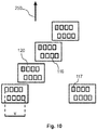
- Fig. 10 shows an embodiment of such an arrangement with overlap laser light sources 117 which are laser light source 116 which are arranged in an overlapping arrangement of neighboring laser modules which are laser sub-modules 120 in order to compensate potential misalignment of laser sub-modules 120 with respect to each other.
- the overlap laser light sources 117 are indicated by a line pattern.
- a laser light source 116 may comprise different as the previous embodiments only a single laser or in accordance with the previous embodiments a laser array such as laser arrays 110.
- the single lasers may comprise optical elements like micro-lenses. In case of laser arrays micro-lens arrays may be comprised.
- the arrangement of the laser sub-modules 120 is similar to the arrangement as shown in Fig. 5 .
- the laser modules shown in Fig. 5 are arranged such that each laser array 110 illuminates a dedicated pixel or area element in the working plane 180.
- the laser sub-modules 120 as shown in Fig. 10 are arranged such that in case of no alignment errors during assembly the overlap laser light sources 117 are adapted such that they can illuminate the same area element in the working plane 180 as a laser light source 116 of a neighboring laser sub-module 120.
- Fig. 11 shows an arrangement of laser modules similar to that of Fig. 5 with the difference that more than two columns and the demagnified image produced by the laser modules with the optical elements in the working plane 180 are shown.
- the arrangement of laser modules includes a plurality of laser modules 200 arranged in columns perpendicular to the direction of movement 250.
- the columns of the laser modules are staggered with respect to each other such that a first laser module 200 1 of a first column c1 of laser modules is adapted to illuminate a first area y1 in the working plane 180.
- the second module 200 2 of a second column c2 of laser modules is adapted to illuminate a second area y2 in the working plane 180, wherein the first area y1 is adjacent to the second area y2 such that continuous illumination of the object is enabled.
- the illuminated areas y1, y2 in the working plane 180 form a contiguous area in the direction perpendicular to the direction of movement.
- laser modules that are staggered in the direction of movement 250 form cascades.
- a first cascade k1 is formed by the first laser modules 200 1 , 200 2 , 200 n of the columns.
- a second cascade k2 is formed by the second laser modules 201 1 , 201 2 , 201 n of the columns and so on.
- the number of cascades is such that the sum of the individual printing widths y in a direction perpendicular to the direction of movement 250 covers the whole area to be illuminated in the working plane.
- the laser arrays 110 of the modules 200 are arranged as depicted in Fig. 4 .
- an optical element 175 associated with such an arrangement of the laser arrays 110 has a contour obtained from a circular or rotationally symmetrical contour, which is truncated onto opposing sides and wherein the opposing sides 1 of the optical element 175 are aligned with respect to each other along an axis which is preferably orientated in a direction perpendicular to the direction of movement 250. More precisely, in the case of the arrangement of the laser arrays as in Fig. 4 , the optical element 175 has the contour of a modified rectangle with two opposing circular segment-shaped short sides s that connect the parallel long sides 1.
- neighboring pixels at the border between one module 200 1 and a neighboring module 200 2 of one cascade k 1 and/or of one module 200 n of one cascade k1 and a neighboring module 201 1 of a neighboring cascade k2 can be illuminated with reduced time offset. This also increases the quality of the three-dimensional article.
- the arrangement of the VCSEL in laser array 110 defines the intensity profile. If the arrangement is substantially rectangular, i.e. the VCSELs are arranged in the array in rows and columns, the integrated intensity profile 600 of the array is substantially rectangular, i.e. the integrated intensity profile has a so-called "flat top" profile as depicted in Fig. 14 . In a module according to Fig. 4 , where several arrays 110 are switched on and several arrays are switched off, the integrated intensity of the module in a direction 610 perpendicular to the direction of movement 250 is as shown in Fig. 15 , i.e. has sharp edges.
- VCSELs in one array 110 are positioned in rows and columns and wherein the outer contour of the array is substantially polygonal, in particular, substantially hexagonal.
- the individual VCSELs are positioned at grid points that are staggered from one column to the next column, wherein the columns are oriented perpendicular to the direction of movement 250.
- the outer contour of the array has a hexagonal shape with two opposing parallel sides p which extend perpendicular to the direction of movement 250.
- the integrated intensity profile 600 of a laser array with a substantially hexagonal shape as shown in Fig. 13 has rounded edges and is similar to a Gaussian intensity distribution.
- the integrated intensity profile 600 along a direction 610 comprises rounded transitions as depicted in Fig. 17 . Hence, deviations from an average value of intensity are smaller.
- one pixel in the working area is illuminated by a multitude of semiconductor lasers of a laser array 110 at the same time.
- the total number of semiconductor lasers may be selected such that failure of less than a predetermined number of the semiconductor lasers reduces the output power of the laser array 110 only within a predetermined tolerance value. As a result thereof, the requirements with respect to the working life of the individual VCSELs may not be unusually high.
- the individual VCSELs of a laser array may be grouped in sub-groups with respect to their addressability by control signals.
- a sub-group may include at least two VCSELs.
- At least two sub-groups of VCSEL of one laser array may be individually addressable such that an output power of the laser array 110 is controllable by switching off one or more sub-groups of VCSEL.
- an embodiment may be provided where the semiconductor lasers of one laser array are individually addressable so that an output power of the laser array may be controlled by switching on/off individual semiconductor lasers.
- the semiconductor lasers or the laser arrays of the arrangement of laser modules can be further controlled such that a semiconductor laser or a laser array which is not used for illuminating can optionally be used for providing heat to the material in the working plane 180.
- a control device is provided which controls the semiconductor lasers or the laser arrays individually. This heating can be used in addition to the separate heating device described above or as an exclusive heating system that pre-heats the object to a working temperature.
- the arrangement of laser modules may include overlap light sources 117 as explained with reference to Fig. 10 .
- the overlap light sources 117 are preferably provided at the border between one module of one column to a neighboring module of a neighboring column, for example module 200 1 of column c1 and module 200 2 of column c2 in Fig. 13 and/or from one module in one cascade to a neighboring module in a neighboring cascade, for example module 200 n . in cascade k1 and module 201 1 in cascade k2 in Fig. 11 .
- the overlap light source 117 balances the energy loss resulting from a time offset of adjacent pixels perpendicular to the direction of movement 250 due to the staggered arrangement of a module and/or due to the cascaded arrangement of the modules.
- the overlap light sources 117 can be controlled in such a manner that energy losses due to time offset and/or energy losses or energy excesses due to misalignment of VCSELs or arrays can be compensated. Hence, the sum of energy that is provided to the working area by overlap light sources 117 can be adjusted to be the energy necessary for illuminating in the case of time offset zero and/or perfectly aligned VCSELs or arrays.
- the energy provided by the overlapping VCSELs or arrays can be selected depending on the type of building material. Influencing factors may be the heat conductivity of the object.
- the semiconductor lasers of the illumination unit are realized by VECSEL (Vertical External Cavity Surface Emitting Laser).
Landscapes
- Engineering & Computer Science (AREA)
- Materials Engineering (AREA)
- Chemical & Material Sciences (AREA)
- Physics & Mathematics (AREA)
- Optics & Photonics (AREA)
- Manufacturing & Machinery (AREA)
- Toxicology (AREA)
- Health & Medical Sciences (AREA)
- General Health & Medical Sciences (AREA)
- Mechanical Engineering (AREA)
- Plasma & Fusion (AREA)
- General Physics & Mathematics (AREA)
- Microelectronics & Electronic Packaging (AREA)
- Electromagnetism (AREA)
- Condensed Matter Physics & Semiconductors (AREA)
- Semiconductor Lasers (AREA)
- Laser Beam Processing (AREA)
- Manufacture Or Reproduction Of Printing Formes (AREA)
- Printers Or Recording Devices Using Electromagnetic And Radiation Means (AREA)
- Powder Metallurgy (AREA)
Priority Applications (1)
| Application Number | Priority Date | Filing Date | Title |
|---|---|---|---|
| EP14812255.9A EP3083254B1 (en) | 2013-12-17 | 2014-12-16 | Laser printing system |
Applications Claiming Priority (3)
| Application Number | Priority Date | Filing Date | Title |
|---|---|---|---|
| EP13197751 | 2013-12-17 | ||
| EP14812255.9A EP3083254B1 (en) | 2013-12-17 | 2014-12-16 | Laser printing system |
| PCT/EP2014/077931 WO2015091459A1 (en) | 2013-12-17 | 2014-12-16 | Laser printing system |
Publications (2)
| Publication Number | Publication Date |
|---|---|
| EP3083254A1 EP3083254A1 (en) | 2016-10-26 |
| EP3083254B1 true EP3083254B1 (en) | 2019-06-26 |
Family
ID=49886642
Family Applications (3)
| Application Number | Title | Priority Date | Filing Date |
|---|---|---|---|
| EP14812255.9A Active EP3083254B1 (en) | 2013-12-17 | 2014-12-16 | Laser printing system |
| EP20165035.5A Ceased EP3705300A1 (en) | 2013-12-17 | 2014-12-16 | Laser printing system |
| EP14824420.5A Active EP3079912B1 (en) | 2013-12-17 | 2014-12-16 | Laser printing system |
Family Applications After (2)
| Application Number | Title | Priority Date | Filing Date |
|---|---|---|---|
| EP20165035.5A Ceased EP3705300A1 (en) | 2013-12-17 | 2014-12-16 | Laser printing system |
| EP14824420.5A Active EP3079912B1 (en) | 2013-12-17 | 2014-12-16 | Laser printing system |
Country Status (10)
| Country | Link |
|---|---|
| US (5) | US10723139B2 (cg-RX-API-DMAC7.html) |
| EP (3) | EP3083254B1 (cg-RX-API-DMAC7.html) |
| JP (3) | JP6310560B2 (cg-RX-API-DMAC7.html) |
| KR (1) | KR102283851B1 (cg-RX-API-DMAC7.html) |
| CN (3) | CN105829113B (cg-RX-API-DMAC7.html) |
| BR (1) | BR112016013879A2 (cg-RX-API-DMAC7.html) |
| ES (1) | ES2799123T3 (cg-RX-API-DMAC7.html) |
| MX (1) | MX2016007805A (cg-RX-API-DMAC7.html) |
| RU (2) | RU2674511C1 (cg-RX-API-DMAC7.html) |
| WO (2) | WO2015091485A1 (cg-RX-API-DMAC7.html) |
Families Citing this family (145)
| Publication number | Priority date | Publication date | Assignee | Title |
|---|---|---|---|---|
| GB0816308D0 (en) | 2008-09-05 | 2008-10-15 | Mtt Technologies Ltd | Optical module |
| CN105829113B (zh) * | 2013-12-17 | 2018-05-15 | Eos有限公司电镀光纤系统 | 激光打印系统 |
| US10029421B2 (en) * | 2014-09-18 | 2018-07-24 | 3Dm Digital Manufacturing Ltd | Device and a method for 3D printing and manufacturing of materials using quantum cascade lasers |
| DE102015200134A1 (de) * | 2015-01-08 | 2016-07-14 | Trumpf Laser- Und Systemtechnik Gmbh | Modular aufgebaute SLM- oder SLS-Bearbeitungsmaschine |
| US20180056585A1 (en) * | 2015-05-12 | 2018-03-01 | Gizmo 3D Printers | Improvements in 3d printing |
| WO2016189510A1 (en) * | 2015-05-27 | 2016-12-01 | Landa Labs (2012) Ltd. | Imaging device |
| JP6505517B2 (ja) * | 2015-06-18 | 2019-04-24 | ローランドディー.ジー.株式会社 | 三次元造形装置 |
| EP3325276B1 (en) * | 2015-07-23 | 2018-12-12 | Koninklijke Philips N.V. | Laser printing system |
| DE102015115810A1 (de) | 2015-09-18 | 2017-03-23 | Osram Opto Semiconductors Gmbh | Optoelektronisches Halbleiterbauteil und 3D-Drucker |
| DE102015219866A1 (de) * | 2015-10-13 | 2017-04-13 | Eos Gmbh Electro Optical Systems | Vorrichtung und Verfahren zum Herstellen eines dreidimensionalen Objekts |
| US11691341B2 (en) | 2015-10-30 | 2023-07-04 | Seurat Technologies, Inc. | Part manipulation using printed manipulation points |
| DE102015221623A1 (de) * | 2015-11-04 | 2017-05-04 | Eos Gmbh Electro Optical Systems | Belichteroptik und Vorrichtung zum Herstellen eines dreidimensionalen Objekts |
| ES2940909T3 (es) * | 2015-11-16 | 2023-05-12 | Renishaw Plc | Módulo para aparato de fabricación aditiva |
| US10471543B2 (en) | 2015-12-15 | 2019-11-12 | Lawrence Livermore National Security, Llc | Laser-assisted additive manufacturing |
| CN108495741B (zh) * | 2016-01-20 | 2020-08-04 | 惠普发展公司,有限责任合伙企业 | 打印设备 |
| EP3411170A4 (en) | 2016-01-28 | 2020-02-12 | Seurat Technologies, Inc. | SYSTEM AND METHOD FOR ADDITIVE MANUFACTURING AND SPATIAL HEAT TREATMENT |
| US11148319B2 (en) | 2016-01-29 | 2021-10-19 | Seurat Technologies, Inc. | Additive manufacturing, bond modifying system and method |
| JP6959698B2 (ja) * | 2016-04-25 | 2021-11-05 | レニショウ パブリック リミテッド カンパニーRenishaw Public Limited Company | アディティブ製造装置内の複数のスキャナの較正方法 |
| EP3458251A4 (en) * | 2016-05-17 | 2020-01-08 | Hewlett-Packard Development Company, L.P. | 3D PRINTER WITH ADJUSTED FUSION RADIATION EMISSION |
| US10717230B2 (en) * | 2016-06-16 | 2020-07-21 | Xerox Corporation | Line laser imager for thermoplastic selective laser sintering |
| KR101787718B1 (ko) * | 2016-06-21 | 2017-11-16 | 한국기계연구원 | 3차원 레이저 프린팅 장치 및 방법 |
| CN109789634B (zh) * | 2016-07-20 | 2021-09-07 | 芯特技术股份有限公司 | 保护元件 |
| CN106216862B (zh) * | 2016-07-20 | 2018-10-16 | 华中科技大学 | 一种基于电弧增材和高能束流减材的复合制造方法及装置 |
| US10821717B2 (en) | 2016-07-22 | 2020-11-03 | General Electric Company | Layer orientation control for pixel-based additive manufacturing |
| US10953470B2 (en) | 2016-08-31 | 2021-03-23 | Raytheon Technologies Corporation | Scanning mirror navigation apparatus and method |
| CN106229808B (zh) * | 2016-09-20 | 2023-08-29 | 中国电子科技集团公司第十三研究所 | 脉冲激光器 |
| DE102016218887A1 (de) * | 2016-09-29 | 2018-03-29 | SLM Solutions Group AG | Herstellen dreidimensionaler Werkstücke mittels einer Mehrzahl von Bestrahlungseinheiten |
| WO2018064349A1 (en) | 2016-09-30 | 2018-04-05 | Velo3D, Inc. | Three-dimensional objects and their formation |
| JP2018059757A (ja) * | 2016-10-04 | 2018-04-12 | オムロンオートモーティブエレクトロニクス株式会社 | 投光光学系、物体検出装置 |
| DE102016120044A1 (de) * | 2016-10-20 | 2018-04-26 | Cl Schutzrechtsverwaltungs Gmbh | Vorrichtung zur additiven Herstellung dreidimensionaler Objekte |
| FR3057794B1 (fr) * | 2016-10-26 | 2019-07-19 | Addup | Perfectionnements a la fabrication additive selective |
| FR3057793B1 (fr) * | 2016-10-26 | 2021-04-09 | Fives Michelin Additive Solutions | Appareil et procede pour fabriquer un objet tridimensionnel |
| US10919285B2 (en) * | 2016-11-07 | 2021-02-16 | General Electric Company | Method and system for x-ray backscatter inspection of additive manufactured parts |
| DE102016222187A1 (de) * | 2016-11-11 | 2018-05-17 | Trumpf Laser- Und Systemtechnik Gmbh | Verfahren zum Bestimmen eines Strahlprofils eines Laserstrahls und Bearbeitungsmaschine |
| DE102016123000B3 (de) * | 2016-11-29 | 2017-12-14 | Scansonic Mi Gmbh | Verfahren zur Überwachung eines Schutzglases und Überwachungsvorrichtung |
| US10399179B2 (en) | 2016-12-14 | 2019-09-03 | General Electric Company | Additive manufacturing systems and methods |
| US10589508B2 (en) * | 2016-12-15 | 2020-03-17 | General Electric Company | Additive manufacturing systems and methods |
| US10583530B2 (en) * | 2017-01-09 | 2020-03-10 | General Electric Company | System and methods for fabricating a component with laser array |
| US10549519B2 (en) * | 2017-01-12 | 2020-02-04 | Caterpillar Inc. | Systems and methods for calibrating additive manufacturing operations based on energy density |
| GB201701355D0 (en) | 2017-01-27 | 2017-03-15 | Renishaw Plc | Direct laser writing and chemical etching |
| US11548094B2 (en) * | 2017-02-15 | 2023-01-10 | General Electric Company | System and methods for fabricating a component with laser array |
| US10317881B2 (en) | 2017-03-01 | 2019-06-11 | General Electric Company | Parallelized CAD using multi laser additive printing |
| US10695865B2 (en) * | 2017-03-03 | 2020-06-30 | General Electric Company | Systems and methods for fabricating a component with at least one laser device |
| JP6844347B2 (ja) * | 2017-03-15 | 2021-03-17 | 株式会社リコー | レーザ処理装置 |
| EP3382828A1 (en) * | 2017-03-31 | 2018-10-03 | Koninklijke Philips N.V. | Inherently safe laser arrangement comprising a vertical cavity surface emitting laser |
| US10906132B2 (en) | 2017-03-31 | 2021-02-02 | General Electric Company | Scan strategies for efficient utilization of laser arrays in direct metal laser melting (DMLM) |
| CN115464159B (zh) | 2017-05-11 | 2024-07-16 | 速尔特技术有限公司 | 用于增材制造的图案化光的开关站射束路由 |
| EP3621809A4 (en) | 2017-05-11 | 2021-01-20 | Seurat Technologies, Inc. | SOLID-STATE ROUTING OF STRUCTURED LIGHT TO OPTIMIZE GENERATIVE MANUFACTURING |
| US10882248B2 (en) * | 2017-06-28 | 2021-01-05 | 3D Systems, Inc. | Three dimensional printer for fusing powders with surface coloration using a VCSEL array |
| DE102017210994A1 (de) | 2017-06-28 | 2019-01-03 | Eos Gmbh Electro Optical Systems | Messsystem für eine Vorrichtung zum generativen Herstellen eines dreidimensionalen Objekts |
| US11407034B2 (en) | 2017-07-06 | 2022-08-09 | OmniTek Technology Ltda. | Selective laser melting system and method of using same |
| US20210206057A1 (en) * | 2017-07-28 | 2021-07-08 | Hewlett-Packard Development Company, L.P. | Three-dimensional printer with movement device |
| GB201712726D0 (en) * | 2017-08-08 | 2017-09-20 | Landa Labs (2012) Ltd | Electric current and heat mitigation in a printing machine writing module |
| US10766242B2 (en) * | 2017-08-24 | 2020-09-08 | General Electric Company | System and methods for fabricating a component using a consolidating device |
| CN107457986A (zh) * | 2017-08-26 | 2017-12-12 | 吴江中瑞机电科技有限公司 | 超高速循环式光固化3d打印机 |
| EP3451470A1 (en) | 2017-08-30 | 2019-03-06 | Koninklijke Philips N.V. | Laser arrangement comprising a vcsel array |
| JP6642546B2 (ja) * | 2017-09-21 | 2020-02-05 | 日亜化学工業株式会社 | 波長ビーム結合装置 |
| TWI719261B (zh) | 2017-09-29 | 2021-02-21 | 國立中興大學 | 利用光學讀寫頭之積層製造裝置 |
| US11084132B2 (en) | 2017-10-26 | 2021-08-10 | General Electric Company | Diode laser fiber array for contour of powder bed fabrication or repair |
| WO2019099928A2 (en) * | 2017-11-17 | 2019-05-23 | Kevin Friesth | Advanced automated fabrication system and methods for thermal and mechanical components utilizing quadratic or squared hybrid direct laser sintering, direct metal laser sintering, cnc, thermal spraying, direct metal deposition and frictional stir welding |
| US11027336B2 (en) * | 2017-11-21 | 2021-06-08 | Hamilton Sundstrand Corporation | Splatter shield systems and methods for additive manufacturing |
| CN109940879B (zh) * | 2017-12-20 | 2023-08-29 | 广州中国科学院先进技术研究所 | 一种新型可见光固化3d打印机的控制系统及方法 |
| EP3509170A1 (en) | 2018-01-05 | 2019-07-10 | Koninklijke Philips N.V. | Energy efficient laser arrangement |
| WO2019143314A1 (en) | 2018-01-16 | 2019-07-25 | Hewlett-Packard Development Company, L.P. | Three dimensional printing system |
| EP3518356A1 (en) * | 2018-01-24 | 2019-07-31 | Koninklijke Philips N.V. | Laser arrangement with irregular emission pattern |
| EP3524409A1 (en) * | 2018-02-09 | 2019-08-14 | CL Schutzrechtsverwaltungs GmbH | Apparatus for additively manufacturing three-dimensional objects |
| KR102288791B1 (ko) * | 2018-03-23 | 2021-08-10 | 프리메탈스 테크놀로지스 재팬 가부시키가이샤 | 레이저 가공 헤드 및 레이저 가공 장치 그리고 레이저 가공 헤드의 조정 방법 |
| US10875094B2 (en) * | 2018-03-29 | 2020-12-29 | Vulcanforms Inc. | Additive manufacturing systems and methods |
| EP3552806A1 (en) | 2018-04-09 | 2019-10-16 | Nederlandse Organisatie voor toegepast- natuurwetenschappelijk onderzoek TNO | Method of apparatus for forming an object by means of additive manufacturing |
| CN108581215B (zh) * | 2018-05-14 | 2020-01-31 | 苏州米氪激光技术服务有限公司 | 一种双花纹地毯加工用的交错式激光雕刻设备 |
| GB201807830D0 (en) * | 2018-05-15 | 2018-06-27 | Renishaw Plc | Laser beam scanner |
| WO2019236106A1 (en) * | 2018-06-08 | 2019-12-12 | Hewlett-Packard Development Company, L.P. | Printing devices |
| EP3588702A1 (en) * | 2018-06-26 | 2020-01-01 | Koninklijke Philips N.V. | Vcsel array with small pulse delay |
| WO2020014344A1 (en) | 2018-07-10 | 2020-01-16 | 3D Systems, Inc. | Three dimensional (3d) printer with high resolution light engine |
| US11325299B2 (en) | 2018-07-16 | 2022-05-10 | Massachusetts Institute Of Technology | Additive manufacturing via optical aperture division multiplexing |
| EP3598591A1 (en) * | 2018-07-17 | 2020-01-22 | Koninklijke Philips N.V. | Laser arrangement with reduced building height |
| DE102018211972B4 (de) * | 2018-07-18 | 2020-04-23 | Trumpf Laser Gmbh | Optische Anordnung zur variablen Erzeugung eines Multifoki-Profils, sowie Verfahren zum Betrieb und Verwendung einer solchen Anordnung |
| US11426818B2 (en) | 2018-08-10 | 2022-08-30 | The Research Foundation for the State University | Additive manufacturing processes and additively manufactured products |
| KR20210074339A (ko) | 2018-10-10 | 2021-06-21 | 스탬 베그 코포레이션 | 연속 유동 미세생물반응기 |
| US11872757B2 (en) * | 2018-10-30 | 2024-01-16 | Hewlett-Packard Development Company, L.P. | Microwave energy emitters with tips |
| KR102736296B1 (ko) | 2018-11-08 | 2024-11-29 | 삼성전자주식회사 | 홀로그래픽 디스플레이 장치 |
| DE102018219302A1 (de) | 2018-11-12 | 2020-05-14 | Eos Gmbh Electro Optical Systems | Selektives Sintern von polymerbasiertem Aufbaumaterial |
| DE102018219303A1 (de) | 2018-11-12 | 2020-05-14 | Eos Gmbh Electro Optical Systems | Verzugsoptimiertes Kunststoffpulver |
| KR102130343B1 (ko) * | 2018-11-14 | 2020-08-06 | 한국기계연구원 | 레이저와 분말을 이용한 3차원 형상 제조장치 |
| WO2020121959A1 (ja) * | 2018-12-14 | 2020-06-18 | 株式会社デンソー | 光学的測距装置、レーザ発光装置およびその製造方法 |
| US12011873B2 (en) | 2018-12-14 | 2024-06-18 | Seurat Technologies, Inc. | Additive manufacturing system for object creation from powder using a high flux laser for two-dimensional printing |
| JP7172963B2 (ja) * | 2018-12-14 | 2022-11-16 | 株式会社デンソー | 光学的測距装置、レーザ発光装置の製造方法 |
| CA3124097A1 (en) | 2018-12-19 | 2020-06-25 | Seurat Technologies, Inc. | Additive manufacturing system using a pulse modulated laser for two-dimensional printing |
| KR102171814B1 (ko) * | 2018-12-28 | 2020-10-29 | 한국광기술원 | 분할 성형 지원형 광경화 3d 프린터 |
| CN118003625A (zh) * | 2019-01-24 | 2024-05-10 | 沃尔特·沃伊特 | 用于超高吞吐量增材制造的系统、方法及材料 |
| CN111654680B (zh) * | 2019-03-04 | 2024-08-13 | 北京谦恒德科技有限公司 | 一种数字光处理光机的投影拼接方法及装置 |
| DE102019204032B4 (de) * | 2019-03-25 | 2021-09-30 | Fraunhofer-Gesellschaft zur Förderung der angewandten Forschung e.V. | Vorrichtung zur Erzeugung einer räumlich modulierbaren Leistungsdichteverteilung aus Laserstrahlung |
| CN110142406B (zh) * | 2019-03-29 | 2020-05-19 | 西北大学 | 二维光纤面阵高精度激光3d金属打印机及其打印控制方法 |
| CN109986079B (zh) * | 2019-03-29 | 2020-04-14 | 西北大学 | 激光线阵3d金属打印机及其文件转换、打印控制方法 |
| EP3722075B1 (en) * | 2019-04-08 | 2022-06-29 | LayerWise N.V. | Three-dimensional printing system optimizing seams between zones for multiple energy beams |
| EP3748287B1 (en) * | 2019-06-06 | 2021-10-13 | TRUMPF Photonic Components GmbH | Vcsel based pattern projector |
| US11230058B2 (en) | 2019-06-07 | 2022-01-25 | The Boeing Company | Additive manufacturing using light source arrays to provide multiple light beams to a build medium via a rotatable reflector |
| CN114174045B (zh) * | 2019-07-08 | 2024-05-28 | 尼康Slm方案股份公司 | 光学单元和用于制造三维工件的系统 |
| CA3148849A1 (en) | 2019-07-26 | 2021-02-04 | Velo3D, Inc. | Quality assurance in formation of three-dimensional objects |
| CN110899986B (zh) * | 2019-08-16 | 2022-02-01 | 广东省广袤科技有限公司 | 激光扫描刻蚀制造二维码方法及其装置 |
| CN110524874B (zh) * | 2019-08-23 | 2022-03-08 | 源秩科技(上海)有限公司 | 光固化3d打印装置及其打印方法 |
| CN110412544A (zh) * | 2019-08-23 | 2019-11-05 | 上海禾赛光电科技有限公司 | 激光发射系统以及包括所述激光发射系统的激光雷达 |
| KR102367742B1 (ko) * | 2019-12-10 | 2022-02-25 | (주)캐리마 | 선형광원 장치 및 이를 포함하는 3d프린터 |
| WO2021145825A1 (en) * | 2020-01-17 | 2021-07-22 | Ams Sensors Singapore Pte. Ltd. | Linear optical device |
| UY39063A (es) * | 2020-02-03 | 2021-08-31 | Stamm Vegh Corp | Plataforma, sistemas y dispositivos para impresiones 3d |
| JP7463782B2 (ja) * | 2020-03-17 | 2024-04-09 | 富士フイルムビジネスイノベーション株式会社 | 発光素子アレイ、発光装置、光学装置、計測装置及び情報処理装置 |
| US11862942B2 (en) * | 2020-06-19 | 2024-01-02 | Lumentum Operations Llc | Vertical-cavity surface-emitting laser array with a tilted emitter pattern |
| CN111605191A (zh) * | 2020-06-24 | 2020-09-01 | 深圳市智能派科技有限公司 | 一种多尺寸光固化3d打印机拼接光源 |
| US20220062998A1 (en) * | 2020-08-27 | 2022-03-03 | Apple Inc. | Novel architectures for high-throughput additive manufacturing |
| US11707883B2 (en) | 2020-11-20 | 2023-07-25 | General Electric Company | Foil interaction device for additive manufacturing |
| US12162074B2 (en) | 2020-11-25 | 2024-12-10 | Lawrence Livermore National Security, Llc | System and method for large-area pulsed laser melting of metallic powder in a laser powder bed fusion application |
| US11865780B2 (en) | 2021-02-26 | 2024-01-09 | General Electric Company | Accumalator assembly for additive manufacturing |
| CN113001988B (zh) * | 2021-03-12 | 2021-11-12 | 江苏乾度智造高科技有限公司 | 三维打印装置及方法 |
| IT202100008102A1 (it) | 2021-04-01 | 2021-07-01 | 3D New Tech S R L | Sistema multi laser per additive manufacturing |
| US12502839B2 (en) | 2021-05-12 | 2025-12-23 | Peridot Print Llc | Print agent coverage amounts |
| IT202100013136A1 (it) | 2021-05-21 | 2021-08-21 | 3D New Tech S R L | Sistema multi laser per additive manufacturing |
| US11951679B2 (en) | 2021-06-16 | 2024-04-09 | General Electric Company | Additive manufacturing system |
| US11599084B2 (en) * | 2021-06-18 | 2023-03-07 | Kyndryl, Inc. | Early notification system of degradation of 3D printed parts |
| US11731367B2 (en) | 2021-06-23 | 2023-08-22 | General Electric Company | Drive system for additive manufacturing |
| US11958249B2 (en) | 2021-06-24 | 2024-04-16 | General Electric Company | Reclamation system for additive manufacturing |
| US11958250B2 (en) | 2021-06-24 | 2024-04-16 | General Electric Company | Reclamation system for additive manufacturing |
| US11826950B2 (en) | 2021-07-09 | 2023-11-28 | General Electric Company | Resin management system for additive manufacturing |
| US20240320403A1 (en) * | 2021-07-14 | 2024-09-26 | Hewlett-Packard Development Company, L.P. | Lattice cell modifications |
| DE102021208911A1 (de) | 2021-08-13 | 2023-02-16 | Eos Gmbh Electro Optical Systems | Verbesserung der Positionsgenauigkeit der Energiezufuhr in einer additiven Fertigungsvorrichtung |
| US12370741B2 (en) | 2021-08-13 | 2025-07-29 | General Electric Company | Material deposition assembly for additive manufacturing |
| US11827037B2 (en) * | 2021-08-23 | 2023-11-28 | Xerox Corporation | Semiconductor array imager for printing systems |
| US20230054034A1 (en) * | 2021-08-23 | 2023-02-23 | Palo Alto Research Center Incorporated | 3d package for semiconductor thermal management |
| US20230056905A1 (en) * | 2021-08-23 | 2023-02-23 | Palo Alto Research Center Incorporated | Independently-addressable high power surface-emitting laser array with tight-pitch packing |
| US12296535B2 (en) | 2021-08-24 | 2025-05-13 | General Electric Company | Attachment structure for additive manufacturing |
| US11813799B2 (en) | 2021-09-01 | 2023-11-14 | General Electric Company | Control systems and methods for additive manufacturing |
| WO2023059618A1 (en) | 2021-10-07 | 2023-04-13 | Additive Monitoring Systems, Llc | Structured light part quality monitoring for additive manufacturing and methods of use |
| US20240418236A1 (en) * | 2021-10-29 | 2024-12-19 | Hewlett-Packard Development Company, L.P. | Flexible structures |
| US11987008B2 (en) | 2022-01-11 | 2024-05-21 | General Electric Company | Irradiation sequences for consolidating powder material in an additive manufacturing machine |
| EP4249216A1 (en) | 2022-03-23 | 2023-09-27 | General Electric Company | Systems and methods for additive manufacturing |
| JP2023141779A (ja) * | 2022-03-24 | 2023-10-05 | セイコーエプソン株式会社 | 加工ヘッドおよびレーザー加工装置 |
| CN114536772B (zh) * | 2022-04-21 | 2022-07-12 | 南京铖联激光科技有限公司 | 3d打印系统中智能分区控制系统及其控制方法 |
| KR20240025737A (ko) * | 2022-08-19 | 2024-02-27 | 한국전자기술연구원 | 열 쏠림 현상 최소화를 위한 공구 경로 패턴 면적에 따른 공구 경로 생성 방법 |
| US12403654B2 (en) | 2022-09-30 | 2025-09-02 | General Electric Company | Systems and methods for additive manufacturing |
| CN116277938A (zh) * | 2023-02-09 | 2023-06-23 | 京东方科技集团股份有限公司 | 一种光固化3d打印机及打印方法 |
| CN116352255A (zh) * | 2023-03-13 | 2023-06-30 | 东莞市中麒光电技术有限公司 | 多激光组合的焊接方法和装置 |
| CN116277983A (zh) * | 2023-04-07 | 2023-06-23 | 南京铖联激光科技有限公司 | 一种slm打印机的多激光控制方法 |
| US20240408674A1 (en) * | 2023-06-09 | 2024-12-12 | General Electric Company | Systems and methods for additively manufacturing three-dimensional objects with array of laser diodes |
| CN117021569B (zh) * | 2023-08-24 | 2024-07-16 | 爱司凯科技股份有限公司 | 基于图像数据分割平移的面阵激光连续移动3d打印方法 |
| CN117428210B (zh) * | 2023-12-20 | 2024-03-08 | 中国商用飞机有限责任公司 | 多激光选区熔融搭接方法 |
| DE102024200430A1 (de) * | 2024-01-17 | 2025-07-17 | Eos Gmbh Electro Optical Systems | Schutzvorrichtung für einen Belichter einer additiven Herstellvorrichtung |
Family Cites Families (29)
| Publication number | Priority date | Publication date | Assignee | Title |
|---|---|---|---|---|
| US5745153A (en) * | 1992-12-07 | 1998-04-28 | Eastman Kodak Company | Optical means for using diode laser arrays in laser multibeam printers and recorders |
| US5940113A (en) | 1994-12-19 | 1999-08-17 | Xerox Corporation | Lensless printing system with a light bar printhead |
| EP0781661A1 (en) * | 1995-12-22 | 1997-07-02 | Xerox Corporation | Increased pixel density and increased printing speed in a xerographic line printer with multiple linear arrays of surface emitting lasers |
| CN1299167A (zh) * | 1999-08-30 | 2001-06-13 | 贝尔-福斯公司 | 通过电阻元件提供插头放电的插座 |
| US6393038B1 (en) * | 1999-10-04 | 2002-05-21 | Sandia Corporation | Frequency-doubled vertical-external-cavity surface-emitting laser |
| US6264981B1 (en) * | 1999-10-27 | 2001-07-24 | Anesta Corporation | Oral transmucosal drug dosage using solid solution |
| US6353502B1 (en) | 2000-06-13 | 2002-03-05 | Eastman Kodak Company | VCSEL field correction |
| JP2002019177A (ja) * | 2000-07-06 | 2002-01-23 | Seiko Epson Corp | 光プリンタヘッド |
| JP2002316363A (ja) * | 2001-02-16 | 2002-10-29 | Fuji Photo Film Co Ltd | 光造形装置及び露光ユニット |
| DE10111871A1 (de) | 2001-03-13 | 2002-09-19 | Heidelberger Druckmasch Ag | Bebilderungseinrichtung für eine Druckform mit einem Array von VCSEL-Lichtquellen |
| CN100463484C (zh) * | 2001-03-29 | 2009-02-18 | 松下电器产业株式会社 | 图像写入装置,光源,光源单元,微透镜以及微透镜的制造方法 |
| JP2003080604A (ja) * | 2001-09-10 | 2003-03-19 | Fuji Photo Film Co Ltd | 積層造形装置 |
| US6894712B2 (en) * | 2002-04-10 | 2005-05-17 | Fuji Photo Film Co., Ltd. | Exposure head, exposure apparatus, and application thereof |
| DE10235434A1 (de) * | 2002-08-02 | 2004-02-12 | Eos Gmbh Electro Optical Systems | Vorrichtung und Verfahren zum Herstellen eins dreidimensionalen Objekts mittels eines generativen Fertigungsverfahrens |
| DE10308708A1 (de) * | 2003-02-28 | 2004-09-09 | Hentze-Lissotschenko Patentverwaltungs Gmbh & Co.Kg | Vorrichtung zur Beaufschlagung eines Objektes mit Laserstrahlung, Bearbeitungsvorrichtung für die Bearbeitung eines Objektes sowie Druckvorrichtung für das Drucken von Bildinformationen |
| US7059530B2 (en) * | 2003-04-24 | 2006-06-13 | Psion Teklogix,Inc. | Heated protective window for an optical scanning device |
| JP2007508596A (ja) | 2003-10-17 | 2007-04-05 | エクスプレイ リミテッド | 投影システムに使用する光学システムおよび方法 |
| US20050151828A1 (en) | 2004-01-14 | 2005-07-14 | Xerox Corporation. | Xerographic printing system with VCSEL-micro-optic laser printbar |
| US7995084B2 (en) * | 2007-01-25 | 2011-08-09 | Seiko Epson Corporation | Line head and an image forming apparatus using the line head |
| JP4238938B2 (ja) * | 2007-05-30 | 2009-03-18 | パナソニック電工株式会社 | 積層造形装置 |
| JP2009056796A (ja) * | 2007-08-07 | 2009-03-19 | Seiko Epson Corp | 露光ヘッド及びそれを用いた画像形成装置 |
| JP2009158709A (ja) * | 2007-12-26 | 2009-07-16 | Seiko Epson Corp | 面発光型半導体レーザアレイおよび面発光型半導体レーザ |
| JP4548497B2 (ja) | 2008-03-04 | 2010-09-22 | カシオ計算機株式会社 | 有機elヘッドおよびそれを用いた印刷装置 |
| US8253780B2 (en) | 2008-03-04 | 2012-08-28 | Genie Lens Technology, LLC | 3D display system using a lenticular lens array variably spaced apart from a display screen |
| JP5894529B2 (ja) * | 2009-08-20 | 2016-03-30 | コーニンクレッカ フィリップス エヌ ヴェKoninklijke Philips N.V. | 設定変更可能な輝度分布を備えるレーザー装置 |
| CN102905905B (zh) | 2010-03-18 | 2016-03-09 | 皇家飞利浦电子股份有限公司 | 激光烧结设备和用于控制激光烧结设备的方法 |
| JP2012153029A (ja) * | 2011-01-26 | 2012-08-16 | Fuji Xerox Co Ltd | 露光装置及び画像形成装置 |
| CN105829113B (zh) * | 2013-12-17 | 2018-05-15 | Eos有限公司电镀光纤系统 | 激光打印系统 |
| JP7149834B2 (ja) | 2018-12-17 | 2022-10-07 | キヤノン株式会社 | シンチレータの製造方法 |
-
2014
- 2014-12-16 CN CN201480068452.1A patent/CN105829113B/zh active Active
- 2014-12-16 JP JP2016538064A patent/JP6310560B2/ja active Active
- 2014-12-16 CN CN201480075736.3A patent/CN105980159B/zh active Active
- 2014-12-16 EP EP14812255.9A patent/EP3083254B1/en active Active
- 2014-12-16 BR BR112016013879A patent/BR112016013879A2/pt not_active Application Discontinuation
- 2014-12-16 KR KR1020167015838A patent/KR102283851B1/ko active Active
- 2014-12-16 JP JP2016539227A patent/JP6585597B2/ja active Active
- 2014-12-16 MX MX2016007805A patent/MX2016007805A/es unknown
- 2014-12-16 WO PCT/EP2014/077967 patent/WO2015091485A1/en not_active Ceased
- 2014-12-16 US US15/034,963 patent/US10723139B2/en active Active
- 2014-12-16 CN CN201810337981.7A patent/CN108582769B/zh active Active
- 2014-12-16 EP EP20165035.5A patent/EP3705300A1/en not_active Ceased
- 2014-12-16 RU RU2016123826A patent/RU2674511C1/ru active
- 2014-12-16 RU RU2016128798A patent/RU2656205C1/ru not_active IP Right Cessation
- 2014-12-16 EP EP14824420.5A patent/EP3079912B1/en active Active
- 2014-12-16 WO PCT/EP2014/077931 patent/WO2015091459A1/en not_active Ceased
- 2014-12-16 ES ES14824420T patent/ES2799123T3/es active Active
- 2014-12-16 US US15/103,888 patent/US10518555B2/en active Active
-
2019
- 2019-06-27 JP JP2019119534A patent/JP6810199B2/ja active Active
-
2020
- 2020-06-16 US US16/902,675 patent/US11260583B2/en active Active
-
2022
- 2022-01-21 US US17/581,046 patent/US11858204B2/en active Active
-
2023
- 2023-11-20 US US18/514,899 patent/US12172372B2/en active Active
Non-Patent Citations (1)
| Title |
|---|
| None * |
Also Published As
Similar Documents
| Publication | Publication Date | Title |
|---|---|---|
| EP3083254B1 (en) | Laser printing system | |
| JP2017501052A5 (cg-RX-API-DMAC7.html) | ||
| JP5944330B2 (ja) | 印刷装置及び印刷装置を制御する方法 | |
| JP2013527809A5 (cg-RX-API-DMAC7.html) | ||
| EP2009482B1 (en) | Multi-beam optical scanning device and image forming apparatus using the same | |
| US20050151828A1 (en) | Xerographic printing system with VCSEL-micro-optic laser printbar | |
| EP2865056B1 (en) | Laser module for homogeneous line-shaped intensity profiles | |
| JP4952028B2 (ja) | マイクロレンズ付き発光素子アレイチップ及び光書き込みヘッド | |
| US20220258424A1 (en) | Additive manufacturing machines for the additive manufacturing of an object layer-by-layer | |
| HK1050571A1 (en) | Image-making device with vcsel light resource array for machine plate | |
| HK1050571B (en) | Image-making device with vcsel light resource array for machine plate | |
| HK1092423A (en) | Method for image generation on a recording material |
Legal Events
| Date | Code | Title | Description |
|---|---|---|---|
| PUAI | Public reference made under article 153(3) epc to a published international application that has entered the european phase |
Free format text: ORIGINAL CODE: 0009012 |
|
| 17P | Request for examination filed |
Effective date: 20160718 |
|
| AK | Designated contracting states |
Kind code of ref document: A1 Designated state(s): AL AT BE BG CH CY CZ DE DK EE ES FI FR GB GR HR HU IE IS IT LI LT LU LV MC MK MT NL NO PL PT RO RS SE SI SK SM TR |
|
| AX | Request for extension of the european patent |
Extension state: BA ME |
|
| DAX | Request for extension of the european patent (deleted) | ||
| GRAP | Despatch of communication of intention to grant a patent |
Free format text: ORIGINAL CODE: EPIDOSNIGR1 |
|
| STAA | Information on the status of an ep patent application or granted ep patent |
Free format text: STATUS: GRANT OF PATENT IS INTENDED |
|
| INTG | Intention to grant announced |
Effective date: 20190108 |
|
| GRAS | Grant fee paid |
Free format text: ORIGINAL CODE: EPIDOSNIGR3 |
|
| GRAA | (expected) grant |
Free format text: ORIGINAL CODE: 0009210 |
|
| STAA | Information on the status of an ep patent application or granted ep patent |
Free format text: STATUS: THE PATENT HAS BEEN GRANTED |
|
| AK | Designated contracting states |
Kind code of ref document: B1 Designated state(s): AL AT BE BG CH CY CZ DE DK EE ES FI FR GB GR HR HU IE IS IT LI LT LU LV MC MK MT NL NO PL PT RO RS SE SI SK SM TR |
|
| REG | Reference to a national code |
Ref country code: GB Ref legal event code: FG4D |
|
| REG | Reference to a national code |
Ref country code: CH Ref legal event code: EP |
|
| REG | Reference to a national code |
Ref country code: AT Ref legal event code: REF Ref document number: 1147829 Country of ref document: AT Kind code of ref document: T Effective date: 20190715 |
|
| REG | Reference to a national code |
Ref country code: IE Ref legal event code: FG4D |
|
| REG | Reference to a national code |
Ref country code: DE Ref legal event code: R096 Ref document number: 602014049179 Country of ref document: DE |
|
| REG | Reference to a national code |
Ref country code: NL Ref legal event code: MP Effective date: 20190626 |
|
| PG25 | Lapsed in a contracting state [announced via postgrant information from national office to epo] |
Ref country code: AL Free format text: LAPSE BECAUSE OF FAILURE TO SUBMIT A TRANSLATION OF THE DESCRIPTION OR TO PAY THE FEE WITHIN THE PRESCRIBED TIME-LIMIT Effective date: 20190626 Ref country code: LT Free format text: LAPSE BECAUSE OF FAILURE TO SUBMIT A TRANSLATION OF THE DESCRIPTION OR TO PAY THE FEE WITHIN THE PRESCRIBED TIME-LIMIT Effective date: 20190626 Ref country code: NO Free format text: LAPSE BECAUSE OF FAILURE TO SUBMIT A TRANSLATION OF THE DESCRIPTION OR TO PAY THE FEE WITHIN THE PRESCRIBED TIME-LIMIT Effective date: 20190926 Ref country code: FI Free format text: LAPSE BECAUSE OF FAILURE TO SUBMIT A TRANSLATION OF THE DESCRIPTION OR TO PAY THE FEE WITHIN THE PRESCRIBED TIME-LIMIT Effective date: 20190626 Ref country code: SE Free format text: LAPSE BECAUSE OF FAILURE TO SUBMIT A TRANSLATION OF THE DESCRIPTION OR TO PAY THE FEE WITHIN THE PRESCRIBED TIME-LIMIT Effective date: 20190626 Ref country code: HR Free format text: LAPSE BECAUSE OF FAILURE TO SUBMIT A TRANSLATION OF THE DESCRIPTION OR TO PAY THE FEE WITHIN THE PRESCRIBED TIME-LIMIT Effective date: 20190626 |
|
| REG | Reference to a national code |
Ref country code: LT Ref legal event code: MG4D |
|
| PG25 | Lapsed in a contracting state [announced via postgrant information from national office to epo] |
Ref country code: LV Free format text: LAPSE BECAUSE OF FAILURE TO SUBMIT A TRANSLATION OF THE DESCRIPTION OR TO PAY THE FEE WITHIN THE PRESCRIBED TIME-LIMIT Effective date: 20190626 Ref country code: BG Free format text: LAPSE BECAUSE OF FAILURE TO SUBMIT A TRANSLATION OF THE DESCRIPTION OR TO PAY THE FEE WITHIN THE PRESCRIBED TIME-LIMIT Effective date: 20190926 Ref country code: GR Free format text: LAPSE BECAUSE OF FAILURE TO SUBMIT A TRANSLATION OF THE DESCRIPTION OR TO PAY THE FEE WITHIN THE PRESCRIBED TIME-LIMIT Effective date: 20190927 Ref country code: RS Free format text: LAPSE BECAUSE OF FAILURE TO SUBMIT A TRANSLATION OF THE DESCRIPTION OR TO PAY THE FEE WITHIN THE PRESCRIBED TIME-LIMIT Effective date: 20190626 |
|
| REG | Reference to a national code |
Ref country code: AT Ref legal event code: MK05 Ref document number: 1147829 Country of ref document: AT Kind code of ref document: T Effective date: 20190626 |
|
| PG25 | Lapsed in a contracting state [announced via postgrant information from national office to epo] |
Ref country code: PT Free format text: LAPSE BECAUSE OF FAILURE TO SUBMIT A TRANSLATION OF THE DESCRIPTION OR TO PAY THE FEE WITHIN THE PRESCRIBED TIME-LIMIT Effective date: 20191028 Ref country code: AT Free format text: LAPSE BECAUSE OF FAILURE TO SUBMIT A TRANSLATION OF THE DESCRIPTION OR TO PAY THE FEE WITHIN THE PRESCRIBED TIME-LIMIT Effective date: 20190626 Ref country code: CZ Free format text: LAPSE BECAUSE OF FAILURE TO SUBMIT A TRANSLATION OF THE DESCRIPTION OR TO PAY THE FEE WITHIN THE PRESCRIBED TIME-LIMIT Effective date: 20190626 Ref country code: NL Free format text: LAPSE BECAUSE OF FAILURE TO SUBMIT A TRANSLATION OF THE DESCRIPTION OR TO PAY THE FEE WITHIN THE PRESCRIBED TIME-LIMIT Effective date: 20190626 Ref country code: RO Free format text: LAPSE BECAUSE OF FAILURE TO SUBMIT A TRANSLATION OF THE DESCRIPTION OR TO PAY THE FEE WITHIN THE PRESCRIBED TIME-LIMIT Effective date: 20190626 Ref country code: EE Free format text: LAPSE BECAUSE OF FAILURE TO SUBMIT A TRANSLATION OF THE DESCRIPTION OR TO PAY THE FEE WITHIN THE PRESCRIBED TIME-LIMIT Effective date: 20190626 Ref country code: SK Free format text: LAPSE BECAUSE OF FAILURE TO SUBMIT A TRANSLATION OF THE DESCRIPTION OR TO PAY THE FEE WITHIN THE PRESCRIBED TIME-LIMIT Effective date: 20190626 |
|
| PG25 | Lapsed in a contracting state [announced via postgrant information from national office to epo] |
Ref country code: ES Free format text: LAPSE BECAUSE OF FAILURE TO SUBMIT A TRANSLATION OF THE DESCRIPTION OR TO PAY THE FEE WITHIN THE PRESCRIBED TIME-LIMIT Effective date: 20190626 Ref country code: IT Free format text: LAPSE BECAUSE OF FAILURE TO SUBMIT A TRANSLATION OF THE DESCRIPTION OR TO PAY THE FEE WITHIN THE PRESCRIBED TIME-LIMIT Effective date: 20190626 Ref country code: SM Free format text: LAPSE BECAUSE OF FAILURE TO SUBMIT A TRANSLATION OF THE DESCRIPTION OR TO PAY THE FEE WITHIN THE PRESCRIBED TIME-LIMIT Effective date: 20190626 Ref country code: IS Free format text: LAPSE BECAUSE OF FAILURE TO SUBMIT A TRANSLATION OF THE DESCRIPTION OR TO PAY THE FEE WITHIN THE PRESCRIBED TIME-LIMIT Effective date: 20191026 |
|
| RAP2 | Party data changed (patent owner data changed or rights of a patent transferred) |
Owner name: KONINKLIJKE PHILIPS N.V. |
|
| PG25 | Lapsed in a contracting state [announced via postgrant information from national office to epo] |
Ref country code: TR Free format text: LAPSE BECAUSE OF FAILURE TO SUBMIT A TRANSLATION OF THE DESCRIPTION OR TO PAY THE FEE WITHIN THE PRESCRIBED TIME-LIMIT Effective date: 20190626 |
|
| PG25 | Lapsed in a contracting state [announced via postgrant information from national office to epo] |
Ref country code: DK Free format text: LAPSE BECAUSE OF FAILURE TO SUBMIT A TRANSLATION OF THE DESCRIPTION OR TO PAY THE FEE WITHIN THE PRESCRIBED TIME-LIMIT Effective date: 20190626 Ref country code: PL Free format text: LAPSE BECAUSE OF FAILURE TO SUBMIT A TRANSLATION OF THE DESCRIPTION OR TO PAY THE FEE WITHIN THE PRESCRIBED TIME-LIMIT Effective date: 20190626 |
|
| PG25 | Lapsed in a contracting state [announced via postgrant information from national office to epo] |
Ref country code: IS Free format text: LAPSE BECAUSE OF FAILURE TO SUBMIT A TRANSLATION OF THE DESCRIPTION OR TO PAY THE FEE WITHIN THE PRESCRIBED TIME-LIMIT Effective date: 20200224 |
|
| REG | Reference to a national code |
Ref country code: DE Ref legal event code: R097 Ref document number: 602014049179 Country of ref document: DE |
|
| PLBE | No opposition filed within time limit |
Free format text: ORIGINAL CODE: 0009261 |
|
| STAA | Information on the status of an ep patent application or granted ep patent |
Free format text: STATUS: NO OPPOSITION FILED WITHIN TIME LIMIT |
|
| PG2D | Information on lapse in contracting state deleted |
Ref country code: IS |
|
| REG | Reference to a national code |
Ref country code: CH Ref legal event code: PL |
|
| RAP2 | Party data changed (patent owner data changed or rights of a patent transferred) |
Owner name: TRUMPF PHOTONIC COMPONENTS GMBH |
|
| 26N | No opposition filed |
Effective date: 20200603 |
|
| REG | Reference to a national code |
Ref country code: BE Ref legal event code: MM Effective date: 20191231 |
|
| PG25 | Lapsed in a contracting state [announced via postgrant information from national office to epo] |
Ref country code: SI Free format text: LAPSE BECAUSE OF FAILURE TO SUBMIT A TRANSLATION OF THE DESCRIPTION OR TO PAY THE FEE WITHIN THE PRESCRIBED TIME-LIMIT Effective date: 20190626 Ref country code: MC Free format text: LAPSE BECAUSE OF FAILURE TO SUBMIT A TRANSLATION OF THE DESCRIPTION OR TO PAY THE FEE WITHIN THE PRESCRIBED TIME-LIMIT Effective date: 20190626 |
|
| PG25 | Lapsed in a contracting state [announced via postgrant information from national office to epo] |
Ref country code: LU Free format text: LAPSE BECAUSE OF NON-PAYMENT OF DUE FEES Effective date: 20191216 Ref country code: IE Free format text: LAPSE BECAUSE OF NON-PAYMENT OF DUE FEES Effective date: 20191216 |
|
| PG25 | Lapsed in a contracting state [announced via postgrant information from national office to epo] |
Ref country code: CH Free format text: LAPSE BECAUSE OF NON-PAYMENT OF DUE FEES Effective date: 20191231 Ref country code: LI Free format text: LAPSE BECAUSE OF NON-PAYMENT OF DUE FEES Effective date: 20191231 Ref country code: BE Free format text: LAPSE BECAUSE OF NON-PAYMENT OF DUE FEES Effective date: 20191231 |
|
| REG | Reference to a national code |
Ref country code: GB Ref legal event code: 732E Free format text: REGISTERED BETWEEN 20201203 AND 20201209 |
|
| PG25 | Lapsed in a contracting state [announced via postgrant information from national office to epo] |
Ref country code: CY Free format text: LAPSE BECAUSE OF FAILURE TO SUBMIT A TRANSLATION OF THE DESCRIPTION OR TO PAY THE FEE WITHIN THE PRESCRIBED TIME-LIMIT Effective date: 20190626 |
|
| PG25 | Lapsed in a contracting state [announced via postgrant information from national office to epo] |
Ref country code: MT Free format text: LAPSE BECAUSE OF FAILURE TO SUBMIT A TRANSLATION OF THE DESCRIPTION OR TO PAY THE FEE WITHIN THE PRESCRIBED TIME-LIMIT Effective date: 20190626 Ref country code: HU Free format text: LAPSE BECAUSE OF FAILURE TO SUBMIT A TRANSLATION OF THE DESCRIPTION OR TO PAY THE FEE WITHIN THE PRESCRIBED TIME-LIMIT; INVALID AB INITIO Effective date: 20141216 |
|
| PG25 | Lapsed in a contracting state [announced via postgrant information from national office to epo] |
Ref country code: MK Free format text: LAPSE BECAUSE OF FAILURE TO SUBMIT A TRANSLATION OF THE DESCRIPTION OR TO PAY THE FEE WITHIN THE PRESCRIBED TIME-LIMIT Effective date: 20190626 |
|
| PGFP | Annual fee paid to national office [announced via postgrant information from national office to epo] |
Ref country code: DE Payment date: 20241210 Year of fee payment: 11 |
|
| PGFP | Annual fee paid to national office [announced via postgrant information from national office to epo] |
Ref country code: GB Payment date: 20241224 Year of fee payment: 11 |
|
| PGFP | Annual fee paid to national office [announced via postgrant information from national office to epo] |
Ref country code: FR Payment date: 20241224 Year of fee payment: 11 |