EP3079912B1 - Système d'impression laser - Google Patents
Système d'impression laser Download PDFInfo
- Publication number
- EP3079912B1 EP3079912B1 EP14824420.5A EP14824420A EP3079912B1 EP 3079912 B1 EP3079912 B1 EP 3079912B1 EP 14824420 A EP14824420 A EP 14824420A EP 3079912 B1 EP3079912 B1 EP 3079912B1
- Authority
- EP
- European Patent Office
- Prior art keywords
- laser
- printing system
- area
- arrays
- modules
- Prior art date
- Legal status (The legal status is an assumption and is not a legal conclusion. Google has not performed a legal analysis and makes no representation as to the accuracy of the status listed.)
- Active
Links
- 238000007648 laser printing Methods 0.000 title claims description 78
- 238000003491 array Methods 0.000 claims description 100
- 239000004065 semiconductor Substances 0.000 claims description 80
- 230000003287 optical effect Effects 0.000 claims description 57
- 238000005286 illumination Methods 0.000 claims description 50
- 238000000034 method Methods 0.000 claims description 42
- 230000001681 protective effect Effects 0.000 claims description 25
- 230000008569 process Effects 0.000 claims description 20
- 239000000463 material Substances 0.000 claims description 16
- 238000003384 imaging method Methods 0.000 claims description 15
- 238000010146 3D printing Methods 0.000 claims description 13
- 238000004519 manufacturing process Methods 0.000 claims description 11
- 239000000654 additive Substances 0.000 claims description 10
- 230000000996 additive effect Effects 0.000 claims description 9
- 239000011521 glass Substances 0.000 claims description 6
- 230000005855 radiation Effects 0.000 claims description 4
- 239000004566 building material Substances 0.000 description 23
- 239000000843 powder Substances 0.000 description 22
- 238000007639 printing Methods 0.000 description 18
- 238000010438 heat treatment Methods 0.000 description 12
- 238000009826 distribution Methods 0.000 description 8
- 230000002829 reductive effect Effects 0.000 description 7
- 230000001419 dependent effect Effects 0.000 description 5
- 238000013461 design Methods 0.000 description 4
- 230000007257 malfunction Effects 0.000 description 4
- 238000002844 melting Methods 0.000 description 4
- 239000004033 plastic Substances 0.000 description 4
- 229920003023 plastic Polymers 0.000 description 4
- 239000000155 melt Substances 0.000 description 3
- 230000008018 melting Effects 0.000 description 3
- 239000002184 metal Substances 0.000 description 3
- 230000009466 transformation Effects 0.000 description 3
- 229920000299 Nylon 12 Polymers 0.000 description 2
- 239000006096 absorbing agent Substances 0.000 description 2
- 230000008901 benefit Effects 0.000 description 2
- 230000001427 coherent effect Effects 0.000 description 2
- 230000007547 defect Effects 0.000 description 2
- 239000007789 gas Substances 0.000 description 2
- 230000004048 modification Effects 0.000 description 2
- 238000012986 modification Methods 0.000 description 2
- 239000013307 optical fiber Substances 0.000 description 2
- 238000012545 processing Methods 0.000 description 2
- 238000005245 sintering Methods 0.000 description 2
- 239000004696 Poly ether ether ketone Substances 0.000 description 1
- 238000010521 absorption reaction Methods 0.000 description 1
- 238000013459 approach Methods 0.000 description 1
- 238000000149 argon plasma sintering Methods 0.000 description 1
- JUPQTSLXMOCDHR-UHFFFAOYSA-N benzene-1,4-diol;bis(4-fluorophenyl)methanone Chemical compound OC1=CC=C(O)C=C1.C1=CC(F)=CC=C1C(=O)C1=CC=C(F)C=C1 JUPQTSLXMOCDHR-UHFFFAOYSA-N 0.000 description 1
- 239000011230 binding agent Substances 0.000 description 1
- 239000006229 carbon black Substances 0.000 description 1
- 239000000919 ceramic Substances 0.000 description 1
- 230000008859 change Effects 0.000 description 1
- 238000004140 cleaning Methods 0.000 description 1
- 239000002131 composite material Substances 0.000 description 1
- 230000003247 decreasing effect Effects 0.000 description 1
- 229910003460 diamond Inorganic materials 0.000 description 1
- 239000010432 diamond Substances 0.000 description 1
- 239000000428 dust Substances 0.000 description 1
- 238000005265 energy consumption Methods 0.000 description 1
- 239000000835 fiber Substances 0.000 description 1
- 230000006872 improvement Effects 0.000 description 1
- 239000011261 inert gas Substances 0.000 description 1
- 238000002955 isolation Methods 0.000 description 1
- 230000000670 limiting effect Effects 0.000 description 1
- 239000007788 liquid Substances 0.000 description 1
- 239000011159 matrix material Substances 0.000 description 1
- 229910001092 metal group alloy Inorganic materials 0.000 description 1
- 239000012768 molten material Substances 0.000 description 1
- 239000000178 monomer Substances 0.000 description 1
- 238000000465 moulding Methods 0.000 description 1
- 230000036961 partial effect Effects 0.000 description 1
- 239000002245 particle Substances 0.000 description 1
- 229920001643 poly(ether ketone) Polymers 0.000 description 1
- 229920002647 polyamide Polymers 0.000 description 1
- 229920002530 polyetherether ketone Polymers 0.000 description 1
- 238000006116 polymerization reaction Methods 0.000 description 1
- 230000009467 reduction Effects 0.000 description 1
- 238000007711 solidification Methods 0.000 description 1
- 230000008023 solidification Effects 0.000 description 1
- 229920001169 thermoplastic Polymers 0.000 description 1
- 239000004416 thermosoftening plastic Substances 0.000 description 1
- 230000001131 transforming effect Effects 0.000 description 1
- 230000007704 transition Effects 0.000 description 1
Images


Classifications
-
- B—PERFORMING OPERATIONS; TRANSPORTING
- B41—PRINTING; LINING MACHINES; TYPEWRITERS; STAMPS
- B41J—TYPEWRITERS; SELECTIVE PRINTING MECHANISMS, i.e. MECHANISMS PRINTING OTHERWISE THAN FROM A FORME; CORRECTION OF TYPOGRAPHICAL ERRORS
- B41J2/00—Typewriters or selective printing mechanisms characterised by the printing or marking process for which they are designed
- B41J2/435—Typewriters or selective printing mechanisms characterised by the printing or marking process for which they are designed characterised by selective application of radiation to a printing material or impression-transfer material
- B41J2/447—Typewriters or selective printing mechanisms characterised by the printing or marking process for which they are designed characterised by selective application of radiation to a printing material or impression-transfer material using arrays of radiation sources
- B41J2/45—Typewriters or selective printing mechanisms characterised by the printing or marking process for which they are designed characterised by selective application of radiation to a printing material or impression-transfer material using arrays of radiation sources using light-emitting diode [LED] or laser arrays
-
- B—PERFORMING OPERATIONS; TRANSPORTING
- B29—WORKING OF PLASTICS; WORKING OF SUBSTANCES IN A PLASTIC STATE IN GENERAL
- B29C—SHAPING OR JOINING OF PLASTICS; SHAPING OF MATERIAL IN A PLASTIC STATE, NOT OTHERWISE PROVIDED FOR; AFTER-TREATMENT OF THE SHAPED PRODUCTS, e.g. REPAIRING
- B29C64/00—Additive manufacturing, i.e. manufacturing of three-dimensional [3D] objects by additive deposition, additive agglomeration or additive layering, e.g. by 3D printing, stereolithography or selective laser sintering
- B29C64/10—Processes of additive manufacturing
- B29C64/141—Processes of additive manufacturing using only solid materials
- B29C64/153—Processes of additive manufacturing using only solid materials using layers of powder being selectively joined, e.g. by selective laser sintering or melting
-
- B—PERFORMING OPERATIONS; TRANSPORTING
- B22—CASTING; POWDER METALLURGY
- B22F—WORKING METALLIC POWDER; MANUFACTURE OF ARTICLES FROM METALLIC POWDER; MAKING METALLIC POWDER; APPARATUS OR DEVICES SPECIALLY ADAPTED FOR METALLIC POWDER
- B22F12/00—Apparatus or devices specially adapted for additive manufacturing; Auxiliary means for additive manufacturing; Combinations of additive manufacturing apparatus or devices with other processing apparatus or devices
- B22F12/38—Housings, e.g. machine housings
-
- B—PERFORMING OPERATIONS; TRANSPORTING
- B22—CASTING; POWDER METALLURGY
- B22F—WORKING METALLIC POWDER; MANUFACTURE OF ARTICLES FROM METALLIC POWDER; MAKING METALLIC POWDER; APPARATUS OR DEVICES SPECIALLY ADAPTED FOR METALLIC POWDER
- B22F12/00—Apparatus or devices specially adapted for additive manufacturing; Auxiliary means for additive manufacturing; Combinations of additive manufacturing apparatus or devices with other processing apparatus or devices
- B22F12/40—Radiation means
- B22F12/41—Radiation means characterised by the type, e.g. laser or electron beam
- B22F12/42—Light-emitting diodes [LED]
-
- B—PERFORMING OPERATIONS; TRANSPORTING
- B22—CASTING; POWDER METALLURGY
- B22F—WORKING METALLIC POWDER; MANUFACTURE OF ARTICLES FROM METALLIC POWDER; MAKING METALLIC POWDER; APPARATUS OR DEVICES SPECIALLY ADAPTED FOR METALLIC POWDER
- B22F12/00—Apparatus or devices specially adapted for additive manufacturing; Auxiliary means for additive manufacturing; Combinations of additive manufacturing apparatus or devices with other processing apparatus or devices
- B22F12/40—Radiation means
- B22F12/44—Radiation means characterised by the configuration of the radiation means
- B22F12/45—Two or more
-
- B—PERFORMING OPERATIONS; TRANSPORTING
- B22—CASTING; POWDER METALLURGY
- B22F—WORKING METALLIC POWDER; MANUFACTURE OF ARTICLES FROM METALLIC POWDER; MAKING METALLIC POWDER; APPARATUS OR DEVICES SPECIALLY ADAPTED FOR METALLIC POWDER
- B22F12/00—Apparatus or devices specially adapted for additive manufacturing; Auxiliary means for additive manufacturing; Combinations of additive manufacturing apparatus or devices with other processing apparatus or devices
- B22F12/40—Radiation means
- B22F12/46—Radiation means with translatory movement
- B22F12/47—Radiation means with translatory movement parallel to the deposition plane
-
- B—PERFORMING OPERATIONS; TRANSPORTING
- B22—CASTING; POWDER METALLURGY
- B22F—WORKING METALLIC POWDER; MANUFACTURE OF ARTICLES FROM METALLIC POWDER; MAKING METALLIC POWDER; APPARATUS OR DEVICES SPECIALLY ADAPTED FOR METALLIC POWDER
- B22F12/00—Apparatus or devices specially adapted for additive manufacturing; Auxiliary means for additive manufacturing; Combinations of additive manufacturing apparatus or devices with other processing apparatus or devices
- B22F12/40—Radiation means
- B22F12/49—Scanners
-
- B—PERFORMING OPERATIONS; TRANSPORTING
- B23—MACHINE TOOLS; METAL-WORKING NOT OTHERWISE PROVIDED FOR
- B23K—SOLDERING OR UNSOLDERING; WELDING; CLADDING OR PLATING BY SOLDERING OR WELDING; CUTTING BY APPLYING HEAT LOCALLY, e.g. FLAME CUTTING; WORKING BY LASER BEAM
- B23K26/00—Working by laser beam, e.g. welding, cutting or boring
- B23K26/02—Positioning or observing the workpiece, e.g. with respect to the point of impact; Aligning, aiming or focusing the laser beam
- B23K26/06—Shaping the laser beam, e.g. by masks or multi-focusing
- B23K26/064—Shaping the laser beam, e.g. by masks or multi-focusing by means of optical elements, e.g. lenses, mirrors or prisms
-
- B—PERFORMING OPERATIONS; TRANSPORTING
- B23—MACHINE TOOLS; METAL-WORKING NOT OTHERWISE PROVIDED FOR
- B23K—SOLDERING OR UNSOLDERING; WELDING; CLADDING OR PLATING BY SOLDERING OR WELDING; CUTTING BY APPLYING HEAT LOCALLY, e.g. FLAME CUTTING; WORKING BY LASER BEAM
- B23K26/00—Working by laser beam, e.g. welding, cutting or boring
- B23K26/08—Devices involving relative movement between laser beam and workpiece
- B23K26/083—Devices involving movement of the workpiece in at least one axial direction
- B23K26/0853—Devices involving movement of the workpiece in at least in two axial directions, e.g. in a plane
-
- B—PERFORMING OPERATIONS; TRANSPORTING
- B23—MACHINE TOOLS; METAL-WORKING NOT OTHERWISE PROVIDED FOR
- B23K—SOLDERING OR UNSOLDERING; WELDING; CLADDING OR PLATING BY SOLDERING OR WELDING; CUTTING BY APPLYING HEAT LOCALLY, e.g. FLAME CUTTING; WORKING BY LASER BEAM
- B23K26/00—Working by laser beam, e.g. welding, cutting or boring
- B23K26/34—Laser welding for purposes other than joining
- B23K26/342—Build-up welding
-
- B—PERFORMING OPERATIONS; TRANSPORTING
- B29—WORKING OF PLASTICS; WORKING OF SUBSTANCES IN A PLASTIC STATE IN GENERAL
- B29C—SHAPING OR JOINING OF PLASTICS; SHAPING OF MATERIAL IN A PLASTIC STATE, NOT OTHERWISE PROVIDED FOR; AFTER-TREATMENT OF THE SHAPED PRODUCTS, e.g. REPAIRING
- B29C64/00—Additive manufacturing, i.e. manufacturing of three-dimensional [3D] objects by additive deposition, additive agglomeration or additive layering, e.g. by 3D printing, stereolithography or selective laser sintering
- B29C64/20—Apparatus for additive manufacturing; Details thereof or accessories therefor
- B29C64/25—Housings, e.g. machine housings
-
- B—PERFORMING OPERATIONS; TRANSPORTING
- B29—WORKING OF PLASTICS; WORKING OF SUBSTANCES IN A PLASTIC STATE IN GENERAL
- B29C—SHAPING OR JOINING OF PLASTICS; SHAPING OF MATERIAL IN A PLASTIC STATE, NOT OTHERWISE PROVIDED FOR; AFTER-TREATMENT OF THE SHAPED PRODUCTS, e.g. REPAIRING
- B29C64/00—Additive manufacturing, i.e. manufacturing of three-dimensional [3D] objects by additive deposition, additive agglomeration or additive layering, e.g. by 3D printing, stereolithography or selective laser sintering
- B29C64/20—Apparatus for additive manufacturing; Details thereof or accessories therefor
- B29C64/264—Arrangements for irradiation
- B29C64/268—Arrangements for irradiation using laser beams; using electron beams [EB]
-
- B—PERFORMING OPERATIONS; TRANSPORTING
- B29—WORKING OF PLASTICS; WORKING OF SUBSTANCES IN A PLASTIC STATE IN GENERAL
- B29C—SHAPING OR JOINING OF PLASTICS; SHAPING OF MATERIAL IN A PLASTIC STATE, NOT OTHERWISE PROVIDED FOR; AFTER-TREATMENT OF THE SHAPED PRODUCTS, e.g. REPAIRING
- B29C64/00—Additive manufacturing, i.e. manufacturing of three-dimensional [3D] objects by additive deposition, additive agglomeration or additive layering, e.g. by 3D printing, stereolithography or selective laser sintering
- B29C64/20—Apparatus for additive manufacturing; Details thereof or accessories therefor
- B29C64/264—Arrangements for irradiation
- B29C64/277—Arrangements for irradiation using multiple radiation means, e.g. micromirrors or multiple light-emitting diodes [LED]
- B29C64/282—Arrangements for irradiation using multiple radiation means, e.g. micromirrors or multiple light-emitting diodes [LED] of the same type, e.g. using different energy levels
-
- B—PERFORMING OPERATIONS; TRANSPORTING
- B29—WORKING OF PLASTICS; WORKING OF SUBSTANCES IN A PLASTIC STATE IN GENERAL
- B29C—SHAPING OR JOINING OF PLASTICS; SHAPING OF MATERIAL IN A PLASTIC STATE, NOT OTHERWISE PROVIDED FOR; AFTER-TREATMENT OF THE SHAPED PRODUCTS, e.g. REPAIRING
- B29C64/00—Additive manufacturing, i.e. manufacturing of three-dimensional [3D] objects by additive deposition, additive agglomeration or additive layering, e.g. by 3D printing, stereolithography or selective laser sintering
- B29C64/30—Auxiliary operations or equipment
- B29C64/386—Data acquisition or data processing for additive manufacturing
- B29C64/393—Data acquisition or data processing for additive manufacturing for controlling or regulating additive manufacturing processes
-
- B—PERFORMING OPERATIONS; TRANSPORTING
- B33—ADDITIVE MANUFACTURING TECHNOLOGY
- B33Y—ADDITIVE MANUFACTURING, i.e. MANUFACTURING OF THREE-DIMENSIONAL [3-D] OBJECTS BY ADDITIVE DEPOSITION, ADDITIVE AGGLOMERATION OR ADDITIVE LAYERING, e.g. BY 3-D PRINTING, STEREOLITHOGRAPHY OR SELECTIVE LASER SINTERING
- B33Y10/00—Processes of additive manufacturing
-
- B—PERFORMING OPERATIONS; TRANSPORTING
- B33—ADDITIVE MANUFACTURING TECHNOLOGY
- B33Y—ADDITIVE MANUFACTURING, i.e. MANUFACTURING OF THREE-DIMENSIONAL [3-D] OBJECTS BY ADDITIVE DEPOSITION, ADDITIVE AGGLOMERATION OR ADDITIVE LAYERING, e.g. BY 3-D PRINTING, STEREOLITHOGRAPHY OR SELECTIVE LASER SINTERING
- B33Y30/00—Apparatus for additive manufacturing; Details thereof or accessories therefor
-
- B—PERFORMING OPERATIONS; TRANSPORTING
- B33—ADDITIVE MANUFACTURING TECHNOLOGY
- B33Y—ADDITIVE MANUFACTURING, i.e. MANUFACTURING OF THREE-DIMENSIONAL [3-D] OBJECTS BY ADDITIVE DEPOSITION, ADDITIVE AGGLOMERATION OR ADDITIVE LAYERING, e.g. BY 3-D PRINTING, STEREOLITHOGRAPHY OR SELECTIVE LASER SINTERING
- B33Y50/00—Data acquisition or data processing for additive manufacturing
- B33Y50/02—Data acquisition or data processing for additive manufacturing for controlling or regulating additive manufacturing processes
-
- B—PERFORMING OPERATIONS; TRANSPORTING
- B41—PRINTING; LINING MACHINES; TYPEWRITERS; STAMPS
- B41J—TYPEWRITERS; SELECTIVE PRINTING MECHANISMS, i.e. MECHANISMS PRINTING OTHERWISE THAN FROM A FORME; CORRECTION OF TYPOGRAPHICAL ERRORS
- B41J2/00—Typewriters or selective printing mechanisms characterised by the printing or marking process for which they are designed
- B41J2/435—Typewriters or selective printing mechanisms characterised by the printing or marking process for which they are designed characterised by selective application of radiation to a printing material or impression-transfer material
- B41J2/447—Typewriters or selective printing mechanisms characterised by the printing or marking process for which they are designed characterised by selective application of radiation to a printing material or impression-transfer material using arrays of radiation sources
- B41J2/45—Typewriters or selective printing mechanisms characterised by the printing or marking process for which they are designed characterised by selective application of radiation to a printing material or impression-transfer material using arrays of radiation sources using light-emitting diode [LED] or laser arrays
- B41J2/451—Special optical means therefor, e.g. lenses, mirrors, focusing means
-
- B—PERFORMING OPERATIONS; TRANSPORTING
- B41—PRINTING; LINING MACHINES; TYPEWRITERS; STAMPS
- B41J—TYPEWRITERS; SELECTIVE PRINTING MECHANISMS, i.e. MECHANISMS PRINTING OTHERWISE THAN FROM A FORME; CORRECTION OF TYPOGRAPHICAL ERRORS
- B41J2/00—Typewriters or selective printing mechanisms characterised by the printing or marking process for which they are designed
- B41J2/435—Typewriters or selective printing mechanisms characterised by the printing or marking process for which they are designed characterised by selective application of radiation to a printing material or impression-transfer material
- B41J2/447—Typewriters or selective printing mechanisms characterised by the printing or marking process for which they are designed characterised by selective application of radiation to a printing material or impression-transfer material using arrays of radiation sources
- B41J2/455—Typewriters or selective printing mechanisms characterised by the printing or marking process for which they are designed characterised by selective application of radiation to a printing material or impression-transfer material using arrays of radiation sources using laser arrays, the laser array being smaller than the medium to be recorded
-
- G—PHYSICS
- G02—OPTICS
- G02B—OPTICAL ELEMENTS, SYSTEMS OR APPARATUS
- G02B3/00—Simple or compound lenses
- G02B3/0006—Arrays
-
- H—ELECTRICITY
- H01—ELECTRIC ELEMENTS
- H01S—DEVICES USING THE PROCESS OF LIGHT AMPLIFICATION BY STIMULATED EMISSION OF RADIATION [LASER] TO AMPLIFY OR GENERATE LIGHT; DEVICES USING STIMULATED EMISSION OF ELECTROMAGNETIC RADIATION IN WAVE RANGES OTHER THAN OPTICAL
- H01S5/00—Semiconductor lasers
- H01S5/005—Optical components external to the laser cavity, specially adapted therefor, e.g. for homogenisation or merging of the beams or for manipulating laser pulses, e.g. pulse shaping
- H01S5/0071—Optical components external to the laser cavity, specially adapted therefor, e.g. for homogenisation or merging of the beams or for manipulating laser pulses, e.g. pulse shaping for beam steering, e.g. using a mirror outside the cavity to change the beam direction
-
- H—ELECTRICITY
- H01—ELECTRIC ELEMENTS
- H01S—DEVICES USING THE PROCESS OF LIGHT AMPLIFICATION BY STIMULATED EMISSION OF RADIATION [LASER] TO AMPLIFY OR GENERATE LIGHT; DEVICES USING STIMULATED EMISSION OF ELECTROMAGNETIC RADIATION IN WAVE RANGES OTHER THAN OPTICAL
- H01S5/00—Semiconductor lasers
- H01S5/40—Arrangement of two or more semiconductor lasers, not provided for in groups H01S5/02 - H01S5/30
- H01S5/42—Arrays of surface emitting lasers
- H01S5/423—Arrays of surface emitting lasers having a vertical cavity
-
- B—PERFORMING OPERATIONS; TRANSPORTING
- B22—CASTING; POWDER METALLURGY
- B22F—WORKING METALLIC POWDER; MANUFACTURE OF ARTICLES FROM METALLIC POWDER; MAKING METALLIC POWDER; APPARATUS OR DEVICES SPECIALLY ADAPTED FOR METALLIC POWDER
- B22F10/00—Additive manufacturing of workpieces or articles from metallic powder
- B22F10/20—Direct sintering or melting
- B22F10/28—Powder bed fusion, e.g. selective laser melting [SLM] or electron beam melting [EBM]
-
- G—PHYSICS
- G03—PHOTOGRAPHY; CINEMATOGRAPHY; ANALOGOUS TECHNIQUES USING WAVES OTHER THAN OPTICAL WAVES; ELECTROGRAPHY; HOLOGRAPHY
- G03G—ELECTROGRAPHY; ELECTROPHOTOGRAPHY; MAGNETOGRAPHY
- G03G15/00—Apparatus for electrographic processes using a charge pattern
- G03G15/22—Apparatus for electrographic processes using a charge pattern involving the combination of more than one step according to groups G03G13/02 - G03G13/20
- G03G15/225—Apparatus for electrographic processes using a charge pattern involving the combination of more than one step according to groups G03G13/02 - G03G13/20 using contact-printing
Claims (15)
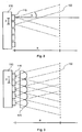
- Système d'impression laser (100) pour éclairer un objet se déplaçant par rapport à un module laser du système d'impression laser (100) dans un plan de travail (180), le module laser comprenant au moins deux réseaux laser (110) de lasers à semi-conducteurs (115) et au moins un élément optique (170), dans lequel l'élément optique (170) est conçu pour imager la lumière laser émise par les réseaux laser (110), de sorte que la lumière laser de lasers à semi-conducteur (115) d'un réseau laser (110) est imagée sur un pixel dans le plan de travail (180) du système d'impression laser (100), et
dans lequel le système d'impression laser est un système d'impression 3D pour la fabrication additive et
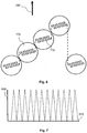
dans lequel deux, trois, quatre ou une multitude de modules laser sont fournis, qui sont agencés en colonnes perpendiculaires à une direction de déplacement (250) de l'objet dans le plan de travail (180), et
dans lequel les colonnes sont en quinconce les unes par rapport aux autres de sorte qu'un premier module laser d'une première colonne de modules laser est conçu pour éclairer une première zone de l'objet et un second module laser d'une seconde colonne de modules laser est conçu pour éclairer une seconde zone de l'objet,
dans lequel la première zone est adjacente à la seconde zone de sorte qu'un éclairage continu de l'objet est rendu possible. - Système d'impression laser (100) selon la revendication 1, dans lequel un élément de zone du pixel est éclairé au moyen d'au moins deux lasers à semi-conducteurs (115).
- Système d'impression laser (100) selon les revendications 1 ou 2, dans lequel l'élément optique (170) est conçu de sorte que les images des réseaux laser (110) se superposent dans le plan de travail (180).
- Système d'impression laser (100) selon les revendications 1 ou 2, dans lequel les réseaux laser (110) du module laser sont agencés en colonnes perpendiculaires à une direction de déplacement (250) de l'objet dans le plan de travail (180), les colonnes sont en quinconce les unes par rapport aux autres de sorte qu'un premier réseau laser (110) d'une première colonne de réseaux laser (110) est conçu pour éclairer une première zone de l'objet et un second réseau laser (110) d'une seconde colonne de réseaux laser (110) est conçu pour éclairer une seconde zone de l'objet, dans lequel la première zone est adjacente à la seconde zone de sorte qu'un éclairage continu de l'objet est rendu possible.
- Système d'impression laser (100) selon l'une des revendications 1 à 4, comprenant au moins un premier et un second module laser agencés côte à côte, chaque module laser comprenant au moins deux réseaux laser (110), dans lequel au moins l'un des deux réseaux laser (110) du premier ou du second module laser est agencé sous la forme d'une source de lumière laser à superposition (117) de sorte qu'en fonctionnement au moins un élément de zone défini dans le plan de travail (180) peut être éclairé par la source de lumière laser à superposition (117) et par un réseau laser distinct (110) du module laser agencé à côté du module laser comprenant la source de lumière laser à superposition (117).
- Système d'impression laser (100) selon la revendication 5, dans lequel l'énergie totale qui est fournie à l'au moins un élément de zone défini de l'objet est telle que sensiblement la même énergie est fournie par élément de zone comme dans le cas de modules laser alignés sans source de lumière laser à superposition (117).
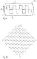
- Système d'impression laser (100) selon la revendication 4, dans lequel l'élément optique (170) associé à un module laser possède un contour externe obtenu à partir d'un contour circulaire ou symétrique en rotation qui est tronqué sur deux côtés opposés et dans lequel les côtés opposés sont alignés l'un par rapport à l'autre le long d'un axe qui est de préférence orienté dans une direction perpendiculaire à la direction de mouvement (250).
- Système d'impression laser (100) selon l'une quelconque des revendications 1 à 7, dans lequel au moins deux lasers à semi-conducteurs (115) d'un réseau laser (110) ou au moins deux sous-groupes de lasers à semi-conducteurs d'un réseau laser (110) sont aptes à être adressés individuellement de sorte qu'une puissance de sortie du réseau laser (110) est apte à être contrôlée par l'extinction d'un ou de plusieurs lasers à semi-conducteurs (115) ou des sous-groupes de lasers à semi-conducteurs.
- Système d'impression laser (100) selon l'une des revendications 1 à 8, comprenant en outre une chambre de traitement (300) comprenant un support pour des couches d'un matériau, dans lequel les modules laser sont agencés dans la chambre de traitement et dans lequel de préférence un dispositif de protection (750) est agencé sur un côté des modules laser qui fait face au support, et dans lequel en outre, de préférence, le dispositif de protection est formé d'au moins une plaque qui est transparente à la lumière laser, de préférence une plaque en verre.
- Système d'impression laser (100) selon la revendication 9, dans lequel un dispositif de régulation de température est fourni, qui régule la température d'au moins la surface du dispositif de protection orientée vers le support.
- Système d'impression laser (100) selon la revendication 10, dans lequel le dispositif de régulation de température est configuré pour chauffer le dispositif de protection de sorte qu'un rayonnement thermique, du matériau dans le plan de travail au dispositif de protection, est sensiblement empêché.
- Système d'impression laser (100) selon l'une quelconque des revendications 1 à 11, dans lequel le système d'impression laser (100) est configuré pour solidifier un matériau couche par couche à des emplacements correspondant à la section transversale d'un article à former dans chaque couche à l'aide des modules laser.
- Système d'impression laser (100) selon l'une quelconque des revendications 1 à 12, dans lequel les modules laser forment une unité d'éclairage (700) et dans lequel l'unité d'éclairage est configurée pour se déplacer sur tout le plan de travail.
- Système d'impression laser selon l'une quelconque des revendications 1 à 13, dans lequel les lasers à semi-conducteur sont des VCSEL (lasers à cavité verticale émettant par la surface), ou dans lequel les lasers à semi-conducteur sont des VECSEL (lasers à cavité verticale externe émettant par la surface).
- Procédé d'impression laser, le procédé comprenant les étapes de- déplacement d'un objet dans un plan de travail (180) par rapport à un module laser ;- émission d'une lumière laser au moyen du module laser comprenant au moins deux réseaux laser (110) de lasers à semi-conducteurs (115) et au moins un élément optique (170) ; et- imagerie de la lumière laser émise par les réseaux laser (110) au moyen de l'élément optique (170), de sorte que la lumière laser des lasers à semi-conducteurs (115) d'un réseau laser (110) est imagée sur un pixel dans le plan de travail (180) ;dans lequel le système d'impression laser (100) est un système d'impression 3D pour la fabrication additive et
dans lequel deux, trois, quatre ou une multitude de modules laser sont utilisés, qui sont agencés en colonnes perpendiculaires à une direction de déplacement (250) de l'objet dans le plan de travail (180),
et dans lequel les colonnes sont en quinconce les unes par rapport aux autres de sorte qu'un premier module laser d'une première colonne de modules laser est conçu pour éclairer une première zone de l'objet et un second module laser d'une seconde colonne de modules laser est conçu pour éclairer une seconde zone de l'objet, dans lequel la première zone est adjacente à la seconde zone de sorte qu'un éclairage continu de l'objet est rendu possible.
Priority Applications (2)
| Application Number | Priority Date | Filing Date | Title |
|---|---|---|---|
| EP14824420.5A EP3079912B1 (fr) | 2013-12-17 | 2014-12-16 | Système d'impression laser |
| EP20165035.5A EP3705300A1 (fr) | 2013-12-17 | 2014-12-16 | Système d'impression laser |
Applications Claiming Priority (3)
| Application Number | Priority Date | Filing Date | Title |
|---|---|---|---|
| EP13197751 | 2013-12-17 | ||
| PCT/EP2014/077967 WO2015091485A1 (fr) | 2013-12-17 | 2014-12-16 | Système d'impression laser |
| EP14824420.5A EP3079912B1 (fr) | 2013-12-17 | 2014-12-16 | Système d'impression laser |
Related Child Applications (1)
| Application Number | Title | Priority Date | Filing Date |
|---|---|---|---|
| EP20165035.5A Division EP3705300A1 (fr) | 2013-12-17 | 2014-12-16 | Système d'impression laser |
Publications (2)
| Publication Number | Publication Date |
|---|---|
| EP3079912A1 EP3079912A1 (fr) | 2016-10-19 |
| EP3079912B1 true EP3079912B1 (fr) | 2020-03-25 |
Family
ID=49886642
Family Applications (3)
| Application Number | Title | Priority Date | Filing Date |
|---|---|---|---|
| EP20165035.5A Pending EP3705300A1 (fr) | 2013-12-17 | 2014-12-16 | Système d'impression laser |
| EP14812255.9A Active EP3083254B1 (fr) | 2013-12-17 | 2014-12-16 | Système d'impression laser |
| EP14824420.5A Active EP3079912B1 (fr) | 2013-12-17 | 2014-12-16 | Système d'impression laser |
Family Applications Before (2)
| Application Number | Title | Priority Date | Filing Date |
|---|---|---|---|
| EP20165035.5A Pending EP3705300A1 (fr) | 2013-12-17 | 2014-12-16 | Système d'impression laser |
| EP14812255.9A Active EP3083254B1 (fr) | 2013-12-17 | 2014-12-16 | Système d'impression laser |
Country Status (10)
| Country | Link |
|---|---|
| US (5) | US10723139B2 (fr) |
| EP (3) | EP3705300A1 (fr) |
| JP (3) | JP6310560B2 (fr) |
| KR (1) | KR102283851B1 (fr) |
| CN (3) | CN105980159B (fr) |
| BR (1) | BR112016013879A2 (fr) |
| ES (1) | ES2799123T3 (fr) |
| MX (1) | MX2016007805A (fr) |
| RU (2) | RU2674511C1 (fr) |
| WO (2) | WO2015091459A1 (fr) |
Families Citing this family (120)
| Publication number | Priority date | Publication date | Assignee | Title |
|---|---|---|---|---|
| GB0816308D0 (en) | 2008-09-05 | 2008-10-15 | Mtt Technologies Ltd | Optical module |
| EP3705300A1 (fr) * | 2013-12-17 | 2020-09-09 | EOS GmbH Electro Optical Systems | Système d'impression laser |
| US10029421B2 (en) * | 2014-09-18 | 2018-07-24 | 3Dm Digital Manufacturing Ltd | Device and a method for 3D printing and manufacturing of materials using quantum cascade lasers |
| DE102015200134A1 (de) * | 2015-01-08 | 2016-07-14 | Trumpf Laser- Und Systemtechnik Gmbh | Modular aufgebaute SLM- oder SLS-Bearbeitungsmaschine |
| US20180056585A1 (en) * | 2015-05-12 | 2018-03-01 | Gizmo 3D Printers | Improvements in 3d printing |
| BR112017025261B8 (pt) * | 2015-05-27 | 2022-08-23 | Landa Labs 2012 Ltd | Dispositivo de imagem |
| JP6505517B2 (ja) * | 2015-06-18 | 2019-04-24 | ローランドディー.ジー.株式会社 | 三次元造形装置 |
| EP3325276B1 (fr) * | 2015-07-23 | 2018-12-12 | Koninklijke Philips N.V. | Système d'impression laser |
| DE102015115810A1 (de) | 2015-09-18 | 2017-03-23 | Osram Opto Semiconductors Gmbh | Optoelektronisches Halbleiterbauteil und 3D-Drucker |
| DE102015219866A1 (de) * | 2015-10-13 | 2017-04-13 | Eos Gmbh Electro Optical Systems | Vorrichtung und Verfahren zum Herstellen eines dreidimensionalen Objekts |
| CN109874321B (zh) | 2015-10-30 | 2021-12-24 | 速尔特技术有限公司 | 增材制造系统和方法 |
| DE102015221623A1 (de) * | 2015-11-04 | 2017-05-04 | Eos Gmbh Electro Optical Systems | Belichteroptik und Vorrichtung zum Herstellen eines dreidimensionalen Objekts |
| CN108463300A (zh) * | 2015-11-16 | 2018-08-28 | 瑞尼斯豪公司 | 用于增材制造设备和方法的模块 |
| US10471543B2 (en) * | 2015-12-15 | 2019-11-12 | Lawrence Livermore National Security, Llc | Laser-assisted additive manufacturing |
| CN108495741B (zh) * | 2016-01-20 | 2020-08-04 | 惠普发展公司,有限责任合伙企业 | 打印设备 |
| US11701819B2 (en) | 2016-01-28 | 2023-07-18 | Seurat Technologies, Inc. | Additive manufacturing, spatial heat treating system and method |
| US11148319B2 (en) | 2016-01-29 | 2021-10-19 | Seurat Technologies, Inc. | Additive manufacturing, bond modifying system and method |
| WO2017187147A1 (fr) * | 2016-04-25 | 2017-11-02 | Renishaw Plc | Procédé d'étalonnage d'une pluralité de dispositifs de balayage dans un appareil de fabrication additive |
| EP3458251A4 (fr) * | 2016-05-17 | 2020-01-08 | Hewlett-Packard Development Company, L.P. | Imprimante 3d à émission de rayonnement de fusion réglée |
| US10717230B2 (en) * | 2016-06-16 | 2020-07-21 | Xerox Corporation | Line laser imager for thermoplastic selective laser sintering |
| KR101787718B1 (ko) * | 2016-06-21 | 2017-11-16 | 한국기계연구원 | 3차원 레이저 프린팅 장치 및 방법 |
| EP3487688B1 (fr) * | 2016-07-20 | 2022-01-26 | Sintratec AG | Elément de protection |
| CN106216862B (zh) * | 2016-07-20 | 2018-10-16 | 华中科技大学 | 一种基于电弧增材和高能束流减材的复合制造方法及装置 |
| US10821717B2 (en) | 2016-07-22 | 2020-11-03 | General Electric Company | Layer orientation control for pixel-based additive manufacturing |
| US10953470B2 (en) | 2016-08-31 | 2021-03-23 | Raytheon Technologies Corporation | Scanning mirror navigation apparatus and method |
| CN106229808B (zh) * | 2016-09-20 | 2023-08-29 | 中国电子科技集团公司第十三研究所 | 脉冲激光器 |
| DE102016218887A1 (de) * | 2016-09-29 | 2018-03-29 | SLM Solutions Group AG | Herstellen dreidimensionaler Werkstücke mittels einer Mehrzahl von Bestrahlungseinheiten |
| JP2018059757A (ja) * | 2016-10-04 | 2018-04-12 | オムロンオートモーティブエレクトロニクス株式会社 | 投光光学系、物体検出装置 |
| DE102016120044A1 (de) | 2016-10-20 | 2018-04-26 | Cl Schutzrechtsverwaltungs Gmbh | Vorrichtung zur additiven Herstellung dreidimensionaler Objekte |
| FR3057794B1 (fr) * | 2016-10-26 | 2019-07-19 | Addup | Perfectionnements a la fabrication additive selective |
| FR3057793B1 (fr) * | 2016-10-26 | 2021-04-09 | Fives Michelin Additive Solutions | Appareil et procede pour fabriquer un objet tridimensionnel |
| US10919285B2 (en) * | 2016-11-07 | 2021-02-16 | General Electric Company | Method and system for x-ray backscatter inspection of additive manufactured parts |
| DE102016222187A1 (de) * | 2016-11-11 | 2018-05-17 | Trumpf Laser- Und Systemtechnik Gmbh | Verfahren zum Bestimmen eines Strahlprofils eines Laserstrahls und Bearbeitungsmaschine |
| DE102016123000B3 (de) * | 2016-11-29 | 2017-12-14 | Scansonic Mi Gmbh | Verfahren zur Überwachung eines Schutzglases und Überwachungsvorrichtung |
| US10399179B2 (en) | 2016-12-14 | 2019-09-03 | General Electric Company | Additive manufacturing systems and methods |
| US10589508B2 (en) * | 2016-12-15 | 2020-03-17 | General Electric Company | Additive manufacturing systems and methods |
| US10583530B2 (en) | 2017-01-09 | 2020-03-10 | General Electric Company | System and methods for fabricating a component with laser array |
| US10549519B2 (en) * | 2017-01-12 | 2020-02-04 | Caterpillar Inc. | Systems and methods for calibrating additive manufacturing operations based on energy density |
| GB201701355D0 (en) | 2017-01-27 | 2017-03-15 | Renishaw Plc | Direct laser writing and chemical etching |
| US11548094B2 (en) | 2017-02-15 | 2023-01-10 | General Electric Company | System and methods for fabricating a component with laser array |
| US10317881B2 (en) | 2017-03-01 | 2019-06-11 | General Electric Company | Parallelized CAD using multi laser additive printing |
| US10695865B2 (en) * | 2017-03-03 | 2020-06-30 | General Electric Company | Systems and methods for fabricating a component with at least one laser device |
| JP6844347B2 (ja) * | 2017-03-15 | 2021-03-17 | 株式会社リコー | レーザ処理装置 |
| US10906132B2 (en) * | 2017-03-31 | 2021-02-02 | General Electric Company | Scan strategies for efficient utilization of laser arrays in direct metal laser melting (DMLM) |
| EP3382828A1 (fr) * | 2017-03-31 | 2018-10-03 | Koninklijke Philips N.V. | Agencement de laser à sécurité intrinsèque comprenant un laser à cavité verticale émettant en surface |
| KR102453653B1 (ko) | 2017-05-11 | 2022-10-11 | 쇠라 테크널러지스 인코포레이티드 | 적층 가공을 위한 패턴화된 광의 스위치야드 빔 라우팅 |
| DE102017210994A1 (de) | 2017-06-28 | 2019-01-03 | Eos Gmbh Electro Optical Systems | Messsystem für eine Vorrichtung zum generativen Herstellen eines dreidimensionalen Objekts |
| WO2019005944A1 (fr) * | 2017-06-28 | 2019-01-03 | 3D Systems, Inc. | Imprimante tridimensionnelle pour la fusion de poudres avec une coloration de surface à l'aide d'un réseau de vcsel |
| US11407034B2 (en) | 2017-07-06 | 2022-08-09 | OmniTek Technology Ltda. | Selective laser melting system and method of using same |
| WO2019022755A1 (fr) * | 2017-07-28 | 2019-01-31 | Hewlett-Packard Development Company, L.P. | Imprimante tridimensionnelle avec dispositif à déplacement |
| GB201712726D0 (en) * | 2017-08-08 | 2017-09-20 | Landa Labs (2012) Ltd | Electric current and heat mitigation in a printing machine writing module |
| US10766242B2 (en) * | 2017-08-24 | 2020-09-08 | General Electric Company | System and methods for fabricating a component using a consolidating device |
| CN107457986A (zh) * | 2017-08-26 | 2017-12-12 | 吴江中瑞机电科技有限公司 | 超高速循环式光固化3d打印机 |
| EP3451470A1 (fr) | 2017-08-30 | 2019-03-06 | Koninklijke Philips N.V. | Dispositif laser comprenant un réseau de vcsel |
| JP6642546B2 (ja) * | 2017-09-21 | 2020-02-05 | 日亜化学工業株式会社 | 波長ビーム結合装置 |
| TWI719261B (zh) * | 2017-09-29 | 2021-02-21 | 國立中興大學 | 利用光學讀寫頭之積層製造裝置 |
| US11084132B2 (en) | 2017-10-26 | 2021-08-10 | General Electric Company | Diode laser fiber array for contour of powder bed fabrication or repair |
| WO2019099928A2 (fr) * | 2017-11-17 | 2019-05-23 | Kevin Friesth | Système de fabrication automatisé avancé et procédés pour composants thermiques et mécaniques utilisant un frittage laser direct hybride quadratique ou au carré, frittage laser métallique direct, commande numérique par ordinateur, pulvérisation thermique, dépôt de métal direct et soudage par friction-malaxage |
| US11027336B2 (en) * | 2017-11-21 | 2021-06-08 | Hamilton Sundstrand Corporation | Splatter shield systems and methods for additive manufacturing |
| CN109940879B (zh) * | 2017-12-20 | 2023-08-29 | 广州中国科学院先进技术研究所 | 一种新型可见光固化3d打印机的控制系统及方法 |
| EP3509170A1 (fr) | 2018-01-05 | 2019-07-10 | Koninklijke Philips N.V. | Agencement de laser économe en énergie |
| CN111356571A (zh) * | 2018-01-16 | 2020-06-30 | 惠普发展公司,有限责任合伙企业 | 三维打印系统 |
| EP3518356A1 (fr) * | 2018-01-24 | 2019-07-31 | Koninklijke Philips N.V. | Agencement de laser avec motif d'émission irrégulier |
| EP3524409A1 (fr) * | 2018-02-09 | 2019-08-14 | CL Schutzrechtsverwaltungs GmbH | Appareil de fabrication additive d'objets tridimensionnels |
| WO2019180960A1 (fr) * | 2018-03-23 | 2019-09-26 | Primetals Technologies Japan株式会社 | Tête d'usinage laser et appareil d'usinage laser, et procédé de réglage de tête d'usinage laser |
| US10875094B2 (en) * | 2018-03-29 | 2020-12-29 | Vulcanforms Inc. | Additive manufacturing systems and methods |
| EP3552806A1 (fr) | 2018-04-09 | 2019-10-16 | Nederlandse Organisatie voor toegepast- natuurwetenschappelijk onderzoek TNO | Procédé d'appareil de formation d'un objet à l'aide de la fabrication additive |
| CN108581215B (zh) * | 2018-05-14 | 2020-01-31 | 苏州米氪激光技术服务有限公司 | 一种双花纹地毯加工用的交错式激光雕刻设备 |
| GB201807830D0 (en) * | 2018-05-15 | 2018-06-27 | Renishaw Plc | Laser beam scanner |
| US20210205892A1 (en) * | 2018-06-08 | 2021-07-08 | Hewlett-Packard Development Company, L.P. | Printing devices |
| EP3588702A1 (fr) * | 2018-06-26 | 2020-01-01 | Koninklijke Philips N.V. | Réseau vcsel à faible retard d'impulsion |
| WO2020014344A1 (fr) | 2018-07-10 | 2020-01-16 | 3D Systems, Inc. | Imprimante tridimensionnelle (3d) avec moteur de lumière à haute résolution |
| WO2020018605A1 (fr) * | 2018-07-16 | 2020-01-23 | Massachusetts Institute Of Technology | Fabrication additive via multiplexage par répartition d'ouverture optique |
| EP3598591A1 (fr) * | 2018-07-17 | 2020-01-22 | Koninklijke Philips N.V. | Arrangement laser à hauteur de construction reduite |
| DE102018211972B4 (de) * | 2018-07-18 | 2020-04-23 | Trumpf Laser Gmbh | Optische Anordnung zur variablen Erzeugung eines Multifoki-Profils, sowie Verfahren zum Betrieb und Verwendung einer solchen Anordnung |
| US11167375B2 (en) | 2018-08-10 | 2021-11-09 | The Research Foundation For The State University Of New York | Additive manufacturing processes and additively manufactured products |
| WO2020091743A1 (fr) * | 2018-10-30 | 2020-05-07 | Hewlett-Packard Development Company, L.P. | Émetteurs d'énergie micro-ondes à pointes |
| KR20200053320A (ko) | 2018-11-08 | 2020-05-18 | 삼성전자주식회사 | 홀로그래픽 디스플레이 장치 |
| DE102018219303A1 (de) | 2018-11-12 | 2020-05-14 | Eos Gmbh Electro Optical Systems | Verzugsoptimiertes Kunststoffpulver |
| DE102018219302A1 (de) | 2018-11-12 | 2020-05-14 | Eos Gmbh Electro Optical Systems | Selektives Sintern von polymerbasiertem Aufbaumaterial |
| KR102130343B1 (ko) * | 2018-11-14 | 2020-08-06 | 한국기계연구원 | 레이저와 분말을 이용한 3차원 형상 제조장치 |
| WO2020121959A1 (fr) * | 2018-12-14 | 2020-06-18 | 株式会社デンソー | Dispositif de mesure de distance optique, dispositif d'émission de lumière laser et son procédé de fabrication |
| JP7172963B2 (ja) * | 2018-12-14 | 2022-11-16 | 株式会社デンソー | 光学的測距装置、レーザ発光装置の製造方法 |
| KR20210104062A (ko) | 2018-12-19 | 2021-08-24 | 쇠라 테크널러지스 인코포레이티드 | 2차원 인쇄를 위해 펄스 변조 레이저를 사용하는 적층 제조 시스템 |
| KR102171814B1 (ko) * | 2018-12-28 | 2020-10-29 | 한국광기술원 | 분할 성형 지원형 광경화 3d 프린터 |
| CA3127485A1 (fr) * | 2019-01-24 | 2020-07-30 | Walter Voit | Systemes, procedes et materiaux pour la fabrication additive a debit ultra-eleve |
| CN111654680A (zh) * | 2019-03-04 | 2020-09-11 | 安世亚太科技股份有限公司 | 一种数字光处理光机的投影拼接方法及装置 |
| DE102019204032B4 (de) * | 2019-03-25 | 2021-09-30 | Fraunhofer-Gesellschaft zur Förderung der angewandten Forschung e.V. | Vorrichtung zur Erzeugung einer räumlich modulierbaren Leistungsdichteverteilung aus Laserstrahlung |
| CN110142406B (zh) * | 2019-03-29 | 2020-05-19 | 西北大学 | 二维光纤面阵高精度激光3d金属打印机及其打印控制方法 |
| CN109986079B (zh) * | 2019-03-29 | 2020-04-14 | 西北大学 | 激光线阵3d金属打印机及其文件转换、打印控制方法 |
| US11230058B2 (en) | 2019-06-07 | 2022-01-25 | The Boeing Company | Additive manufacturing using light source arrays to provide multiple light beams to a build medium via a rotatable reflector |
| US20220194002A1 (en) * | 2019-07-08 | 2022-06-23 | SLM Solutions Group AG | Optical unit and system for producing a three-dimensional workpiece |
| CN110899986B (zh) * | 2019-08-16 | 2022-02-01 | 广东省广袤科技有限公司 | 激光扫描刻蚀制造二维码方法及其装置 |
| CN110412544A (zh) * | 2019-08-23 | 2019-11-05 | 上海禾赛光电科技有限公司 | 激光发射系统以及包括所述激光发射系统的激光雷达 |
| CN110524874B (zh) * | 2019-08-23 | 2022-03-08 | 源秩科技(上海)有限公司 | 光固化3d打印装置及其打印方法 |
| KR102367742B1 (ko) * | 2019-12-10 | 2022-02-25 | (주)캐리마 | 선형광원 장치 및 이를 포함하는 3d프린터 |
| JP7463782B2 (ja) * | 2020-03-17 | 2024-04-09 | 富士フイルムビジネスイノベーション株式会社 | 発光素子アレイ、発光装置、光学装置、計測装置及び情報処理装置 |
| CN111605191A (zh) * | 2020-06-24 | 2020-09-01 | 深圳市智能派科技有限公司 | 一种多尺寸光固化3d打印机拼接光源 |
| US20220062998A1 (en) * | 2020-08-27 | 2022-03-03 | Apple Inc. | Novel architectures for high-throughput additive manufacturing |
| CN113001988B (zh) * | 2021-03-12 | 2021-11-12 | 江苏乾度智造高科技有限公司 | 三维打印装置及方法 |
| IT202100008102A1 (it) | 2021-04-01 | 2021-07-01 | 3D New Tech S R L | Sistema multi laser per additive manufacturing |
| WO2022240397A1 (fr) * | 2021-05-12 | 2022-11-17 | Hewlett-Packard Development Company, L.P. | Quantités de couverture par un agent d'impression |
| IT202100013136A1 (it) | 2021-05-21 | 2021-08-21 | 3D New Tech S R L | Sistema multi laser per additive manufacturing |
| US11951679B2 (en) | 2021-06-16 | 2024-04-09 | General Electric Company | Additive manufacturing system |
| US11599084B2 (en) * | 2021-06-18 | 2023-03-07 | Kyndryl, Inc. | Early notification system of degradation of 3D printed parts |
| US11731367B2 (en) | 2021-06-23 | 2023-08-22 | General Electric Company | Drive system for additive manufacturing |
| US11958250B2 (en) | 2021-06-24 | 2024-04-16 | General Electric Company | Reclamation system for additive manufacturing |
| US11958249B2 (en) | 2021-06-24 | 2024-04-16 | General Electric Company | Reclamation system for additive manufacturing |
| US11826950B2 (en) | 2021-07-09 | 2023-11-28 | General Electric Company | Resin management system for additive manufacturing |
| WO2023287405A1 (fr) * | 2021-07-14 | 2023-01-19 | Hewlett-Packard Development Company, L.P. | Modifications de cellule unitaire |
| DE102021208911A1 (de) | 2021-08-13 | 2023-02-16 | Eos Gmbh Electro Optical Systems | Verbesserung der Positionsgenauigkeit der Energiezufuhr in einer additiven Fertigungsvorrichtung |
| US11827037B2 (en) * | 2021-08-23 | 2023-11-28 | Xerox Corporation | Semiconductor array imager for printing systems |
| US20230056905A1 (en) * | 2021-08-23 | 2023-02-23 | Palo Alto Research Center Incorporated | Independently-addressable high power surface-emitting laser array with tight-pitch packing |
| US20230054034A1 (en) * | 2021-08-23 | 2023-02-23 | Palo Alto Research Center Incorporated | 3d package for semiconductor thermal management |
| US11813799B2 (en) | 2021-09-01 | 2023-11-14 | General Electric Company | Control systems and methods for additive manufacturing |
| WO2023059618A1 (fr) | 2021-10-07 | 2023-04-13 | Additive Monitoring Systems, Llc | Surveillance de la qualité de pièces par lumière structurée en fabrication additive et procédés d'utilisation |
| WO2023075797A1 (fr) * | 2021-10-29 | 2023-05-04 | Hewlett-Packard Development Company, L.P. | Structures flexibles |
| CN114536772B (zh) * | 2022-04-21 | 2022-07-12 | 南京铖联激光科技有限公司 | 3d打印系统中智能分区控制系统及其控制方法 |
| KR20240025737A (ko) * | 2022-08-19 | 2024-02-27 | 한국전자기술연구원 | 열 쏠림 현상 최소화를 위한 공구 경로 패턴 면적에 따른 공구 경로 생성 방법 |
| CN117428210B (zh) * | 2023-12-20 | 2024-03-08 | 中国商用飞机有限责任公司 | 多激光选区熔融搭接方法 |
Family Cites Families (29)
| Publication number | Priority date | Publication date | Assignee | Title |
|---|---|---|---|---|
| US5745153A (en) * | 1992-12-07 | 1998-04-28 | Eastman Kodak Company | Optical means for using diode laser arrays in laser multibeam printers and recorders |
| US5940113A (en) | 1994-12-19 | 1999-08-17 | Xerox Corporation | Lensless printing system with a light bar printhead |
| EP0781661A1 (fr) * | 1995-12-22 | 1997-07-02 | Xerox Corporation | Densité de pixels et vitesse d'impression augmentée dans une imprimante ligne par ligne xérographique avec des séries linéaires multiples de lasers |
| CN1299167A (zh) * | 1999-08-30 | 2001-06-13 | 贝尔-福斯公司 | 通过电阻元件提供插头放电的插座 |
| US6393038B1 (en) * | 1999-10-04 | 2002-05-21 | Sandia Corporation | Frequency-doubled vertical-external-cavity surface-emitting laser |
| US6264981B1 (en) | 1999-10-27 | 2001-07-24 | Anesta Corporation | Oral transmucosal drug dosage using solid solution |
| US6353502B1 (en) | 2000-06-13 | 2002-03-05 | Eastman Kodak Company | VCSEL field correction |
| JP2002019177A (ja) | 2000-07-06 | 2002-01-23 | Seiko Epson Corp | 光プリンタヘッド |
| JP2002316363A (ja) * | 2001-02-16 | 2002-10-29 | Fuji Photo Film Co Ltd | 光造形装置及び露光ユニット |
| DE10111871A1 (de) | 2001-03-13 | 2002-09-19 | Heidelberger Druckmasch Ag | Bebilderungseinrichtung für eine Druckform mit einem Array von VCSEL-Lichtquellen |
| CN100463484C (zh) | 2001-03-29 | 2009-02-18 | 松下电器产业株式会社 | 图像写入装置,光源,光源单元,微透镜以及微透镜的制造方法 |
| JP2003080604A (ja) * | 2001-09-10 | 2003-03-19 | Fuji Photo Film Co Ltd | 積層造形装置 |
| CN1659479A (zh) | 2002-04-10 | 2005-08-24 | 富士胶片株式会社 | 曝光头及曝光装置和它的应用 |
| DE10235434A1 (de) * | 2002-08-02 | 2004-02-12 | Eos Gmbh Electro Optical Systems | Vorrichtung und Verfahren zum Herstellen eins dreidimensionalen Objekts mittels eines generativen Fertigungsverfahrens |
| DE10308708A1 (de) * | 2003-02-28 | 2004-09-09 | Hentze-Lissotschenko Patentverwaltungs Gmbh & Co.Kg | Vorrichtung zur Beaufschlagung eines Objektes mit Laserstrahlung, Bearbeitungsvorrichtung für die Bearbeitung eines Objektes sowie Druckvorrichtung für das Drucken von Bildinformationen |
| US7059530B2 (en) * | 2003-04-24 | 2006-06-13 | Psion Teklogix,Inc. | Heated protective window for an optical scanning device |
| JP2007508596A (ja) | 2003-10-17 | 2007-04-05 | エクスプレイ リミテッド | 投影システムに使用する光学システムおよび方法 |
| US20050151828A1 (en) * | 2004-01-14 | 2005-07-14 | Xerox Corporation. | Xerographic printing system with VCSEL-micro-optic laser printbar |
| US7995084B2 (en) * | 2007-01-25 | 2011-08-09 | Seiko Epson Corporation | Line head and an image forming apparatus using the line head |
| DE202008017990U1 (de) * | 2007-05-30 | 2011-02-10 | Panasonic Electric Works Co., Ltd., Kadoma-shi | Laminier-Formgebungsvorrichtung |
| JP2009056796A (ja) * | 2007-08-07 | 2009-03-19 | Seiko Epson Corp | 露光ヘッド及びそれを用いた画像形成装置 |
| JP2009158709A (ja) * | 2007-12-26 | 2009-07-16 | Seiko Epson Corp | 面発光型半導体レーザアレイおよび面発光型半導体レーザ |
| US8253780B2 (en) | 2008-03-04 | 2012-08-28 | Genie Lens Technology, LLC | 3D display system using a lenticular lens array variably spaced apart from a display screen |
| JP4548497B2 (ja) | 2008-03-04 | 2010-09-22 | カシオ計算機株式会社 | 有機elヘッドおよびそれを用いた印刷装置 |
| US9048633B2 (en) | 2009-08-20 | 2015-06-02 | Koninklijke Philips N.V. | Laser device with configurable intensity distribution |
| JP5944330B2 (ja) * | 2010-03-18 | 2016-07-05 | コーニンクレッカ フィリップス エヌ ヴェKoninklijke Philips N.V. | 印刷装置及び印刷装置を制御する方法 |
| JP2012153029A (ja) * | 2011-01-26 | 2012-08-16 | Fuji Xerox Co Ltd | 露光装置及び画像形成装置 |
| EP3705300A1 (fr) * | 2013-12-17 | 2020-09-09 | EOS GmbH Electro Optical Systems | Système d'impression laser |
| JP7149834B2 (ja) | 2018-12-17 | 2022-10-07 | キヤノン株式会社 | シンチレータの製造方法 |
-
2014
- 2014-12-16 EP EP20165035.5A patent/EP3705300A1/fr active Pending
- 2014-12-16 CN CN201480075736.3A patent/CN105980159B/zh active Active
- 2014-12-16 MX MX2016007805A patent/MX2016007805A/es unknown
- 2014-12-16 CN CN201810337981.7A patent/CN108582769B/zh active Active
- 2014-12-16 US US15/034,963 patent/US10723139B2/en active Active
- 2014-12-16 RU RU2016123826A patent/RU2674511C1/ru active
- 2014-12-16 JP JP2016538064A patent/JP6310560B2/ja active Active
- 2014-12-16 EP EP14812255.9A patent/EP3083254B1/fr active Active
- 2014-12-16 CN CN201480068452.1A patent/CN105829113B/zh active Active
- 2014-12-16 ES ES14824420T patent/ES2799123T3/es active Active
- 2014-12-16 WO PCT/EP2014/077931 patent/WO2015091459A1/fr active Application Filing
- 2014-12-16 KR KR1020167015838A patent/KR102283851B1/ko active IP Right Grant
- 2014-12-16 BR BR112016013879A patent/BR112016013879A2/pt not_active Application Discontinuation
- 2014-12-16 WO PCT/EP2014/077967 patent/WO2015091485A1/fr active Application Filing
- 2014-12-16 RU RU2016128798A patent/RU2656205C1/ru not_active IP Right Cessation
- 2014-12-16 JP JP2016539227A patent/JP6585597B2/ja active Active
- 2014-12-16 EP EP14824420.5A patent/EP3079912B1/fr active Active
- 2014-12-16 US US15/103,888 patent/US10518555B2/en active Active
-
2019
- 2019-06-27 JP JP2019119534A patent/JP6810199B2/ja active Active
-
2020
- 2020-06-16 US US16/902,675 patent/US11260583B2/en active Active
-
2022
- 2022-01-21 US US17/581,046 patent/US11858204B2/en active Active
-
2023
- 2023-11-20 US US18/514,899 patent/US20240083109A1/en active Pending
Non-Patent Citations (1)
| Title |
|---|
| None * |
Also Published As
Similar Documents
| Publication | Publication Date | Title |
|---|---|---|
| US11260583B2 (en) | Laser printing system | |
| US11203149B2 (en) | Three-dimensional modeling apparatus, object, and method of manufacturing an object | |
| JP2017501052A5 (fr) | ||
| EP2404220B1 (fr) | Système d'éclairage pour une utilisation dans un appareil de stéréolithographie | |
| JP5944330B2 (ja) | 印刷装置及び印刷装置を制御する方法 | |
| JP2013527809A5 (fr) | ||
| US10996653B2 (en) | Three-dimensional object building device, three-dimensional object building method, and method of producing three-dimensional object | |
| EP3807719A1 (fr) | Agencement d'exposition pour un système de fabrication additive, système de fabrication additive et procédé de fabrication d'un objet | |
| EP0974470B1 (fr) | Tête d'écriture et imprimante optique |
Legal Events
| Date | Code | Title | Description |
|---|---|---|---|
| PUAI | Public reference made under article 153(3) epc to a published international application that has entered the european phase |
Free format text: ORIGINAL CODE: 0009012 |
|
| 17P | Request for examination filed |
Effective date: 20160715 |
|
| AK | Designated contracting states |
Kind code of ref document: A1 Designated state(s): AL AT BE BG CH CY CZ DE DK EE ES FI FR GB GR HR HU IE IS IT LI LT LU LV MC MK MT NL NO PL PT RO RS SE SI SK SM TR |
|
| AX | Request for extension of the european patent |
Extension state: BA ME |
|
| DAX | Request for extension of the european patent (deleted) | ||
| STAA | Information on the status of an ep patent application or granted ep patent |
Free format text: STATUS: EXAMINATION IS IN PROGRESS |
|
| 17Q | First examination report despatched |
Effective date: 20190221 |
|
| GRAP | Despatch of communication of intention to grant a patent |
Free format text: ORIGINAL CODE: EPIDOSNIGR1 |
|
| STAA | Information on the status of an ep patent application or granted ep patent |
Free format text: STATUS: GRANT OF PATENT IS INTENDED |
|
| INTG | Intention to grant announced |
Effective date: 20191015 |
|
| GRAS | Grant fee paid |
Free format text: ORIGINAL CODE: EPIDOSNIGR3 |
|
| GRAA | (expected) grant |
Free format text: ORIGINAL CODE: 0009210 |
|
| STAA | Information on the status of an ep patent application or granted ep patent |
Free format text: STATUS: THE PATENT HAS BEEN GRANTED |
|
| AK | Designated contracting states |
Kind code of ref document: B1 Designated state(s): AL AT BE BG CH CY CZ DE DK EE ES FI FR GB GR HR HU IE IS IT LI LT LU LV MC MK MT NL NO PL PT RO RS SE SI SK SM TR |
|
| REG | Reference to a national code |
Ref country code: GB Ref legal event code: FG4D |
|
| REG | Reference to a national code |
Ref country code: AT Ref legal event code: REF Ref document number: 1248125 Country of ref document: AT Kind code of ref document: T Effective date: 20200415 Ref country code: IE Ref legal event code: FG4D |
|
| REG | Reference to a national code |
Ref country code: DE Ref legal event code: R096 Ref document number: 602014062910 Country of ref document: DE |
|
| REG | Reference to a national code |
Ref country code: NL Ref legal event code: FP |
|
| REG | Reference to a national code |
Ref country code: SE Ref legal event code: TRGR Ref country code: CH Ref legal event code: NV Representative=s name: FREIGUTPARTNERS GMBH, CH |
|
| PG25 | Lapsed in a contracting state [announced via postgrant information from national office to epo] |
Ref country code: RS Free format text: LAPSE BECAUSE OF FAILURE TO SUBMIT A TRANSLATION OF THE DESCRIPTION OR TO PAY THE FEE WITHIN THE PRESCRIBED TIME-LIMIT Effective date: 20200325 Ref country code: NO Free format text: LAPSE BECAUSE OF FAILURE TO SUBMIT A TRANSLATION OF THE DESCRIPTION OR TO PAY THE FEE WITHIN THE PRESCRIBED TIME-LIMIT Effective date: 20200625 Ref country code: FI Free format text: LAPSE BECAUSE OF FAILURE TO SUBMIT A TRANSLATION OF THE DESCRIPTION OR TO PAY THE FEE WITHIN THE PRESCRIBED TIME-LIMIT Effective date: 20200325 |
|
| PG25 | Lapsed in a contracting state [announced via postgrant information from national office to epo] |
Ref country code: LV Free format text: LAPSE BECAUSE OF FAILURE TO SUBMIT A TRANSLATION OF THE DESCRIPTION OR TO PAY THE FEE WITHIN THE PRESCRIBED TIME-LIMIT Effective date: 20200325 Ref country code: GR Free format text: LAPSE BECAUSE OF FAILURE TO SUBMIT A TRANSLATION OF THE DESCRIPTION OR TO PAY THE FEE WITHIN THE PRESCRIBED TIME-LIMIT Effective date: 20200626 Ref country code: HR Free format text: LAPSE BECAUSE OF FAILURE TO SUBMIT A TRANSLATION OF THE DESCRIPTION OR TO PAY THE FEE WITHIN THE PRESCRIBED TIME-LIMIT Effective date: 20200325 Ref country code: BG Free format text: LAPSE BECAUSE OF FAILURE TO SUBMIT A TRANSLATION OF THE DESCRIPTION OR TO PAY THE FEE WITHIN THE PRESCRIBED TIME-LIMIT Effective date: 20200625 |
|
| REG | Reference to a national code |
Ref country code: LT Ref legal event code: MG4D |
|
| PG25 | Lapsed in a contracting state [announced via postgrant information from national office to epo] |
Ref country code: SM Free format text: LAPSE BECAUSE OF FAILURE TO SUBMIT A TRANSLATION OF THE DESCRIPTION OR TO PAY THE FEE WITHIN THE PRESCRIBED TIME-LIMIT Effective date: 20200325 Ref country code: EE Free format text: LAPSE BECAUSE OF FAILURE TO SUBMIT A TRANSLATION OF THE DESCRIPTION OR TO PAY THE FEE WITHIN THE PRESCRIBED TIME-LIMIT Effective date: 20200325 Ref country code: IS Free format text: LAPSE BECAUSE OF FAILURE TO SUBMIT A TRANSLATION OF THE DESCRIPTION OR TO PAY THE FEE WITHIN THE PRESCRIBED TIME-LIMIT Effective date: 20200725 Ref country code: SK Free format text: LAPSE BECAUSE OF FAILURE TO SUBMIT A TRANSLATION OF THE DESCRIPTION OR TO PAY THE FEE WITHIN THE PRESCRIBED TIME-LIMIT Effective date: 20200325 Ref country code: RO Free format text: LAPSE BECAUSE OF FAILURE TO SUBMIT A TRANSLATION OF THE DESCRIPTION OR TO PAY THE FEE WITHIN THE PRESCRIBED TIME-LIMIT Effective date: 20200325 Ref country code: PT Free format text: LAPSE BECAUSE OF FAILURE TO SUBMIT A TRANSLATION OF THE DESCRIPTION OR TO PAY THE FEE WITHIN THE PRESCRIBED TIME-LIMIT Effective date: 20200818 Ref country code: CZ Free format text: LAPSE BECAUSE OF FAILURE TO SUBMIT A TRANSLATION OF THE DESCRIPTION OR TO PAY THE FEE WITHIN THE PRESCRIBED TIME-LIMIT Effective date: 20200325 Ref country code: LT Free format text: LAPSE BECAUSE OF FAILURE TO SUBMIT A TRANSLATION OF THE DESCRIPTION OR TO PAY THE FEE WITHIN THE PRESCRIBED TIME-LIMIT Effective date: 20200325 |
|
| REG | Reference to a national code |
Ref country code: AT Ref legal event code: UEP Ref document number: 1248125 Country of ref document: AT Kind code of ref document: T Effective date: 20200325 |
|
| REG | Reference to a national code |
Ref country code: ES Ref legal event code: FG2A Ref document number: 2799123 Country of ref document: ES Kind code of ref document: T3 Effective date: 20201214 |
|
| REG | Reference to a national code |
Ref country code: DE Ref legal event code: R097 Ref document number: 602014062910 Country of ref document: DE |
|
| PG25 | Lapsed in a contracting state [announced via postgrant information from national office to epo] |
Ref country code: DK Free format text: LAPSE BECAUSE OF FAILURE TO SUBMIT A TRANSLATION OF THE DESCRIPTION OR TO PAY THE FEE WITHIN THE PRESCRIBED TIME-LIMIT Effective date: 20200325 |
|
| PLBE | No opposition filed within time limit |
Free format text: ORIGINAL CODE: 0009261 |
|
| STAA | Information on the status of an ep patent application or granted ep patent |
Free format text: STATUS: NO OPPOSITION FILED WITHIN TIME LIMIT |
|
| PG25 | Lapsed in a contracting state [announced via postgrant information from national office to epo] |
Ref country code: PL Free format text: LAPSE BECAUSE OF FAILURE TO SUBMIT A TRANSLATION OF THE DESCRIPTION OR TO PAY THE FEE WITHIN THE PRESCRIBED TIME-LIMIT Effective date: 20200325 |
|
| 26N | No opposition filed |
Effective date: 20210112 |
|
| PG25 | Lapsed in a contracting state [announced via postgrant information from national office to epo] |
Ref country code: SI Free format text: LAPSE BECAUSE OF FAILURE TO SUBMIT A TRANSLATION OF THE DESCRIPTION OR TO PAY THE FEE WITHIN THE PRESCRIBED TIME-LIMIT Effective date: 20200325 |
|
| PG25 | Lapsed in a contracting state [announced via postgrant information from national office to epo] |
Ref country code: MC Free format text: LAPSE BECAUSE OF FAILURE TO SUBMIT A TRANSLATION OF THE DESCRIPTION OR TO PAY THE FEE WITHIN THE PRESCRIBED TIME-LIMIT Effective date: 20200325 |
|
| REG | Reference to a national code |
Ref country code: BE Ref legal event code: MM Effective date: 20201231 |
|
| PG25 | Lapsed in a contracting state [announced via postgrant information from national office to epo] |
Ref country code: IE Free format text: LAPSE BECAUSE OF NON-PAYMENT OF DUE FEES Effective date: 20201216 Ref country code: LU Free format text: LAPSE BECAUSE OF NON-PAYMENT OF DUE FEES Effective date: 20201216 |
|
| PG25 | Lapsed in a contracting state [announced via postgrant information from national office to epo] |
Ref country code: TR Free format text: LAPSE BECAUSE OF FAILURE TO SUBMIT A TRANSLATION OF THE DESCRIPTION OR TO PAY THE FEE WITHIN THE PRESCRIBED TIME-LIMIT Effective date: 20200325 Ref country code: MT Free format text: LAPSE BECAUSE OF FAILURE TO SUBMIT A TRANSLATION OF THE DESCRIPTION OR TO PAY THE FEE WITHIN THE PRESCRIBED TIME-LIMIT Effective date: 20200325 Ref country code: CY Free format text: LAPSE BECAUSE OF FAILURE TO SUBMIT A TRANSLATION OF THE DESCRIPTION OR TO PAY THE FEE WITHIN THE PRESCRIBED TIME-LIMIT Effective date: 20200325 |
|
| PG25 | Lapsed in a contracting state [announced via postgrant information from national office to epo] |
Ref country code: MK Free format text: LAPSE BECAUSE OF FAILURE TO SUBMIT A TRANSLATION OF THE DESCRIPTION OR TO PAY THE FEE WITHIN THE PRESCRIBED TIME-LIMIT Effective date: 20200325 Ref country code: AL Free format text: LAPSE BECAUSE OF FAILURE TO SUBMIT A TRANSLATION OF THE DESCRIPTION OR TO PAY THE FEE WITHIN THE PRESCRIBED TIME-LIMIT Effective date: 20200325 |
|
| PG25 | Lapsed in a contracting state [announced via postgrant information from national office to epo] |
Ref country code: BE Free format text: LAPSE BECAUSE OF NON-PAYMENT OF DUE FEES Effective date: 20201231 |
|
| PGFP | Annual fee paid to national office [announced via postgrant information from national office to epo] |
Ref country code: ES Payment date: 20230227 Year of fee payment: 9 Ref country code: CH Payment date: 20230103 Year of fee payment: 9 |
|
| P01 | Opt-out of the competence of the unified patent court (upc) registered |
Effective date: 20230525 |
|
| PGFP | Annual fee paid to national office [announced via postgrant information from national office to epo] |
Ref country code: GB Payment date: 20231220 Year of fee payment: 10 |
|
| PGFP | Annual fee paid to national office [announced via postgrant information from national office to epo] |
Ref country code: SE Payment date: 20231220 Year of fee payment: 10 Ref country code: NL Payment date: 20231220 Year of fee payment: 10 Ref country code: IT Payment date: 20231228 Year of fee payment: 10 Ref country code: FR Payment date: 20231221 Year of fee payment: 10 Ref country code: DE Payment date: 20231214 Year of fee payment: 10 Ref country code: AT Payment date: 20231221 Year of fee payment: 10 |
|
| PGFP | Annual fee paid to national office [announced via postgrant information from national office to epo] |
Ref country code: ES Payment date: 20240129 Year of fee payment: 10 |