EP3075079B1 - Fast adc for optical tape wobble signal - Google Patents
Fast adc for optical tape wobble signal Download PDFInfo
- Publication number
- EP3075079B1 EP3075079B1 EP14790410.6A EP14790410A EP3075079B1 EP 3075079 B1 EP3075079 B1 EP 3075079B1 EP 14790410 A EP14790410 A EP 14790410A EP 3075079 B1 EP3075079 B1 EP 3075079B1
- Authority
- EP
- European Patent Office
- Prior art keywords
- signal
- wobble signal
- output signal
- converter
- output
- Prior art date
- Legal status (The legal status is an assumption and is not a legal conclusion. Google has not performed a legal analysis and makes no representation as to the accuracy of the status listed.)
- Active
Links
Images


Classifications
-
- G—PHYSICS
- G11—INFORMATION STORAGE
- G11B—INFORMATION STORAGE BASED ON RELATIVE MOVEMENT BETWEEN RECORD CARRIER AND TRANSDUCER
- G11B20/00—Signal processing not specific to the method of recording or reproducing; Circuits therefor
- G11B20/10—Digital recording or reproducing
- G11B20/10009—Improvement or modification of read or write signals
- G11B20/10305—Improvement or modification of read or write signals signal quality assessment
- G11B20/10342—Improvement or modification of read or write signals signal quality assessment sub-information or auxiliary signals different from the normal recording marks, e.g. signals reproduced from wobble tracks
-
- H—ELECTRICITY
- H03—ELECTRONIC CIRCUITRY
- H03M—CODING; DECODING; CODE CONVERSION IN GENERAL
- H03M3/00—Conversion of analogue values to or from differential modulation
- H03M3/02—Delta modulation, i.e. one-bit differential modulation
-
- G—PHYSICS
- G11—INFORMATION STORAGE
- G11B—INFORMATION STORAGE BASED ON RELATIVE MOVEMENT BETWEEN RECORD CARRIER AND TRANSDUCER
- G11B7/00—Recording or reproducing by optical means, e.g. recording using a thermal beam of optical radiation by modifying optical properties or the physical structure, reproducing using an optical beam at lower power by sensing optical properties; Record carriers therefor
- G11B7/004—Recording, reproducing or erasing methods; Read, write or erase circuits therefor
- G11B7/005—Reproducing
- G11B7/0053—Reproducing non-user data, e.g. wobbled address, prepits, BCA
-
- G—PHYSICS
- G11—INFORMATION STORAGE
- G11B—INFORMATION STORAGE BASED ON RELATIVE MOVEMENT BETWEEN RECORD CARRIER AND TRANSDUCER
- G11B7/00—Recording or reproducing by optical means, e.g. recording using a thermal beam of optical radiation by modifying optical properties or the physical structure, reproducing using an optical beam at lower power by sensing optical properties; Record carriers therefor
- G11B7/002—Recording, reproducing or erasing systems characterised by the shape or form of the carrier
- G11B7/003—Recording, reproducing or erasing systems characterised by the shape or form of the carrier with webs, filaments or wires, e.g. belts, spooled tapes or films of quasi-infinite extent
Definitions
- the present invention is related to methods and apparatuses for digitizing an analog signal, and in particular, an analog wobble signal.
- Servo systems in optical data recording devices such as optical tape drives utilize tracking error signals, detected from the optical media via an optical pickup unit (OPU) device, to accurately record and then retrieve data on the optical media.
- OPU optical pickup unit
- Figures 1 and 2 illustrate a portion of a typical optical recording medium.
- Figure 1 is a top view while Figure 2 is a side view.
- Optical data storage medium 10 includes a nanostructure surface relief pattern embossed on the surface of the optical medium.
- the nanostructure includes lands 12 and grooves 14 embossed in the Z direction (i.e., parallel to the face of optical data storage medium 10) thereon in a preformatting process.
- These surface relief patterns are used to generate the tracking signals used by a servo system to track the position of an optical head reading or writing to the medium.
- An optical drive OPU with the aid of electronic signal processing generates a tracking error signal (TES) from the detected patterns.
- TES tracking error signal
- the edges of these embossed lands 12 and grooves 14 relief patterns are structurally modulated in the horizontal directions parallel to the face of optical recording data storage 10 (e.g., Y axes to track X axes) with sinusoidal patterns 16 (i.e., wobbles) which contain individual track address codes.
- sinusoidal patterns 16 i.e., wobbles
- These wobble patterns embedded (or embossed) on the surface of optical data storage media such as optical tape, during media pre-formatting process, and thereafter detected by the optical read element during normal operation of the data storage devices are the essential part of reliable data recording and retrieval functionality of the these devices.
- Figure 1 also depicts recording marks 18 encoded thereon.
- FIG. 1 A technique referred to as “Radial Push Pull” Tracking signal generation (also referred to as “Main Push Pull” (MPP)), have been conventionally used to generate the Tracking Error Signal (TES) for the rewritable optical recording media preformatted with "land” and “groove” track geometries as set forth above.
- This scheme generates a reference tracking signal based on the geometries of land and grooved tracks on the media and detectable by a main quad photodetector (QPD) of the OPU.
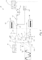
- Figure 3 provides a schematic illustration of a typical signal processing scheme for the TES signal generated by the QPD.
- Signal processing system 20 includes recording/reading head 21.
- Recording/reading head 21 includes quad photodetector 22 which includes individual photodetectors 24, 26, 28, and 30. Signals 32, 34, 36, 38 from photodetectors 24, 26, 28, 30 are amplified by amplifiers 42, 44, 46, 48 to provide signals 52, 54, 56, 58. Signals 52, 54 are provided to adder 60 which outputs summed signal 62. Signals 56, 58 are provided to adder 64 which outputs summed signal 66. Summed signal 62 and summed signal 66 are inputted into subtractor circuit 70 with outputs difference signal 72 which is further processed to provide TES signal 78 and wobble signal 80.
- low pass filter 82 receives difference signal 72 as an input and outputs TES signal 78 while band pass filter 84 receives difference signal 72 and outputs wobble signal 80.
- the high frequency wobble signal includes, among other information, the key data track ID and Address codes.
- TES signal 78 and wobble signal 80 are used by recording/reading head servo system 86 to provide positioning information regarding the position of head 21.
- digital servo systems control the dynamic operation of the OPUs by using wobble signal information to place the OPU on the correct desired data track. Additional methods for detecting wobble signals and/or Tracking Error Signals are set forth in U.S. Pat. Nos. 5,383,169 ; 6,009059 ; and 6,937,542 ; the entire disclosures of which are hereby incorporated by reference.
- the present invention concerns an analog-to-digital converter according to claim 1 and a corresponding method using an analog-to-digital converter according to claim 14.
- the present invention solves one or more problems of the prior art by providing in at least one embodiment a mixed signal analog-to-digital converter for digitizing an optical wobble signal.
- the analog-to-digital converter includes a feedback loop that receives the wobble signal having a wobble signal frequency.
- the feedback loop includes a comparator that receives the wobble signal through a first resistive component at a first comparator input and outputs a first output signal having either a high output or a low output.
- the feedback loop also includes a sampling component that samples the first output signal at a sampling frequency and outputs a second output signal.
- the sampling frequency is at least 50 times greater than the wobble signal frequency.
- the feedback loop also includes a first integrator component that receives the second output signal and outputs a third output signal.
- the output signal is provided to the first comparator input through a second resistive component such that the third output signal tracks the wobble signal due to feedback action in the feedback loop.
- the analog-to-digital converter further includes a final discrete integrator component that integrates the second output signal to provide a digital representation of the wobble signal.
- the mixed signal analog-to-digital converter of the present embodiment provides a low cost, low component ADC to be used in optical storage devices.
- a method for digitizing an optical tape wobble signal having a wobble signal frequency is provided.
- the method is performed by the analog-to-digital converter set forth above.
- the method includes a step of applying the wobble signal to a comparator at a first comparator input through a first resistive component.
- the comparator outputs a first output signal that is either high or low.
- the first output signal is sampled at a sampling frequency such that a second output signal is outputted. Characteristically, the sampling frequency is at least 50 times greater than the wobble signal frequency.
- the second output signal is integrated to form a third output signal.
- the third output signal is provided to the first comparator input through a second resistive component such that the third output signal tracks the wobble signal due to a feedback loop.
- the second output signal is integrated to provide a digital representation of the wobble signal.
- Analog-to-digital converter 90 includes feedback loop 92 that receives wobble signal 94 having a wobble signal frequency.
- the wobble signal frequency is from 0.5 megahertz to 10 megahertz.
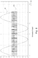
- Figure 5 provides a plot of a typical wobble signal which is inputted to analog-to-digital converter 90.
- wobble signal 94 is generated from a wobble detection system such as the prior art system depicted in Figure 2 .
- feedback loop 92 includes comparator 100 which includes an operational amplifier.
- Comparator 100 typically includes non-inverting input 102 and inverting input 104.
- Comparator 100 receives wobble signal 94 through first resistive component 106 at a first comparator input (e.g., non-inverting input 102).
- First resistive component 106 incudes one or more resistors.
- a reference voltage e.g., ground or zero volts
- Comparator 100 outputs first signal output 110 which is a logical two level signal alternating between a high output value or a low output value.
- pull-up resistor 112 is used to ensure that the output switches between the high value V logic and a low value (e.g., 0 volts).
- the high value and low value allow binary encoding of the output.
- Figure 6 provides a plot of first signal output 110 with the corresponding wobble signal also plotted.
- feedback loop 92 also includes sampling component 114 that samples the first output signal 110 at a sampling frequency and outputs second output signal 116.
- sampling component 114 includes a transistor switch driven by a control signal operating at the sampling frequency received from clock 115, and in particular, a MOSFET transistor switch. It should also be appreciated that sampling component 114 may also be programmed into a field-programmable gate array (FPGA) 118 as set forth below.
- FPGA field-programmable gate array
- the sampling frequency is at least 50 times greater than the wobble signal frequency.
- the sampling frequency is at least 100 times greater than the wobble signal frequency.
- the sampling frequency is from about 50 to about 1000 times the wobble signal frequency.
- Feedback loop 92 also includes first integrator component 120 that receives the second output signal 116 while outputting and outputs a third output signal 122.
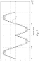
- Figure 7 provides a plot of the output of first integrator component 120.
- first integrator 120 is an operational amplifier integrator.
- the first integrator includes operational amplifier 124 having non-inverting input 126 and inverting input 128 such that second output signal 116 is provided inverting input 128 via resistor 130.
- Capacitor 132 electrically connects inverting input 128 to output 134 of operational amplifier 124.
- a voltage derived from voltage divider 136 is provided to non-inverting input 126.
- Third output signal 122 is provided to comparator input 102 through second resistive component 140 such that the third output signal tracks the wobble signal due to feedback action in the feedback loop 92.
- second resistive component 140 includes one or more resistors.
- the high bandwidth feedback control law of feedback loop 92 enforces the accurate pattern matching of the wobble signal 94 and third output signal 122.
- integrator action in the feedback path of the loop provides signal differentiation in the forward path.
- a level shifter 142 shifts the second signal by a voltage offset prior to the second signal being received by the final integrator.
- the analog-to-digital converter 90 further includes final discrete integrator component 144 that reconstructs second output signal 116 in the discrete domain to provide a digital representation of the wobble signal as fourth signal 146.
- final discrete integrator component 144 is a low pass filter, and in particular, an infinite impulse response (IIR) filter.
- Figure 8 provides a plot of an example with signal 146 overlaying an input wobble signal.
- a field-programmable gate array (FPGA) 118 includes sampling component 114, level shifter 142, and final discrete integrator component 144.
- step a a wobble signal 94 is applied to a comparator at a first comparator input through a first resistive component.
- the comparator outputs first output signal 110 which alternates between a high output voltage value or a low output voltage value as set forth above.
- step b) first output signal 110 is sampled at a sampling frequency such that a second output signal 116 is outputted. Characteristically, the sampling frequency is at least 50 times greater than the wobble signal frequency as set forth above.
- step c) second output signal is integrated to form third output signal122.
- the third output signal is provided to the first comparator input through a second resistive component such that the third output signal tracks the wobble signal due to a feedback loop 92.
- the second output signal is integrated to provide a digital representation 146 of the wobble signal.
Landscapes
- Engineering & Computer Science (AREA)
- Theoretical Computer Science (AREA)
- Signal Processing (AREA)
- Optical Recording Or Reproduction (AREA)
- Analogue/Digital Conversion (AREA)
- Signal Processing For Digital Recording And Reproducing (AREA)
Applications Claiming Priority (2)
| Application Number | Priority Date | Filing Date | Title |
|---|---|---|---|
| US14/090,249 US8923104B1 (en) | 2013-11-26 | 2013-11-26 | Fast ADC for optical tape wobble signal |
| PCT/US2014/058809 WO2015080801A1 (en) | 2013-11-26 | 2014-10-02 | Fast adc for optical tape wobble signal |
Publications (2)
| Publication Number | Publication Date |
|---|---|
| EP3075079A1 EP3075079A1 (en) | 2016-10-05 |
| EP3075079B1 true EP3075079B1 (en) | 2021-07-07 |
Family
ID=51830608
Family Applications (1)
| Application Number | Title | Priority Date | Filing Date |
|---|---|---|---|
| EP14790410.6A Active EP3075079B1 (en) | 2013-11-26 | 2014-10-02 | Fast adc for optical tape wobble signal |
Country Status (7)
| Country | Link |
|---|---|
| US (1) | US8923104B1 (OSRAM) |
| EP (1) | EP3075079B1 (OSRAM) |
| JP (1) | JP6419799B2 (OSRAM) |
| CN (1) | CN105594127B (OSRAM) |
| AU (1) | AU2014355139B2 (OSRAM) |
| NZ (1) | NZ717999A (OSRAM) |
| WO (1) | WO2015080801A1 (OSRAM) |
Families Citing this family (1)
| Publication number | Priority date | Publication date | Assignee | Title |
|---|---|---|---|---|
| US10484002B1 (en) * | 2018-12-27 | 2019-11-19 | Keithley Instruments, Llc | High-speed high-resolution digital-to-analog converter |
Family Cites Families (24)
| Publication number | Priority date | Publication date | Assignee | Title |
|---|---|---|---|---|
| KR950010418B1 (ko) | 1991-08-28 | 1995-09-16 | 미쯔비시덴끼 가부시끼가이샤 | 광기록재생장치 |
| JPH08265163A (ja) * | 1995-03-24 | 1996-10-11 | Ricoh Co Ltd | 信号処理装置 |
| JPH1069640A (ja) | 1996-08-27 | 1998-03-10 | Mitsumi Electric Co Ltd | Cd−rドライブにおけるウォブル信号生成方法 |
| JP3503513B2 (ja) | 1999-02-22 | 2004-03-08 | ヤマハ株式会社 | 光ディスク記録方法及び装置 |
| JP2001053586A (ja) * | 1999-08-06 | 2001-02-23 | Mitsubishi Electric Corp | 積分回路およびa/d変換回路ならびに積分方法 |
| JP3956582B2 (ja) * | 2000-05-30 | 2007-08-08 | ヤマハ株式会社 | A/d変換回路 |
| US7142486B2 (en) * | 2001-04-02 | 2006-11-28 | Ricoh Company, Ltd. | Signal processing method and signal processing apparatus |
| JP2003243986A (ja) * | 2002-02-20 | 2003-08-29 | Tadahiro Omi | A/d変換装置 |
| JP3975111B2 (ja) * | 2002-04-19 | 2007-09-12 | 松下電器産業株式会社 | 混合型変調器、オーバーサンプリング型d/a変換器およびa/d変換器 |
| WO2005015548A2 (ja) * | 2003-08-07 | 2005-02-17 | Matsushita Electric Industrial Co Ltd | 光ディスク装置 |
| JP3597189B1 (ja) * | 2003-10-09 | 2004-12-02 | 株式会社リコー | ウォブル信号復調方法、ウォブル信号復調回路及び光ディスク装置 |
| JP2005158239A (ja) * | 2003-10-27 | 2005-06-16 | Matsushita Electric Ind Co Ltd | 光ディスク装置、クロック信号生成方法、プログラムおよび制御装置 |
| JP4277781B2 (ja) * | 2004-11-04 | 2009-06-10 | 日本ビクター株式会社 | 光ディスクドライブ装置のアドレス情報検出回路 |
| KR100640658B1 (ko) * | 2005-07-29 | 2006-11-01 | 삼성전자주식회사 | 블루-레이 디스크 드라이브에서 시간 변화량를 이용하여hmw 신호를 검출하는 장치 및 방법 |
| US20070064566A1 (en) * | 2005-09-21 | 2007-03-22 | Wei-Hsin Hsu | Signal process device and method for obtaining wobble signal |
| US8355302B1 (en) * | 2006-05-11 | 2013-01-15 | Marvell International Ltd. | Offset loop for wobble |
| US20080080332A1 (en) * | 2006-09-29 | 2008-04-03 | Media Tek Inc. | Recording medium type identification method and device |
| JP4852021B2 (ja) * | 2007-11-15 | 2012-01-11 | 株式会社東芝 | 増幅装置 |
| JP4407747B2 (ja) * | 2007-12-13 | 2010-02-03 | ソニー株式会社 | A/d変換器及び情報記録再生装置 |
| JP4525746B2 (ja) * | 2007-12-13 | 2010-08-18 | ソニー株式会社 | ウォブル信号抽出回路及び光ディスク装置 |
| JP2009158035A (ja) * | 2007-12-27 | 2009-07-16 | Canon Inc | 光ディスク記録再生装置 |
| KR101466926B1 (ko) * | 2008-09-25 | 2014-12-01 | 삼성전자주식회사 | 오프셋 전압을 보상할 수 있는 신호 처리기, 워블 신호 검출기, 및 이를 포함하는 광 디스크 장치 |
| WO2010073450A1 (ja) * | 2008-12-25 | 2010-07-01 | パナソニック株式会社 | 信号処理回路および光ディスク再生装置 |
| JP2011233192A (ja) * | 2010-04-26 | 2011-11-17 | Renesas Electronics Corp | 半導体集積回路およびそれを搭載した光ディスク装置 |
-
2013
- 2013-11-26 US US14/090,249 patent/US8923104B1/en active Active
-
2014
- 2014-10-02 CN CN201480054216.4A patent/CN105594127B/zh active Active
- 2014-10-02 AU AU2014355139A patent/AU2014355139B2/en active Active
- 2014-10-02 NZ NZ717999A patent/NZ717999A/en unknown
- 2014-10-02 EP EP14790410.6A patent/EP3075079B1/en active Active
- 2014-10-02 WO PCT/US2014/058809 patent/WO2015080801A1/en not_active Ceased
- 2014-10-02 JP JP2016521762A patent/JP6419799B2/ja active Active
Non-Patent Citations (1)
| Title |
|---|
| HARVEY B: "DELTA MODULATORS SIMPLIFY A/D CONVERSION", EDN ELECTRICAL DESIGN NEWS.(TEXAS INSTRUMENT), REED BUSINESS INFORMATION, HIGHLANDS RANCH, CO, US, vol. 34, no. 13, 22 June 1989 (1989-06-22), pages 175 - 182,184, XP000111366, ISSN: 0012-7515 * |
Also Published As
| Publication number | Publication date |
|---|---|
| AU2014355139B2 (en) | 2018-07-12 |
| JP2017504141A (ja) | 2017-02-02 |
| AU2014355139A1 (en) | 2016-03-10 |
| US8923104B1 (en) | 2014-12-30 |
| WO2015080801A1 (en) | 2015-06-04 |
| CN105594127B (zh) | 2021-03-12 |
| NZ717999A (en) | 2020-08-28 |
| CN105594127A (zh) | 2016-05-18 |
| EP3075079A1 (en) | 2016-10-05 |
| JP6419799B2 (ja) | 2018-11-07 |
Similar Documents
| Publication | Publication Date | Title |
|---|---|---|
| EP0420439B1 (en) | Method of and apparatus for determining the position of a transducer | |
| US8879372B1 (en) | Optical storage system having differential phase detector | |
| EP3075079B1 (en) | Fast adc for optical tape wobble signal | |
| US20050219971A1 (en) | Method and apparatus for recovering rfzc signal to correct phase | |
| KR100485104B1 (ko) | 트랙킹 서보 회로 | |
| EP2093761A2 (en) | Optical disc apparatus | |
| US7414929B2 (en) | Optical disc tilt detection and tilt servo control method | |
| KR100591198B1 (ko) | 신호처리회로 | |
| US9734859B2 (en) | Quadrature track error signal for optical recording media and devices | |
| US7260042B2 (en) | Generating tracking control output signals for compensating tracking error signals | |
| JP2006079730A (ja) | 光ディスク装置 | |
| JP4948450B2 (ja) | 信号処理装置 | |
| JPWO2008035689A1 (ja) | 光ディスク記録再生装置 | |
| EP0420438A1 (en) | A method of and apparatus for detecting position error of a transducer | |
| JP2009301593A (ja) | 光ディスク制御装置 | |
| EP2278584A1 (en) | Method and apparatus for providing low noise push-pull tracking for an optical disc | |
| GB2054214A (en) | Transducer positioning system | |
| JP2009009658A (ja) | 光ディスクトレース装置およびトラックサーチ制御方法 | |
| JP2005018876A (ja) | 光ディスク装置 | |
| JP2000113480A (ja) | トラッキング制御回路 | |
| HK1002047B (en) | Method of and apparatus for determining the position of a transducer | |
| JPH0410234A (ja) | トラッキング制御回路 | |
| JPH0231388A (ja) | デジタルサーボ装置 |
Legal Events
| Date | Code | Title | Description |
|---|---|---|---|
| PUAI | Public reference made under article 153(3) epc to a published international application that has entered the european phase |
Free format text: ORIGINAL CODE: 0009012 |
|
| 17P | Request for examination filed |
Effective date: 20160516 |
|
| AK | Designated contracting states |
Kind code of ref document: A1 Designated state(s): AL AT BE BG CH CY CZ DE DK EE ES FI FR GB GR HR HU IE IS IT LI LT LU LV MC MK MT NL NO PL PT RO RS SE SI SK SM TR |
|
| AX | Request for extension of the european patent |
Extension state: BA ME |
|
| DAX | Request for extension of the european patent (deleted) | ||
| STAA | Information on the status of an ep patent application or granted ep patent |
Free format text: STATUS: EXAMINATION IS IN PROGRESS |
|
| 17Q | First examination report despatched |
Effective date: 20190425 |
|
| RIC1 | Information provided on ipc code assigned before grant |
Ipc: H03M 3/02 20060101AFI20200528BHEP Ipc: G11B 7/003 20060101ALN20200528BHEP Ipc: G11B 7/005 20060101ALI20200528BHEP |
|
| RIC1 | Information provided on ipc code assigned before grant |
Ipc: G11B 7/005 20060101ALI20200603BHEP Ipc: G11B 7/003 20060101ALN20200603BHEP Ipc: H03M 3/02 20060101AFI20200603BHEP |
|
| GRAP | Despatch of communication of intention to grant a patent |
Free format text: ORIGINAL CODE: EPIDOSNIGR1 |
|
| STAA | Information on the status of an ep patent application or granted ep patent |
Free format text: STATUS: GRANT OF PATENT IS INTENDED |
|
| INTG | Intention to grant announced |
Effective date: 20200729 |
|
| GRAJ | Information related to disapproval of communication of intention to grant by the applicant or resumption of examination proceedings by the epo deleted |
Free format text: ORIGINAL CODE: EPIDOSDIGR1 |
|
| STAA | Information on the status of an ep patent application or granted ep patent |
Free format text: STATUS: EXAMINATION IS IN PROGRESS |
|
| INTC | Intention to grant announced (deleted) | ||
| RIC1 | Information provided on ipc code assigned before grant |
Ipc: H03M 3/02 20060101AFI20201223BHEP Ipc: G11B 7/005 20060101ALI20201223BHEP Ipc: G11B 7/003 20060101ALN20201223BHEP |
|
| GRAP | Despatch of communication of intention to grant a patent |
Free format text: ORIGINAL CODE: EPIDOSNIGR1 |
|
| STAA | Information on the status of an ep patent application or granted ep patent |
Free format text: STATUS: GRANT OF PATENT IS INTENDED |
|
| INTG | Intention to grant announced |
Effective date: 20210202 |
|
| GRAS | Grant fee paid |
Free format text: ORIGINAL CODE: EPIDOSNIGR3 |
|
| GRAA | (expected) grant |
Free format text: ORIGINAL CODE: 0009210 |
|
| STAA | Information on the status of an ep patent application or granted ep patent |
Free format text: STATUS: THE PATENT HAS BEEN GRANTED |
|
| AK | Designated contracting states |
Kind code of ref document: B1 Designated state(s): AL AT BE BG CH CY CZ DE DK EE ES FI FR GB GR HR HU IE IS IT LI LT LU LV MC MK MT NL NO PL PT RO RS SE SI SK SM TR |
|
| REG | Reference to a national code |
Ref country code: GB Ref legal event code: FG4D |
|
| REG | Reference to a national code |
Ref country code: AT Ref legal event code: REF Ref document number: 1409575 Country of ref document: AT Kind code of ref document: T Effective date: 20210715 |
|
| REG | Reference to a national code |
Ref country code: DE Ref legal event code: R096 Ref document number: 602014078623 Country of ref document: DE |
|
| REG | Reference to a national code |
Ref country code: IE Ref legal event code: FG4D |
|
| REG | Reference to a national code |
Ref country code: LT Ref legal event code: MG9D |
|
| REG | Reference to a national code |
Ref country code: NL Ref legal event code: MP Effective date: 20210707 |
|
| REG | Reference to a national code |
Ref country code: AT Ref legal event code: MK05 Ref document number: 1409575 Country of ref document: AT Kind code of ref document: T Effective date: 20210707 |
|
| PG25 | Lapsed in a contracting state [announced via postgrant information from national office to epo] |
Ref country code: SE Free format text: LAPSE BECAUSE OF FAILURE TO SUBMIT A TRANSLATION OF THE DESCRIPTION OR TO PAY THE FEE WITHIN THE PRESCRIBED TIME-LIMIT Effective date: 20210707 Ref country code: RS Free format text: LAPSE BECAUSE OF FAILURE TO SUBMIT A TRANSLATION OF THE DESCRIPTION OR TO PAY THE FEE WITHIN THE PRESCRIBED TIME-LIMIT Effective date: 20210707 Ref country code: HR Free format text: LAPSE BECAUSE OF FAILURE TO SUBMIT A TRANSLATION OF THE DESCRIPTION OR TO PAY THE FEE WITHIN THE PRESCRIBED TIME-LIMIT Effective date: 20210707 Ref country code: LT Free format text: LAPSE BECAUSE OF FAILURE TO SUBMIT A TRANSLATION OF THE DESCRIPTION OR TO PAY THE FEE WITHIN THE PRESCRIBED TIME-LIMIT Effective date: 20210707 Ref country code: AT Free format text: LAPSE BECAUSE OF FAILURE TO SUBMIT A TRANSLATION OF THE DESCRIPTION OR TO PAY THE FEE WITHIN THE PRESCRIBED TIME-LIMIT Effective date: 20210707 Ref country code: BG Free format text: LAPSE BECAUSE OF FAILURE TO SUBMIT A TRANSLATION OF THE DESCRIPTION OR TO PAY THE FEE WITHIN THE PRESCRIBED TIME-LIMIT Effective date: 20211007 Ref country code: NO Free format text: LAPSE BECAUSE OF FAILURE TO SUBMIT A TRANSLATION OF THE DESCRIPTION OR TO PAY THE FEE WITHIN THE PRESCRIBED TIME-LIMIT Effective date: 20211007 Ref country code: NL Free format text: LAPSE BECAUSE OF FAILURE TO SUBMIT A TRANSLATION OF THE DESCRIPTION OR TO PAY THE FEE WITHIN THE PRESCRIBED TIME-LIMIT Effective date: 20210707 Ref country code: PT Free format text: LAPSE BECAUSE OF FAILURE TO SUBMIT A TRANSLATION OF THE DESCRIPTION OR TO PAY THE FEE WITHIN THE PRESCRIBED TIME-LIMIT Effective date: 20211108 Ref country code: ES Free format text: LAPSE BECAUSE OF FAILURE TO SUBMIT A TRANSLATION OF THE DESCRIPTION OR TO PAY THE FEE WITHIN THE PRESCRIBED TIME-LIMIT Effective date: 20210707 Ref country code: FI Free format text: LAPSE BECAUSE OF FAILURE TO SUBMIT A TRANSLATION OF THE DESCRIPTION OR TO PAY THE FEE WITHIN THE PRESCRIBED TIME-LIMIT Effective date: 20210707 |
|
| PG25 | Lapsed in a contracting state [announced via postgrant information from national office to epo] |
Ref country code: PL Free format text: LAPSE BECAUSE OF FAILURE TO SUBMIT A TRANSLATION OF THE DESCRIPTION OR TO PAY THE FEE WITHIN THE PRESCRIBED TIME-LIMIT Effective date: 20210707 Ref country code: LV Free format text: LAPSE BECAUSE OF FAILURE TO SUBMIT A TRANSLATION OF THE DESCRIPTION OR TO PAY THE FEE WITHIN THE PRESCRIBED TIME-LIMIT Effective date: 20210707 Ref country code: GR Free format text: LAPSE BECAUSE OF FAILURE TO SUBMIT A TRANSLATION OF THE DESCRIPTION OR TO PAY THE FEE WITHIN THE PRESCRIBED TIME-LIMIT Effective date: 20211008 |
|
| REG | Reference to a national code |
Ref country code: DE Ref legal event code: R097 Ref document number: 602014078623 Country of ref document: DE |
|
| PG25 | Lapsed in a contracting state [announced via postgrant information from national office to epo] |
Ref country code: DK Free format text: LAPSE BECAUSE OF FAILURE TO SUBMIT A TRANSLATION OF THE DESCRIPTION OR TO PAY THE FEE WITHIN THE PRESCRIBED TIME-LIMIT Effective date: 20210707 |
|
| PLBE | No opposition filed within time limit |
Free format text: ORIGINAL CODE: 0009261 |
|
| STAA | Information on the status of an ep patent application or granted ep patent |
Free format text: STATUS: NO OPPOSITION FILED WITHIN TIME LIMIT |
|
| REG | Reference to a national code |
Ref country code: CH Ref legal event code: PL |
|
| PG25 | Lapsed in a contracting state [announced via postgrant information from national office to epo] |
Ref country code: SM Free format text: LAPSE BECAUSE OF FAILURE TO SUBMIT A TRANSLATION OF THE DESCRIPTION OR TO PAY THE FEE WITHIN THE PRESCRIBED TIME-LIMIT Effective date: 20210707 Ref country code: SK Free format text: LAPSE BECAUSE OF FAILURE TO SUBMIT A TRANSLATION OF THE DESCRIPTION OR TO PAY THE FEE WITHIN THE PRESCRIBED TIME-LIMIT Effective date: 20210707 Ref country code: RO Free format text: LAPSE BECAUSE OF FAILURE TO SUBMIT A TRANSLATION OF THE DESCRIPTION OR TO PAY THE FEE WITHIN THE PRESCRIBED TIME-LIMIT Effective date: 20210707 Ref country code: EE Free format text: LAPSE BECAUSE OF FAILURE TO SUBMIT A TRANSLATION OF THE DESCRIPTION OR TO PAY THE FEE WITHIN THE PRESCRIBED TIME-LIMIT Effective date: 20210707 Ref country code: CZ Free format text: LAPSE BECAUSE OF FAILURE TO SUBMIT A TRANSLATION OF THE DESCRIPTION OR TO PAY THE FEE WITHIN THE PRESCRIBED TIME-LIMIT Effective date: 20210707 Ref country code: AL Free format text: LAPSE BECAUSE OF FAILURE TO SUBMIT A TRANSLATION OF THE DESCRIPTION OR TO PAY THE FEE WITHIN THE PRESCRIBED TIME-LIMIT Effective date: 20210707 |
|
| 26N | No opposition filed |
Effective date: 20220408 |
|
| REG | Reference to a national code |
Ref country code: BE Ref legal event code: MM Effective date: 20211031 |
|
| PG25 | Lapsed in a contracting state [announced via postgrant information from national office to epo] |
Ref country code: MC Free format text: LAPSE BECAUSE OF FAILURE TO SUBMIT A TRANSLATION OF THE DESCRIPTION OR TO PAY THE FEE WITHIN THE PRESCRIBED TIME-LIMIT Effective date: 20210707 |
|
| PG25 | Lapsed in a contracting state [announced via postgrant information from national office to epo] |
Ref country code: LU Free format text: LAPSE BECAUSE OF NON-PAYMENT OF DUE FEES Effective date: 20211002 Ref country code: IT Free format text: LAPSE BECAUSE OF FAILURE TO SUBMIT A TRANSLATION OF THE DESCRIPTION OR TO PAY THE FEE WITHIN THE PRESCRIBED TIME-LIMIT Effective date: 20210707 Ref country code: BE Free format text: LAPSE BECAUSE OF NON-PAYMENT OF DUE FEES Effective date: 20211031 |
|
| PG25 | Lapsed in a contracting state [announced via postgrant information from national office to epo] |
Ref country code: LI Free format text: LAPSE BECAUSE OF NON-PAYMENT OF DUE FEES Effective date: 20211031 Ref country code: CH Free format text: LAPSE BECAUSE OF NON-PAYMENT OF DUE FEES Effective date: 20211031 |
|
| PG25 | Lapsed in a contracting state [announced via postgrant information from national office to epo] |
Ref country code: FR Free format text: LAPSE BECAUSE OF NON-PAYMENT OF DUE FEES Effective date: 20211031 |
|
| PG25 | Lapsed in a contracting state [announced via postgrant information from national office to epo] |
Ref country code: IE Free format text: LAPSE BECAUSE OF NON-PAYMENT OF DUE FEES Effective date: 20211002 |
|
| PG25 | Lapsed in a contracting state [announced via postgrant information from national office to epo] |
Ref country code: HU Free format text: LAPSE BECAUSE OF FAILURE TO SUBMIT A TRANSLATION OF THE DESCRIPTION OR TO PAY THE FEE WITHIN THE PRESCRIBED TIME-LIMIT; INVALID AB INITIO Effective date: 20141002 |
|
| P01 | Opt-out of the competence of the unified patent court (upc) registered |
Effective date: 20230522 |
|
| PG25 | Lapsed in a contracting state [announced via postgrant information from national office to epo] |
Ref country code: CY Free format text: LAPSE BECAUSE OF FAILURE TO SUBMIT A TRANSLATION OF THE DESCRIPTION OR TO PAY THE FEE WITHIN THE PRESCRIBED TIME-LIMIT Effective date: 20210707 |
|
| PG25 | Lapsed in a contracting state [announced via postgrant information from national office to epo] |
Ref country code: MK Free format text: LAPSE BECAUSE OF FAILURE TO SUBMIT A TRANSLATION OF THE DESCRIPTION OR TO PAY THE FEE WITHIN THE PRESCRIBED TIME-LIMIT Effective date: 20210707 |
|
| PG25 | Lapsed in a contracting state [announced via postgrant information from national office to epo] |
Ref country code: MT Free format text: LAPSE BECAUSE OF FAILURE TO SUBMIT A TRANSLATION OF THE DESCRIPTION OR TO PAY THE FEE WITHIN THE PRESCRIBED TIME-LIMIT Effective date: 20210707 |
|
| PGFP | Annual fee paid to national office [announced via postgrant information from national office to epo] |
Ref country code: DE Payment date: 20240904 Year of fee payment: 11 |
|
| PGFP | Annual fee paid to national office [announced via postgrant information from national office to epo] |
Ref country code: GB Payment date: 20250904 Year of fee payment: 12 |
|
| PG25 | Lapsed in a contracting state [announced via postgrant information from national office to epo] |
Ref country code: TR Free format text: LAPSE BECAUSE OF FAILURE TO SUBMIT A TRANSLATION OF THE DESCRIPTION OR TO PAY THE FEE WITHIN THE PRESCRIBED TIME-LIMIT Effective date: 20210707 |