EP3072169B1 - Multi-layer piezoelectric polymer film device - Google Patents
Multi-layer piezoelectric polymer film device Download PDFInfo
- Publication number
- EP3072169B1 EP3072169B1 EP14864264.8A EP14864264A EP3072169B1 EP 3072169 B1 EP3072169 B1 EP 3072169B1 EP 14864264 A EP14864264 A EP 14864264A EP 3072169 B1 EP3072169 B1 EP 3072169B1
- Authority
- EP
- European Patent Office
- Prior art keywords
- layer
- piezoelectric
- touch
- electrodes
- touch panel
- Prior art date
- Legal status (The legal status is an assumption and is not a legal conclusion. Google has not performed a legal analysis and makes no representation as to the accuracy of the status listed.)
- Active
Links
Images


Classifications
-
- G—PHYSICS
- G06—COMPUTING OR CALCULATING; COUNTING
- G06F—ELECTRIC DIGITAL DATA PROCESSING
- G06F3/00—Input arrangements for transferring data to be processed into a form capable of being handled by the computer; Output arrangements for transferring data from processing unit to output unit, e.g. interface arrangements
- G06F3/01—Input arrangements or combined input and output arrangements for interaction between user and computer
- G06F3/03—Arrangements for converting the position or the displacement of a member into a coded form
- G06F3/041—Digitisers, e.g. for touch screens or touch pads, characterised by the transducing means
- G06F3/0414—Digitisers, e.g. for touch screens or touch pads, characterised by the transducing means using force sensing means to determine a position
- G06F3/04144—Digitisers, e.g. for touch screens or touch pads, characterised by the transducing means using force sensing means to determine a position using an array of force sensing means
-
- H—ELECTRICITY
- H10—SEMICONDUCTOR DEVICES; ELECTRIC SOLID-STATE DEVICES NOT OTHERWISE PROVIDED FOR
- H10N—ELECTRIC SOLID-STATE DEVICES NOT OTHERWISE PROVIDED FOR
- H10N30/00—Piezoelectric or electrostrictive devices
- H10N30/50—Piezoelectric or electrostrictive devices having a stacked or multilayer structure
-
- G—PHYSICS
- G06—COMPUTING OR CALCULATING; COUNTING
- G06F—ELECTRIC DIGITAL DATA PROCESSING
- G06F3/00—Input arrangements for transferring data to be processed into a form capable of being handled by the computer; Output arrangements for transferring data from processing unit to output unit, e.g. interface arrangements
- G06F3/01—Input arrangements or combined input and output arrangements for interaction between user and computer
- G06F3/016—Input arrangements with force or tactile feedback as computer generated output to the user
-
- G—PHYSICS
- G06—COMPUTING OR CALCULATING; COUNTING
- G06F—ELECTRIC DIGITAL DATA PROCESSING
- G06F3/00—Input arrangements for transferring data to be processed into a form capable of being handled by the computer; Output arrangements for transferring data from processing unit to output unit, e.g. interface arrangements
- G06F3/01—Input arrangements or combined input and output arrangements for interaction between user and computer
- G06F3/03—Arrangements for converting the position or the displacement of a member into a coded form
- G06F3/041—Digitisers, e.g. for touch screens or touch pads, characterised by the transducing means
- G06F3/0414—Digitisers, e.g. for touch screens or touch pads, characterised by the transducing means using force sensing means to determine a position
- G06F3/04146—Digitisers, e.g. for touch screens or touch pads, characterised by the transducing means using force sensing means to determine a position using pressure sensitive conductive elements delivering a boolean signal and located between crossing sensing lines, e.g. located between X and Y sensing line layers
-
- G—PHYSICS
- G06—COMPUTING OR CALCULATING; COUNTING
- G06F—ELECTRIC DIGITAL DATA PROCESSING
- G06F3/00—Input arrangements for transferring data to be processed into a form capable of being handled by the computer; Output arrangements for transferring data from processing unit to output unit, e.g. interface arrangements
- G06F3/01—Input arrangements or combined input and output arrangements for interaction between user and computer
- G06F3/03—Arrangements for converting the position or the displacement of a member into a coded form
- G06F3/041—Digitisers, e.g. for touch screens or touch pads, characterised by the transducing means
- G06F3/044—Digitisers, e.g. for touch screens or touch pads, characterised by the transducing means by capacitive means
- G06F3/0445—Digitisers, e.g. for touch screens or touch pads, characterised by the transducing means by capacitive means using two or more layers of sensing electrodes, e.g. using two layers of electrodes separated by a dielectric layer
-
- G—PHYSICS
- G06—COMPUTING OR CALCULATING; COUNTING
- G06F—ELECTRIC DIGITAL DATA PROCESSING
- G06F3/00—Input arrangements for transferring data to be processed into a form capable of being handled by the computer; Output arrangements for transferring data from processing unit to output unit, e.g. interface arrangements
- G06F3/01—Input arrangements or combined input and output arrangements for interaction between user and computer
- G06F3/03—Arrangements for converting the position or the displacement of a member into a coded form
- G06F3/041—Digitisers, e.g. for touch screens or touch pads, characterised by the transducing means
- G06F3/044—Digitisers, e.g. for touch screens or touch pads, characterised by the transducing means by capacitive means
- G06F3/0446—Digitisers, e.g. for touch screens or touch pads, characterised by the transducing means by capacitive means using a grid-like structure of electrodes in at least two directions, e.g. using row and column electrodes
-
- G—PHYSICS
- G06—COMPUTING OR CALCULATING; COUNTING
- G06F—ELECTRIC DIGITAL DATA PROCESSING
- G06F3/00—Input arrangements for transferring data to be processed into a form capable of being handled by the computer; Output arrangements for transferring data from processing unit to output unit, e.g. interface arrangements
- G06F3/01—Input arrangements or combined input and output arrangements for interaction between user and computer
- G06F3/03—Arrangements for converting the position or the displacement of a member into a coded form
- G06F3/041—Digitisers, e.g. for touch screens or touch pads, characterised by the transducing means
- G06F3/044—Digitisers, e.g. for touch screens or touch pads, characterised by the transducing means by capacitive means
- G06F3/0447—Position sensing using the local deformation of sensor cells
-
- H—ELECTRICITY
- H10—SEMICONDUCTOR DEVICES; ELECTRIC SOLID-STATE DEVICES NOT OTHERWISE PROVIDED FOR
- H10N—ELECTRIC SOLID-STATE DEVICES NOT OTHERWISE PROVIDED FOR
- H10N30/00—Piezoelectric or electrostrictive devices
- H10N30/01—Manufacture or treatment
-
- H—ELECTRICITY
- H10—SEMICONDUCTOR DEVICES; ELECTRIC SOLID-STATE DEVICES NOT OTHERWISE PROVIDED FOR
- H10N—ELECTRIC SOLID-STATE DEVICES NOT OTHERWISE PROVIDED FOR
- H10N30/00—Piezoelectric or electrostrictive devices
- H10N30/01—Manufacture or treatment
- H10N30/04—Treatments to modify a piezoelectric or electrostrictive property, e.g. polarisation characteristics, vibration characteristics or mode tuning
- H10N30/045—Treatments to modify a piezoelectric or electrostrictive property, e.g. polarisation characteristics, vibration characteristics or mode tuning by polarising
-
- H—ELECTRICITY
- H10—SEMICONDUCTOR DEVICES; ELECTRIC SOLID-STATE DEVICES NOT OTHERWISE PROVIDED FOR
- H10N—ELECTRIC SOLID-STATE DEVICES NOT OTHERWISE PROVIDED FOR
- H10N30/00—Piezoelectric or electrostrictive devices
- H10N30/01—Manufacture or treatment
- H10N30/05—Manufacture of multilayered piezoelectric or electrostrictive devices, or parts thereof, e.g. by stacking piezoelectric bodies and electrodes
- H10N30/057—Manufacture of multilayered piezoelectric or electrostrictive devices, or parts thereof, e.g. by stacking piezoelectric bodies and electrodes by stacking bulk piezoelectric or electrostrictive bodies and electrodes
-
- H—ELECTRICITY
- H10—SEMICONDUCTOR DEVICES; ELECTRIC SOLID-STATE DEVICES NOT OTHERWISE PROVIDED FOR
- H10N—ELECTRIC SOLID-STATE DEVICES NOT OTHERWISE PROVIDED FOR
- H10N30/00—Piezoelectric or electrostrictive devices
- H10N30/01—Manufacture or treatment
- H10N30/09—Forming piezoelectric or electrostrictive materials
- H10N30/098—Forming organic materials
-
- H—ELECTRICITY
- H10—SEMICONDUCTOR DEVICES; ELECTRIC SOLID-STATE DEVICES NOT OTHERWISE PROVIDED FOR
- H10N—ELECTRIC SOLID-STATE DEVICES NOT OTHERWISE PROVIDED FOR
- H10N30/00—Piezoelectric or electrostrictive devices
- H10N30/30—Piezoelectric or electrostrictive devices with mechanical input and electrical output, e.g. functioning as generators or sensors
-
- H—ELECTRICITY
- H10—SEMICONDUCTOR DEVICES; ELECTRIC SOLID-STATE DEVICES NOT OTHERWISE PROVIDED FOR
- H10N—ELECTRIC SOLID-STATE DEVICES NOT OTHERWISE PROVIDED FOR
- H10N30/00—Piezoelectric or electrostrictive devices
- H10N30/80—Constructional details
- H10N30/85—Piezoelectric or electrostrictive active materials
- H10N30/857—Macromolecular compositions
Definitions
- This disclosure relates generally to piezoelectric films, as well as devices and systems that incorporate such films, and methods pertaining to such films.
- the piezoelectric effect involves a change in electric field in response to a change in mechanical stress or force.
- a force applied to a piezoelectric material produces a change in the electric field across the material.
- an electric field applied across a piezoelectric material produces a mechanical deformation of the material.
- US 6 297 579 B1 discloses a system for actively controlling the shape of a sheet of electroactive material.
- the system comprises one or more electrodes attached to the frontside of the electroactive sheet; a charged particle generator, disposed so as to direct a beam of charged particles (e.g. electrons) onto the electrode; a conductive substrate attached to the backside of the sheet; and a power supply electrically connected to the conductive substrate.
- the sheet changes its shape in response to an electric field created across the sheet by an accumulation of electric charge within the electrode(s), relative to a potential applied to the conductive substrate.
- US 2011/242047 A1 discloses a touch screen panel including an upper substrate, first contact electrodes on the upper substrate, the first contact electrodes being connected to first detecting lines, a lower substrate, second contact electrodes on the lower substrate, the second contact electrodes being connected to second detecting lines, and a transparent piezoresistive layer between the first contact electrodes and the second contact electrodes, the transparent piezoresistive layer being configured to change resistance at a touch input position to detect touch pressure and touch coordinates.
- US 2014/082490 A1 discloses a user terminal apparatus including a display configured to have flexibility and display a user interface (UI) screen, a feedback provider which locally provides a feedback effect in at least one area of the display, and a controller configured to control the feedback provider to locally provide the feedback effect to the at least one area of the display, among all areas of the display in response to determining that the user intends to provide an input on the UI screen
- UI user interface
- US20130257744 describes a piezoelectric tactile input device having two piezoelectric layers with two different poling alignments.
- the present invention relates to a touch panel according to claim 1 and, in particular, to a touch panel comprising a touch sensor.
- the touch sensor includes a touch surface, a dielectric core layer. The core layer is disposed between first and second piezoelectric layers, each piezoelectric layer comprising a poled piezoelectric polymer.
- the touch sensor further includes at least a first set of individually addressable electrodes disposed over the first piezoelectric layer and at least one second electrode disposed over the second piezoelectric layer.
- Circuitry is coupled to the first set of electrodes and the second electrode. The circuitry is configured to detect a change in an electrical signal of at least one electrode of the first set of electrodes referenced to the second electrode in response to a touch applied to the touch surface.
- the at least one second electrode comprises a second set of individually addressable electrodes and the circuitry is configured to detect a change in one or more electrical signals of one or more electrodes of the first set referenced respectively to one or more electrodes of the second set.
- a touch panel that includes a touch sensor has a touch sensor, a dielectric core layer, and at least one piezoelectric layer comprising a poled piezoelectric polymer disposed over a first surface the dielectric core layer.
- the touch sensor further includes at least a first set of individually addressable electrodes disposed over the piezoelectric layer and at least one second electrode disposed over a second surface of the core layer.
- Circuitry is coupled to the first set of electrodes and the second electrode. The circuitry is configured to detect a change in an electrical signal of at least one electrode of the first set of electrodes referenced to the second electrode in response to a touch applied to the touch surface.
- a touch sensor may be fabricated by coextruding a core layer with at least one piezoelectric polymer layer.
- the piezoelectric polymer layer is disposed on a first surface of the core layer.
- the at least one piezoelectric polymer layer is poled by applying an electric field across the at least one electrode of the first set of electrodes referenced to the second electrode in response to a touch applied to the touch sensor.
- the touch sensor includes a core layer disposed between at the first piezoelectric layer and a second piezoelectric layer.
- Each piezoelectric layer comprises a poled piezoelectric polymer.
- At least a first electrode is disposed over the first piezoelectric polymer layer and at least a second electrode is disposed over the second piezoelectric polymer layer.
- One or both of the first and second electrodes includes an array of individually addressable electrodes.
- a change in voltage across the sensor responsive to deformation of a first piezoelectric layer of a touch sensor is detected.
- At least one of touch location and touch force magnitude is determined based on the detected change in voltage.
- Piezoelectric materials can be used in sensing and energy generating applications. Some embodiments described herein involve touch sensing systems having multilayer touch sensors that incorporate one or more poled piezoelectric polymeric layers.
- a touch sensor comprises one or more piezoelectric layers which are coextruded with a core layer that provides both mechanical and electrical properties to the sensor.
- the piezoelectric layers which are relatively expensive, may be thin compared to the core layer. Decreasing the thickness of the piezoelectric layers reduces the cost of the multilayer device and a core having a low dielectric constant and high resistivity disposed between the relatively thin piezoelectric layers serves to provide a sensor signal of acceptable magnitude.
- the core layer can be configured to enhance stability and handling durability to the touch sensor.
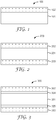
- FIG. 1 shows a cross sectional view of a multilayer structure 100 that in some implementations may be incorporated into a touch sensor.
- the structure 100 includes a coextruded core layer 101 and piezoelectric layer 102.
- the core layer is a non-piezoelectric polymer with the maximum magnitude piezoelectric strain coefficient in all orientations
- ⁇ 2 pC/N (where x 1,2,3).
- the piezoelectric layer 102 exhibits piezoelectric properties after it has been stretched and electrically poled to align the dipoles within the material. Alignment of the dipoles can be accomplished by heating the material and applying an electric field to the material while it is heated. Quenching the material after the heating and application of the electric field freezes the dipoles in alignment. Subsequent application of stress and/or deformation of the material creates a voltage across the material as the dipoles realign. Application of a voltage across the material causes the dipoles to realign which in turn causes deformation of the material
- the thickness of the multilayer structure 100 can be about 0.02 mm to 0.2 mm with the thickness of the piezoelectric layer being less than about 10 ⁇ m, less than about 7 ⁇ m, or less than about 5 ⁇ m, less than about 3 ⁇ m, less than about 2 ⁇ m, less than about 1 ⁇ m. In some embodiments the thickness of the piezoelectric layer is in a range of about 1 ⁇ m to about 5 ⁇ m.
- the core layer 101 is non-piezoelectric polymer having maximum magnitude piezolectric strain coefficient in all orientations
- ⁇ 2 pC/N (where x 1,2,3).
- the core layer may comprise a polymer selected to be compatible with the piezoelectric material to facilitate coextrusion and stretching of the multilayer structure.
- the piezoelectric material is polyvinylidene fluoride (PVDF)
- a suitable core layer may comprise poly(methyl) methacrylate (PMMA) or a blend of PMMA and modifiers such as Kraton, a synthetic block copolymer.
- the core layer may comprise a variety of materials including polypropylene (PP), polyvinyl chloride (PVC), polyethylene terephthalate (PET), Polyethylene naphthalate (PEN), or any other suitable material.
- Suitable core polymer materials should be optically clear, and include but are not limited to polyethylene naphthalate (PEN) and isomers thereof (such as 2,6-, 1,4-, 1,5-, 2,7-, and 2,3-PEN), polyalkylene terephthalates (such as polyethylene terephthalate, polybutylene terephthalate, and poly-1,4-cyclohexanedimethylene terephthalate), other polyesters, polycarbonates, polyarylates, polyamides (such as nylon 6, nylon 12, nylon 4/6, nylon 6/6, nylon 6/9, nylon 6/10, nylon 6/12, and nylon 6/T), polyimides (including thermoplastic polyimides and polyacrylic imides), polyamide-imides, polyether-amides, polyetherimides, polyaryl ethers (such as
- Copolymers of the present invention may be, for example, block copolymers, random copolymers, or alternating copolymers.
- Suitable comonomers for use in polyesters such as PET, PEN, PBN or the like may be of the diol or dicarboxylic acid or ester type.
- Dicarboxylic acid comonomers include but are not limited to terephthalic acid, isophthalic acid, phthalic acid, all isomeric naphthalenedicarboxylic acids (2,6-, 1,2-, 1,3-, 1,4-, 1,5-, 1,6-, 1,7-, 1,8-, 2,3-, 2,4-, 2,5-, 2,7-, and 2,8-), bibenzoic acids such as 4,4'-biphenyl dicarboxylic acid and its isomers, trans-4,4'-stilbene dicarboxylic acid and its isomers, 4,4'-diphenyl ether dicarboxylic acid and its isomers, 4,4'-diphenylsulfone dicarboxylic acid and its isomers, 4,4'-benzophenone dicarboxylic
- Suitable diol comonomers include but are not limited to linear or branched alkane diols or glycols (such as ethylene glycol, propanediols such as trimethylene glycol, butanediols such as tetramethylene glycol, pentanediols such as neopentyl glycol, hexanediols, 2,2,4-trimethyl-1,3-pentanediol and higher diols), ether glycols (such as diethylene glycol, triethylene glycol, and polyethylene glycol), chain-ester diols such as 3-hydroxy-2,2-dimethylpropyl-3-hydroxy-2,2-dimethyl propanoate, cycloalkane glycols such as 1,4-cyclohexanedimethanol and its isomers and 1,4-cyclohexanediol and its isomers, bi- or multicyclic diols (such as the various isomeric
- Tri- or polyfunctional comonomers which can serve to impart a branched structure to the polyester molecules, can also be used. They may be of either the carboxylic acid, ester, hydroxy or ether types. Examples include, but are not limited to, trimellitic acid and its esters, trimethylol propane, and pentaerythritol.
- comonomers are monomers of mixed functionality, including hydroxycarboxylic acids such as parahydroxybenzoic acid and 6-hydroxy-2-naphthalenecarboxylic acid, and their isomers, and tri- or polyfunctional comonomers of mixed functionality such as 5-hydroxyisophthalic acid and the like.
- the core layer 101 may be substantially optically transparent, flexible, and elastically deformable.
- the elastic modulus of the core material may be on the order of about 2.5 to 3 GPa, in other embodiments the elastic modulus of the core material may be on the order of 0.5 GPa. Or in a range between about 0.5 GPa and about 3 GPa.
- the core layer 101 can be designed to have specified resistivity and/or dielectric constant.
- the resistivity of the core layer 101 may be greater than about 10 15 ⁇ -cm or greater than about 10 17 Q-cm and the dielectric constant of the material can be less than 10, or less than 7, or less than 5, or in a range of about 2 to about 5.
- the core layer 101 can be relatively thick compared to the piezoelectric layer 102.
- the thickness of the core layer 101 may be more than 2 times, more than 5 times, or even more than 10 times the thickness of the piezoelectric layer 102.
- the piezoelectric layer 102 may be disposed directly on the core layer 101. In other implementations, there may be an intervening layer between the core layer 101 and the piezoelectric layer 102.
- the piezoelectric layer may be or comprise a layer of PVDF, a fluoropolymer, and/or copolymer of vinylidene fluoride and trifluoroethylene (TrFE).
- the piezoelectric layer is elastically deformable and in some implementations can have an elastic modulus in a range of about 1 to 1.5 GPa and may be substantially optically transparent.
- the PVDF of other layer is stretched to at least 4 times its original length (uniaxial stretching) or to at least 2 times its original length and width (biaxial stretching), and electrically poled. Stretching uniaxially by 5 times or more, or biaxially by 3 times or more can provide better properties.
- the piezoelectric layer may have crystallinity in a range of 40% to 60%, for example.
- the piezoelectric film may be poled simultaneously while being stretched or may be poled after the stretching.
- Poling PVDF can involve holding the film at a temperature of 80 to 120° C with exposure to an electric field of about 50 to 500 MV/m. The poling process may take 30 minutes to several hours which includes time for cooling. Alternatively, PVDF can be poled at room temperature using higher electrical fields, e.g., 100 to 800 MV/m. There are a number of methods that can be used to achieve the poling.
- the poled piezoelectric polymer has a piezoelectric voltage constant (d 33 ) of at least about 5 pC/N.
- the poled and stretched piezoelectric layer may have a resistivity greater than about 10 14 ⁇ -cm, for example, and a dielectric constant greater than that of the core, e.g., about 8 to 14.
- the relatively lower dielectric constant of the core material when compared to that of the piezoelectric layer may allow for higher electric field concentration in the piezoelectric layers of the multilayer structure when compared with a layer of similar thickness comprising the piezoelectric material without the core.
- the multilayer structure may additionally or alternatively have reduced leakage current due to the resistivity of the core, (on the order of 10 17 ⁇ -cm) which can be higher than the resistivity of the piezoelectric layer.
- the multilayer structure may also exhibit higher electrical breakdown strength than a similar thickness comprising the piezoelectric material without the core.
- the core may also have a higher elastic modulus than the piezoelectric layer.
- the core layer may have an elastic modulus higher, e.g., two or three times higher, than that of the piezoelectric layer.
- the core layer has an elastic modulus of about 3GPa and the piezoelectric layer has an elastic modulus about 1 to 1.5 GPa.
- the piezoelectric coefficients might be d 31 ⁇ 20 pC/N, d 32 ⁇ 2 pC/N, and d 33 ⁇ -30 pC/N.
- the directions are defined as is the convention with axis 1 being the direction in which the film is stretched, axis 2 being the orthogonal direction to axis 1 in the plan of the film and axis 3 being the direction normal to the plane of the film.
- d31 d32 (i.e., there is no difference in the plane of the film).
- the orientation of the crystals can be observed via techniques such as X-ray diffraction.
- FIG. 2 shows a cross sectional view of another multilayer structure 200 that includes a core layer 201 disposed between first and second piezoelectric layers 202, 203.
- the core and piezoelectric layers may be coextruded and have similar electrical, optical, and mechanical properties as described in connection with FIG. 1 .
- the core layer is a non-piezoelectric polymer with a maximum magnitude piezolectric strain coefficient in all orientations
- ⁇ 2 pC/N (where x 1,2,3).
- the overall thickness of the multilayer structure 200 may be about 0.025 mm to 0.15 mm.
- the core layer has a thickness at least about 1/6 the combined thickness of the core layer, the first piezoelectric layer 202 and the second piezoelectric layer 203. In some embodiments, the core layer has a thickness less than about 2/3 the combined thickness of the core layer, the first piezoelectric layer and the second piezoelectric layer.
- Each of the first and second piezoelectric layers may have a thickness less than about 10 ⁇ m, less than about 7 ⁇ m, or even less than about 5 ⁇ m, for example.
- a multilayer structure 300 may be coextruded including one or more tie layers 304, 305 disposed between at least one of the piezoelectric layers 302, 303 and the core layer 301.
- a tie layer between core layer 301 and one or both of the piezoelectric layers 302, 303 can allow use of a wider range of polymers for the core layer 301.
- a thin layer of PMMA could be used as a tie layer to increase the layer adhesion with a PP, PVC, PET, or PEN core layer.
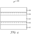
- the multilayer structure 400 may be coextruded to include a core layer 401 sandwiched between first and second piezoelectric layers 402, 403.
- skin layers 406, 407 can be disposed on the first and second piezoelectric layers 402, 403.
- the skin layers 406, 407 may be easily strippable, allowing them to be removed before further processing of the core 401 and piezoelectric layers 402, 403.
- the skin layers 406, 407 may be removed after stretching the multilayer structure 400.
- the skin layers 406, 407 may enhance the stretchability of the multilayer structure 400 and may also make it easier to handle.
- the skin layers 406, 407 can serve as temporary protective layers for the piezoelectric layers 402, 403, reducing damage to these layers during processing.
- skins made from PET will adhere well enough to piezoelectric layers of PVDF to allow for stretching and handling of the multilayer structure, but the PET skin layers can still be removed relatively easily for direct access to the PVDF layers, e.g., for fabrication of electrodes on the PVDF layers.
- the multilayer structures 100, 200, 300, 400 illustrated in FIGS. 1 through 4 are useful for touch sensing.
- Touch sensing involves determining information about a touch made to a touch surface, where the information may include detecting touch down, touch lift off, touch locations of one or multiple temporally overlapping touches, touch forces of one or multiple temporally overlapping touches, and/or other touch information.
- the time duration of the touches may range from a relatively short tap at a single location, to longer touches and/or touches that are tracked as the touches move across the touch surface.
- the piezoelectric layer When a touch is applied to the piezoelectric layer, dipoles in the piezoelectric layer are mechanically realigned, producing a transient voltage across the layer.
- the voltage signal can be detected using electrodes disposed on either side of the piezoelectric layer and analyzed to acquire touch information.
- the resolution of the touch location information is related to the distribution of individually addressable electrodes disposed across at least one side of a piezoelectric layer.
- FIG. 5 is a cross sectional view and FIG. 6 is a top view of touch sensor 500 that incorporates the multilayer structure 200 shown in FIG. 2 , but which could alternatively incorporate the multilayer structures 100, 300 shown in FIGS. 1 and 3 .
- the multilayer structure 200 includes a core layer 201 disposed between first and second piezoelectric layers 202, 203. Electrodes 502, 503 are disposed on either side of the multilayer structure 200. The electrodes can be deposited directly onto the piezoelectric layers.
- the electrodes may be transparent. Examples of transparent electrodes include indium tin oxide (ITO) and antimony doped tin oxide (ATO), silver nano-wires, and micro-wire meshes.
- the electrodes may be unpatterned, e.g., continuous, or patterned on one or both sides of the piezoelectric films.
- a patterned layer of a conductive material is formed on or over the first piezoelectric layer 202.
- the patterned layer provides a first set of individually addressable electrodes 502 that are electrically coupled to the first piezoelectric layer 202.
- An unpatterned layer of conductive material is formed on or over the second piezoelectric layer 203.
- the unpatterned layer provides a second electrode 503 that is electrically coupled to the second piezoelectric layer 203.
- Protective layers 504, 505 cover and protect the electrodes 502, 503.
- the surface 504a, 505a of either or both protective layers 504, 505 may form a touch surface of the touch sensor 500.
- One or both layers 504, 505 may be elastically deformable, allowing deformation of the piezoelectric layers 202, 203 in response to the touch.
- the first protective layer 504 is elastically deformable
- surface 504a forms the touch surface
- the second protective layer 505 is rigid.
- FIG. 7 is a cross sectional view of a touch sensor 700 that includes a patterned conductive layer disposed on or over both piezoelectric layers 202, 203 of the multilayer structure 200.
- the patterned conductive layers provide a first set of individually addressable electrodes 702 disposed on or over the first piezoelectric layer 202 and a second set of individually addressable electrodes 703 disposed over the second piezoelectric layer 203.
- the protective layers previously described in connection with FIGS. 5 and 6 are not shown in FIG. 7 .
- FIG. 8 is a cross sectional view illustrating a touch sensor 800 that is similar in some respects to the touch sensor 700 depicted in FIG. 7 .
- Touch sensor 800 additionally includes a first adhesion layer 802 disposed between the first set of electrodes 702 and the first piezoelectric layer 202 and a second adhesion layer 803 disposed between the second set of electrodes 703 and the second piezoelectric layer 203.
- the adhesion layers 802, 803 may be thin layers that are coextruded on the outer surfaces of the piezoelectric layers 202, 203.
- the adhesion layers 802, 803 enhance the bond between the electrodes 702, 703 and the piezoelectric layers 202, 203.
- a thin layer of PET could be used as an adhesion layer since many conductors are formulated to adhere to PET.
- the adhesion layers may be used in addition to tie layers (not shown) between the piezoelectric layers 202, 203 and the adhesion layers 802, 803 to enhance the bond strength between these layers.
- the tie layers are PMMA.
- the film surface may be treated chemically or via plasma, for example, to enhance the bond between the electrodes and the piezoelectric layers.
- FIG. 9 is a cross sectional view and FIG. 10 is a top view of a touch sensor 900 having a row and column electrode configuration.
- a first set of electrodes 902 are patterned as row electrodes disposed on or over the first piezoelectric layer 202 of multilayer structure 200.
- a second set of electrodes 903 are patterned as column electrodes disposed on or over the second piezoelectric layer 203 of multilayer structure 200.
- the row electrodes 902 can serve as sense electrodes and the column electrodes can serve as select electrodes 903, although the opposite configuration is also possible, wherein the row electrodes serve as select electrodes and the column electrodes serve as sense electrodes.
- FIG. 9 depicts first and second protective layers 904, 905 covering the electrodes 902, 903.
- select electrode 903a when select electrode 903a is selected, such as by electrically connecting the select electrode 903a to the sensing circuitry, sensing the electrical signal present at each row sense electrode 902 provides an indication of the deformation state of the piezoelectric layers 202, 203 at the location of each node 911 between the select electrode 903a and the sense electrodes 902.
- the select electrodes 903 are scanned, e.g., each select electrode is sequentially connected to the sense circuitry, and the voltages at the sense electrodes 902 is recorded to determine the deformation state at each node 911 across the touch surface.
- a voltage change at any of the nodes indicates a touch at the node location.
- the amount or degree of deformation can be used to determine the force of the touch on the touch surface.
- FIGS. 11 and 12 are cross sectional diagrams of the touch sensor 900 during touch down and touch lift off events, respectively.
- FIGS. 11 and 12 also show idealized versions of the signal output, V(t), of the touch sensor 900 during the touch down and touch lift off events.
- a touch applied to the touch surface by a touch implement causes a localized deformation of the touch surface 904a at the touch location 1110, which in turn causes a localized deformation of one or both of the piezoelectric layers 202, 203.
- the localized deformation of the piezoelectric layers produces a transient voltage signal 991 caused by movement of the dipoles in one or both of the piezoelectric layers 202, 203 during the deformation caused by the touch implement 999.
- the transient voltage signal 991 corresponding to a touch down event is detectable across the electrodes 902, 903 that are in the vicinity of the touch location 1110.
- Touch lift off occurs when the touch implement 999 is removed from the touch surface as illustrated in FIG. 12 .
- the touch surface elastically returns to its previous position.
- realignment of the dipoles in one or both of the piezoelectric layers produces a transient voltage signal 992 in the vicinity of the location 1110 of the previous touch.
- the transient voltage signal 992 corresponding to a touch lift off event is detectable between the electrodes 902, 903 that are in the vicinity of the touch location 1110.
- FIG. 13 shows a touch display system 1300 that includes circuitry for touch sensing, touch signal processing, and displaying information.
- a touch device includes a touch sensor 1301 and touch controller configured for touch sensing and touch signal processing.
- a display device includes a display and a display controller. The touch and display controllers may be coupled to a host computer. If the layers of the touch sensor 1301 are substantially optically transparent, the display may be arranged so that it is viewable through the touch sensor 1301.
- FIG. 13 depicts a touch sensor having row R1 - R5 and column C1 -C2 electrodes electrically coupled to touch controller circuitry.
- the touch controller includes electrode select circuitry, such as multiplexers, configured to scan through the select electrodes while sensing touch input signals from the sense electrodes using sensing circuitry.
- the sensing circuitry may include various signal processing components, such as filters, e.g., notch, bandpass, low and/or high pass filters, amplifiers, threshold detectors, analog-to-digital converters, and/or other signal processing components.
- the processed touch input signals are optionally analyzed by a touch information processor present in the touch controller.
- the touch information processor is configured to determine touch information based on the processed touch input signal.
- the processed touch input signals may be transferred to a host computer and the host computer determines the touch information.
- the multilayer structures depicted herein can be used to form touch sensors that can be used to determine touch information including touch location and touch force. While useful for touch sensing, the multilayer structures described and depicted herein may be implemented in a number of applications, including energy harvesting (harvesting the energy created by motion of the multilayer structure) and large area pressure sensing. In both large area pressure sensing and energy harvesting, multilayer structures similar to those depicted in FIGS. 1 through 8 may be used. In these applications, both of the electrode layers may be unpatterned as shown in FIGS. 14 and 15.
- FIG. 14 shows a device 1400 comprising multilayer structure 200 disposed between unpatterned electrode layers 1402, 1403. Protective layers 1404, 1405 are arranged on the electrode layers 1402, 1403.
- the multilayer structure 1400 can be used to form a piezoelectric cantilever that bends or moves, generating energy.
- the energy generated by movement of the multilayer structure 1400 can be stored in a capacitor or other energy storage device.
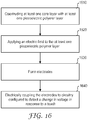
- FIG. 16 is a flow diagram illustrating a method of making multilayer structures discussed herein.
- the method includes coextruding 1610 at least one core layer with at least one piezoelectric polymer layer, forming a coextruded subsassembly.
- the coextruded subassembly is stretched, heated, and an electric field is applied 1620 to the heated subassembly to pole the piezoelectric polymer layer.
- Electrodes are formed 1630 on either side of the coextruded subassembly.
- the electrodes can optionally be coupled 1640 to circuitry configured to detect touch, pressure, or provide energy storage.
- the at least one piezoelectric polymer layer comprises a first piezoelectric polymer layer and a second piezoelectric polymer layer.
- coextruding the core layer with the at least one piezoelectric polymer layer comprises coextruding the core layer sandwiched between the first piezoelectric polymer layer and the second piezoelectric polymer layer.
- the coextruding can include coextruding a strippable layer disposed on the at least one piezoelectric polymer layer.
- the coextruding can include coextruding a first strippable layer on the first piezoelectric layer and a second strippable layer on the second piezoelectric layer. The strippable layers are stripped from the piezoelectric polymer layer and electrodes are formed on the piezoelectric layers.
- coextruding includes coextruding at least one of a first tie layer disposed between the core layer and a first piezoelectric polymer layer and a second tie layer disposed between the core layer and the second piezoelectric polymer layer.
- Coextruding may additionally or alternatively include one or more of coextruding a first adhesion layer on the first piezoelectric layer and coextruding a second adhesion layer on the second piezoelectric polymer layer.
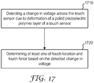
- FIG. 17 illustrates a method of using a multilayer structure described herein for touch sensing.
- the method include detecting 1710 a change in voltage across a electrodes of a touch sensor due to deformation of a poled piezoelectric layer of the touch sensor, the touch sensor including a core layer disposed between a first piezoelectric layer and a second piezoelectric layer, each piezoelectric layer comprising a poled piezoelectric polymer.
- the electrodes include at least a first electrode disposed over the first piezoelectric layer and at least a second electrode disposed over the second piezoelectric layer.
- One or both of the first and second electrodes comprise individually addressable electrodes.
- At least one of a touch location and touch force is determined 1720 based on the detected change in voltage.
- the at least one first electrode comprises a first set of individually addressable electrodes and the at least one second electrode comprises a second set of individually addressable electrodes.
- Detecting the change in voltage comprises detecting the change in voltage from an electrode of the first set referenced to an electrode of the second set.
- determining the touch location comprises determining locations of multiple touches that may occur simultaneously or substantially simultaneously.
- the touch locations of a touch that moves across the touch surface can be determined from the changes in voltages.
- Touch sensing using a piezoelectric-based sensor can facilitate detection of a gloved touch or a stylus touch, which is not as straightforwardly accomplished using other touch sensing methods such as capacitive sensing.
- a touch device may be configured incorporate both touch sensing techniques such that piezoelectric touch sensing is combined with capacitive touch sensing to enhance acquisition of touch sensing information.
- capacitive sensing can be used in certain circumstances, such as for finger touches, and piezoelectric touch sensing can be used in other circumstances, such as for stylus or gloved touches.
- piezoelectric sensing can be used to acquire some touch information, e.g., touch down, touch lift off and/or touch force
- capacitive touch sensing can be used to acquire different touch information, such as touch location.
- the piezoelectric sensing and capacitive sensing may use the same electrodes, with the touch controller circuitry including additional circuitry for driving electrodes for capacitive sensing.
- the touch controller circuitry may be configured to sequentially apply a drive signal to a first set of the electrodes and to sense the response signal at each electrode of a second set. Both the change in voltage across the touch sensor responsive to the deformation caused by the touch and the response signal indicative of a change in capacitance can be analyzed to provide information about the touch.
- the analysis may include separating the signal component generated by the piezoelectric layer from the signal component generated by the capacitive sensing.
- the signal component generated by the piezoelectric layer may be separated from the signal component generated by the capacitive sensing by appropriate filtering and/or other signal processing.
- a voltage applied across the multilayer structure including one or more piezoelectric layers can cause movement of the piezoelectric layers caused by alignment of the dipoles with the applied voltage. This phenomenon may be useful to provide haptic feedback to a user. For example, when a touch is detected at a location, a voltage may be applied to the electrodes at the touch location, causing movement of the piezoelectric layer that is discernible by the user.
Landscapes
- Engineering & Computer Science (AREA)
- General Engineering & Computer Science (AREA)
- Theoretical Computer Science (AREA)
- Physics & Mathematics (AREA)
- Manufacturing & Machinery (AREA)
- Human Computer Interaction (AREA)
- General Physics & Mathematics (AREA)
- Spectroscopy & Molecular Physics (AREA)
- Laminated Bodies (AREA)
- Position Input By Displaying (AREA)
Applications Claiming Priority (2)
| Application Number | Priority Date | Filing Date | Title |
|---|---|---|---|
| US201361907354P | 2013-11-21 | 2013-11-21 | |
| PCT/US2014/066055 WO2015077200A1 (en) | 2013-11-21 | 2014-11-18 | Multi-layer piezoelectric polymer film devices and methods |
Publications (3)
| Publication Number | Publication Date |
|---|---|
| EP3072169A1 EP3072169A1 (en) | 2016-09-28 |
| EP3072169A4 EP3072169A4 (en) | 2017-08-16 |
| EP3072169B1 true EP3072169B1 (en) | 2020-01-01 |
Family
ID=53180064
Family Applications (1)
| Application Number | Title | Priority Date | Filing Date |
|---|---|---|---|
| EP14864264.8A Active EP3072169B1 (en) | 2013-11-21 | 2014-11-18 | Multi-layer piezoelectric polymer film device |
Country Status (6)
Families Citing this family (64)
| Publication number | Priority date | Publication date | Assignee | Title |
|---|---|---|---|---|
| WO2015047572A1 (en) | 2013-09-24 | 2015-04-02 | 3M Innovative Properties Company | Transferable transparent conductive patterns and display stack materials |
| EP3108345B1 (en) | 2014-02-18 | 2019-12-25 | Cambridge Touch Technologies Limited | Dynamic switching of power modes for touch screens using force touch |
| US9690408B1 (en) | 2014-09-26 | 2017-06-27 | Apple Inc. | Electronic device with an integrated touch sensing and force sensing device |
| US9779676B2 (en) | 2014-09-30 | 2017-10-03 | Apple Inc. | Integrated touch sensor and force sensor for an electronic device |
| CN113655915B (zh) | 2014-12-23 | 2024-11-12 | 剑桥触控科技有限公司 | 压敏触摸面板 |
| GB2533667B (en) | 2014-12-23 | 2017-07-19 | Cambridge Touch Tech Ltd | Pressure-sensitive touch panel |
| US9939974B2 (en) * | 2014-12-29 | 2018-04-10 | Lg Display Co., Ltd. | Contact sensitive display device with thin profile and low external light reflectivity |
| US20160209961A1 (en) * | 2015-01-15 | 2016-07-21 | Electronics And Telecommunications Research Institute | Touch sensor |
| US10120449B2 (en) * | 2015-08-25 | 2018-11-06 | Immersion Corporation | Parallel plate actuator |
| US9891770B2 (en) | 2015-08-28 | 2018-02-13 | Apple Inc. | Methods for forming a patterned structure in a sensor |
| US10101857B2 (en) | 2015-08-28 | 2018-10-16 | Apple Inc. | Methods for integrating a compliant material with a substrate |
| US10635222B2 (en) * | 2015-10-02 | 2020-04-28 | Samsung Electronics Co., Ltd. | Touch pad and electronic apparatus using the same, and method of producing touch pad |
| KR102476610B1 (ko) | 2015-10-02 | 2022-12-12 | 삼성전자주식회사 | 터치 패드, 이를 이용한 터치 스크린 및 전자 장치, 및 터치 패드의 제조 방법 |
| KR102000992B1 (ko) * | 2015-10-05 | 2019-07-17 | 주식회사 아모그린텍 | 터치 압력 감지 장치 |
| JP6886460B2 (ja) * | 2015-10-13 | 2021-06-16 | コーニング インコーポレイテッド | 屈曲性電子装置モジュール、物品及びその製造方法 |
| GB2544307B (en) | 2015-11-12 | 2018-02-07 | Cambridge Touch Tech Ltd | Processing signals from a touchscreen panel |
| US10282046B2 (en) | 2015-12-23 | 2019-05-07 | Cambridge Touch Technologies Ltd. | Pressure-sensitive touch panel |
| GB2544353B (en) | 2015-12-23 | 2018-02-21 | Cambridge Touch Tech Ltd | Pressure-sensitive touch panel |
| KR102483412B1 (ko) * | 2015-12-31 | 2022-12-29 | 엘지디스플레이 주식회사 | 접촉 감응 소자 및 이를 포함하는 표시 장치 |
| GB2547031B (en) | 2016-02-05 | 2019-09-25 | Cambridge Touch Tech Ltd | Touchscreen panel signal processing |
| US10203793B2 (en) * | 2016-04-01 | 2019-02-12 | Microsoft Technology Licensing, Llc | Updating a display by applying pressure |
| US9965092B2 (en) | 2016-05-18 | 2018-05-08 | Apple Inc. | Managing power consumption of force sensors |
| KR102636735B1 (ko) * | 2016-09-20 | 2024-02-15 | 삼성디스플레이 주식회사 | 표시장치 |
| US10239212B2 (en) * | 2016-10-07 | 2019-03-26 | Southern Taiwan University Of Science And Technology | Ultrasonic tactile sensor for detecting clamping force |
| GB201617171D0 (en) | 2016-10-10 | 2016-11-23 | Universitetet I Troms� - Norges Arktiske Universitet | Piezoelectric films |
| KR102640240B1 (ko) * | 2016-10-31 | 2024-02-22 | 엘지디스플레이 주식회사 | 접촉 감응 소자 및 이를 포함하는 표시 장치 |
| KR102653711B1 (ko) | 2016-11-29 | 2024-04-01 | 엘지디스플레이 주식회사 | 접촉 감응 소자 및 그를 포함하는 표시 장치 |
| CN106648270B (zh) * | 2016-12-14 | 2017-11-28 | 西安交通大学 | 使用凝胶的柔性电容式多点触控触摸屏及制作方法 |
| US11063203B2 (en) * | 2017-01-08 | 2021-07-13 | Qualcomm Incorporated | Apparatus and method for poling a piezoelectric film |
| KR101885297B1 (ko) * | 2017-02-14 | 2018-08-03 | 중앙대학교 산학협력단 | 햅틱 피드백 버튼 |
| US11737366B2 (en) * | 2017-03-01 | 2023-08-22 | Rogers Corporation | Layered sensor apparatus and method of making same |
| KR102347989B1 (ko) * | 2017-04-14 | 2022-01-10 | 삼성디스플레이 주식회사 | 전자 장치 |
| US10353506B2 (en) | 2017-06-16 | 2019-07-16 | Apple Inc. | Dual resistive strain and pressure sensor for force touch |
| KR102353699B1 (ko) * | 2017-06-23 | 2022-01-19 | 엘지디스플레이 주식회사 | 터치 스크린 일체형 표시장치 |
| US11093088B2 (en) | 2017-08-08 | 2021-08-17 | Cambridge Touch Technologies Ltd. | Device for processing signals from a pressure-sensing touch panel |
| GB2565305A (en) | 2017-08-08 | 2019-02-13 | Cambridge Touch Tech Ltd | Device for processing signals from a pressure-sensing touch panel |
| KR101876438B1 (ko) * | 2017-08-10 | 2018-07-10 | 숭실대학교산학협력단 | 점유탄성 탄성중합체 기반 커패시터형 촉각센서 |
| US10585482B2 (en) | 2017-09-27 | 2020-03-10 | Apple Inc. | Electronic device having a hybrid conductive coating for electrostatic haptics |
| US10775890B2 (en) * | 2017-09-27 | 2020-09-15 | Apple Inc. | Electronic device having a piezoelectric body for friction haptics |
| US10248211B1 (en) | 2017-09-28 | 2019-04-02 | Apple Inc. | Ground-shifted touch input sensor for capacitively driving an electrostatic plate |
| US10871847B2 (en) | 2017-09-29 | 2020-12-22 | Apple Inc. | Sensing force and press location in absence of touch information |
| CN109901769B (zh) | 2017-12-07 | 2021-03-02 | 京东方科技集团股份有限公司 | 特征识别结构、制作方法、驱动方法及相关装置 |
| JP2019128315A (ja) * | 2018-01-26 | 2019-08-01 | シャープ株式会社 | 圧力検出装置及び表示装置 |
| JP2019169518A (ja) * | 2018-03-22 | 2019-10-03 | 株式会社東海理化電機製作所 | 圧電素子及び触覚呈示装置 |
| KR102164467B1 (ko) * | 2018-11-30 | 2020-10-13 | 피아이첨단소재 주식회사 | 입경이 상이한 2 이상의 필러를 포함하는 폴리이미드 필름 및 이를 포함하는 전자장치 |
| GB2581495A (en) | 2019-02-19 | 2020-08-26 | Cambridge Touch Tech Ltd | Force sensing touch panel |
| GB2582171B (en) | 2019-03-13 | 2022-10-12 | Cambridge Touch Tech Ltd | Force sensing touch panel |
| KR102811856B1 (ko) * | 2019-06-27 | 2025-05-22 | 엘지디스플레이 주식회사 | 센서 패널과 이를 포함하는 표시장치 |
| CN113821114B (zh) * | 2020-06-18 | 2024-12-10 | 宸鸿科技(厦门)有限公司 | 电子装置 |
| WO2022022831A1 (en) * | 2020-07-30 | 2022-02-03 | Uab Nanoenergija | Cantilever for a piezoelectric energy harvesting system |
| JP2022040711A (ja) * | 2020-08-31 | 2022-03-11 | 株式会社ジャパンディスプレイ | 圧力センサ |
| JP2022071284A (ja) * | 2020-10-28 | 2022-05-16 | シャープ株式会社 | タッチパネルシステム及び表示装置 |
| EP4238763A4 (en) * | 2020-10-30 | 2024-04-10 | Kureha Corporation | PIEZOELECTRIC FILM, TOUCH SCREEN AND MANUFACTURING METHOD OF PIEZOELECTRIC FILM |
| JP2022083296A (ja) | 2020-11-24 | 2022-06-03 | シャープ株式会社 | タッチパネルシステム、表示装置及びタッチパネルシステムの制御方法 |
| JP2022166512A (ja) | 2021-04-21 | 2022-11-02 | シャープディスプレイテクノロジー株式会社 | タッチパネルシステム及び表示装置 |
| CN115701319A (zh) * | 2021-05-28 | 2023-02-07 | 京东方科技集团股份有限公司 | 一种压电传感器、其制作方法及触觉反馈装置 |
| US12223110B1 (en) | 2021-09-23 | 2025-02-11 | Apple Inc. | Secure integrated circuit for smart haptics |
| FR3131088A1 (fr) * | 2021-12-17 | 2023-06-23 | Commissariat A L'energie Atomique Et Aux Energies Alternatives | Structure capacitive piezoelectrique |
| WO2023154249A1 (en) * | 2022-02-11 | 2023-08-17 | W. L. Gore & Associates, Inc. | Structurally reinforced ferroelectric articles of manufacture and methods of making and using the same |
| WO2023170729A1 (ja) * | 2022-03-07 | 2023-09-14 | 順治 曽根 | 皮膚刺激デバイスおよび皮膚刺激デバイスの駆動方法 |
| CN117321542A (zh) | 2022-04-27 | 2023-12-29 | 京东方科技集团股份有限公司 | 触控板 |
| JP2024115842A (ja) | 2023-02-15 | 2024-08-27 | シャープディスプレイテクノロジー株式会社 | タッチパネルシステム及び表示装置 |
| KR20250043069A (ko) | 2023-09-21 | 2025-03-28 | 전남대학교산학협력단 | 압전용 신축성 극한내성 셀룰로오스/pvdf 글리세로겔, 그 제조방법 및 이를 포함하는 응용제품 |
| WO2025094813A1 (ja) * | 2023-11-02 | 2025-05-08 | 株式会社村田製作所 | 変形検知センサ及び電子機器 |
Citations (1)
| Publication number | Priority date | Publication date | Assignee | Title |
|---|---|---|---|---|
| US20140082490A1 (en) * | 2012-09-18 | 2014-03-20 | Samsung Electronics Co., Ltd. | User terminal apparatus for providing local feedback and method thereof |
Family Cites Families (9)
| Publication number | Priority date | Publication date | Assignee | Title |
|---|---|---|---|---|
| JPS6125636U (ja) * | 1984-07-20 | 1986-02-15 | 日本ビクター株式会社 | 入力装置 |
| US6297579B1 (en) * | 2000-11-13 | 2001-10-02 | Sandia National Laboratories | Electron gun controlled smart structure |
| WO2009147741A1 (ja) * | 2008-06-05 | 2009-12-10 | 北陸電気工業株式会社 | タッチパネルを備えた表示装置及び圧電アクチュエータ |
| KR101516982B1 (ko) | 2008-12-24 | 2015-04-30 | 삼성전자주식회사 | 진동 터치 센서와 진동 터치 센싱 방법 및 진동 터치 스크린 디스플레이 패널 |
| KR101152554B1 (ko) | 2010-04-05 | 2012-06-01 | 삼성모바일디스플레이주식회사 | 터치 스크린 패널 및 이를 구비한 영상표시장치 |
| CN103069365B (zh) * | 2010-06-11 | 2017-01-18 | 3M创新有限公司 | 包括力测量的定位触摸传感器 |
| JP5597583B2 (ja) * | 2011-03-28 | 2014-10-01 | 太陽誘電株式会社 | タッチパネル装置及び電子機器 |
| CN102522494B (zh) * | 2011-12-14 | 2014-09-10 | 南京航空航天大学 | 同时具有驱动和传感能力的组合功能器件及其制备和应用 |
| US20130257744A1 (en) * | 2012-03-29 | 2013-10-03 | Intermec Technologies Corporation | Piezoelectric tactile interface |
-
2014
- 2014-11-18 US US15/034,969 patent/US9904428B2/en not_active Expired - Fee Related
- 2014-11-18 WO PCT/US2014/066055 patent/WO2015077200A1/en active Application Filing
- 2014-11-18 KR KR1020167015765A patent/KR20160088893A/ko not_active Withdrawn
- 2014-11-18 JP JP2016533068A patent/JP6420341B2/ja not_active Expired - Fee Related
- 2014-11-18 CN CN201480063643.9A patent/CN105765750B/zh not_active Expired - Fee Related
- 2014-11-18 EP EP14864264.8A patent/EP3072169B1/en active Active
Patent Citations (1)
| Publication number | Priority date | Publication date | Assignee | Title |
|---|---|---|---|---|
| US20140082490A1 (en) * | 2012-09-18 | 2014-03-20 | Samsung Electronics Co., Ltd. | User terminal apparatus for providing local feedback and method thereof |
Also Published As
| Publication number | Publication date |
|---|---|
| WO2015077200A1 (en) | 2015-05-28 |
| EP3072169A1 (en) | 2016-09-28 |
| KR20160088893A (ko) | 2016-07-26 |
| US9904428B2 (en) | 2018-02-27 |
| JP6420341B2 (ja) | 2018-11-07 |
| EP3072169A4 (en) | 2017-08-16 |
| CN105765750B (zh) | 2018-07-20 |
| CN105765750A (zh) | 2016-07-13 |
| US20160291729A1 (en) | 2016-10-06 |
| JP2017503241A (ja) | 2017-01-26 |
Similar Documents
| Publication | Publication Date | Title |
|---|---|---|
| EP3072169B1 (en) | Multi-layer piezoelectric polymer film device | |
| KR101993503B1 (ko) | 인쇄된 압전기 압력 감지 포일 | |
| JP6485618B2 (ja) | 圧電シートならびにそれを用いたタッチパネルならびにそれらを用いた入出力装置 | |
| EP2899615B1 (en) | Touch panel | |
| US20040263483A1 (en) | Sensing device | |
| KR102452755B1 (ko) | 투명 전극 형성 압전 필름 및 압력 센서 | |
| EP2323024A2 (en) | Multi-channel touch panel | |
| WO2013175848A1 (ja) | センサーデバイスおよび電子機器 | |
| CN104281328A (zh) | 一种触摸屏和显示面板 | |
| JP6879826B2 (ja) | タッチセンサ | |
| JP6103148B2 (ja) | 入力端末 | |
| KR20180099075A (ko) | 고성능 터치 센서 및 그 제조방법 | |
| KR20190013700A (ko) | 터치 센서 | |
| KR20190044625A (ko) | 터치 패널용 부재 | |
| EP3167261B1 (en) | Human-machine interface with graphene-pyroelectric materials | |
| WO2014168712A1 (en) | Touch panel, preparing method thereof, and ag-pd-nd alloy for touch panel | |
| TWI892597B (zh) | 輸入裝置及顯示裝置 | |
| CN106557211B (zh) | 一种三维触控总成 | |
| KR102532982B1 (ko) | 입력 센서 및 이를 포함하는 표시장치 | |
| JP2017058827A (ja) | タッチパネル及び電子機器 | |
| HK40024106A (en) | Flexible capacitive tactile sensor and preparation method thereof and tactile sensing system | |
| CN110998495A (zh) | 触摸屏 |
Legal Events
| Date | Code | Title | Description |
|---|---|---|---|
| PUAI | Public reference made under article 153(3) epc to a published international application that has entered the european phase |
Free format text: ORIGINAL CODE: 0009012 |
|
| 17P | Request for examination filed |
Effective date: 20160519 |
|
| AK | Designated contracting states |
Kind code of ref document: A1 Designated state(s): AL AT BE BG CH CY CZ DE DK EE ES FI FR GB GR HR HU IE IS IT LI LT LU LV MC MK MT NL NO PL PT RO RS SE SI SK SM TR |
|
| AX | Request for extension of the european patent |
Extension state: BA ME |
|
| DAX | Request for extension of the european patent (deleted) | ||
| REG | Reference to a national code |
Ref country code: DE Ref legal event code: R079 Ref document number: 602014059485 Country of ref document: DE Free format text: PREVIOUS MAIN CLASS: H01L0041253000 Ipc: G06F0003041000 |
|
| RIC1 | Information provided on ipc code assigned before grant |
Ipc: G06F 3/044 20060101ALI20170706BHEP Ipc: G06F 3/041 20060101AFI20170706BHEP Ipc: H01L 41/193 20060101ALI20170706BHEP |
|
| A4 | Supplementary search report drawn up and despatched |
Effective date: 20170714 |
|
| RIC1 | Information provided on ipc code assigned before grant |
Ipc: G06F 3/041 20060101AFI20170710BHEP Ipc: H01L 41/193 20060101ALI20170710BHEP Ipc: G06F 3/044 20060101ALI20170710BHEP |
|
| STAA | Information on the status of an ep patent application or granted ep patent |
Free format text: STATUS: EXAMINATION IS IN PROGRESS |
|
| 17Q | First examination report despatched |
Effective date: 20180329 |
|
| GRAP | Despatch of communication of intention to grant a patent |
Free format text: ORIGINAL CODE: EPIDOSNIGR1 |
|
| STAA | Information on the status of an ep patent application or granted ep patent |
Free format text: STATUS: GRANT OF PATENT IS INTENDED |
|
| INTG | Intention to grant announced |
Effective date: 20190730 |
|
| GRAS | Grant fee paid |
Free format text: ORIGINAL CODE: EPIDOSNIGR3 |
|
| GRAA | (expected) grant |
Free format text: ORIGINAL CODE: 0009210 |
|
| STAA | Information on the status of an ep patent application or granted ep patent |
Free format text: STATUS: THE PATENT HAS BEEN GRANTED |
|
| AK | Designated contracting states |
Kind code of ref document: B1 Designated state(s): AL AT BE BG CH CY CZ DE DK EE ES FI FR GB GR HR HU IE IS IT LI LT LU LV MC MK MT NL NO PL PT RO RS SE SI SK SM TR |
|
| REG | Reference to a national code |
Ref country code: GB Ref legal event code: FG4D |
|
| REG | Reference to a national code |
Ref country code: CH Ref legal event code: EP Ref country code: AT Ref legal event code: REF Ref document number: 1220613 Country of ref document: AT Kind code of ref document: T Effective date: 20200115 |
|
| REG | Reference to a national code |
Ref country code: DE Ref legal event code: R096 Ref document number: 602014059485 Country of ref document: DE |
|
| REG | Reference to a national code |
Ref country code: IE Ref legal event code: FG4D |
|
| REG | Reference to a national code |
Ref country code: NL Ref legal event code: MP Effective date: 20200101 |
|
| REG | Reference to a national code |
Ref country code: LT Ref legal event code: MG4D |
|
| PG25 | Lapsed in a contracting state [announced via postgrant information from national office to epo] |
Ref country code: RS Free format text: LAPSE BECAUSE OF FAILURE TO SUBMIT A TRANSLATION OF THE DESCRIPTION OR TO PAY THE FEE WITHIN THE PRESCRIBED TIME-LIMIT Effective date: 20200101 Ref country code: LT Free format text: LAPSE BECAUSE OF FAILURE TO SUBMIT A TRANSLATION OF THE DESCRIPTION OR TO PAY THE FEE WITHIN THE PRESCRIBED TIME-LIMIT Effective date: 20200101 Ref country code: NL Free format text: LAPSE BECAUSE OF FAILURE TO SUBMIT A TRANSLATION OF THE DESCRIPTION OR TO PAY THE FEE WITHIN THE PRESCRIBED TIME-LIMIT Effective date: 20200101 Ref country code: NO Free format text: LAPSE BECAUSE OF FAILURE TO SUBMIT A TRANSLATION OF THE DESCRIPTION OR TO PAY THE FEE WITHIN THE PRESCRIBED TIME-LIMIT Effective date: 20200401 Ref country code: PT Free format text: LAPSE BECAUSE OF FAILURE TO SUBMIT A TRANSLATION OF THE DESCRIPTION OR TO PAY THE FEE WITHIN THE PRESCRIBED TIME-LIMIT Effective date: 20200527 Ref country code: CZ Free format text: LAPSE BECAUSE OF FAILURE TO SUBMIT A TRANSLATION OF THE DESCRIPTION OR TO PAY THE FEE WITHIN THE PRESCRIBED TIME-LIMIT Effective date: 20200101 Ref country code: FI Free format text: LAPSE BECAUSE OF FAILURE TO SUBMIT A TRANSLATION OF THE DESCRIPTION OR TO PAY THE FEE WITHIN THE PRESCRIBED TIME-LIMIT Effective date: 20200101 |
|
| PG25 | Lapsed in a contracting state [announced via postgrant information from national office to epo] |
Ref country code: HR Free format text: LAPSE BECAUSE OF FAILURE TO SUBMIT A TRANSLATION OF THE DESCRIPTION OR TO PAY THE FEE WITHIN THE PRESCRIBED TIME-LIMIT Effective date: 20200101 Ref country code: LV Free format text: LAPSE BECAUSE OF FAILURE TO SUBMIT A TRANSLATION OF THE DESCRIPTION OR TO PAY THE FEE WITHIN THE PRESCRIBED TIME-LIMIT Effective date: 20200101 Ref country code: SE Free format text: LAPSE BECAUSE OF FAILURE TO SUBMIT A TRANSLATION OF THE DESCRIPTION OR TO PAY THE FEE WITHIN THE PRESCRIBED TIME-LIMIT Effective date: 20200101 Ref country code: GR Free format text: LAPSE BECAUSE OF FAILURE TO SUBMIT A TRANSLATION OF THE DESCRIPTION OR TO PAY THE FEE WITHIN THE PRESCRIBED TIME-LIMIT Effective date: 20200402 Ref country code: IS Free format text: LAPSE BECAUSE OF FAILURE TO SUBMIT A TRANSLATION OF THE DESCRIPTION OR TO PAY THE FEE WITHIN THE PRESCRIBED TIME-LIMIT Effective date: 20200501 Ref country code: BG Free format text: LAPSE BECAUSE OF FAILURE TO SUBMIT A TRANSLATION OF THE DESCRIPTION OR TO PAY THE FEE WITHIN THE PRESCRIBED TIME-LIMIT Effective date: 20200401 |
|
| REG | Reference to a national code |
Ref country code: DE Ref legal event code: R097 Ref document number: 602014059485 Country of ref document: DE |
|
| PG25 | Lapsed in a contracting state [announced via postgrant information from national office to epo] |
Ref country code: RO Free format text: LAPSE BECAUSE OF FAILURE TO SUBMIT A TRANSLATION OF THE DESCRIPTION OR TO PAY THE FEE WITHIN THE PRESCRIBED TIME-LIMIT Effective date: 20200101 Ref country code: ES Free format text: LAPSE BECAUSE OF FAILURE TO SUBMIT A TRANSLATION OF THE DESCRIPTION OR TO PAY THE FEE WITHIN THE PRESCRIBED TIME-LIMIT Effective date: 20200101 Ref country code: DK Free format text: LAPSE BECAUSE OF FAILURE TO SUBMIT A TRANSLATION OF THE DESCRIPTION OR TO PAY THE FEE WITHIN THE PRESCRIBED TIME-LIMIT Effective date: 20200101 Ref country code: EE Free format text: LAPSE BECAUSE OF FAILURE TO SUBMIT A TRANSLATION OF THE DESCRIPTION OR TO PAY THE FEE WITHIN THE PRESCRIBED TIME-LIMIT Effective date: 20200101 Ref country code: SM Free format text: LAPSE BECAUSE OF FAILURE TO SUBMIT A TRANSLATION OF THE DESCRIPTION OR TO PAY THE FEE WITHIN THE PRESCRIBED TIME-LIMIT Effective date: 20200101 Ref country code: SK Free format text: LAPSE BECAUSE OF FAILURE TO SUBMIT A TRANSLATION OF THE DESCRIPTION OR TO PAY THE FEE WITHIN THE PRESCRIBED TIME-LIMIT Effective date: 20200101 |
|
| PLBE | No opposition filed within time limit |
Free format text: ORIGINAL CODE: 0009261 |
|
| STAA | Information on the status of an ep patent application or granted ep patent |
Free format text: STATUS: NO OPPOSITION FILED WITHIN TIME LIMIT |
|
| REG | Reference to a national code |
Ref country code: AT Ref legal event code: MK05 Ref document number: 1220613 Country of ref document: AT Kind code of ref document: T Effective date: 20200101 |
|
| 26N | No opposition filed |
Effective date: 20201002 |
|
| PG25 | Lapsed in a contracting state [announced via postgrant information from national office to epo] |
Ref country code: AT Free format text: LAPSE BECAUSE OF FAILURE TO SUBMIT A TRANSLATION OF THE DESCRIPTION OR TO PAY THE FEE WITHIN THE PRESCRIBED TIME-LIMIT Effective date: 20200101 Ref country code: IT Free format text: LAPSE BECAUSE OF FAILURE TO SUBMIT A TRANSLATION OF THE DESCRIPTION OR TO PAY THE FEE WITHIN THE PRESCRIBED TIME-LIMIT Effective date: 20200101 |
|
| PGFP | Annual fee paid to national office [announced via postgrant information from national office to epo] |
Ref country code: DE Payment date: 20201103 Year of fee payment: 7 |
|
| PG25 | Lapsed in a contracting state [announced via postgrant information from national office to epo] |
Ref country code: PL Free format text: LAPSE BECAUSE OF FAILURE TO SUBMIT A TRANSLATION OF THE DESCRIPTION OR TO PAY THE FEE WITHIN THE PRESCRIBED TIME-LIMIT Effective date: 20200101 Ref country code: SI Free format text: LAPSE BECAUSE OF FAILURE TO SUBMIT A TRANSLATION OF THE DESCRIPTION OR TO PAY THE FEE WITHIN THE PRESCRIBED TIME-LIMIT Effective date: 20200101 |
|
| PG25 | Lapsed in a contracting state [announced via postgrant information from national office to epo] |
Ref country code: MC Free format text: LAPSE BECAUSE OF FAILURE TO SUBMIT A TRANSLATION OF THE DESCRIPTION OR TO PAY THE FEE WITHIN THE PRESCRIBED TIME-LIMIT Effective date: 20200101 |
|
| REG | Reference to a national code |
Ref country code: CH Ref legal event code: PL |
|
| GBPC | Gb: european patent ceased through non-payment of renewal fee |
Effective date: 20201118 |
|
| PG25 | Lapsed in a contracting state [announced via postgrant information from national office to epo] |
Ref country code: LU Free format text: LAPSE BECAUSE OF NON-PAYMENT OF DUE FEES Effective date: 20201118 |
|
| REG | Reference to a national code |
Ref country code: BE Ref legal event code: MM Effective date: 20201130 |
|
| PG25 | Lapsed in a contracting state [announced via postgrant information from national office to epo] |
Ref country code: LI Free format text: LAPSE BECAUSE OF NON-PAYMENT OF DUE FEES Effective date: 20201130 Ref country code: CH Free format text: LAPSE BECAUSE OF NON-PAYMENT OF DUE FEES Effective date: 20201130 |
|
| PG25 | Lapsed in a contracting state [announced via postgrant information from national office to epo] |
Ref country code: IE Free format text: LAPSE BECAUSE OF NON-PAYMENT OF DUE FEES Effective date: 20201118 Ref country code: FR Free format text: LAPSE BECAUSE OF NON-PAYMENT OF DUE FEES Effective date: 20201130 |
|
| PG25 | Lapsed in a contracting state [announced via postgrant information from national office to epo] |
Ref country code: GB Free format text: LAPSE BECAUSE OF NON-PAYMENT OF DUE FEES Effective date: 20201118 |
|
| PG25 | Lapsed in a contracting state [announced via postgrant information from national office to epo] |
Ref country code: TR Free format text: LAPSE BECAUSE OF FAILURE TO SUBMIT A TRANSLATION OF THE DESCRIPTION OR TO PAY THE FEE WITHIN THE PRESCRIBED TIME-LIMIT Effective date: 20200101 Ref country code: MT Free format text: LAPSE BECAUSE OF FAILURE TO SUBMIT A TRANSLATION OF THE DESCRIPTION OR TO PAY THE FEE WITHIN THE PRESCRIBED TIME-LIMIT Effective date: 20200101 Ref country code: CY Free format text: LAPSE BECAUSE OF FAILURE TO SUBMIT A TRANSLATION OF THE DESCRIPTION OR TO PAY THE FEE WITHIN THE PRESCRIBED TIME-LIMIT Effective date: 20200101 |
|
| REG | Reference to a national code |
Ref country code: DE Ref legal event code: R119 Ref document number: 602014059485 Country of ref document: DE |
|
| PG25 | Lapsed in a contracting state [announced via postgrant information from national office to epo] |
Ref country code: MK Free format text: LAPSE BECAUSE OF FAILURE TO SUBMIT A TRANSLATION OF THE DESCRIPTION OR TO PAY THE FEE WITHIN THE PRESCRIBED TIME-LIMIT Effective date: 20200101 Ref country code: AL Free format text: LAPSE BECAUSE OF FAILURE TO SUBMIT A TRANSLATION OF THE DESCRIPTION OR TO PAY THE FEE WITHIN THE PRESCRIBED TIME-LIMIT Effective date: 20200101 |
|
| PG25 | Lapsed in a contracting state [announced via postgrant information from national office to epo] |
Ref country code: BE Free format text: LAPSE BECAUSE OF NON-PAYMENT OF DUE FEES Effective date: 20201130 |
|
| PG25 | Lapsed in a contracting state [announced via postgrant information from national office to epo] |
Ref country code: DE Free format text: LAPSE BECAUSE OF NON-PAYMENT OF DUE FEES Effective date: 20220601 |