EP3072169B1 - Vorrichtung mit einem mehrschichtigen piezoelektrischen polymerfilm - Google Patents
Vorrichtung mit einem mehrschichtigen piezoelektrischen polymerfilm Download PDFInfo
- Publication number
- EP3072169B1 EP3072169B1 EP14864264.8A EP14864264A EP3072169B1 EP 3072169 B1 EP3072169 B1 EP 3072169B1 EP 14864264 A EP14864264 A EP 14864264A EP 3072169 B1 EP3072169 B1 EP 3072169B1
- Authority
- EP
- European Patent Office
- Prior art keywords
- layer
- piezoelectric
- touch
- electrodes
- touch panel
- Prior art date
- Legal status (The legal status is an assumption and is not a legal conclusion. Google has not performed a legal analysis and makes no representation as to the accuracy of the status listed.)
- Active
Links
Images


Classifications
-
- H—ELECTRICITY
- H10—SEMICONDUCTOR DEVICES; ELECTRIC SOLID-STATE DEVICES NOT OTHERWISE PROVIDED FOR
- H10N—ELECTRIC SOLID-STATE DEVICES NOT OTHERWISE PROVIDED FOR
- H10N30/00—Piezoelectric or electrostrictive devices
- H10N30/50—Piezoelectric or electrostrictive devices having a stacked or multilayer structure
-
- G—PHYSICS
- G06—COMPUTING; CALCULATING OR COUNTING
- G06F—ELECTRIC DIGITAL DATA PROCESSING
- G06F3/00—Input arrangements for transferring data to be processed into a form capable of being handled by the computer; Output arrangements for transferring data from processing unit to output unit, e.g. interface arrangements
- G06F3/01—Input arrangements or combined input and output arrangements for interaction between user and computer
- G06F3/03—Arrangements for converting the position or the displacement of a member into a coded form
- G06F3/041—Digitisers, e.g. for touch screens or touch pads, characterised by the transducing means
- G06F3/0414—Digitisers, e.g. for touch screens or touch pads, characterised by the transducing means using force sensing means to determine a position
- G06F3/04144—Digitisers, e.g. for touch screens or touch pads, characterised by the transducing means using force sensing means to determine a position using an array of force sensing means
-
- G—PHYSICS
- G06—COMPUTING; CALCULATING OR COUNTING
- G06F—ELECTRIC DIGITAL DATA PROCESSING
- G06F3/00—Input arrangements for transferring data to be processed into a form capable of being handled by the computer; Output arrangements for transferring data from processing unit to output unit, e.g. interface arrangements
- G06F3/01—Input arrangements or combined input and output arrangements for interaction between user and computer
- G06F3/016—Input arrangements with force or tactile feedback as computer generated output to the user
-
- G—PHYSICS
- G06—COMPUTING; CALCULATING OR COUNTING
- G06F—ELECTRIC DIGITAL DATA PROCESSING
- G06F3/00—Input arrangements for transferring data to be processed into a form capable of being handled by the computer; Output arrangements for transferring data from processing unit to output unit, e.g. interface arrangements
- G06F3/01—Input arrangements or combined input and output arrangements for interaction between user and computer
- G06F3/03—Arrangements for converting the position or the displacement of a member into a coded form
- G06F3/041—Digitisers, e.g. for touch screens or touch pads, characterised by the transducing means
- G06F3/0414—Digitisers, e.g. for touch screens or touch pads, characterised by the transducing means using force sensing means to determine a position
- G06F3/04146—Digitisers, e.g. for touch screens or touch pads, characterised by the transducing means using force sensing means to determine a position using pressure sensitive conductive elements delivering a boolean signal and located between crossing sensing lines, e.g. located between X and Y sensing line layers
-
- G—PHYSICS
- G06—COMPUTING; CALCULATING OR COUNTING
- G06F—ELECTRIC DIGITAL DATA PROCESSING
- G06F3/00—Input arrangements for transferring data to be processed into a form capable of being handled by the computer; Output arrangements for transferring data from processing unit to output unit, e.g. interface arrangements
- G06F3/01—Input arrangements or combined input and output arrangements for interaction between user and computer
- G06F3/03—Arrangements for converting the position or the displacement of a member into a coded form
- G06F3/041—Digitisers, e.g. for touch screens or touch pads, characterised by the transducing means
- G06F3/044—Digitisers, e.g. for touch screens or touch pads, characterised by the transducing means by capacitive means
- G06F3/0445—Digitisers, e.g. for touch screens or touch pads, characterised by the transducing means by capacitive means using two or more layers of sensing electrodes, e.g. using two layers of electrodes separated by a dielectric layer
-
- G—PHYSICS
- G06—COMPUTING; CALCULATING OR COUNTING
- G06F—ELECTRIC DIGITAL DATA PROCESSING
- G06F3/00—Input arrangements for transferring data to be processed into a form capable of being handled by the computer; Output arrangements for transferring data from processing unit to output unit, e.g. interface arrangements
- G06F3/01—Input arrangements or combined input and output arrangements for interaction between user and computer
- G06F3/03—Arrangements for converting the position or the displacement of a member into a coded form
- G06F3/041—Digitisers, e.g. for touch screens or touch pads, characterised by the transducing means
- G06F3/044—Digitisers, e.g. for touch screens or touch pads, characterised by the transducing means by capacitive means
- G06F3/0446—Digitisers, e.g. for touch screens or touch pads, characterised by the transducing means by capacitive means using a grid-like structure of electrodes in at least two directions, e.g. using row and column electrodes
-
- G—PHYSICS
- G06—COMPUTING; CALCULATING OR COUNTING
- G06F—ELECTRIC DIGITAL DATA PROCESSING
- G06F3/00—Input arrangements for transferring data to be processed into a form capable of being handled by the computer; Output arrangements for transferring data from processing unit to output unit, e.g. interface arrangements
- G06F3/01—Input arrangements or combined input and output arrangements for interaction between user and computer
- G06F3/03—Arrangements for converting the position or the displacement of a member into a coded form
- G06F3/041—Digitisers, e.g. for touch screens or touch pads, characterised by the transducing means
- G06F3/044—Digitisers, e.g. for touch screens or touch pads, characterised by the transducing means by capacitive means
- G06F3/0447—Position sensing using the local deformation of sensor cells
-
- H—ELECTRICITY
- H10—SEMICONDUCTOR DEVICES; ELECTRIC SOLID-STATE DEVICES NOT OTHERWISE PROVIDED FOR
- H10N—ELECTRIC SOLID-STATE DEVICES NOT OTHERWISE PROVIDED FOR
- H10N30/00—Piezoelectric or electrostrictive devices
- H10N30/01—Manufacture or treatment
-
- H—ELECTRICITY
- H10—SEMICONDUCTOR DEVICES; ELECTRIC SOLID-STATE DEVICES NOT OTHERWISE PROVIDED FOR
- H10N—ELECTRIC SOLID-STATE DEVICES NOT OTHERWISE PROVIDED FOR
- H10N30/00—Piezoelectric or electrostrictive devices
- H10N30/01—Manufacture or treatment
- H10N30/04—Treatments to modify a piezoelectric or electrostrictive property, e.g. polarisation characteristics, vibration characteristics or mode tuning
- H10N30/045—Treatments to modify a piezoelectric or electrostrictive property, e.g. polarisation characteristics, vibration characteristics or mode tuning by polarising
-
- H—ELECTRICITY
- H10—SEMICONDUCTOR DEVICES; ELECTRIC SOLID-STATE DEVICES NOT OTHERWISE PROVIDED FOR
- H10N—ELECTRIC SOLID-STATE DEVICES NOT OTHERWISE PROVIDED FOR
- H10N30/00—Piezoelectric or electrostrictive devices
- H10N30/01—Manufacture or treatment
- H10N30/05—Manufacture of multilayered piezoelectric or electrostrictive devices, or parts thereof, e.g. by stacking piezoelectric bodies and electrodes
- H10N30/057—Manufacture of multilayered piezoelectric or electrostrictive devices, or parts thereof, e.g. by stacking piezoelectric bodies and electrodes by stacking bulk piezoelectric or electrostrictive bodies and electrodes
-
- H—ELECTRICITY
- H10—SEMICONDUCTOR DEVICES; ELECTRIC SOLID-STATE DEVICES NOT OTHERWISE PROVIDED FOR
- H10N—ELECTRIC SOLID-STATE DEVICES NOT OTHERWISE PROVIDED FOR
- H10N30/00—Piezoelectric or electrostrictive devices
- H10N30/01—Manufacture or treatment
- H10N30/09—Forming piezoelectric or electrostrictive materials
- H10N30/098—Forming organic materials
-
- H—ELECTRICITY
- H10—SEMICONDUCTOR DEVICES; ELECTRIC SOLID-STATE DEVICES NOT OTHERWISE PROVIDED FOR
- H10N—ELECTRIC SOLID-STATE DEVICES NOT OTHERWISE PROVIDED FOR
- H10N30/00—Piezoelectric or electrostrictive devices
- H10N30/30—Piezoelectric or electrostrictive devices with mechanical input and electrical output, e.g. functioning as generators or sensors
-
- H—ELECTRICITY
- H10—SEMICONDUCTOR DEVICES; ELECTRIC SOLID-STATE DEVICES NOT OTHERWISE PROVIDED FOR
- H10N—ELECTRIC SOLID-STATE DEVICES NOT OTHERWISE PROVIDED FOR
- H10N30/00—Piezoelectric or electrostrictive devices
- H10N30/80—Constructional details
- H10N30/85—Piezoelectric or electrostrictive active materials
- H10N30/857—Macromolecular compositions
Claims (15)
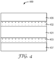
- Ein Touchpanel, umfassend:einen Berührungssensor (500, 700, 800, 900, 1301, 1400), umfassend:eine Berührungsoberfläche (504a, 505a, 904a, 1404a, 1405a);eine dielektrische Kernschicht (201, 301, 401);mindestens eine erste piezoelektrische Schicht (202, 302, 402) und eine zweite piezoelektrische Schicht (203, 303, 403), wobei die dielektrische Kernschicht zwischen der ersten und der zweiten piezoelektrischen Schicht angeordnet ist, wobei jede piezoelektrische Schicht ein gepoltes piezoelektrisches Polymer umfasst;mindestens einen ersten Satz einzeln ansteuerbarer Elektroden (502, 702, 902, 1402), die über der ersten piezoelektrischen Schicht angeordnet sind; undmindestens eine zweite Elektrode (503, 703, 903, 1403), die über der zweiten piezoelektrischen Schicht angeordnet ist; undeine Schaltung, die an den ersten Satz von Elektroden und die zweite Elektrode gekoppelt ist, wobei die Schaltung konfiguriert ist, eine Änderung eines elektrischen Signals von mindestens einer Elektrode des ersten Satzes von Elektroden, bezogen auf die zweite Elektrode als Reaktion auf eine Berührung, die an die Berührungsoberfläche angelegt wird, zu detektieren.
- Das Touchpanel nach Anspruch 1, wobei die mindestens eine zweite Elektrode einen zweiten Satz einzeln ansteuerbarer Elektroden umfasst und die Schaltung konfiguriert ist, um eine Änderung eines oder mehrerer elektrischer Signale von einer oder mehreren Elektroden des ersten Satzes, bezogen jeweils auf eine oder mehrere Elektroden des zweiten Satzes, zu detektieren.
- Das Touchpanel nach Anspruch 1, wobei die erste gepolte piezoelektrische Polymerschicht direkt auf einer ersten Oberfläche der Kernschicht angeordnet ist und die zweite gepolte piezoelektrische Polymerschicht direkt auf einer zweiten Oberfläche der Kernschicht angeordnet ist.
- Das Touchpanel nach Anspruch 1, wobei das gepolte piezoelektrische Polymer Polyvinylidenfluorid (PVDF) umfasst.
- Das Touchpanel nach Anspruch 1, wobei das gepolte piezoelektrische Polymer ein Fluorpolymer oder ein PVDF-Trifluorethylen-Copolymer (TrFE-Copolymer) umfasst.
- Das Touchpanel nach Anspruch 1, wobei das gepolte piezoelektrische Polymer eine piezoelektrische Spannungskonstante (d33) von mindestens etwa 5 pC/N aufweist.
- Das Touchpanel nach Anspruch 1, wobei die Kernschicht ein Polymer umfasst.
- Das Touchpanel nach Anspruch 1, wobei die Kernschicht Poly(methylmethacrylat (PMMA) umfasst.
- Das Touchpanel nach Anspruch 1, wobei die Kernschicht eine Dielektrizitätskonstante von etwa 2 bis etwa 5 aufweist.
- Das Touchpanel nach Anspruch 1, wobei die Kernschicht einen spezifischen Widerstand von mehr als etwa 1015 Ω-cm aufweist.
- Das Touchpanel nach Anspruch 1, wobei die Kernschicht einen Elastizitätsmodul in einem Bereich von etwa 0,5 GPa bis etwa 3 GPa aufweist.
- Das Touchpanel nach Anspruch 1, wobei die Kernschicht, die erste und die zweite piezoelektrische Schicht, der erste Satz von Elektroden und die mindestens eine zweite Elektrode im Wesentlichen optisch transparent sind.
- Das Touchpanel nach Anspruch 1, ferner umfassend eines oder mehrere von:einer ersten Verbindungsschicht, die zwischen der ersten piezoelektrischen Schicht und der Kernschicht angeordnet ist; undeiner zweiten Verbindungsschicht, die zwischen der zweiten piezoelektrischen Schicht und der Kernschicht angeordnet ist.
- Das Touchpanel nach Anspruch 1, ferner umfassend eines oder mehrere von:einer ersten Adhäsionsschicht, die zwischen dem ersten Satz von Elektroden und der ersten piezoelektrischen Schicht angeordnet ist; undeiner zweiten Adhäsionsschicht, die zwischen der mindestens einen zweiten Elektrode und der zweiten piezoelektrischen Schicht angeordnet ist.
- Das Touchpanel nach Anspruch 1, ferner umfassend mindestens eines von:einer ersten Schutzschicht, die über dem ersten Satz Elektroden angeordnet ist; undeiner zweiten Schutzschicht, die über der mindestens einen zweiten Elektrode angeordnet ist.
Applications Claiming Priority (2)
| Application Number | Priority Date | Filing Date | Title |
|---|---|---|---|
| US201361907354P | 2013-11-21 | 2013-11-21 | |
| PCT/US2014/066055 WO2015077200A1 (en) | 2013-11-21 | 2014-11-18 | Multi-layer piezoelectric polymer film devices and methods |
Publications (3)
| Publication Number | Publication Date |
|---|---|
| EP3072169A1 EP3072169A1 (de) | 2016-09-28 |
| EP3072169A4 EP3072169A4 (de) | 2017-08-16 |
| EP3072169B1 true EP3072169B1 (de) | 2020-01-01 |
Family
ID=53180064
Family Applications (1)
| Application Number | Title | Priority Date | Filing Date |
|---|---|---|---|
| EP14864264.8A Active EP3072169B1 (de) | 2013-11-21 | 2014-11-18 | Vorrichtung mit einem mehrschichtigen piezoelektrischen polymerfilm |
Country Status (6)
| Country | Link |
|---|---|
| US (1) | US9904428B2 (de) |
| EP (1) | EP3072169B1 (de) |
| JP (1) | JP6420341B2 (de) |
| KR (1) | KR20160088893A (de) |
| CN (1) | CN105765750B (de) |
| WO (1) | WO2015077200A1 (de) |
Families Citing this family (55)
| Publication number | Priority date | Publication date | Assignee | Title |
|---|---|---|---|---|
| CN105531114B (zh) | 2013-09-24 | 2017-10-10 | 3M创新有限公司 | 可转移的透明导电图案和显示器叠堆材料 |
| CN106030483B (zh) | 2014-02-18 | 2019-12-17 | 剑桥触控科技有限公司 | 使用压感触摸的触摸屏的功率模式的动态切换 |
| US9690408B1 (en) | 2014-09-26 | 2017-06-27 | Apple Inc. | Electronic device with an integrated touch sensing and force sensing device |
| US9779676B2 (en) | 2014-09-30 | 2017-10-03 | Apple Inc. | Integrated touch sensor and force sensor for an electronic device |
| GB2533667B (en) | 2014-12-23 | 2017-07-19 | Cambridge Touch Tech Ltd | Pressure-sensitive touch panel |
| KR102480003B1 (ko) | 2014-12-23 | 2022-12-21 | 케임브리지 터치 테크놀로지스 리미티드 | 압력감지 방식 터치 패널 |
| CN105761623B (zh) * | 2014-12-29 | 2019-03-08 | 乐金显示有限公司 | 显示装置 |
| US20160209961A1 (en) * | 2015-01-15 | 2016-07-21 | Electronics And Telecommunications Research Institute | Touch sensor |
| US10120449B2 (en) * | 2015-08-25 | 2018-11-06 | Immersion Corporation | Parallel plate actuator |
| US10101857B2 (en) | 2015-08-28 | 2018-10-16 | Apple Inc. | Methods for integrating a compliant material with a substrate |
| US9891770B2 (en) | 2015-08-28 | 2018-02-13 | Apple Inc. | Methods for forming a patterned structure in a sensor |
| KR102476610B1 (ko) * | 2015-10-02 | 2022-12-12 | 삼성전자주식회사 | 터치 패드, 이를 이용한 터치 스크린 및 전자 장치, 및 터치 패드의 제조 방법 |
| US10635222B2 (en) * | 2015-10-02 | 2020-04-28 | Samsung Electronics Co., Ltd. | Touch pad and electronic apparatus using the same, and method of producing touch pad |
| CN108369464B (zh) * | 2015-10-05 | 2021-11-05 | 阿莫绿色技术有限公司 | 触摸压力感测装置 |
| JP6886460B2 (ja) * | 2015-10-13 | 2021-06-16 | コーニング インコーポレイテッド | 屈曲性電子装置モジュール、物品及びその製造方法 |
| GB2544307B (en) | 2015-11-12 | 2018-02-07 | Cambridge Touch Tech Ltd | Processing signals from a touchscreen panel |
| GB2544353B (en) * | 2015-12-23 | 2018-02-21 | Cambridge Touch Tech Ltd | Pressure-sensitive touch panel |
| US10282046B2 (en) | 2015-12-23 | 2019-05-07 | Cambridge Touch Technologies Ltd. | Pressure-sensitive touch panel |
| KR102483412B1 (ko) * | 2015-12-31 | 2022-12-29 | 엘지디스플레이 주식회사 | 접촉 감응 소자 및 이를 포함하는 표시 장치 |
| GB2547031B (en) | 2016-02-05 | 2019-09-25 | Cambridge Touch Tech Ltd | Touchscreen panel signal processing |
| US10203793B2 (en) * | 2016-04-01 | 2019-02-12 | Microsoft Technology Licensing, Llc | Updating a display by applying pressure |
| US9965092B2 (en) | 2016-05-18 | 2018-05-08 | Apple Inc. | Managing power consumption of force sensors |
| KR102636735B1 (ko) * | 2016-09-20 | 2024-02-15 | 삼성디스플레이 주식회사 | 표시장치 |
| US10239212B2 (en) * | 2016-10-07 | 2019-03-26 | Southern Taiwan University Of Science And Technology | Ultrasonic tactile sensor for detecting clamping force |
| GB201617171D0 (en) | 2016-10-10 | 2016-11-23 | Universitetet I Troms� - Norges Arktiske Universitet | Piezoelectric films |
| KR102640240B1 (ko) * | 2016-10-31 | 2024-02-22 | 엘지디스플레이 주식회사 | 접촉 감응 소자 및 이를 포함하는 표시 장치 |
| KR102653711B1 (ko) * | 2016-11-29 | 2024-04-01 | 엘지디스플레이 주식회사 | 접촉 감응 소자 및 그를 포함하는 표시 장치 |
| CN106648270B (zh) * | 2016-12-14 | 2017-11-28 | 西安交通大学 | 使用凝胶的柔性电容式多点触控触摸屏及制作方法 |
| US11063203B2 (en) * | 2017-01-08 | 2021-07-13 | Qualcomm Incorporated | Apparatus and method for poling a piezoelectric film |
| KR101885297B1 (ko) * | 2017-02-14 | 2018-08-03 | 중앙대학교 산학협력단 | 햅틱 피드백 버튼 |
| US11737366B2 (en) * | 2017-03-01 | 2023-08-22 | Rogers Corporation | Layered sensor apparatus and method of making same |
| KR102347989B1 (ko) * | 2017-04-14 | 2022-01-10 | 삼성디스플레이 주식회사 | 전자 장치 |
| US10353506B2 (en) | 2017-06-16 | 2019-07-16 | Apple Inc. | Dual resistive strain and pressure sensor for force touch |
| KR102353699B1 (ko) * | 2017-06-23 | 2022-01-19 | 엘지디스플레이 주식회사 | 터치 스크린 일체형 표시장치 |
| US11093088B2 (en) | 2017-08-08 | 2021-08-17 | Cambridge Touch Technologies Ltd. | Device for processing signals from a pressure-sensing touch panel |
| GB2565305A (en) | 2017-08-08 | 2019-02-13 | Cambridge Touch Tech Ltd | Device for processing signals from a pressure-sensing touch panel |
| KR101876438B1 (ko) * | 2017-08-10 | 2018-07-10 | 숭실대학교산학협력단 | 점유탄성 탄성중합체 기반 커패시터형 촉각센서 |
| US10775890B2 (en) * | 2017-09-27 | 2020-09-15 | Apple Inc. | Electronic device having a piezoelectric body for friction haptics |
| US10585482B2 (en) | 2017-09-27 | 2020-03-10 | Apple Inc. | Electronic device having a hybrid conductive coating for electrostatic haptics |
| US10248211B1 (en) | 2017-09-28 | 2019-04-02 | Apple Inc. | Ground-shifted touch input sensor for capacitively driving an electrostatic plate |
| US10871847B2 (en) | 2017-09-29 | 2020-12-22 | Apple Inc. | Sensing force and press location in absence of touch information |
| CN109901769B (zh) * | 2017-12-07 | 2021-03-02 | 京东方科技集团股份有限公司 | 特征识别结构、制作方法、驱动方法及相关装置 |
| JP2019128315A (ja) * | 2018-01-26 | 2019-08-01 | シャープ株式会社 | 圧力検出装置及び表示装置 |
| JP2019169518A (ja) * | 2018-03-22 | 2019-10-03 | 株式会社東海理化電機製作所 | 圧電素子及び触覚呈示装置 |
| KR102164467B1 (ko) * | 2018-11-30 | 2020-10-13 | 피아이첨단소재 주식회사 | 입경이 상이한 2 이상의 필러를 포함하는 폴리이미드 필름 및 이를 포함하는 전자장치 |
| GB2581495A (en) | 2019-02-19 | 2020-08-26 | Cambridge Touch Tech Ltd | Force sensing touch panel |
| GB2582171B (en) | 2019-03-13 | 2022-10-12 | Cambridge Touch Tech Ltd | Force sensing touch panel |
| US20230070841A1 (en) * | 2020-07-30 | 2023-03-09 | Uab Nanoenergija | Cantilever For A Piezoelectric Energy Harvesting System |
| JP2022040711A (ja) * | 2020-08-31 | 2022-03-11 | 株式会社ジャパンディスプレイ | 圧力センサ |
| JP2022071284A (ja) * | 2020-10-28 | 2022-05-16 | シャープ株式会社 | タッチパネルシステム及び表示装置 |
| EP4238763A4 (de) * | 2020-10-30 | 2024-04-10 | Kureha Corp | Piezoelektrischer film, berührungsbildschirm und herstellungsverfahren für piezoelektrischen film |
| JP2022083296A (ja) | 2020-11-24 | 2022-06-03 | シャープ株式会社 | タッチパネルシステム、表示装置及びタッチパネルシステムの制御方法 |
| JP2022166512A (ja) | 2021-04-21 | 2022-11-02 | シャープディスプレイテクノロジー株式会社 | タッチパネルシステム及び表示装置 |
| CN115701319A (zh) * | 2021-05-28 | 2023-02-07 | 京东方科技集团股份有限公司 | 一种压电传感器、其制作方法及触觉反馈装置 |
| FR3131088A1 (fr) * | 2021-12-17 | 2023-06-23 | Commissariat A L'energie Atomique Et Aux Energies Alternatives | Structure capacitive piezoelectrique |
Citations (1)
| Publication number | Priority date | Publication date | Assignee | Title |
|---|---|---|---|---|
| US20140082490A1 (en) * | 2012-09-18 | 2014-03-20 | Samsung Electronics Co., Ltd. | User terminal apparatus for providing local feedback and method thereof |
Family Cites Families (9)
| Publication number | Priority date | Publication date | Assignee | Title |
|---|---|---|---|---|
| JPS6125636U (ja) * | 1984-07-20 | 1986-02-15 | 日本ビクター株式会社 | 入力装置 |
| US6297579B1 (en) * | 2000-11-13 | 2001-10-02 | Sandia National Laboratories | Electron gun controlled smart structure |
| US8773373B2 (en) | 2008-06-05 | 2014-07-08 | Hokuriku Electric Industry Co., Ltd. | Display apparatus with touch panel and piezoelectric actuator |
| KR101516982B1 (ko) * | 2008-12-24 | 2015-04-30 | 삼성전자주식회사 | 진동 터치 센서와 진동 터치 센싱 방법 및 진동 터치 스크린 디스플레이 패널 |
| KR101152554B1 (ko) * | 2010-04-05 | 2012-06-01 | 삼성모바일디스플레이주식회사 | 터치 스크린 패널 및 이를 구비한 영상표시장치 |
| SG186204A1 (en) * | 2010-06-11 | 2013-01-30 | 3M Innovative Properties Co | Positional touch sensor with force measurement |
| JP5597583B2 (ja) | 2011-03-28 | 2014-10-01 | 太陽誘電株式会社 | タッチパネル装置及び電子機器 |
| CN102522494B (zh) * | 2011-12-14 | 2014-09-10 | 南京航空航天大学 | 同时具有驱动和传感能力的组合功能器件及其制备和应用 |
| US20130257744A1 (en) * | 2012-03-29 | 2013-10-03 | Intermec Technologies Corporation | Piezoelectric tactile interface |
-
2014
- 2014-11-18 CN CN201480063643.9A patent/CN105765750B/zh not_active Expired - Fee Related
- 2014-11-18 US US15/034,969 patent/US9904428B2/en not_active Expired - Fee Related
- 2014-11-18 EP EP14864264.8A patent/EP3072169B1/de active Active
- 2014-11-18 WO PCT/US2014/066055 patent/WO2015077200A1/en active Application Filing
- 2014-11-18 JP JP2016533068A patent/JP6420341B2/ja not_active Expired - Fee Related
- 2014-11-18 KR KR1020167015765A patent/KR20160088893A/ko not_active Application Discontinuation
Patent Citations (1)
| Publication number | Priority date | Publication date | Assignee | Title |
|---|---|---|---|---|
| US20140082490A1 (en) * | 2012-09-18 | 2014-03-20 | Samsung Electronics Co., Ltd. | User terminal apparatus for providing local feedback and method thereof |
Also Published As
| Publication number | Publication date |
|---|---|
| US9904428B2 (en) | 2018-02-27 |
| EP3072169A4 (de) | 2017-08-16 |
| KR20160088893A (ko) | 2016-07-26 |
| US20160291729A1 (en) | 2016-10-06 |
| JP2017503241A (ja) | 2017-01-26 |
| JP6420341B2 (ja) | 2018-11-07 |
| CN105765750A (zh) | 2016-07-13 |
| EP3072169A1 (de) | 2016-09-28 |
| CN105765750B (zh) | 2018-07-20 |
| WO2015077200A1 (en) | 2015-05-28 |
Similar Documents
| Publication | Publication Date | Title |
|---|---|---|
| EP3072169B1 (de) | Vorrichtung mit einem mehrschichtigen piezoelektrischen polymerfilm | |
| JP6485618B2 (ja) | 圧電シートならびにそれを用いたタッチパネルならびにそれらを用いた入出力装置 | |
| EP2893423B1 (de) | Bedruckte piezoelektrische druckerfassungsfolie | |
| EP2899615B1 (de) | Berührungstafel | |
| KR101623809B1 (ko) | 압압 검출 기능이 있는 터치 패널 | |
| US20040263483A1 (en) | Sensing device | |
| CN111256571A (zh) | 柔性电容触觉传感器及其制备方法和触觉传感系统 | |
| CN108509096B (zh) | 高性能触摸传感器及其制造方法 | |
| KR102452755B1 (ko) | 투명 전극 형성 압전 필름 및 압력 센서 | |
| CN104281328A (zh) | 一种触摸屏和显示面板 | |
| WO2013175848A1 (ja) | センサーデバイスおよび電子機器 | |
| JP6103148B2 (ja) | 入力端末 | |
| KR102342378B1 (ko) | 터치 센서 | |
| JP6879826B2 (ja) | タッチセンサ | |
| KR102134319B1 (ko) | 터치 패널 및 그 제조 방법 | |
| KR20190044625A (ko) | 터치 패널용 부재 | |
| WO2014168712A1 (en) | Touch panel, preparing method thereof, and ag-pd-nd alloy for touch panel | |
| EP3167261B1 (de) | Mensch-maschine-schnittstelle mit graphen-pyroelektrischen materialien | |
| Firouzeh et al. | Poptouch: A submillimeter thick dynamically reconfigured haptic interface with pressable buttons | |
| CN106557211B (zh) | 一种三维触控总成 | |
| KR102532982B1 (ko) | 입력 센서 및 이를 포함하는 표시장치 | |
| JP2017058827A (ja) | タッチパネル及び電子機器 |
Legal Events
| Date | Code | Title | Description |
|---|---|---|---|
| PUAI | Public reference made under article 153(3) epc to a published international application that has entered the european phase |
Free format text: ORIGINAL CODE: 0009012 |
|
| 17P | Request for examination filed |
Effective date: 20160519 |
|
| AK | Designated contracting states |
Kind code of ref document: A1 Designated state(s): AL AT BE BG CH CY CZ DE DK EE ES FI FR GB GR HR HU IE IS IT LI LT LU LV MC MK MT NL NO PL PT RO RS SE SI SK SM TR |
|
| AX | Request for extension of the european patent |
Extension state: BA ME |
|
| DAX | Request for extension of the european patent (deleted) | ||
| REG | Reference to a national code |
Ref country code: DE Ref legal event code: R079 Ref document number: 602014059485 Country of ref document: DE Free format text: PREVIOUS MAIN CLASS: H01L0041253000 Ipc: G06F0003041000 |
|
| RIC1 | Information provided on ipc code assigned before grant |
Ipc: G06F 3/044 20060101ALI20170706BHEP Ipc: G06F 3/041 20060101AFI20170706BHEP Ipc: H01L 41/193 20060101ALI20170706BHEP |
|
| A4 | Supplementary search report drawn up and despatched |
Effective date: 20170714 |
|
| RIC1 | Information provided on ipc code assigned before grant |
Ipc: G06F 3/041 20060101AFI20170710BHEP Ipc: H01L 41/193 20060101ALI20170710BHEP Ipc: G06F 3/044 20060101ALI20170710BHEP |
|
| STAA | Information on the status of an ep patent application or granted ep patent |
Free format text: STATUS: EXAMINATION IS IN PROGRESS |
|
| 17Q | First examination report despatched |
Effective date: 20180329 |
|
| GRAP | Despatch of communication of intention to grant a patent |
Free format text: ORIGINAL CODE: EPIDOSNIGR1 |
|
| STAA | Information on the status of an ep patent application or granted ep patent |
Free format text: STATUS: GRANT OF PATENT IS INTENDED |
|
| INTG | Intention to grant announced |
Effective date: 20190730 |
|
| GRAS | Grant fee paid |
Free format text: ORIGINAL CODE: EPIDOSNIGR3 |
|
| GRAA | (expected) grant |
Free format text: ORIGINAL CODE: 0009210 |
|
| STAA | Information on the status of an ep patent application or granted ep patent |
Free format text: STATUS: THE PATENT HAS BEEN GRANTED |
|
| AK | Designated contracting states |
Kind code of ref document: B1 Designated state(s): AL AT BE BG CH CY CZ DE DK EE ES FI FR GB GR HR HU IE IS IT LI LT LU LV MC MK MT NL NO PL PT RO RS SE SI SK SM TR |
|
| REG | Reference to a national code |
Ref country code: GB Ref legal event code: FG4D |
|
| REG | Reference to a national code |
Ref country code: CH Ref legal event code: EP Ref country code: AT Ref legal event code: REF Ref document number: 1220613 Country of ref document: AT Kind code of ref document: T Effective date: 20200115 |
|
| REG | Reference to a national code |
Ref country code: DE Ref legal event code: R096 Ref document number: 602014059485 Country of ref document: DE |
|
| REG | Reference to a national code |
Ref country code: IE Ref legal event code: FG4D |
|
| REG | Reference to a national code |
Ref country code: NL Ref legal event code: MP Effective date: 20200101 |
|
| REG | Reference to a national code |
Ref country code: LT Ref legal event code: MG4D |
|
| PG25 | Lapsed in a contracting state [announced via postgrant information from national office to epo] |
Ref country code: RS Free format text: LAPSE BECAUSE OF FAILURE TO SUBMIT A TRANSLATION OF THE DESCRIPTION OR TO PAY THE FEE WITHIN THE PRESCRIBED TIME-LIMIT Effective date: 20200101 Ref country code: LT Free format text: LAPSE BECAUSE OF FAILURE TO SUBMIT A TRANSLATION OF THE DESCRIPTION OR TO PAY THE FEE WITHIN THE PRESCRIBED TIME-LIMIT Effective date: 20200101 Ref country code: NL Free format text: LAPSE BECAUSE OF FAILURE TO SUBMIT A TRANSLATION OF THE DESCRIPTION OR TO PAY THE FEE WITHIN THE PRESCRIBED TIME-LIMIT Effective date: 20200101 Ref country code: NO Free format text: LAPSE BECAUSE OF FAILURE TO SUBMIT A TRANSLATION OF THE DESCRIPTION OR TO PAY THE FEE WITHIN THE PRESCRIBED TIME-LIMIT Effective date: 20200401 Ref country code: PT Free format text: LAPSE BECAUSE OF FAILURE TO SUBMIT A TRANSLATION OF THE DESCRIPTION OR TO PAY THE FEE WITHIN THE PRESCRIBED TIME-LIMIT Effective date: 20200527 Ref country code: CZ Free format text: LAPSE BECAUSE OF FAILURE TO SUBMIT A TRANSLATION OF THE DESCRIPTION OR TO PAY THE FEE WITHIN THE PRESCRIBED TIME-LIMIT Effective date: 20200101 Ref country code: FI Free format text: LAPSE BECAUSE OF FAILURE TO SUBMIT A TRANSLATION OF THE DESCRIPTION OR TO PAY THE FEE WITHIN THE PRESCRIBED TIME-LIMIT Effective date: 20200101 |
|
| PG25 | Lapsed in a contracting state [announced via postgrant information from national office to epo] |
Ref country code: HR Free format text: LAPSE BECAUSE OF FAILURE TO SUBMIT A TRANSLATION OF THE DESCRIPTION OR TO PAY THE FEE WITHIN THE PRESCRIBED TIME-LIMIT Effective date: 20200101 Ref country code: LV Free format text: LAPSE BECAUSE OF FAILURE TO SUBMIT A TRANSLATION OF THE DESCRIPTION OR TO PAY THE FEE WITHIN THE PRESCRIBED TIME-LIMIT Effective date: 20200101 Ref country code: SE Free format text: LAPSE BECAUSE OF FAILURE TO SUBMIT A TRANSLATION OF THE DESCRIPTION OR TO PAY THE FEE WITHIN THE PRESCRIBED TIME-LIMIT Effective date: 20200101 Ref country code: GR Free format text: LAPSE BECAUSE OF FAILURE TO SUBMIT A TRANSLATION OF THE DESCRIPTION OR TO PAY THE FEE WITHIN THE PRESCRIBED TIME-LIMIT Effective date: 20200402 Ref country code: IS Free format text: LAPSE BECAUSE OF FAILURE TO SUBMIT A TRANSLATION OF THE DESCRIPTION OR TO PAY THE FEE WITHIN THE PRESCRIBED TIME-LIMIT Effective date: 20200501 Ref country code: BG Free format text: LAPSE BECAUSE OF FAILURE TO SUBMIT A TRANSLATION OF THE DESCRIPTION OR TO PAY THE FEE WITHIN THE PRESCRIBED TIME-LIMIT Effective date: 20200401 |
|
| REG | Reference to a national code |
Ref country code: DE Ref legal event code: R097 Ref document number: 602014059485 Country of ref document: DE |
|
| PG25 | Lapsed in a contracting state [announced via postgrant information from national office to epo] |
Ref country code: RO Free format text: LAPSE BECAUSE OF FAILURE TO SUBMIT A TRANSLATION OF THE DESCRIPTION OR TO PAY THE FEE WITHIN THE PRESCRIBED TIME-LIMIT Effective date: 20200101 Ref country code: ES Free format text: LAPSE BECAUSE OF FAILURE TO SUBMIT A TRANSLATION OF THE DESCRIPTION OR TO PAY THE FEE WITHIN THE PRESCRIBED TIME-LIMIT Effective date: 20200101 Ref country code: DK Free format text: LAPSE BECAUSE OF FAILURE TO SUBMIT A TRANSLATION OF THE DESCRIPTION OR TO PAY THE FEE WITHIN THE PRESCRIBED TIME-LIMIT Effective date: 20200101 Ref country code: EE Free format text: LAPSE BECAUSE OF FAILURE TO SUBMIT A TRANSLATION OF THE DESCRIPTION OR TO PAY THE FEE WITHIN THE PRESCRIBED TIME-LIMIT Effective date: 20200101 Ref country code: SM Free format text: LAPSE BECAUSE OF FAILURE TO SUBMIT A TRANSLATION OF THE DESCRIPTION OR TO PAY THE FEE WITHIN THE PRESCRIBED TIME-LIMIT Effective date: 20200101 Ref country code: SK Free format text: LAPSE BECAUSE OF FAILURE TO SUBMIT A TRANSLATION OF THE DESCRIPTION OR TO PAY THE FEE WITHIN THE PRESCRIBED TIME-LIMIT Effective date: 20200101 |
|
| PLBE | No opposition filed within time limit |
Free format text: ORIGINAL CODE: 0009261 |
|
| STAA | Information on the status of an ep patent application or granted ep patent |
Free format text: STATUS: NO OPPOSITION FILED WITHIN TIME LIMIT |
|
| REG | Reference to a national code |
Ref country code: AT Ref legal event code: MK05 Ref document number: 1220613 Country of ref document: AT Kind code of ref document: T Effective date: 20200101 |
|
| 26N | No opposition filed |
Effective date: 20201002 |
|
| PG25 | Lapsed in a contracting state [announced via postgrant information from national office to epo] |
Ref country code: AT Free format text: LAPSE BECAUSE OF FAILURE TO SUBMIT A TRANSLATION OF THE DESCRIPTION OR TO PAY THE FEE WITHIN THE PRESCRIBED TIME-LIMIT Effective date: 20200101 Ref country code: IT Free format text: LAPSE BECAUSE OF FAILURE TO SUBMIT A TRANSLATION OF THE DESCRIPTION OR TO PAY THE FEE WITHIN THE PRESCRIBED TIME-LIMIT Effective date: 20200101 |
|
| PGFP | Annual fee paid to national office [announced via postgrant information from national office to epo] |
Ref country code: DE Payment date: 20201103 Year of fee payment: 7 |
|
| PG25 | Lapsed in a contracting state [announced via postgrant information from national office to epo] |
Ref country code: PL Free format text: LAPSE BECAUSE OF FAILURE TO SUBMIT A TRANSLATION OF THE DESCRIPTION OR TO PAY THE FEE WITHIN THE PRESCRIBED TIME-LIMIT Effective date: 20200101 Ref country code: SI Free format text: LAPSE BECAUSE OF FAILURE TO SUBMIT A TRANSLATION OF THE DESCRIPTION OR TO PAY THE FEE WITHIN THE PRESCRIBED TIME-LIMIT Effective date: 20200101 |
|
| PG25 | Lapsed in a contracting state [announced via postgrant information from national office to epo] |
Ref country code: MC Free format text: LAPSE BECAUSE OF FAILURE TO SUBMIT A TRANSLATION OF THE DESCRIPTION OR TO PAY THE FEE WITHIN THE PRESCRIBED TIME-LIMIT Effective date: 20200101 |
|
| REG | Reference to a national code |
Ref country code: CH Ref legal event code: PL |
|
| GBPC | Gb: european patent ceased through non-payment of renewal fee |
Effective date: 20201118 |
|
| PG25 | Lapsed in a contracting state [announced via postgrant information from national office to epo] |
Ref country code: LU Free format text: LAPSE BECAUSE OF NON-PAYMENT OF DUE FEES Effective date: 20201118 |
|
| REG | Reference to a national code |
Ref country code: BE Ref legal event code: MM Effective date: 20201130 |
|
| PG25 | Lapsed in a contracting state [announced via postgrant information from national office to epo] |
Ref country code: LI Free format text: LAPSE BECAUSE OF NON-PAYMENT OF DUE FEES Effective date: 20201130 Ref country code: CH Free format text: LAPSE BECAUSE OF NON-PAYMENT OF DUE FEES Effective date: 20201130 |
|
| PG25 | Lapsed in a contracting state [announced via postgrant information from national office to epo] |
Ref country code: IE Free format text: LAPSE BECAUSE OF NON-PAYMENT OF DUE FEES Effective date: 20201118 Ref country code: FR Free format text: LAPSE BECAUSE OF NON-PAYMENT OF DUE FEES Effective date: 20201130 |
|
| PG25 | Lapsed in a contracting state [announced via postgrant information from national office to epo] |
Ref country code: GB Free format text: LAPSE BECAUSE OF NON-PAYMENT OF DUE FEES Effective date: 20201118 |
|
| PG25 | Lapsed in a contracting state [announced via postgrant information from national office to epo] |
Ref country code: TR Free format text: LAPSE BECAUSE OF FAILURE TO SUBMIT A TRANSLATION OF THE DESCRIPTION OR TO PAY THE FEE WITHIN THE PRESCRIBED TIME-LIMIT Effective date: 20200101 Ref country code: MT Free format text: LAPSE BECAUSE OF FAILURE TO SUBMIT A TRANSLATION OF THE DESCRIPTION OR TO PAY THE FEE WITHIN THE PRESCRIBED TIME-LIMIT Effective date: 20200101 Ref country code: CY Free format text: LAPSE BECAUSE OF FAILURE TO SUBMIT A TRANSLATION OF THE DESCRIPTION OR TO PAY THE FEE WITHIN THE PRESCRIBED TIME-LIMIT Effective date: 20200101 |
|
| REG | Reference to a national code |
Ref country code: DE Ref legal event code: R119 Ref document number: 602014059485 Country of ref document: DE |
|
| PG25 | Lapsed in a contracting state [announced via postgrant information from national office to epo] |
Ref country code: MK Free format text: LAPSE BECAUSE OF FAILURE TO SUBMIT A TRANSLATION OF THE DESCRIPTION OR TO PAY THE FEE WITHIN THE PRESCRIBED TIME-LIMIT Effective date: 20200101 Ref country code: AL Free format text: LAPSE BECAUSE OF FAILURE TO SUBMIT A TRANSLATION OF THE DESCRIPTION OR TO PAY THE FEE WITHIN THE PRESCRIBED TIME-LIMIT Effective date: 20200101 |
|
| PG25 | Lapsed in a contracting state [announced via postgrant information from national office to epo] |
Ref country code: BE Free format text: LAPSE BECAUSE OF NON-PAYMENT OF DUE FEES Effective date: 20201130 |
|
| PG25 | Lapsed in a contracting state [announced via postgrant information from national office to epo] |
Ref country code: DE Free format text: LAPSE BECAUSE OF NON-PAYMENT OF DUE FEES Effective date: 20220601 |