EP3072153B1 - Vorrichtung mit einem leistungselektronikmodul zum versorgen eines elektrischen verbrauchers eines haushaltsgeräts mit elektrischer versorgungsspannung, haushaltsgerät und verfahren zum herstellen einer derartigen vorrichtung - Google Patents
Vorrichtung mit einem leistungselektronikmodul zum versorgen eines elektrischen verbrauchers eines haushaltsgeräts mit elektrischer versorgungsspannung, haushaltsgerät und verfahren zum herstellen einer derartigen vorrichtung Download PDFInfo
- Publication number
- EP3072153B1 EP3072153B1 EP14796113.0A EP14796113A EP3072153B1 EP 3072153 B1 EP3072153 B1 EP 3072153B1 EP 14796113 A EP14796113 A EP 14796113A EP 3072153 B1 EP3072153 B1 EP 3072153B1
- Authority
- EP
- European Patent Office
- Prior art keywords
- circuit carrier
- power electronics
- electronics module
- temperature
- module
- Prior art date
- Legal status (The legal status is an assumption and is not a legal conclusion. Google has not performed a legal analysis and makes no representation as to the accuracy of the status listed.)
- Active
Links
Images


Classifications
-
- H—ELECTRICITY
- H10—SEMICONDUCTOR DEVICES; ELECTRIC SOLID-STATE DEVICES NOT OTHERWISE PROVIDED FOR
- H10W—GENERIC PACKAGES, INTERCONNECTIONS, CONNECTORS OR OTHER CONSTRUCTIONAL DETAILS OF DEVICES COVERED BY CLASS H10
- H10W40/00—Arrangements for thermal protection or thermal control
-
- H—ELECTRICITY
- H10—SEMICONDUCTOR DEVICES; ELECTRIC SOLID-STATE DEVICES NOT OTHERWISE PROVIDED FOR
- H10W—GENERIC PACKAGES, INTERCONNECTIONS, CONNECTORS OR OTHER CONSTRUCTIONAL DETAILS OF DEVICES COVERED BY CLASS H10
- H10W40/00—Arrangements for thermal protection or thermal control
- H10W40/20—Arrangements for cooling
- H10W40/25—Arrangements for cooling characterised by their materials
- H10W40/255—Arrangements for cooling characterised by their materials having a laminate or multilayered structure, e.g. direct bond copper [DBC] ceramic substrates
Definitions
- the invention relates to a device for supplying an electrical consumer of a household appliance with an electrical supply voltage, in particular with an AC voltage, comprising a power electronics module having a hybrid circuit board with a first circuit carrier and a second circuit carrier, wherein a transition region between the first and the second circuit carrier opposite the first and / or the second circuit carrier has lower thermal conductivity, and comprising a temperature protection device for temperature protection of the power electronics module.
- At least one semiconductor switch which is designed to generate the supply voltage for the electrical load, is arranged on the first circuit carrier of the hybrid printed circuit board.
- a temperature sensor of the temperature protection device is arranged, which is designed to detect a temperature to which the at least one semiconductor switch is exposed during operation of the device.
- the invention also relates to a household appliance with an electrical load, in particular an electric machine, and with a device according to the invention.
- the invention also relates to a method for producing such a device.
- Power electronics modules are used in household appliances for supplying electrical machines with alternating electrical voltage.
- Such power modules usually include a plurality of semiconductor switches, for example so-called IGBTs, which constitute a component of a so-called inverter and generate from a DC link voltage an electrical supply voltage with which an electrical machine or a drive motor is supplied.
- IGBTs semiconductor switches
- phases are generated, for example, three phases in a three-phase synchronous machine.
- the number of semiconductor switches used is then dependent the number of phases required.
- the transistors are connected here in a bridge circuit.
- a power module is for example from the document DE 10 2007 005 233 A1 known.
- the power semiconductors are sandwiched here between electrically insulating and highly heat-conductive layers, which are, for example, the ceramic cores of DCB / DAB or AMB substrates.
- This sandwich assembly is surrounded by a thin-walled shell of a metallic material and thermally connected via this to a heat sink.
- different shaped parts can be applied to this module shell, for example from embossed metal foil or the like.
- a cooling device for a power electronics module is for example from the document DE 10 2011 007 171 A1 known.
- the cooling device comprises a base body, on which at least partially a heat-dissipating graphite material is formed.
- the JP H04 273150 A deals with the problem of effectively dissipating the resulting heat loss from the power section of the circuit.
- a power unit is mounted on a different substrate, as the control part.
- One substrate is designed for a high thermal conductivity, while the other substrate is designed for an improved circuit. Both circuit parts are connected by means of bonding wires.
- the US 2009 0129432 A1 deals with the problem of thermally coupling a temperature protection circuit for a power circuit to the substrate of the power circuit.
- a terminal which leads from the power substrate to a piggy-backed circuit board, used as a heat conductor.
- a module is disclosed with a drive circuit for an electric power component of a transmission.
- the document is concerned with the protection of the circuit from the transmission fluid. Heat generated in the circuit is to be dissipated via the substrate to large-area copper conductor tracks on a printed circuit board.
- the US 5,747,875 deals with the dissipation of heat loss from a circuit unit with a power circuit part and a.
- the heat loss is thereby removed from the main circuit), which is applied to a power substrate, to a heat sink.
- a heat-conducting plate is provided, which is located on the underside of the housing and is in direct contact with the line substrate.
- the invention is based on a power electronics module in which a hybrid printed circuit board is used, which has two or more different circuit carriers, namely a first circuit carrier with at least one layer of a highly heat-conductive material - for example with at least one ceramic layer and optionally also with at least one metal layer - And a second circuit substrate having a significantly lower thermal conductivity - in particular of organic plastic, such as glass fiber reinforced epoxy resin (FR4).
- a hybrid circuit board can be made more cost-effective overall, since they do not have to be made entirely of ceramic.
- the power semiconductors are usually arranged on the ceramic circuit carrier, while other components, in particular serve the control of the semiconductor switches are mounted on the conventional FR4 circuit carrier. These components are, for example, so-called drivers for driving the semiconductor switches.
- a temperature sensor which serves to detect the temperature of the semiconductor switches is usually arranged on the conventional FR4 circuit carrier. This temperature sensor is part of a temperature protection device, which monitors the temperature of the semiconductor switches during operation and optionally interrupts the load circuit.
- the power electronics module is usually thermally connected to a heat sink with a relatively large contact pressure. Since the hybrid circuit board has only insufficient thermal conductivity, the heat is transferred here via the heat sink. However, if the heat sink is not mounted correctly, or if the contact pressure between the power module and the heat sink decreases, the temperature of the semiconductor switches will not be properly detected by the temperature sensor and over-temperature protection can no longer be ensured. In the worst case, this can lead to destruction of the entire electronic module.
- a device is designed to supply an electrical load, in particular an electrical machine, a household appliance with an electrical supply voltage, in particular with an AC voltage.
- the device comprises a power electronics module and a temperature protection device.
- the power electronics module has a hybrid circuit board with a first circuit carrier and a second circuit carrier. A transition region between the first and the second circuit carrier has a lower thermal conductivity than the first and / or the second circuit carrier.
- the second circuit carrier preferably has a lower thermal conductivity than the first circuit carrier.
- the temperature protection device is designed for temperature protection of the power electronics module.
- At least one semiconductor switch which is designed to generate the supply voltage for the electrical load, is arranged on the first circuit carrier of the hybrid printed circuit board.
- the at least one semiconductor switch can be, for example, an IGBT.
- a temperature sensor is arranged, which is designed to detect a temperature to which the at least one semiconductor switch is exposed during operation of the device.
- the temperature sensor thus detects the temperature of the at least one semiconductor switch.
- a thermally conductive foil is arranged on the power electronics module, in particular on a module housing, via which the at least one semiconductor switch and the temperature sensor are thermally coupled to one another.
- a heat-conducting foil is attached to the power electronics module.
- a thermally conductive film provides sufficient heat conduction or heat transfer between the semiconductor switch and the temperature sensor. This applies in particular even if this film is arranged between a heat sink and the power electronics module and the heat sink was incorrectly mounted or drops during operation of the device due to fatigue of a screw or a clamp connection. The heat transfer through the film is thus basically guaranteed even without the heat sink.
- the temperature of the semiconductor switch can be detected correctly during operation of the device and evaluated by a control unit accordingly. For example, if it is determined that the temperature exceeds a predetermined limit, the load circuit can be interrupted and the entire power electronics module can thus be reliably protected.
- the thermally conductive film extends at least substantially over the entire surface over at least one side of the power electronics module and thus overlaps both the temperature sensor and the at least one semiconductor switch.
- the film can be attached to a module housing of the power electronics module.
- the film is preferably located on a metallic housing region of the module housing, which contacts the first circuit carrier, and on a further housing region, which is made of plastic and contacts the second circuit carrier.
- the film rests on the temperature sensor and extends at least from the temperature sensor to the semiconductor switch and also rests on the semiconductor switch. The heat transfer then takes place preferably directly over the thermally conductive film.
- the first circuit carrier has at least one ceramic layer.
- the first circuit carrier may also have at least one metal layer.
- a circuit carrier made of ceramic proves to be particularly advantageous since ceramic has a relatively good thermal conductivity and thus ensures good heat distribution on the first circuit carrier and good heat coupling to the film.
- the second circuit carrier comprises organic plastic, preferably formed of organic plastic, in particular from a material comprising epoxy resin, such as glass fiber reinforced epoxy resin or FR4.
- organic plastics have a relatively low thermal conductivity, so that the film ensures reliable operation of the temperature protection device.
- the device additionally has a heat sink for heat dissipation from the power electronics module.
- the power electronics module is thermally connected via the film to the heat sink.
- the film is arranged in sandwich construction between the power electronics module on the one hand and the heat sink on the other.
- the film here assumes another function, namely the heat conduction from the power electronics module to the heat sink.
- the film is made of a material which comprises graphite and / or copper.
- a graphite foil or a copper foil can be used. It has been found that a 0.25 mm thick graphite foil is already sufficient to ensure good heat conduction between the semiconductor switch on the one hand and the temperature sensor. Experiments have shown that this is guaranteed even if the heat sink was mounted incorrectly and thus the required contact pressure was not given. Sufficient heat transfer is also given when the heat sink falls during operation, such as due to fatigue of the screw or clamp connection.
- the film is adhered to the power electronics module.
- a one-sided or two-sided self-adhesive heat-conducting foil can be used, which can be adhered to the power electronics module without much effort, without having to use additional adhesives.
- An adhesive bond also ensures a non-slip and thus reliable attachment and precise positioning of the film on the power electronics module.
- the invention also relates to a household appliance with an electrical load, in particular an electrical machine, and with a device according to the invention, which supplies the electrical load with electrical supply voltage.
- An inventive method is used to produce a device for supplying an electrical load of a household appliance with electrical supply voltage.
- a power electronics module is provided, which has a hybrid printed circuit board with a first circuit carrier and a second circuit carrier, which has a lower thermal conductivity, in particular with respect to the first circuit carrier. There is poor heat transfer between the first and second circuit carriers.
- a temperature protection device for temperature protection of the power electronics module is also provided, wherein at least one semiconductor switch, which is designed to generate the supply voltage, is arranged on the first circuit carrier, and on the second circuit carrier of the hybrid circuit board a temperature sensor of the temperature protection device is arranged for detecting a temperature of the semiconductor switch.
- a thermally conductive film is arranged, via which the at least one semiconductor switch and the temperature sensor are thermally connected to each other.
- the device 1 comprises a power electronics module 2 which comprises a hybrid printed circuit board 3 comprising a first circuit carrier 4 and a second circuit carrier 5.
- the first circuit carrier 4 has a greater thermal conductivity compared to the second circuit carrier 5.
- the first circuit carrier 4 is made of ceramic and may optionally also have a plurality of ceramic layers.
- the first circuit carrier 4 may optionally also have at least one metal layer.
- the second circuit carrier 5 is a conventional FR4 board in the embodiment.
- the circuit carriers 4, 5 are connected to one another in a transition region 19. Due to the design of the hybrid circuit board 3 of two separate circuit carriers 4, 5, the heat transfer in the transition region 19 is insufficient.
- the material of the second circuit substrate 5 also has insufficient thermal conductivity.
- the semiconductor switches 6 may be IGBTs.
- the semiconductor switches 6 are part of an inverter, which serves to generate an AC voltage as a supply voltage from a DC link voltage.
- a plurality of AC voltages can be generated when the electric machine is a multi-phase machine.
- a driver circuit 7 For driving the semiconductor switch 6, a driver circuit 7 is used, which is arranged on the second circuit carrier 5.
- a temperature sensor 8 for example, a negative temperature coefficient (NTC) sensor of a temperature protection device not specified is also arranged.
- NTC negative temperature coefficient
- further electronic components 9 can also be arranged on the second circuit carrier 5.
- the temperature sensor 8 is used to detect the temperature of the semiconductor switch 6 during operation of the device.
- the measured values of the temperature are transmitted to a control unit, which compares the measured values with a stored threshold value. If the threshold value is exceeded, the control unit can interrupt the load circuit of the semiconductor switch 6 and protect the device 1 or the power electronics module 2 from overheating.
- the power electronics module 2 has a module housing 14, in which the hybrid circuit board 3 is housed.
- the module housing 14 thus encloses or surrounds the hybrid printed circuit board 3 with the electronic components 6, 7, 8, 9.
- the module housing 14 is predominantly made of plastic. Only a rectangular housing portion 15 is made of metal, in particular of copper. This metallic housing region 15 bears directly against the first circuit carrier 4 and is arranged in mutual overlap with the semiconductor switches 6.
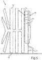
- Such a power electronics module 2, as it is in Fig. 1 is shown schematically, is mounted on a separate board 10, as in Fig. 5 shown.
- the board 10 is a conventional FR4 circuit board.
- the power electronics module 2 is electrically connected to the circuit board 10 via electrical contact elements 11.
- the connection is realized here in THT technology (Through Hole Technology).
- Said control unit and an electrical DC link with an intermediate circuit capacitor (not shown) are also arranged separately from the power electronics module 2 on the circuit board 10.
- Fig. 5 shows, in addition, a heat sink 12 for heat dissipation from the power electronics module 2 is mounted on the board 10.
- the power electronics module 2 is connected to the heat sink 12 with a relatively large contact force.
- the required contact pressure is usually realized by means of screw or clamp connection.
- a thermally conductive film 13 is glued to the power electronics module 2, for example, a self-adhesive film. This can be single-sided or double-sided adhesive.
- the film 13 is glued over its entire surface on a first side 16 of the power electronics module 2, on which also the metallic housing portion 15 is located.
- the film 13 thus thermally connects the housing region 15 with a further housing region 17 of the module housing 14, which is made of plastic and rests against the second circuit carrier 5.
- a thermal coupling is produced by the semiconductor switches 6, bypassing the transition region 19 via the good thermal conductivity of the first circuit substrate 4 and the metallic housing region 15 and furthermore via the film 13, the further housing region 17 and the second circuit carrier 5 to the temperature sensor 8.
- the film 13 extends over the entire surface of the first side 16 of the power electronics module 2 so that it is arranged in mutual overlap or overlapping at least both with the semiconductor switches 6 and with the temperature sensor 8.
- the power electronics module 2 is in a perspective view in Fig. 2 shown. Here, one of the first side 16 opposite second side 18 of the power electronics module 2 and the module housing 14 is shown. How out Fig. 2 shows, protrude from the module housing 14, the electrical contact elements 11, via which the power electronics module 2 is connected to the circuit board 10.
- Fig. 3 is a plan view of the first side 16 of the power electronics module 2 without the film 13 is shown.
- the metallic housing portion 15 is easily recognizable, which the first circuit carrier (see Fig. 1 ) overlaps.
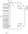
- Fig. 4 shows a plan view of the first side 16 of the power electronics module 2 including the film 13.
- the film 13 conceals both the metallic housing region 15 and the further housing region 17 and thus substantially the entire surface or the entire side 16 of the power electronics module 2.
- the film 13 is arranged in sandwich construction between the power electronics module 2 on the one hand and the heat sink 12 on the other.
- the film 13 here has two different functions: on the one hand the function of heat transfer between the semiconductor switches 6 and the temperature sensor 8 and on the other hand, the function of the heat conduction from the power electronics module 2 to the heat sink 12th
Landscapes
- Inverter Devices (AREA)
- Cooling Or The Like Of Semiconductors Or Solid State Devices (AREA)
- Cooling Or The Like Of Electrical Apparatus (AREA)
- Measuring Temperature Or Quantity Of Heat (AREA)
Priority Applications (1)
| Application Number | Priority Date | Filing Date | Title |
|---|---|---|---|
| PL14796113T PL3072153T3 (pl) | 2013-11-18 | 2014-11-11 | Urządzenie z modułem energoelektronicznym do zasilania elektrycznego odbiornika sprzętu gospodarstwa domowego elektrycznym napięciem zasilającym, sprzęt gospodarstwa domowego i sposób wytwarzania tego rodzaju urządzenia |
Applications Claiming Priority (2)
| Application Number | Priority Date | Filing Date | Title |
|---|---|---|---|
| DE102013223430.9A DE102013223430A1 (de) | 2013-11-18 | 2013-11-18 | Vorrichtung mit einem Leistungselektronikmodul zum Versorgen eines elektrischen Verbrauchers eines Haushaltsgeräts mit elektrischer Versorgungsspannung, Haushaltsgerät und Verfahren zum Herstellen einer derartigen Vorrichtung |
| PCT/EP2014/074226 WO2015071238A1 (de) | 2013-11-18 | 2014-11-11 | Vorrichtung mit einem leistungselektronikmodul zum versorgen eines elektrischen verbrauchers eines haushaltsgeräts mit elektrischer versorgungsspannung, haushaltsgerät und verfahren zum herstellen einer derartigen vorrichtung |
Publications (2)
| Publication Number | Publication Date |
|---|---|
| EP3072153A1 EP3072153A1 (de) | 2016-09-28 |
| EP3072153B1 true EP3072153B1 (de) | 2018-01-10 |
Family
ID=51871056
Family Applications (1)
| Application Number | Title | Priority Date | Filing Date |
|---|---|---|---|
| EP14796113.0A Active EP3072153B1 (de) | 2013-11-18 | 2014-11-11 | Vorrichtung mit einem leistungselektronikmodul zum versorgen eines elektrischen verbrauchers eines haushaltsgeräts mit elektrischer versorgungsspannung, haushaltsgerät und verfahren zum herstellen einer derartigen vorrichtung |
Country Status (7)
| Country | Link |
|---|---|
| EP (1) | EP3072153B1 (pl) |
| CN (1) | CN105745751B (pl) |
| DE (1) | DE102013223430A1 (pl) |
| ES (1) | ES2657703T3 (pl) |
| PL (1) | PL3072153T3 (pl) |
| RU (1) | RU2636415C1 (pl) |
| WO (1) | WO2015071238A1 (pl) |
Families Citing this family (4)
| Publication number | Priority date | Publication date | Assignee | Title |
|---|---|---|---|---|
| FR3082306B1 (fr) * | 2018-06-08 | 2020-09-18 | Valeo Equip Electr Moteur | Systeme de mesure d'une temperature d'un composant electrique et bras de commutation comportant un tel systeme |
| RU187623U1 (ru) * | 2018-10-24 | 2019-03-14 | Акционерное общество "Научно-исследовательский институт Приборостроения имени В.В. Тихомирова" | Радиоэлектронный узел |
| BE1027855B1 (de) * | 2019-12-13 | 2021-07-13 | Phoenix Contact Gmbh & Co | Verfahren zur Bestimmung eines Gehäuses für elektronische Bauteile |
| EP4318554A1 (de) * | 2022-08-02 | 2024-02-07 | Siemens Aktiengesellschaft | Halbleitermodul mit zumindest einer ersten halbleiteranordnung, einer zweiten halbleiteranordnung und einem kühlkörper |
Family Cites Families (22)
| Publication number | Priority date | Publication date | Assignee | Title |
|---|---|---|---|---|
| JPH04273150A (ja) * | 1991-02-28 | 1992-09-29 | Fuji Electric Co Ltd | 半導体装置 |
| DE4418426B4 (de) * | 1993-09-08 | 2007-08-02 | Mitsubishi Denki K.K. | Halbleiterleistungsmodul und Verfahren zur Herstellung des Halbleiterleistungsmoduls |
| JP2781329B2 (ja) * | 1992-10-21 | 1998-07-30 | 三菱電機株式会社 | 半導体パワーモジュールおよびその製造方法 |
| JPH07263621A (ja) * | 1994-03-18 | 1995-10-13 | Toshiba Corp | 半導体装置 |
| JP3206717B2 (ja) * | 1996-04-02 | 2001-09-10 | 富士電機株式会社 | 電力用半導体モジュール |
| JP2954908B2 (ja) * | 1997-09-30 | 1999-09-27 | エスエムシー株式会社 | 基板の温度調整装置 |
| JP3846699B2 (ja) * | 2001-10-10 | 2006-11-15 | 富士電機ホールディングス株式会社 | 半導体パワーモジュールおよびその製造方法 |
| DE10309302B4 (de) * | 2003-03-04 | 2007-09-27 | Semikron Elektronik Gmbh & Co. Kg | Leistungshalbleitermodul mit Sensorbauteil |
| JP2005109100A (ja) * | 2003-09-30 | 2005-04-21 | Mitsubishi Electric Corp | 半導体装置およびその製造方法 |
| DE102004019431A1 (de) * | 2004-04-19 | 2005-11-10 | Siemens Ag | Hybrider Leiterplattenaufbau zur kompakten Aufbautechnik von elektrischen Bauelementen |
| DE102004040773B3 (de) * | 2004-08-23 | 2005-05-25 | Siemens Ag | Halbleiterschaltgeräte mit Temeratursensor |
| DE102005013762C5 (de) * | 2005-03-22 | 2012-12-20 | Sew-Eurodrive Gmbh & Co. Kg | Elektronisches Gerät und Verfahren zur Bestimmung der Temperatur eines Leistungshalbleiters |
| DE102006056363B4 (de) * | 2006-11-29 | 2010-12-09 | Infineon Technologies Ag | Halbleitermodul mit mindestens zwei Substraten und Verfahren zur Herstellung eines Halbleitermoduls mit zwei Substraten |
| DE102007005233B4 (de) | 2007-01-30 | 2021-09-16 | Fraunhofer-Gesellschaft zur Förderung der angewandten Forschung e.V. | Leistungsmodul |
| DE102007052630B4 (de) * | 2007-11-05 | 2019-08-14 | Infineon Technologies Ag | Leistungshalbleitermodul mit Temperatursensor |
| US9064737B2 (en) * | 2007-11-13 | 2015-06-23 | Siemens Aktiengesellschaft | Power semiconductor module |
| US8057094B2 (en) * | 2007-11-16 | 2011-11-15 | Infineon Technologies Ag | Power semiconductor module with temperature measurement |
| JP4947135B2 (ja) * | 2009-12-04 | 2012-06-06 | 株式会社デンソー | 半導体パッケージおよびその製造方法 |
| DE102011007171A1 (de) | 2011-04-12 | 2012-10-18 | BSH Bosch und Siemens Hausgeräte GmbH | Kühlvorrichtung für ein Elektronikmodul eines Haushaltsgeräts sowie Baugruppe und Haushaltsgerät mit einer Kühlvorrichtung |
| DE102011080153A1 (de) * | 2011-07-29 | 2013-01-31 | Infineon Technologies Ag | Flexible verbindung von substraten in leistungshalbleitermodulen |
| DE102011088969A1 (de) * | 2011-12-19 | 2013-06-20 | Robert Bosch Gmbh | Getriebesteuermodul |
| RU124458U1 (ru) * | 2012-07-25 | 2013-01-20 | Открытое Акционерное Общество Научно-Производственное Объединение "Энергомодуль" (Оао Нпо "Энергомодуль") | Силовой модуль |
-
2013
- 2013-11-18 DE DE102013223430.9A patent/DE102013223430A1/de not_active Withdrawn
-
2014
- 2014-11-11 CN CN201480062736.XA patent/CN105745751B/zh active Active
- 2014-11-11 WO PCT/EP2014/074226 patent/WO2015071238A1/de not_active Ceased
- 2014-11-11 ES ES14796113.0T patent/ES2657703T3/es active Active
- 2014-11-11 EP EP14796113.0A patent/EP3072153B1/de active Active
- 2014-11-11 RU RU2016121113A patent/RU2636415C1/ru active
- 2014-11-11 PL PL14796113T patent/PL3072153T3/pl unknown
Also Published As
| Publication number | Publication date |
|---|---|
| PL3072153T3 (pl) | 2018-06-29 |
| CN105745751B (zh) | 2019-03-29 |
| ES2657703T3 (es) | 2018-03-06 |
| EP3072153A1 (de) | 2016-09-28 |
| CN105745751A (zh) | 2016-07-06 |
| RU2636415C1 (ru) | 2017-11-23 |
| DE102013223430A1 (de) | 2015-05-21 |
| WO2015071238A1 (de) | 2015-05-21 |
Similar Documents
| Publication | Publication Date | Title |
|---|---|---|
| DE102011104928B4 (de) | Kühlungsaufbau eines Kondensators und Umrichter damit | |
| DE102014212376B4 (de) | Halbleitervorrichtung | |
| DE112018005978T5 (de) | Halbleitervorrichtung | |
| DE112014002061T5 (de) | Halbleitermodul | |
| DE112015003987T5 (de) | Schaltungsbaugruppe, elektrischer Verteiler und Herstellungsverfahren für eine Schaltungsbaugruppe | |
| EP3072153B1 (de) | Vorrichtung mit einem leistungselektronikmodul zum versorgen eines elektrischen verbrauchers eines haushaltsgeräts mit elektrischer versorgungsspannung, haushaltsgerät und verfahren zum herstellen einer derartigen vorrichtung | |
| EP1062698A1 (de) | Elektronisches halbleitermodul | |
| DE102010006850A1 (de) | Elektronische Baugruppe zum Schalten elektrischer Leistung | |
| DE102007014713B3 (de) | Kühlanordnung, Umrichter und elektrisches Antriebssystem | |
| WO2014206665A1 (de) | Elektrische schaltung und verfahren zum herstellen einer elektrischen schaltung zur ansteuerung einer last | |
| WO2011066906A1 (de) | Leistungselektronische baugruppe und wechselrichteranordnung | |
| DE102014107703A1 (de) | Elektronische Vorrichtung | |
| DE102015219851B4 (de) | Steuergerät | |
| DE112018007231B4 (de) | Halbleiterbauelement und Leistungswandler | |
| DE102014109874A1 (de) | Elektronisches Element und elektronische Vorrichtung | |
| DE102019205772A1 (de) | Leistungsmodul mit gehäusten Leistungshalbleitern zur steuerbaren elektrischen Leistungsversorgung eines Verbrauchers | |
| WO2021105028A1 (de) | Leistungsmodul mit gehäusten leistungshalbleitern zur steuerbaren elektrischen leistungsversorgung eines verbrauchers sowie verfahren zur herstellung | |
| DE102020207708A1 (de) | Leistungsmodul zum Betreiben eines Elektrofahrzeugantriebs mit optimierter Erfassung der Chip-Temperatur | |
| DE202019106541U1 (de) | Leistungsmodul mit gehäusten Leistungshalbleitern zur steuerbaren elektrischen Leistungsversorgung eines Verbrauchers | |
| DE102019218157A1 (de) | Leistungsmodul mit gehäusten Leistungshalbleitern zur steuerbaren elektrischen Leistungsversorgung eines Verbrauchers sowie Verfahren zur Herstellung | |
| EP3648556B1 (en) | Power control modules | |
| DE102016218207A1 (de) | Elektronische Baugruppe, insbesondere eine elektronische Leistungsbaugruppe für Hybridfahrzeuge oder Elektrofahrzeuge | |
| DE102016209858B4 (de) | Elektronische Baugruppe, insbesondere für Elektrofahrzeuge oder Hybridfahrzeuge | |
| US20200020608A1 (en) | Circuit device | |
| DE102023202126A1 (de) | Inverter |
Legal Events
| Date | Code | Title | Description |
|---|---|---|---|
| PUAI | Public reference made under article 153(3) epc to a published international application that has entered the european phase |
Free format text: ORIGINAL CODE: 0009012 |
|
| 17P | Request for examination filed |
Effective date: 20160620 |
|
| AK | Designated contracting states |
Kind code of ref document: A1 Designated state(s): AL AT BE BG CH CY CZ DE DK EE ES FI FR GB GR HR HU IE IS IT LI LT LU LV MC MK MT NL NO PL PT RO RS SE SI SK SM TR |
|
| AX | Request for extension of the european patent |
Extension state: BA ME |
|
| DAX | Request for extension of the european patent (deleted) | ||
| GRAP | Despatch of communication of intention to grant a patent |
Free format text: ORIGINAL CODE: EPIDOSNIGR1 |
|
| INTG | Intention to grant announced |
Effective date: 20170713 |
|
| GRAS | Grant fee paid |
Free format text: ORIGINAL CODE: EPIDOSNIGR3 |
|
| GRAA | (expected) grant |
Free format text: ORIGINAL CODE: 0009210 |
|
| AK | Designated contracting states |
Kind code of ref document: B1 Designated state(s): AL AT BE BG CH CY CZ DE DK EE ES FI FR GB GR HR HU IE IS IT LI LT LU LV MC MK MT NL NO PL PT RO RS SE SI SK SM TR |
|
| REG | Reference to a national code |
Ref country code: CH Ref legal event code: EP Ref country code: AT Ref legal event code: REF Ref document number: 963289 Country of ref document: AT Kind code of ref document: T Effective date: 20180115 |
|
| REG | Reference to a national code |
Ref country code: IE Ref legal event code: FG4D Free format text: LANGUAGE OF EP DOCUMENT: GERMAN |
|
| REG | Reference to a national code |
Ref country code: DE Ref legal event code: R096 Ref document number: 502014006913 Country of ref document: DE |
|
| REG | Reference to a national code |
Ref country code: ES Ref legal event code: FG2A Ref document number: 2657703 Country of ref document: ES Kind code of ref document: T3 Effective date: 20180306 |
|
| REG | Reference to a national code |
Ref country code: NL Ref legal event code: MP Effective date: 20180110 |
|
| PG25 | Lapsed in a contracting state [announced via postgrant information from national office to epo] |
Ref country code: NL Free format text: LAPSE BECAUSE OF FAILURE TO SUBMIT A TRANSLATION OF THE DESCRIPTION OR TO PAY THE FEE WITHIN THE PRESCRIBED TIME-LIMIT Effective date: 20180110 |
|
| PG25 | Lapsed in a contracting state [announced via postgrant information from national office to epo] |
Ref country code: LT Free format text: LAPSE BECAUSE OF FAILURE TO SUBMIT A TRANSLATION OF THE DESCRIPTION OR TO PAY THE FEE WITHIN THE PRESCRIBED TIME-LIMIT Effective date: 20180110 Ref country code: CY Free format text: LAPSE BECAUSE OF FAILURE TO SUBMIT A TRANSLATION OF THE DESCRIPTION OR TO PAY THE FEE WITHIN THE PRESCRIBED TIME-LIMIT Effective date: 20180110 Ref country code: HR Free format text: LAPSE BECAUSE OF FAILURE TO SUBMIT A TRANSLATION OF THE DESCRIPTION OR TO PAY THE FEE WITHIN THE PRESCRIBED TIME-LIMIT Effective date: 20180110 Ref country code: FI Free format text: LAPSE BECAUSE OF FAILURE TO SUBMIT A TRANSLATION OF THE DESCRIPTION OR TO PAY THE FEE WITHIN THE PRESCRIBED TIME-LIMIT Effective date: 20180110 Ref country code: NO Free format text: LAPSE BECAUSE OF FAILURE TO SUBMIT A TRANSLATION OF THE DESCRIPTION OR TO PAY THE FEE WITHIN THE PRESCRIBED TIME-LIMIT Effective date: 20180410 |
|
| PG25 | Lapsed in a contracting state [announced via postgrant information from national office to epo] |
Ref country code: RS Free format text: LAPSE BECAUSE OF FAILURE TO SUBMIT A TRANSLATION OF THE DESCRIPTION OR TO PAY THE FEE WITHIN THE PRESCRIBED TIME-LIMIT Effective date: 20180110 Ref country code: GR Free format text: LAPSE BECAUSE OF FAILURE TO SUBMIT A TRANSLATION OF THE DESCRIPTION OR TO PAY THE FEE WITHIN THE PRESCRIBED TIME-LIMIT Effective date: 20180411 Ref country code: IS Free format text: LAPSE BECAUSE OF FAILURE TO SUBMIT A TRANSLATION OF THE DESCRIPTION OR TO PAY THE FEE WITHIN THE PRESCRIBED TIME-LIMIT Effective date: 20180510 Ref country code: SE Free format text: LAPSE BECAUSE OF FAILURE TO SUBMIT A TRANSLATION OF THE DESCRIPTION OR TO PAY THE FEE WITHIN THE PRESCRIBED TIME-LIMIT Effective date: 20180110 Ref country code: LV Free format text: LAPSE BECAUSE OF FAILURE TO SUBMIT A TRANSLATION OF THE DESCRIPTION OR TO PAY THE FEE WITHIN THE PRESCRIBED TIME-LIMIT Effective date: 20180110 Ref country code: BG Free format text: LAPSE BECAUSE OF FAILURE TO SUBMIT A TRANSLATION OF THE DESCRIPTION OR TO PAY THE FEE WITHIN THE PRESCRIBED TIME-LIMIT Effective date: 20180410 |
|
| PG25 | Lapsed in a contracting state [announced via postgrant information from national office to epo] |
Ref country code: MT Free format text: LAPSE BECAUSE OF FAILURE TO SUBMIT A TRANSLATION OF THE DESCRIPTION OR TO PAY THE FEE WITHIN THE PRESCRIBED TIME-LIMIT Effective date: 20180110 |
|
| REG | Reference to a national code |
Ref country code: DE Ref legal event code: R097 Ref document number: 502014006913 Country of ref document: DE |
|
| PG25 | Lapsed in a contracting state [announced via postgrant information from national office to epo] |
Ref country code: AL Free format text: LAPSE BECAUSE OF FAILURE TO SUBMIT A TRANSLATION OF THE DESCRIPTION OR TO PAY THE FEE WITHIN THE PRESCRIBED TIME-LIMIT Effective date: 20180110 Ref country code: EE Free format text: LAPSE BECAUSE OF FAILURE TO SUBMIT A TRANSLATION OF THE DESCRIPTION OR TO PAY THE FEE WITHIN THE PRESCRIBED TIME-LIMIT Effective date: 20180110 Ref country code: IT Free format text: LAPSE BECAUSE OF FAILURE TO SUBMIT A TRANSLATION OF THE DESCRIPTION OR TO PAY THE FEE WITHIN THE PRESCRIBED TIME-LIMIT Effective date: 20180110 Ref country code: RO Free format text: LAPSE BECAUSE OF FAILURE TO SUBMIT A TRANSLATION OF THE DESCRIPTION OR TO PAY THE FEE WITHIN THE PRESCRIBED TIME-LIMIT Effective date: 20180110 |
|
| PLBE | No opposition filed within time limit |
Free format text: ORIGINAL CODE: 0009261 |
|
| STAA | Information on the status of an ep patent application or granted ep patent |
Free format text: STATUS: NO OPPOSITION FILED WITHIN TIME LIMIT |
|
| PG25 | Lapsed in a contracting state [announced via postgrant information from national office to epo] |
Ref country code: SK Free format text: LAPSE BECAUSE OF FAILURE TO SUBMIT A TRANSLATION OF THE DESCRIPTION OR TO PAY THE FEE WITHIN THE PRESCRIBED TIME-LIMIT Effective date: 20180110 Ref country code: CZ Free format text: LAPSE BECAUSE OF FAILURE TO SUBMIT A TRANSLATION OF THE DESCRIPTION OR TO PAY THE FEE WITHIN THE PRESCRIBED TIME-LIMIT Effective date: 20180110 Ref country code: DK Free format text: LAPSE BECAUSE OF FAILURE TO SUBMIT A TRANSLATION OF THE DESCRIPTION OR TO PAY THE FEE WITHIN THE PRESCRIBED TIME-LIMIT Effective date: 20180110 Ref country code: SM Free format text: LAPSE BECAUSE OF FAILURE TO SUBMIT A TRANSLATION OF THE DESCRIPTION OR TO PAY THE FEE WITHIN THE PRESCRIBED TIME-LIMIT Effective date: 20180110 |
|
| 26N | No opposition filed |
Effective date: 20181011 |
|
| PG25 | Lapsed in a contracting state [announced via postgrant information from national office to epo] |
Ref country code: SI Free format text: LAPSE BECAUSE OF FAILURE TO SUBMIT A TRANSLATION OF THE DESCRIPTION OR TO PAY THE FEE WITHIN THE PRESCRIBED TIME-LIMIT Effective date: 20180110 |
|
| PGFP | Annual fee paid to national office [announced via postgrant information from national office to epo] |
Ref country code: ES Payment date: 20181218 Year of fee payment: 5 |
|
| REG | Reference to a national code |
Ref country code: CH Ref legal event code: PL |
|
| PG25 | Lapsed in a contracting state [announced via postgrant information from national office to epo] |
Ref country code: LU Free format text: LAPSE BECAUSE OF NON-PAYMENT OF DUE FEES Effective date: 20181111 Ref country code: MC Free format text: LAPSE BECAUSE OF FAILURE TO SUBMIT A TRANSLATION OF THE DESCRIPTION OR TO PAY THE FEE WITHIN THE PRESCRIBED TIME-LIMIT Effective date: 20180110 |
|
| REG | Reference to a national code |
Ref country code: BE Ref legal event code: MM Effective date: 20181130 |
|
| REG | Reference to a national code |
Ref country code: IE Ref legal event code: MM4A |
|
| PG25 | Lapsed in a contracting state [announced via postgrant information from national office to epo] |
Ref country code: LI Free format text: LAPSE BECAUSE OF NON-PAYMENT OF DUE FEES Effective date: 20181130 Ref country code: CH Free format text: LAPSE BECAUSE OF NON-PAYMENT OF DUE FEES Effective date: 20181130 |
|
| PG25 | Lapsed in a contracting state [announced via postgrant information from national office to epo] |
Ref country code: IE Free format text: LAPSE BECAUSE OF NON-PAYMENT OF DUE FEES Effective date: 20181111 Ref country code: FR Free format text: LAPSE BECAUSE OF NON-PAYMENT OF DUE FEES Effective date: 20181130 |
|
| PG25 | Lapsed in a contracting state [announced via postgrant information from national office to epo] |
Ref country code: BE Free format text: LAPSE BECAUSE OF NON-PAYMENT OF DUE FEES Effective date: 20181130 |
|
| PG25 | Lapsed in a contracting state [announced via postgrant information from national office to epo] |
Ref country code: PT Free format text: LAPSE BECAUSE OF FAILURE TO SUBMIT A TRANSLATION OF THE DESCRIPTION OR TO PAY THE FEE WITHIN THE PRESCRIBED TIME-LIMIT Effective date: 20180110 |
|
| PG25 | Lapsed in a contracting state [announced via postgrant information from national office to epo] |
Ref country code: MK Free format text: LAPSE BECAUSE OF NON-PAYMENT OF DUE FEES Effective date: 20180110 Ref country code: HU Free format text: LAPSE BECAUSE OF FAILURE TO SUBMIT A TRANSLATION OF THE DESCRIPTION OR TO PAY THE FEE WITHIN THE PRESCRIBED TIME-LIMIT; INVALID AB INITIO Effective date: 20141111 |
|
| GBPC | Gb: european patent ceased through non-payment of renewal fee |
Effective date: 20191111 |
|
| PG25 | Lapsed in a contracting state [announced via postgrant information from national office to epo] |
Ref country code: GB Free format text: LAPSE BECAUSE OF NON-PAYMENT OF DUE FEES Effective date: 20191111 |
|
| REG | Reference to a national code |
Ref country code: AT Ref legal event code: MM01 Ref document number: 963289 Country of ref document: AT Kind code of ref document: T Effective date: 20191111 |
|
| PG25 | Lapsed in a contracting state [announced via postgrant information from national office to epo] |
Ref country code: AT Free format text: LAPSE BECAUSE OF NON-PAYMENT OF DUE FEES Effective date: 20191111 |
|
| REG | Reference to a national code |
Ref country code: ES Ref legal event code: FD2A Effective date: 20210414 |
|
| PG25 | Lapsed in a contracting state [announced via postgrant information from national office to epo] |
Ref country code: ES Free format text: LAPSE BECAUSE OF NON-PAYMENT OF DUE FEES Effective date: 20191112 |
|
| PGFP | Annual fee paid to national office [announced via postgrant information from national office to epo] |
Ref country code: DE Payment date: 20241130 Year of fee payment: 11 |
|
| PGFP | Annual fee paid to national office [announced via postgrant information from national office to epo] |
Ref country code: PL Payment date: 20241029 Year of fee payment: 11 |
|
| PGFP | Annual fee paid to national office [announced via postgrant information from national office to epo] |
Ref country code: TR Payment date: 20241101 Year of fee payment: 11 |
|
| REG | Reference to a national code |
Ref country code: DE Ref legal event code: R079 Ref document number: 502014006913 Country of ref document: DE Free format text: PREVIOUS MAIN CLASS: H01L0023340000 Ipc: H10W0040000000 |