EP3014663B1 - Method and device for producing a photovoltaic element with stabilized efficiency - Google Patents
Method and device for producing a photovoltaic element with stabilized efficiency Download PDFInfo
- Publication number
- EP3014663B1 EP3014663B1 EP13770893.9A EP13770893A EP3014663B1 EP 3014663 B1 EP3014663 B1 EP 3014663B1 EP 13770893 A EP13770893 A EP 13770893A EP 3014663 B1 EP3014663 B1 EP 3014663B1
- Authority
- EP
- European Patent Office
- Prior art keywords
- hydrogen
- silicon substrate
- temperature
- silicon
- cooling
- Prior art date
- Legal status (The legal status is an assumption and is not a legal conclusion. Google has not performed a legal analysis and makes no representation as to the accuracy of the status listed.)
- Active
Links
- 238000000034 method Methods 0.000 title claims description 97
- 239000000758 substrate Substances 0.000 claims description 178
- 229910052710 silicon Inorganic materials 0.000 claims description 156
- 239000010703 silicon Substances 0.000 claims description 156
- XUIMIQQOPSSXEZ-UHFFFAOYSA-N Silicon Chemical compound [Si] XUIMIQQOPSSXEZ-UHFFFAOYSA-N 0.000 claims description 155
- 239000001257 hydrogen Substances 0.000 claims description 147
- 229910052739 hydrogen Inorganic materials 0.000 claims description 147
- UFHFLCQGNIYNRP-UHFFFAOYSA-N Hydrogen Chemical compound [H][H] UFHFLCQGNIYNRP-UHFFFAOYSA-N 0.000 claims description 142
- 239000002800 charge carrier Substances 0.000 claims description 47
- 238000001816 cooling Methods 0.000 claims description 46
- 238000004519 manufacturing process Methods 0.000 claims description 30
- 230000006641 stabilisation Effects 0.000 claims description 23
- HQVNEWCFYHHQES-UHFFFAOYSA-N silicon nitride Chemical group N12[Si]34N5[Si]62N3[Si]51N64 HQVNEWCFYHHQES-UHFFFAOYSA-N 0.000 claims description 15
- 238000005286 illumination Methods 0.000 claims description 10
- 238000010438 heat treatment Methods 0.000 claims description 8
- 238000007664 blowing Methods 0.000 claims description 3
- 238000000151 deposition Methods 0.000 claims description 3
- 239000000112 cooling gas Substances 0.000 claims description 2
- 238000012423 maintenance Methods 0.000 claims 3
- 230000003019 stabilising effect Effects 0.000 claims 1
- 230000008929 regeneration Effects 0.000 description 56
- 238000011069 regeneration method Methods 0.000 description 56
- 230000008569 process Effects 0.000 description 39
- 230000007547 defect Effects 0.000 description 31
- 239000000463 material Substances 0.000 description 22
- 239000013078 crystal Substances 0.000 description 21
- 239000001301 oxygen Substances 0.000 description 21
- 229910052760 oxygen Inorganic materials 0.000 description 21
- 238000011105 stabilization Methods 0.000 description 21
- QVGXLLKOCUKJST-UHFFFAOYSA-N atomic oxygen Chemical compound [O] QVGXLLKOCUKJST-UHFFFAOYSA-N 0.000 description 20
- 230000015556 catabolic process Effects 0.000 description 19
- 238000006731 degradation reaction Methods 0.000 description 19
- 230000000694 effects Effects 0.000 description 18
- ZOXJGFHDIHLPTG-UHFFFAOYSA-N Boron Chemical compound [B] ZOXJGFHDIHLPTG-UHFFFAOYSA-N 0.000 description 17
- 238000009792 diffusion process Methods 0.000 description 17
- 235000012431 wafers Nutrition 0.000 description 17
- 229910052796 boron Inorganic materials 0.000 description 16
- 150000002431 hydrogen Chemical class 0.000 description 11
- 239000004065 semiconductor Substances 0.000 description 11
- XGCTUKUCGUNZDN-UHFFFAOYSA-N [B].O=O Chemical compound [B].O=O XGCTUKUCGUNZDN-UHFFFAOYSA-N 0.000 description 10
- 230000002596 correlated effect Effects 0.000 description 9
- 229910052581 Si3N4 Inorganic materials 0.000 description 8
- 238000013459 approach Methods 0.000 description 8
- 238000002347 injection Methods 0.000 description 8
- 239000007924 injection Substances 0.000 description 8
- 230000006798 recombination Effects 0.000 description 8
- 238000005215 recombination Methods 0.000 description 8
- 238000002231 Czochralski process Methods 0.000 description 7
- 230000004888 barrier function Effects 0.000 description 7
- 230000000875 corresponding effect Effects 0.000 description 7
- 239000002019 doping agent Substances 0.000 description 7
- 239000012071 phase Substances 0.000 description 7
- 239000010453 quartz Substances 0.000 description 7
- VYPSYNLAJGMNEJ-UHFFFAOYSA-N silicon dioxide Inorganic materials O=[Si]=O VYPSYNLAJGMNEJ-UHFFFAOYSA-N 0.000 description 7
- GYHNNYVSQQEPJS-UHFFFAOYSA-N Gallium Chemical compound [Ga] GYHNNYVSQQEPJS-UHFFFAOYSA-N 0.000 description 6
- 239000006096 absorbing agent Substances 0.000 description 6
- 229910052733 gallium Inorganic materials 0.000 description 6
- 229910052799 carbon Inorganic materials 0.000 description 5
- 238000006243 chemical reaction Methods 0.000 description 5
- 238000000576 coating method Methods 0.000 description 5
- 238000009826 distribution Methods 0.000 description 5
- 150000003376 silicon Chemical class 0.000 description 5
- 229910021417 amorphous silicon Inorganic materials 0.000 description 4
- 230000008901 benefit Effects 0.000 description 4
- 230000007423 decrease Effects 0.000 description 4
- 239000007789 gas Substances 0.000 description 4
- 239000000155 melt Substances 0.000 description 4
- 229910052751 metal Inorganic materials 0.000 description 4
- 239000002184 metal Substances 0.000 description 4
- 238000002161 passivation Methods 0.000 description 4
- 229910021420 polycrystalline silicon Inorganic materials 0.000 description 4
- 239000000126 substance Substances 0.000 description 4
- PNEYBMLMFCGWSK-UHFFFAOYSA-N Alumina Chemical class [O-2].[O-2].[O-2].[Al+3].[Al+3] PNEYBMLMFCGWSK-UHFFFAOYSA-N 0.000 description 3
- IJGRMHOSHXDMSA-UHFFFAOYSA-N Atomic nitrogen Chemical compound N#N IJGRMHOSHXDMSA-UHFFFAOYSA-N 0.000 description 3
- OAICVXFJPJFONN-UHFFFAOYSA-N Phosphorus Chemical compound [P] OAICVXFJPJFONN-UHFFFAOYSA-N 0.000 description 3
- 229910004205 SiNX Inorganic materials 0.000 description 3
- 238000005275 alloying Methods 0.000 description 3
- 125000004429 atom Chemical group 0.000 description 3
- 230000015572 biosynthetic process Effects 0.000 description 3
- 238000011109 contamination Methods 0.000 description 3
- 229910021419 crystalline silicon Inorganic materials 0.000 description 3
- 238000010304 firing Methods 0.000 description 3
- 229910021421 monocrystalline silicon Inorganic materials 0.000 description 3
- 229910052698 phosphorus Inorganic materials 0.000 description 3
- 239000011574 phosphorus Substances 0.000 description 3
- 239000002210 silicon-based material Substances 0.000 description 3
- 230000007704 transition Effects 0.000 description 3
- QGZKDVFQNNGYKY-UHFFFAOYSA-N Ammonia Chemical compound N QGZKDVFQNNGYKY-UHFFFAOYSA-N 0.000 description 2
- YZCKVEUIGOORGS-UHFFFAOYSA-N Hydrogen atom Chemical compound [H] YZCKVEUIGOORGS-UHFFFAOYSA-N 0.000 description 2
- 230000006978 adaptation Effects 0.000 description 2
- 238000005452 bending Methods 0.000 description 2
- 239000011248 coating agent Substances 0.000 description 2
- 230000001419 dependent effect Effects 0.000 description 2
- 230000008021 deposition Effects 0.000 description 2
- 230000006870 function Effects 0.000 description 2
- 239000007792 gaseous phase Substances 0.000 description 2
- -1 hydrogenated silicon nitrides Chemical class 0.000 description 2
- 239000007791 liquid phase Substances 0.000 description 2
- 230000007935 neutral effect Effects 0.000 description 2
- 238000000623 plasma-assisted chemical vapour deposition Methods 0.000 description 2
- 238000007650 screen-printing Methods 0.000 description 2
- 229910010271 silicon carbide Inorganic materials 0.000 description 2
- LIVNPJMFVYWSIS-UHFFFAOYSA-N silicon monoxide Chemical class [Si-]#[O+] LIVNPJMFVYWSIS-UHFFFAOYSA-N 0.000 description 2
- 230000000087 stabilizing effect Effects 0.000 description 2
- 239000007858 starting material Substances 0.000 description 2
- 229910004012 SiCx Inorganic materials 0.000 description 1
- 229910020286 SiOxNy Inorganic materials 0.000 description 1
- BLRPTPMANUNPDV-UHFFFAOYSA-N Silane Chemical compound [SiH4] BLRPTPMANUNPDV-UHFFFAOYSA-N 0.000 description 1
- 238000005299 abrasion Methods 0.000 description 1
- 230000009471 action Effects 0.000 description 1
- 230000004913 activation Effects 0.000 description 1
- 229910052782 aluminium Inorganic materials 0.000 description 1
- XAGFODPZIPBFFR-UHFFFAOYSA-N aluminium Chemical compound [Al] XAGFODPZIPBFFR-UHFFFAOYSA-N 0.000 description 1
- 229910021529 ammonia Inorganic materials 0.000 description 1
- 238000000137 annealing Methods 0.000 description 1
- 239000006117 anti-reflective coating Substances 0.000 description 1
- 230000009286 beneficial effect Effects 0.000 description 1
- 230000001364 causal effect Effects 0.000 description 1
- 230000008859 change Effects 0.000 description 1
- 238000012512 characterization method Methods 0.000 description 1
- 238000004140 cleaning Methods 0.000 description 1
- 230000000295 complement effect Effects 0.000 description 1
- 239000002178 crystalline material Substances 0.000 description 1
- 238000002425 crystallisation Methods 0.000 description 1
- 230000008025 crystallization Effects 0.000 description 1
- 230000003247 decreasing effect Effects 0.000 description 1
- 230000001934 delay Effects 0.000 description 1
- 229910001873 dinitrogen Inorganic materials 0.000 description 1
- 230000005611 electricity Effects 0.000 description 1
- 230000005670 electromagnetic radiation Effects 0.000 description 1
- 230000009881 electrostatic interaction Effects 0.000 description 1
- 238000005516 engineering process Methods 0.000 description 1
- 230000005284 excitation Effects 0.000 description 1
- 238000009776 industrial production Methods 0.000 description 1
- 239000011261 inert gas Substances 0.000 description 1
- 238000011835 investigation Methods 0.000 description 1
- 238000005468 ion implantation Methods 0.000 description 1
- 230000007246 mechanism Effects 0.000 description 1
- 238000002844 melting Methods 0.000 description 1
- 230000008018 melting Effects 0.000 description 1
- 238000001465 metallisation Methods 0.000 description 1
- 239000000203 mixture Substances 0.000 description 1
- 229910052757 nitrogen Inorganic materials 0.000 description 1
- 231100000289 photo-effect Toxicity 0.000 description 1
- 239000002243 precursor Substances 0.000 description 1
- 238000012545 processing Methods 0.000 description 1
- 230000005855 radiation Effects 0.000 description 1
- 230000009257 reactivity Effects 0.000 description 1
- 230000009467 reduction Effects 0.000 description 1
- 238000009877 rendering Methods 0.000 description 1
- 230000000717 retained effect Effects 0.000 description 1
- 238000000926 separation method Methods 0.000 description 1
- 238000004904 shortening Methods 0.000 description 1
- 229910000077 silane Inorganic materials 0.000 description 1
- 229910052814 silicon oxide Inorganic materials 0.000 description 1
- 238000012546 transfer Methods 0.000 description 1
- 230000035899 viability Effects 0.000 description 1
Images
Classifications
-
- H—ELECTRICITY
- H01—ELECTRIC ELEMENTS
- H01L—SEMICONDUCTOR DEVICES NOT COVERED BY CLASS H10
- H01L31/00—Semiconductor devices sensitive to infrared radiation, light, electromagnetic radiation of shorter wavelength or corpuscular radiation and specially adapted either for the conversion of the energy of such radiation into electrical energy or for the control of electrical energy by such radiation; Processes or apparatus specially adapted for the manufacture or treatment thereof or of parts thereof; Details thereof
- H01L31/18—Processes or apparatus specially adapted for the manufacture or treatment of these devices or of parts thereof
- H01L31/186—Particular post-treatment for the devices, e.g. annealing, impurity gettering, short-circuit elimination, recrystallisation
- H01L31/1864—Annealing
-
- F—MECHANICAL ENGINEERING; LIGHTING; HEATING; WEAPONS; BLASTING
- F27—FURNACES; KILNS; OVENS; RETORTS
- F27B—FURNACES, KILNS, OVENS, OR RETORTS IN GENERAL; OPEN SINTERING OR LIKE APPARATUS
- F27B9/00—Furnaces through which the charge is moved mechanically, e.g. of tunnel type; Similar furnaces in which the charge moves by gravity
- F27B9/06—Furnaces through which the charge is moved mechanically, e.g. of tunnel type; Similar furnaces in which the charge moves by gravity heated without contact between combustion gases and charge; electrically heated
- F27B9/062—Furnaces through which the charge is moved mechanically, e.g. of tunnel type; Similar furnaces in which the charge moves by gravity heated without contact between combustion gases and charge; electrically heated electrically heated
- F27B9/066—Furnaces through which the charge is moved mechanically, e.g. of tunnel type; Similar furnaces in which the charge moves by gravity heated without contact between combustion gases and charge; electrically heated electrically heated heated by lamps
-
- F—MECHANICAL ENGINEERING; LIGHTING; HEATING; WEAPONS; BLASTING
- F27—FURNACES; KILNS; OVENS; RETORTS
- F27B—FURNACES, KILNS, OVENS, OR RETORTS IN GENERAL; OPEN SINTERING OR LIKE APPARATUS
- F27B9/00—Furnaces through which the charge is moved mechanically, e.g. of tunnel type; Similar furnaces in which the charge moves by gravity
- F27B9/30—Details, accessories, or equipment peculiar to furnaces of these types
- F27B9/40—Arrangements of controlling or monitoring devices
-
- H—ELECTRICITY
- H01—ELECTRIC ELEMENTS
- H01L—SEMICONDUCTOR DEVICES NOT COVERED BY CLASS H10
- H01L21/00—Processes or apparatus adapted for the manufacture or treatment of semiconductor or solid state devices or of parts thereof
- H01L21/67—Apparatus specially adapted for handling semiconductor or electric solid state devices during manufacture or treatment thereof; Apparatus specially adapted for handling wafers during manufacture or treatment of semiconductor or electric solid state devices or components ; Apparatus not specifically provided for elsewhere
- H01L21/67005—Apparatus not specifically provided for elsewhere
- H01L21/67011—Apparatus for manufacture or treatment
- H01L21/67098—Apparatus for thermal treatment
- H01L21/67109—Apparatus for thermal treatment mainly by convection
-
- H—ELECTRICITY
- H01—ELECTRIC ELEMENTS
- H01L—SEMICONDUCTOR DEVICES NOT COVERED BY CLASS H10
- H01L21/00—Processes or apparatus adapted for the manufacture or treatment of semiconductor or solid state devices or of parts thereof
- H01L21/67—Apparatus specially adapted for handling semiconductor or electric solid state devices during manufacture or treatment thereof; Apparatus specially adapted for handling wafers during manufacture or treatment of semiconductor or electric solid state devices or components ; Apparatus not specifically provided for elsewhere
- H01L21/67005—Apparatus not specifically provided for elsewhere
- H01L21/67011—Apparatus for manufacture or treatment
- H01L21/67098—Apparatus for thermal treatment
- H01L21/67115—Apparatus for thermal treatment mainly by radiation
-
- H—ELECTRICITY
- H01—ELECTRIC ELEMENTS
- H01L—SEMICONDUCTOR DEVICES NOT COVERED BY CLASS H10
- H01L21/00—Processes or apparatus adapted for the manufacture or treatment of semiconductor or solid state devices or of parts thereof
- H01L21/67—Apparatus specially adapted for handling semiconductor or electric solid state devices during manufacture or treatment thereof; Apparatus specially adapted for handling wafers during manufacture or treatment of semiconductor or electric solid state devices or components ; Apparatus not specifically provided for elsewhere
- H01L21/67005—Apparatus not specifically provided for elsewhere
- H01L21/67242—Apparatus for monitoring, sorting or marking
- H01L21/67248—Temperature monitoring
-
- H—ELECTRICITY
- H01—ELECTRIC ELEMENTS
- H01L—SEMICONDUCTOR DEVICES NOT COVERED BY CLASS H10
- H01L21/00—Processes or apparatus adapted for the manufacture or treatment of semiconductor or solid state devices or of parts thereof
- H01L21/67—Apparatus specially adapted for handling semiconductor or electric solid state devices during manufacture or treatment thereof; Apparatus specially adapted for handling wafers during manufacture or treatment of semiconductor or electric solid state devices or components ; Apparatus not specifically provided for elsewhere
- H01L21/677—Apparatus specially adapted for handling semiconductor or electric solid state devices during manufacture or treatment thereof; Apparatus specially adapted for handling wafers during manufacture or treatment of semiconductor or electric solid state devices or components ; Apparatus not specifically provided for elsewhere for conveying, e.g. between different workstations
- H01L21/67739—Apparatus specially adapted for handling semiconductor or electric solid state devices during manufacture or treatment thereof; Apparatus specially adapted for handling wafers during manufacture or treatment of semiconductor or electric solid state devices or components ; Apparatus not specifically provided for elsewhere for conveying, e.g. between different workstations into and out of processing chamber
- H01L21/6776—Continuous loading and unloading into and out of a processing chamber, e.g. transporting belts within processing chambers
-
- H—ELECTRICITY
- H01—ELECTRIC ELEMENTS
- H01L—SEMICONDUCTOR DEVICES NOT COVERED BY CLASS H10
- H01L31/00—Semiconductor devices sensitive to infrared radiation, light, electromagnetic radiation of shorter wavelength or corpuscular radiation and specially adapted either for the conversion of the energy of such radiation into electrical energy or for the control of electrical energy by such radiation; Processes or apparatus specially adapted for the manufacture or treatment thereof or of parts thereof; Details thereof
- H01L31/04—Semiconductor devices sensitive to infrared radiation, light, electromagnetic radiation of shorter wavelength or corpuscular radiation and specially adapted either for the conversion of the energy of such radiation into electrical energy or for the control of electrical energy by such radiation; Processes or apparatus specially adapted for the manufacture or treatment thereof or of parts thereof; Details thereof adapted as photovoltaic [PV] conversion devices
- H01L31/06—Semiconductor devices sensitive to infrared radiation, light, electromagnetic radiation of shorter wavelength or corpuscular radiation and specially adapted either for the conversion of the energy of such radiation into electrical energy or for the control of electrical energy by such radiation; Processes or apparatus specially adapted for the manufacture or treatment thereof or of parts thereof; Details thereof adapted as photovoltaic [PV] conversion devices characterised by at least one potential-jump barrier or surface barrier
- H01L31/068—Semiconductor devices sensitive to infrared radiation, light, electromagnetic radiation of shorter wavelength or corpuscular radiation and specially adapted either for the conversion of the energy of such radiation into electrical energy or for the control of electrical energy by such radiation; Processes or apparatus specially adapted for the manufacture or treatment thereof or of parts thereof; Details thereof adapted as photovoltaic [PV] conversion devices characterised by at least one potential-jump barrier or surface barrier the potential barriers being only of the PN homojunction type, e.g. bulk silicon PN homojunction solar cells or thin film polycrystalline silicon PN homojunction solar cells
-
- H—ELECTRICITY
- H01—ELECTRIC ELEMENTS
- H01L—SEMICONDUCTOR DEVICES NOT COVERED BY CLASS H10
- H01L31/00—Semiconductor devices sensitive to infrared radiation, light, electromagnetic radiation of shorter wavelength or corpuscular radiation and specially adapted either for the conversion of the energy of such radiation into electrical energy or for the control of electrical energy by such radiation; Processes or apparatus specially adapted for the manufacture or treatment thereof or of parts thereof; Details thereof
- H01L31/18—Processes or apparatus specially adapted for the manufacture or treatment of these devices or of parts thereof
- H01L31/1804—Processes or apparatus specially adapted for the manufacture or treatment of these devices or of parts thereof comprising only elements of Group IV of the Periodic System
-
- H—ELECTRICITY
- H01—ELECTRIC ELEMENTS
- H01L—SEMICONDUCTOR DEVICES NOT COVERED BY CLASS H10
- H01L31/00—Semiconductor devices sensitive to infrared radiation, light, electromagnetic radiation of shorter wavelength or corpuscular radiation and specially adapted either for the conversion of the energy of such radiation into electrical energy or for the control of electrical energy by such radiation; Processes or apparatus specially adapted for the manufacture or treatment thereof or of parts thereof; Details thereof
- H01L31/18—Processes or apparatus specially adapted for the manufacture or treatment of these devices or of parts thereof
- H01L31/186—Particular post-treatment for the devices, e.g. annealing, impurity gettering, short-circuit elimination, recrystallisation
- H01L31/1868—Passivation
-
- Y—GENERAL TAGGING OF NEW TECHNOLOGICAL DEVELOPMENTS; GENERAL TAGGING OF CROSS-SECTIONAL TECHNOLOGIES SPANNING OVER SEVERAL SECTIONS OF THE IPC; TECHNICAL SUBJECTS COVERED BY FORMER USPC CROSS-REFERENCE ART COLLECTIONS [XRACs] AND DIGESTS
- Y02—TECHNOLOGIES OR APPLICATIONS FOR MITIGATION OR ADAPTATION AGAINST CLIMATE CHANGE
- Y02E—REDUCTION OF GREENHOUSE GAS [GHG] EMISSIONS, RELATED TO ENERGY GENERATION, TRANSMISSION OR DISTRIBUTION
- Y02E10/00—Energy generation through renewable energy sources
- Y02E10/50—Photovoltaic [PV] energy
- Y02E10/547—Monocrystalline silicon PV cells
-
- Y—GENERAL TAGGING OF NEW TECHNOLOGICAL DEVELOPMENTS; GENERAL TAGGING OF CROSS-SECTIONAL TECHNOLOGIES SPANNING OVER SEVERAL SECTIONS OF THE IPC; TECHNICAL SUBJECTS COVERED BY FORMER USPC CROSS-REFERENCE ART COLLECTIONS [XRACs] AND DIGESTS
- Y02—TECHNOLOGIES OR APPLICATIONS FOR MITIGATION OR ADAPTATION AGAINST CLIMATE CHANGE
- Y02P—CLIMATE CHANGE MITIGATION TECHNOLOGIES IN THE PRODUCTION OR PROCESSING OF GOODS
- Y02P70/00—Climate change mitigation technologies in the production process for final industrial or consumer products
- Y02P70/50—Manufacturing or production processes characterised by the final manufactured product
Definitions
- the present invention relates to a method for manufacturing a photovoltaic element with an efficiency stabilized by a stabilization treatment step.
- the present invention relates to a method for producing a solar cell based on a boron-doped, oxygen-containing silicon substrate.
- the invention also relates to a device for treating a silicon substrate in the course of producing a photovoltaic element, the device being designed to carry out the stabilization treatment step of the method according to the invention.
- Solar cells serve as photovoltaic elements to convert light into electricity.
- Light-generated charge carrier pairs which have been spatially separated at a pn junction between an emitter area and a base area, for example, have to be fed to an external circuit with the aid of electrical contacts of the solar cell.
- electrical contact arrangements must be provided both on the emitter and on the base of the solar cell.
- Silicon substrates are often provided in the form of monocrystalline or multicrystalline wafers. It has often been observed that in solar cells that are manufactured on the basis of crystalline silicon wafers, degradation effects can occur which reduce the efficiency of the solar cell over time. Significant efficiency losses of up to over 1% abs have been observed.
- a method for producing a photovoltaic element with stabilized efficiency comprising the following steps: A silicon substrate is provided. An emitter layer is formed on a surface of the silicon substrate. Furthermore, electrical contacts are formed on the silicon substrate. The method is characterized in that a stabilization treatment step is also carried out. This includes the targeted introduction of hydrogen into the silicon substrate. After the hydrogen has been introduced into the silicon substrate, excess minority charge carriers are generated in the silicon substrate while the silicon substrate is at a temperature of over 230 ° C. The hydrogen is introduced at temperatures above 650 ° C and a subsequent cooling down to 450 ° C is carried out with a ramp with a cooling rate above 550 ° C of at least 10 K / s.
- a device for treating a silicon substrate in the course of manufacturing a photovoltaic element is described, the device being designed to carry out the stabilization treatment step of the method according to the invention.
- the device is designed as a continuous furnace with a plurality of differently temperature-controllable zones and has a lighting device on, with the help of which minority charge carriers can be generated in the silicon substrate.
- the zones can be tempered in such a way and the device including the lighting device can be designed in such a way that a silicon substrate passing through the continuous furnace is first briefly heated in a high-temperature zone to a temperature above 650 ° C, then in a cooling zone at a cooling rate above 550 ° C is cooled from at least 10 K / s to a temperature below 450 ° C and is then held in a temperature holding zone at a temperature of between 230 ° C and 450 ° C, optionally for at least 10s, and simultaneously or subsequently the silicon substrate at a temperature of over 230 ° C, is illuminated with a lighting intensity greater than 0.3 kW / m 2 .
- the regeneration rate can be increased significantly during the stabilization treatment step and thus the duration over which the Stabilization treatment step should be carried out in order to achieve sufficient efficiency stabilization for the photovoltaic element ultimately produced, can be kept as short as possible.
- the hydrogen is introduced at temperatures above 650 ° C and a subsequent cooling down to 450 ° C is ramped with a cooling rate above 550 ° C of at least 10 K / s, preferably at least 20 K / s, more preferably at least 30 K / s and even more preferably at least 60 K / s.
- the silicon substrate can first be heated to over 650 ° C in order to drive in the hydrogen, and then quickly cooled to below 450 ° C, whereby at least the cooling down to 550 ° C should take place particularly rapidly with a cooling rate of at least 10 K / s.
- hydrogen can be converted very quickly, i.e. within a few seconds or fractions of a second Diffuse into the silicon substrate and preferably distribute them as homogeneously as possible.
- hydrogen can quickly diffuse into the underlying silicon substrate from a hydrogen-containing layer applied to the silicon substrate at sufficiently high temperatures.
- the silicon substrate can then be kept for a sufficiently long time at temperatures below 450 ° C., with hydrogen effusion hardly occurring at these relatively low temperatures, but hydrogen presumably can assume a bonding state within the silicon substrate that is conducive to regeneration.
- the excess minority charge carriers can be generated during the regeneration by lighting with an illumination intensity greater than 0.3 kW / m 2 , preferably greater than 1 kW / m 2 , more preferably greater than 3 kW / m 2 with light with wavelengths less than 1180 nm.
- the excess minority charge carriers can be used at a temperature of the silicon of between 230 ° C and 450 ° C, preferably between 230 ° C and 400 ° C and more preferably between 230 ° C and 350 ° C and even more preferably between 230 ° C and 300 ° C can be generated.
- the method presented can comprise a deposition of a hydrogen-containing layer on a surface of the silicon substrate, wherein this layer can serve as a hydrogen source when hydrogen is introduced into the silicon substrate.
- the hydrogen-containing layer can be designed as a hydrogenated silicon nitride layer, that is to say as a silicon nitride layer mixed with hydrogen.
- a layer can be deposited, for example, by means of industrially proven methods such as PECVD (plasma enhanced chemical vapor deposition). Hydrogen can diffuse from the hydrogen-containing layer into the silicon substrate at elevated temperatures.
- the hydrogen-containing layer can be covered with at least one further diffusion barrier layer that is less permeable to hydrogen than the hydrogen-containing layer itself.
- the further layer can act, for example, while hydrogen is being introduced into the silicon substrate at high temperatures Diffusion barriers act, so that hydrogen admittedly from the hydrogen-containing layer into the silicon substrate, but hardly into the surrounding atmosphere can diffuse towards.
- the diffusion barrier layer can be formed, for example, with a dielectric of sufficient density.
- the silicon substrate coated with the hydrogen-containing layer can then be moved through suitably temperature-controlled zones in a continuous furnace.
- a hydrogen-containing dielectric layer such as a hydrogenated silicon nitride layer can be deposited on the surface of the silicon substrate.
- This layer can be deposited in a suitable thickness so that it can subsequently also act as, for example, an antireflection layer, passivation layer or dielectric mirror for the solar cell.
- a denser SiN x : H layer can also be applied as a diffusion barrier layer without a great deal of additional effort, in that, for example, gas flows of silane and ammonia (as precursor gases) are adjusted accordingly. In this way, a possibly advantageous double anti-reflection coating can also arise with a suitable choice of thicknesses.
- the silicon substrates prepared in this way are then sent through a continuous furnace and pass through different temperature zones so that on the one hand the screen-printed contacts can be fired and on the other hand, by setting a suitable temperature profile within the continuous furnace, at least parts of the stabilization treatment step can also be carried out simultaneously to achieve the overall Stabilize the efficiency of the solar cell.
- the hydrogen contained in the hydrogen-containing layer can penetrate into the silicon substrate during the firing step at about 650 ° C, then the substrate is rapidly cooled to below 550 ° C, preferably to below 450 ° C and then held there for a period of, for example, at least 10s at temperatures of preferably below 450 ° C.
- the actual regeneration can then be carried out by generating excess minority charge carriers at an elevated temperature.
- the excess minority charge carriers can be used in a subsequent process step, e.g. after keeping the silicon substrate within the temperature range of 230 ° C to 450 ° C.
- the silicon substrate can initially be kept at an elevated temperature without excess minority charge carriers being generated.
- the hydrogenated silicon substrate is thus initially only pretreated and the actual regeneration process is subsequently carried out separately, in the same device or in a different device.
- the excess minority charge carriers can be generated in a common method step together with keeping the silicon substrate within the temperature range from 230.degree. C. to 450.degree.
- the step of holding the silicon substrate at 230 to 450 ° C. can be combined with the step of generating excess minority charge carriers at temperatures above 230 ° C.
- Excess minority charge carriers can already be generated in the silicon substrate, for example by lighting, as long as the silicon substrate is still held at 230 to 450 ° C. Overall, a considerable reduction in time of the stabilization treatment step can be expected as a result.
- a device which is specially designed for carrying out the stabilization treatment step in the context of manufacturing a photovoltaic element can have a cooling device for actively cooling the silicon substrate within a cooling zone.
- Active cooling can be understood to mean that the silicon substrate does not passively emit heat to the environment mainly through radiation, but that heat loss from the silicon substrate is actively supported by further measures and / or effects such as forced convection.
- the cooling device can for example have a fan for blowing a cooling gas into the cooling zone.
- the cooling device can be designed to specifically blow inert gas, for example nitrogen, locally into the cooling zone.
- the gas can have a low temperature, for example in the range of ambient temperature, preferably at least well below 100.degree. C., but at least however well below 300.degree.
- the temperature and a flow of the blown gas can be selected appropriately so that a desired high cooling rate for the silicon substrate of, for example, more than 60 K / s occurs within the cooling zone.
- a method according to the invention for producing a photovoltaic element can also include further method steps, for example cleaning steps, steps for forming suitable dielectric layers as Antireflection layers, passivation layers, mirror layers, etc., further steps for the formation of electrical contacts or additional doped areas within the silicon substrate, etc.
- the device described for carrying out the stabilization treatment step can also have further structural and functional features beyond the features described, such as, for example can be used advantageously in the production of a silicon solar cell.
- Embodiments of the invention described below relate in the broadest sense to a method for passivating or rendering harmless electrically active defects in silicon-based photovoltaic elements such as e.g. Solar cells or solar modules.
- the defects can be boron-oxygen-correlated defects, as described in the literature, which have a quality (described by the (statistical) service life of the minority charge carriers) of the starting material and the related electrical performance parameters of the solar cell (current, voltage , Efficiency under lighting), especially of monocrystalline but also generally multicrystalline silicon or solar cells.
- An effect of the method proposed here on other defects cannot be ruled out.
- a solar cell or a solar module is used to convert energy from incoming ultraviolet / visible / infrared light directly into electrically usable energy, without using heat as an intermediate form.
- the internal photo effect is used, in which electrons in a semiconducting material (e.g. silicon) are excited by electromagnetic radiation across an energetically forbidden band gap and thus absorb at least an energy corresponding to the band gap of the semiconductor.
- a semiconducting material e.g. silicon
- the minority charge carrier i.e. the charge carrier
- the charge carrier which is complementary to the semiconductor type of the absorber material of a semiconductor substrate
- the absorber material has a large number of recombination-active defects, which electrons and holes can alternately bind to one another and thus cause a recombination process, then electrically usable energy for the external consumer is lost and the electrical performance of the solar cell deteriorates.
- the density of the defects or the resulting (easily measurable) mean life of an electron-hole pair is therefore a decisive variable for the quality of a semiconductor material and the electrical performance of the solar cells made from it.
- crystalline silicon can be used as an absorber material, in which electron-hole pairs are generated.
- the person skilled in the art distinguishes between monocrystalline and multicrystalline material, with multicrystalline material being composed of a large number of individual crystallites due to the manufacturing process used. The different manufacturing processes require different properties of the material.
- the Czochralski (Cz-Si) method is usually used, in which a silicon single crystal is pulled from the silicon melt.
- the raw silicon used is mostly highly pure and has no significant contamination, especially with oxygen.
- a possibly coated quartz crucible (SiO2) is used, which due to the high chemical reactivity of the silicon, the temperatures used (melting temperature of silicon: 1410 ° C), the convection in the melt and the The rotation of the crucible is attacked and partially dissolved in the residual melt. This generally leads to undesirable oxygen from the quartz crucible accumulating in the melt and being incorporated into the silicon single crystal as a foreign substance.
- the interstitial oxygen content of Cz-Si is in the range of 5x10¹⁷ to 3x1018 cm-3.
- the upper limit is given by the solubility. Only through advanced procedures, e.g. With the help of magnetic fields that disturb the convection in the melt, lower oxygen concentrations can be reliably achieved in the entire crystal in the Czochralski process.
- Monocrystalline material produced according to the "float zone” process which supplies high-purity and, in particular, low-oxygen silicon monocrystals especially for the electronics industry, is rarely used in the production of silicon-based solar cells due to the high costs.
- Multicrystalline silicon is usually produced in a different process in which a silicon melt is directionally crystallized in a (coated) quartz form (e.g. Bridgeman process), whereby a large number of crystallites are usually formed instead of a single crystal.
- the melt does not rotate in this case and the convection movement is less.
- the quartz shape used is less attacked by the silicon melt and less oxygen gets into the silicon melt.
- the oxygen content of the multicrystalline material is lower than in the Czochralski process and is typically in the range from 5 ⁇ 1016 to 5 ⁇ 1017 cm-3. With appropriate implementation, however, the crystallites can reach the size of the solar cells produced later, so that it is practically a single-crystalline material.
- the person skilled in the art speaks of a quasi-monocrystalline material, which, however, can have a lower oxygen content compared to materials produced by the Czochralski process.
- the quality of the multicrystalline material is often lower than that of the comparable monocrystalline material, since the grain boundaries between neighboring crystallites act as strong recombination centers and can be problematic in terms of process technology. As a result, monocrystalline solar cells usually have higher levels of efficiency than comparable multicrystalline solar cells.
- the absorber material In order to be able to generate a pn junction, the absorber material must be doped.
- the material can be produced either electron-rich (n-type), with phosphorus being mostly selected as the dopant, or it can be produced with holes (p-type), with boron or gallium mostly being chosen as the dopant. Due to its better (almost identical) solubility behavior in crystal and melt, boron is distributed more evenly than gallium along the direction of growth of the silicon crystal and is therefore more widely used as a dopant than gallium. Intentional or unintentional mixed doping is also common. Usual doping ranges from 1 ⁇ 1014 to 1 ⁇ 1017 cm-3, where the specific value used depends on the polarity of the absorber material and on the architecture of the solar cell.
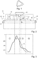
- the activated and thus recombination-active boron-oxygen correlated defects can be converted back into a recombination-inactive state by heating it to 100-200 or 100-300 ° C in the dark for a short time (see Figure 1 : Transition from active state B by annealing to inactive state A). With renewed illumination or charge carrier injection, however, the boron-oxygen correlated degradation takes place again, which is why the defects are also called metastable.
- the density of the (activated) defects depends roughly linearly on the boron concentration and roughly quadratically on the oxygen concentration in the silicon substrate.
- this effect therefore relates to boron-doped oxygen-rich silicon materials which were produced according to the Czochralski process.
- the efficiency can thereby be significantly reduced ( ⁇ 1% abs loss of efficiency). Specific degradation losses can vary depending on the architecture of the solar cell used.
- multicrystalline silicon materials with typically lower oxygen contamination show the effect, as do silicon materials in which boron is not the dominant dopant, in particular also phosphorus-doped partially compensated materials with boron admixtures.
- a first approach is to minimize the undesired oxygen contamination of the silicon crystal.
- novel coatings of the quartz crucible should prevent the same from dissolving.
- magnetic fields are mainly used in the Czochralski process, with which the convection movement of the silicon melt is suppressed directly on the quartz crucible, whereby the abrasion on the quartz crucible can be minimized.
- MCz silicon produced accordingly has correspondingly lower oxygen concentrations in the range 1 ⁇ 1017 to 5 ⁇ 1017 cm ⁇ 3.
- the manufacturing process is usually more expensive and more error-prone compared to the normal process.
- the second approach is based on reducing the boron concentration in the starting material.
- Theoretical calculations show that the efficiency potential without the restriction by boron-oxygen-correlated defects is maximal with doping around 1 ⁇ 1016 cm-3, whereas it is maximal only with lower doping if the boron-oxygen correlated degradation is taken into account.
- the maximum efficiency potential decreases with decreasing doping, so that less doped materials suffer lower degradation losses, but the maximum efficiency potential is not fully can be exploited.
- the optimal doping of the silicon substrate depends on the specific architecture of the solar cell. This approach in particular is currently being pursued by most manufacturers who use materials with boron concentrations in the range 1 ⁇ 1015 to 5 ⁇ 1015 cm-3 for oxygen-rich Cz silicon.
- the dopant boron is introduced by e.g. Replaced gallium. It could be shown that when using gallium either no corresponding defects arise or they are recombination inactive. However, in contrast to boron, gallium has a sub-optimal solubility behavior in crystal and melt, which makes it a technical challenge to produce a crystal that is homogeneously doped over the direction of crystallization. The result is greater material scrap and a higher susceptibility to errors in the process and thus higher costs. It is therefore questionable whether this approach is economically viable.
- the fourth approach takes advantage of the fact that the boron-oxygen correlated defect is not only found in an inactive one (see Figure 1 : State A) and an active state (see Figure 1 : State B) can exist, which can be converted into one another by charge carrier injection, ie degradation or heating in the dark, ie anneal, but also in a third, recombination-inactive "regenerated" state (see Figure 1 : State C), which, according to current knowledge, develops from the active state B through regeneration.
- This state is characterized in particular by the fact that (a) it has weak or negligible recombination activity and (b), in contrast to the initially present inactive state, is stable under illumination or charge carrier injection at temperatures ⁇ 150 ° C, ie there is no renewed activation of the Defects and thus degradation occurs.
- the transfer of the active defect, i.e. the state B, into the inactive third state C requires, according to current knowledge, a charge carrier injection e.g. by lighting or operating the solar cell in the forward direction at slightly increased temperatures in the range from 50 to 230 ° C, with higher temperatures or higher excess charge carrier densities accelerating the conversion of the defects.
- a charge carrier injection e.g. by lighting or operating the solar cell in the forward direction at slightly increased temperatures in the range from 50 to 230 ° C, with higher temperatures or higher excess charge carrier densities accelerating the conversion of the defects.
- the economy of the regeneration process depends essentially on the regeneration rate or the time required to bring a sufficiently large number of defects into the regenerated, advantageous state C. A process that can increase the regeneration rate and thus reduce the time required is therefore of great economic interest.
- the process step (d) corresponds precisely to the method according to this DE 10 2006 012 920 B3 .
- the method presented with the sub-steps (a) to (c) aims, among other things, at modifying a photovoltaic element in such a way that the in DE 10 2006 012 920 B3 described process optimized and thus economically attractive.
- the silicon substrate used in the method according to the invention can be a wafer which was produced according to the Czochralski method and has a boron doping in the range from 1 ⁇ 10 15 to 1 ⁇ 10 17 cm ⁇ 3.
- a wafer has a certain oxygen concentration of, for example, 1 ⁇ 1017 to 3 ⁇ 1018 cm ⁇ 3.
- other boron-doped, oxygen-containing silicon substrates can also be used, such as, for example, multicrystalline silicon wafers or silicon layers that have been deposited on a carrier from the gaseous or liquid phase.
- an emitter is formed according to the invention on the surface of the silicon substrate. This is a region which, as a rule, has a semiconductor type that is opposite to the semiconductor type of the substrate. If boron is the dominant dopant in the substrate, the substrate is p-doped. It cannot be ruled out that the semiconductor type of the substrate is n-type in spite of boron doping if corresponding amounts of n-doping substances such as phosphorus are present.
- the emitter can be formed, for example, by a superficial diffusion of dopants such as phosphorus (with p-type substrate) or boron (with n-type substrate).
- Such diffusion is typically carried out at temperatures above 800 ° C.
- other methods can also be used to produce a corresponding emitter layer.
- an emitter layer of corresponding polarity can be deposited on the substrate surface from a gaseous or liquid phase or a plasma.
- Another possibility for producing an emitter layer can be the alloying of appropriate substances.
- the surface of the silicon substrate does not have to be completely covered. It may be sufficient that only part of the surface on the front and / or back is covered with an emitter layer.
- the emitter and the substrate are of the same semiconductor type can also be implemented, e.g. if the substrate and the emitter layer have a very different band structure (heterostructures), so that a band bending occurs at the interface that results in the desired Causes potential gradient.
- a semiconductor does not even have to be used for this, since an appropriately selected metal can also lead to such band bending (MIS structures).
- Hydrogen can be introduced using a wide variety of methods.
- the hydrogen can consist of coatings applied on one or both sides such as hydrogenated silicon nitrides (a-SiNx: H), hydrogenated silicon carbides (a-SiCx: H), hydrogenated silicon oxides (a-SiOx: H), hydrogenated silicon oxynitrides (a -SiOxNy: H), hydrogenated aluminum oxides (Al2O3), hydrogenated amorphous silicon (a-Si: H) or comparable layers which can also have other functions (e.g. passivation of the surface, anti-reflective coating) are released and penetrate the silicon crystal.
- the exact parameters, in particular with regard to temperatures at which the hydrogen bound in the layer is released vary from layer to layer and are described in different embodiments. Corresponding analogous embodiments for comparable layers will be apparent to the person skilled in the art.
- this can be realized in the context of an alloying process of the metallic contacts of a solar cell, at which temperatures> 750 ° C exist for a few seconds.
- hydrogenated aluminum oxide (Al2O3) is used as the hydrogen source, which in the context of a temperature step at temperatures> 250 ° C. can release hydrogen which can penetrate the substrate.
- Al2O3 hydrogenated aluminum oxide
- the maximum temperature, temperature profile and duration must be selected accordingly in order to achieve a sufficiently high and well-distributed hydrogen concentration in the substrate.
- excess minority charge carriers are generated. This can be done, for example, by lighting or, for example, by introducing an external current.
- hydrogenated amorphous silicon (a-Si: H) is used as the hydrogen source, hydrogen being released in the context of a temperature step at temperatures> 100 ° C.
- silicon nitride layers and aluminum oxides must be selected accordingly, in order to achieve a sufficiently high and well-distributed hydrogen concentration in the substrate.
- excess minority charge carriers can be generated in the substrate during the temperature step. This can be done, for example, by lighting or, for example, by introducing an external current.
- multi-layer systems for example composed of the layers mentioned above, can also be used.
- the layer system can be designed in such a way that the layer adjacent to the substrate serves as a hydrogen source and at least one further layer is located on it.
- At least one of the further layers can act as a hydrogen diffusion barrier, ie this further layer is less permeable to hydrogen than the hydrogen-containing layer underneath and thus the hydrogen diffusion through this layer takes place only comparatively slowly as part of a high-temperature step.
- this layer serves as a hydrogen reflector and the hydrogen released from the hydrogen source is better retained in the substrate. This is advantageous because the yield of hydrogen from the source layer, ie the ratio from into the substrate diffused amount of hydrogen to released amount, in this case is better and, as mentioned later, also the out-diffusion is minimized at lower temperatures.
- the introduction of hydrogen into the substrate can also take place in other ways.
- the hydrogen can be implanted into the silicon substrate, i. protons are accelerated accordingly and shot onto or into the substrate.
- a hydrogen distribution in the substrate can be generated in a targeted manner.
- the actual ion implantation can be followed by a high temperature step> 500 ° C, which on the one hand is intended to heal any crystal damage that can occur when the protons are decelerated and, on the other hand, can also bring about a redistribution of the hydrogen.
- the introduction of the hydrogen into the substrate can also take place, for example, by diffusing atomic hydrogen from an atmosphere enriched with hydrogen or in a hydrogen-containing plasma.
- the hydrogen introduced remains in the substrate in sufficient quantity.
- the substrate reaches temperatures> 400 ° C, in particular> 450 ° C, is for a longer period, provided that no new hydrogen from the above or other sources is available, otherwise hydrogen effusion occurs to a significant extent.
- the time should be minimized in the temperature range in which the layer releases less hydrogen into the substrate than it effuses from the substrate.
- a-SiNx: H hydrogenated silicon nitride layers
- the embodiment with at least one diffusion barrier layer for hydrogen can be particularly advantageous, since the hydrogen itself is prevented from effusing from the substrate in the temperature range in question> 400 ° C or> 450 ° C. In this case, lower cooling rates greater than 0.3 K / s can still be acceptable.
- the substrate in the temperature range 230-450 ° C. for a certain period of at least 10 s, at most 30 min to hold. This can be implemented, for example, in the form of a plateau or, for example, in the form of a temperature ramp.
- the substrate is kept at a temperature in the range from 230 to 450 ° C. without generation of excess minority charge carriers, higher temperatures reducing the necessary holding time until the desired effect has been achieved.
- the substrate is then cooled down to room temperature with a steep temperature ramp.
- the substrate can then go through the regeneration process as in DE 10 2006 012 920 B3 are supplied as described.
- the substrate is kept at a temperature in the range from 230 to 450 ° C. without generation of excess minority charge carriers, with higher temperatures reducing the necessary holding time until the desired effect has been achieved.
- the substrate is transferred to the temperature range from 50 to 230 ° C, in which the regeneration process is analogous to that in DE 10 2006 012 920 B3 described can run.
- the substrate is at a temperature with generation of excess minority charge carriers, for example by lighting be kept in the range of 230..450 ° C, with higher temperatures reducing the necessary holding time until the desired effect is achieved.
- partial or complete regeneration can also occur at temperatures> 230 ° C under certain circumstances.
- the substrate is transferred to the temperature range of 50 to 230 ° C, in which the regeneration process continues if necessary, which can run faster due to the regeneration that has already taken place.
- hydrogenated silicon nitride is used as the hydrogen source, the layer being applied to a silicon wafer only on one side, while the opposite side is covered over the entire area by aluminum.
- silicon nitride layer which also functions as an anti-reflection coating and passivation layer, there is a metallic paste applied locally, for example by means of screen printing, which attacks the silicon nitride layer at high temperatures and thus makes contact with the silicon below.
- the release of the hydrogen from the silicon nitride layer takes place within the framework of a typical alloying process of metallization of the photovoltaic element, which typically takes place above 750 ° C. in a belt furnace.
- a device in the form of a specially designed continuous furnace 10 is shown, which can be used for treating a silicon substrate in the context of the production of a solar cell and which is designed to carry out an embodiment of the production method described herein and in particular the stabilization treatment step to be carried out.
- the conveyor furnace 10 has a belt 14 that can be moved by driven rollers 12. At an inlet side 16, silicon substrates can be placed on the belt 14 and then be driven by means of the belt 14 through differently heated zones of the continuous furnace 10.
- the silicon substrates can previously have been provided with a hydrogen-containing layer on their surface.
- a pattern of metal-containing paste can have been printed onto this hydrogen-containing layer, whereby the metal contacts for the solar cell are ultimately to be formed.
- One or more radiant heaters 20 are arranged in a preheating zone 18, with the aid of which the silicon substrates transported on the belt 14 can be preheated to temperatures of up to above 500.degree.
- At least one further radiant heater 24 is provided, with the aid of which silicon substrates passing through can be briefly heated to temperatures of up to above 700 ° C.
- cooling zone 26 This is followed by a cooling zone 26.
- this cooling zone 26 not only is preferably no radiant heater provided, but a cooling device 28 is even provided, with the aid of which the silicon substrates passing through can be actively cooled.
- the cooling device can be designed, for example, as a fan for blowing cool nitrogen gas into the cooling zone 26.
- a temperature holding zone 30 can then follow.
- a further radiant heater 32 is provided in this temperature holding zone 30, with the aid of which the temperature of the silicon substrates can be kept within the temperature holding zone 30 in a range from 230 ° C. to 450 ° C.
- a length of the temperature holding zone 30 can be dimensioned such that, at a given throughput speed, a silicon substrate transported by the belt 14 needs at least about 10 seconds to be transported through the temperature holding zone 30, with the aid of the radiant heater 32 at a desired temperature within the Temperature range from 230 to 450 ° C is held.
- the temperature holding zone 30 can for example be at least as long, preferably at least three times, preferably at least six times longer than the maximum heating zone 22.
- the entire continuous furnace can, for example, be more than twice as long as a conventional continuous furnace without a temperature holding zone 30.
- a strong light source 36 for example in the form of a laser with a widened laser beam or in the form of a strong lamp with wavelengths that can be absorbed by the silicon substrate, can be provided to illuminate the silicon substrates passing through with exposure intensities of at least 0.3 kW / m2 to illuminate. Since the silicon substrates are still at a temperature well above 90 ° C., at least at the beginning of the cooling zone 34, this can bring about the regeneration process and the efficiency of the solar cells ultimately produced can be stabilized.
- a light source can also be provided in the temperature holding zone 30 (in the case of the in Fig. 2 shown embodiment not provided).
- a light source can also be provided in the temperature holding zone 30 (in the case of the in Fig. 2 shown embodiment not provided).
- suitable lighting of the silicon substrates already in the temperature holding zone 30 it can possibly be supported that hydrogen which has penetrated into the silicon substrates assumes a state that is advantageous for a subsequent regeneration.
- regeneration within the silicon substrates can be carried out at least partially or, if the process is carried out appropriately, also completely, by means of suitable lighting already within the temperature holding zone 30.
- All of the described components of the continuous furnace 10 can preferably be controlled by a common controller 40.
- the silicon substrates After the silicon substrates have passed through the entire continuous furnace 10, they can be removed from an outlet side 38 and subjected to further processing or characterization steps.
- the wafer serving as silicon substrate When entering the belt furnace and passing through the preheating zone 18 (zone 1), the wafer serving as silicon substrate is first heated up to around 650 ° C, hydrogen is released from the hydrogenated silicon nitride layer previously deposited on it and the diffusion into the wafer begins (zone 2). After reaching the maximum temperature in the maximum heating zone 22, the release of hydrogen from the silicon nitride layer decreases again. At the same time, some of the hydrogen that has diffused into the wafer is already effusing again. If the temperature falls below about 650 ° C., the effusion from the wafer outweighs the release of hydrogen from the silicon nitride layer or the diffusion into the wafer and the hydrogen content of the wafer decreases again.
- the wafer is cooled down in the cooling zone 26 (zone 3) with a steep temperature ramp at a high cooling rate of, for example, more than 20 K / s and further hydrogen effusion is suppressed.
- the wafer is held in the temperature range of 230 to 450 ° C and, according to the method described, the process starts which increases the regeneration rate, which is shown in a later regeneration process step.
- the regeneration time required later can be shortened by a generation of excess charge carriers, for example by lighting in zone 4.
- a typical temperature profile when passing through a conventional continuous furnace is also shown as a dashed line 42. It can be seen that the silicon substrates cool continuously and approximately linearly after reaching a maximum temperature.
- a dwell time within the temperature range of above 450 ° C is significantly longer than in the continuous furnace according to the invention, whereas a dwell time within the temperature range of between 230 ° C and 450 ° C is significantly shorter than in the continuous furnace according to the invention.
- the inventors assume that hydrogen, in particular its amount, its bond state and charge state in the silicon crystal, have a decisive influence has the conversion of the recombination-active defects into the third, regenerated state (state C), for example through the addition of hydrogen to the defect. Since there is usually no or too little hydrogen in the silicon crystal immediately after the crystal growth, hydrogen must first be introduced into the crystal in order to enable a conversion into the regenerated state.
- various hydrogen sources can be used, as described above.
- the inventors assume that the origin of the hydrogen is of minor importance in the context of this model, as long as there is a sufficiently high concentration in the crystal of the silicon substrate in the temperature range below about 450 ° C and a sufficiently homogeneous distribution laterally and in depth . Above about 400 or 450 ° C, hydrogen can still escape to a significant extent from the silicon crystal into the environment.
- the described manufacturing process according to the invention takes this into account in that the solar cell in the manufacturing process is only as briefly as possible in a temperature range> 400 or> 450 ° C, in which the hydrogen diffuses out, but not new hydrogen e.g. is delivered from one shift.
- the bond state or charge state of the hydrogen is of decisive importance. Accordingly, in the temperature range below about 500 ° C, the hydrogen could largely exist in at least two different bond states, for example in the form of H2 molecules or bonded to boron atoms as BH pairs. However, hydrogen in such a bound form would not be sufficiently mobile.
- the regeneration in this description would correspond to a detachment of the hydrogen, the subsequent diffusion in atomic form and the attachment to a boron-oxygen-correlated defect.
- the regeneration rate i.e.
- the regeneration process depends, among other things, on how easily the hydrogen can free itself from its bound state, either purely thermally supported or through a change in the state of charge.
- the described manufacturing process according to the invention can possibly ensure that hydrogen is only slightly bound (at least with charge carrier injection) in sufficient quantity and is thus available for the regeneration process.
- the mobility of atomic hydrogen after it has been split off depends on its state of charge. In p-type silicon, the hydrogen is usually positively charged and its diffusion is hindered by electrostatic interaction in the crystal lattice. If, on the other hand, the hydrogen is in a neutral state of charge, its mobility is significantly higher.
Description
Die vorliegende Erfindung betrifft ein Verfahren zum Herstellen eines Photovoltaikelements mit einem durch einen Stabilisierungsbehandlungsschritt stabilisierten Wirkungsgrad. Insbesondere betrifft die vorliegende Erfindung ein Verfahren zum Herstellen einer Solarzelle auf Basis eines Bor-dotierten, Sauerstoff-haltigen Siliziumsubstrats. Ferner betrifft die Erfindung eine Vorrichtung zum Behandeln eines Siliziumsubstrats im Rahmen einer Herstellung eines Photovoltaikelements, wobei die Vorrichtung dazu ausgebildet ist, den Stabilisierungsbehandlungsschritt des erfindungsgemäßen Verfahrens auszuführen.The present invention relates to a method for manufacturing a photovoltaic element with an efficiency stabilized by a stabilization treatment step. In particular, the present invention relates to a method for producing a solar cell based on a boron-doped, oxygen-containing silicon substrate. The invention also relates to a device for treating a silicon substrate in the course of producing a photovoltaic element, the device being designed to carry out the stabilization treatment step of the method according to the invention.
Solarzellen dienen als photovoltaische Elemente dazu, Licht in elektrischen Strom umzuwandeln. Lichtgenerierte Ladungsträgerpaare, welche beispielsweise an einem pn-Übergang zwischen einem Emitterbereich und einem Basisbereich räumlich getrennt wurden, müssen dabei mithilfe von elektrischen Kontakten der Solarzelle einem äußeren Stromkreis zugeleitet werden. Es müssen hierzu elektrische Kontaktanordnungen sowohl an dem Emitter als auch an der Basis der Solarzelle vorgesehen werden.Solar cells serve as photovoltaic elements to convert light into electricity. Light-generated charge carrier pairs, which have been spatially separated at a pn junction between an emitter area and a base area, for example, have to be fed to an external circuit with the aid of electrical contacts of the solar cell. For this purpose, electrical contact arrangements must be provided both on the emitter and on the base of the solar cell.
Solarzellen werden heute meist auf Basis von Silizium als Halbleitersubstratmaterial gefertigt. Siliziumsubstrate werden dabei häufig in Form monokristalliner oder multikristalliner Wafer bereitgestellt. Es wurde vielfach beobachtet, dass bei Solarzellen, die auf Basis kristalliner Siliziumwafer hergestellt sind, Degradationseffekte auftreten können, die den Wirkungsgrad der Solarzelle mit der Zeit reduzieren. Signifikante Wirkungsgradverluste von bis zu über 1%abs wurden beobachtet.Today solar cells are mostly manufactured on the basis of silicon as the semiconductor substrate material. Silicon substrates are often provided in the form of monocrystalline or multicrystalline wafers. It has often been observed that in solar cells that are manufactured on the basis of crystalline silicon wafers, degradation effects can occur which reduce the efficiency of the solar cell over time. Significant efficiency losses of up to over 1% abs have been observed.
In der
Allerdings wurde bisher davon ausgegangen, dass Prozessdauern, während derer ein Siliziumsubstrat einem Stabilisierungsbehandlungsschritt unterzogen werden muss, verhältnismäßig lang sein sollten, um eine ausreichende Stabilisierung des Wirkungsgrades erreichen zu können. Dies kann insbesondere bei einer automatisierten industriellen Fertigungslinie zu Verzögerungen und somit zur Bildung eines Flaschenhalses in der Produktion führen.However, it has hitherto been assumed that process times during which a silicon substrate has to be subjected to a stabilization treatment step should be relatively long in order to be able to achieve adequate stabilization of the efficiency. In the case of an automated industrial production line in particular, this can lead to delays and thus to the formation of a bottleneck in production.
Weitere Informationen zu Möglichkeiten, Solarzellen herzustellen und dabei eventuell Wirkungsgrade zu beeinflussen oder zu stabilisieren, sind unter anderem angegeben in:
-
LIM BIANCA ET AL: "Solar cells on low-resistivity boron-doped Czochralski-grown silicon with stabilized efficiencies of 20%", APPLIED PHYSICS LETTERS, Bd. 93, Nr. 16, 20. Oktober 2008 (2008-10-20), Seiten 162102, XP012111972, ISSN: 0003-6951, DOI: 10.1063/1.3003871 -
W1LK1NGS ET AL: "Influence of hydrogen on the regeneration of boron-oxygen related defects in crystalline silicon", JOURNAL OF APPLIED PHYSICS, Bd. 113, Nr. 19, 21. Mai 2013 (2013-05-21), Seiten 194503-194503, XP012174152, ISSN: 0021-8979, DOI: 10.1063/1.4804310 -
GEORG KRUGEL ET AL: "Impact of Hydrogen Concentration on the Regeneration of Light Induced Degradation", ENERGY PROCED1A, Bd. 8, 17. April 2011 (2011-04-17), - 20. April 2011 (2011-04-20), SEITEN 47-51, XP028263042, ISSN: 1876-6102, DOI: 10.1016/J.EGYPR0.2011.06.100 -
R. S∅NDENÄ ET AL: "LIGHT INDUCED DEGRADATION IN MONOCRYSTALLINE SILICON WAFERS MADE FROM THE METALLURGICAL ROUTE", PROCEEDINGS OF THE 25TH EUPVSEC, 6. SEPTEMBER 2010 (2010-09-06), - 10. SEPTEMBER 2010 (2010-09-10), SEITEN 1586-1590, XP040531032, VALENCIA-SPAIN DOI: 10.4229/25thEUPVSEC2010-2CV.1.45 ISBN: 978-3-936338-26-3 -
FR 2 949 607 A1 -
US 2013/102129 A1 -
EP 2 863 413 A2 -
FR 2 966 980 A1
-
LIM BIANCA ET AL: "Solar cells on low-resistivity boron-doped Czochralski-grown silicon with stabilized efficiencies of 20%", APPLIED PHYSICS LETTERS, Vol. 93, No. 16, October 20, 2008 (2008-10-20) , Pages 162102, XP012111972, ISSN: 0003-6951, DOI: 10.1063 / 1.3003871 -
W1LK1NGS ET AL: "Influence of hydrogen on the regeneration of boron-oxygen related defects in crystalline silicon", JOURNAL OF APPLIED PHYSICS, Vol. 113, No. 19, May 21, 2013 (2013-05-21), pages 194503- 194503, XP012174152, ISSN: 0021-8979, DOI: 10.1063 / 1.4804310 -
GEORG KRUGEL ET AL: "Impact of Hydrogen Concentration on the Regeneration of Light Induced Degradation", ENERGY PROCED1A, Vol. 8, April 17, 2011 (2011-04-17), - April 20, 2011 (2011-04-20) , PAGES 47-51, XP028263042, ISSN: 1876-6102, DOI: 10.1016 / J.EGYPR0.2011.06.100 -
R. S∅NDENÄ ET AL: "LIGHT INDUCED DEGRADATION IN MONOCRYSTALLINE SILICON WAFERS MADE FROM THE METALLURGICAL ROUTE", PROCEEDINGS OF THE 25TH EUPVSEC, SEPTEMBER 6, 2010 (2010-09-06), - SEPTEMBER 10, 2010 (2010-09 -10), PAGES 1586-1590, XP040531032, VALENCIA-SPAIN DOI: 10.4229 / 25thEUPVSEC2010-2CV.1.45 ISBN: 978-3-936338-26-3 -
FR 2 949 607 A1 -
US 2013/102129 A1 -
EP 2 863 413 A2 -
FR 2 966 980 A1
Es kann daher ein Bedarf an einem verbesserten Verfahren zum Herstellen eines Photovoltaikelements mit stabilisiertem Wirkungsgrad bestehen. Insbesondere kann ein Bedarf an einem solchen Verfahren bestehen, welches eine Wirkungsgradstabilisierung innerhalb kurzer Prozessdauern ermöglicht. Ferner kann ein Bedarf an einer Vorrichtung zum Behandeln eines Siliziumsubstrats im Rahmen einer Herstellung eines Photovoltaikelements bestehen, welche insbesondere die Durchführung des Stabilisierungsbehandlungsschritts des beschriebenen Verfahrens ermöglicht.There may therefore be a need for an improved method of manufacturing a photovoltaic element with stabilized efficiency. In particular, a There is a need for such a method which enables efficiency to be stabilized within short process times. Furthermore, there may be a need for a device for treating a silicon substrate in the context of the production of a photovoltaic element, which in particular enables the stabilization treatment step of the described method to be carried out.
Ein solcher Bedarf kann mit dem Verfahren bzw. der Vorrichtung gemäß den unabhängigen Ansprüchen erfüllt werden. Ausführungsformen der Erfindung sind in den abhängigen Ansprüchen sowie der nachfolgenden Beschreibung dargestellt.Such a need can be met with the method and the device according to the independent claims. Embodiments of the invention are presented in the dependent claims and the description below.
Gemäß einem ersten Aspekt der vorliegenden Erfindung, wie in Anspruch 1 definiert, wird ein Verfahren zum Herstellen eines Photovoltaikelements mit stabilisiertem Wirkungsgrad beschrieben, welches die folgenden Schritte aufweist: Es wird ein Siliziumsubstrat bereitgestellt. An einer Oberfläche des Siliziumsubstrats wird eine Emitterschicht ausgebildet. Ferner werden an dem Siliziumsubstrat elektrische Kontakte ausgebildet. Das Verfahren zeichnet sich dadurch aus, dass ergänzend ein Stabilisierungsbehandlungsschritt durchgeführt wird. Dieser umfasst ein gezieltes Einbringen von Wasserstoff in das Siliziumsubstrat. Nachdem der Wasserstoff in das Siliziumsubstrat eingebracht wurde, werden in dem Siliziumsubstrat Überschussminoritätsladungsträger erzeugt, während das Siliziumsubstrat auf einer Temperatur von über 230°C ist. Der Wasserstoff wird bei Temperaturen oberhalb von 650°C eingebracht und eine anschließende Abkühlung bis auf 450°C wird mit einer Rampe mit einer Abkühlrate oberhalb 550°C von mindestens 10 K/s durchgeführt.According to a first aspect of the present invention as defined in
Gemäß einem zweiten Aspekt der vorliegenden Erfindung, wie in Anspruch 12 definiert, wird eine Vorrichtung zum Behandeln eines Siliziumsubstrats im Rahmen einer Herstellung eines Photovoltaikelements beschrieben, wobei die Vorrichtung dazu ausgebildet ist, den Stabilisierungsbehandlungsschritt des erfindungsgemäßen Verfahrens durchzuführen.According to a second aspect of the present invention, as defined in
Die Vorrichtung ist als Durchlaufofen mit einer Mehrzahl unterschiedlich temperierbarer Zonen ausgebildet und weist eine Beleuchtungseinrichtung auf, mit Hilfe derer Minoritätsladungsträger in dem Siliziumsubstrat erzeugt werden können. Die Zonen können dabei derart temperierbar sein und die Vorrichtung einschließlich der Beleuchtungseinrichtung derart ausgebildet sein, dass ein den Durchlaufofen durchlaufendes Siliziumsubstrat in einer Hochtemperaturzone zunächst kurzzeitig auf eine Temperatur von oberhalb 650°C erhitzt wird, dann in einer Abkühlzone mit einer Abkühlrate oberhalb 550°C von mindestens 10 K/s auf eine Temperatur unterhalb von 450°C abgekühlt wird und dann in einer Temperaturhaltezone bei einer Temperatur von zwischen 230°C und 450°C gehalten wird, optional für wenigstens 10s, und gleichzeitig oder nachfolgend das Siliziumsubstrat bei einer Temperatur von über 230°C, mit einer Beleuchtungsintensität größer 0,3 kW/m2 beleuchtet wird.The device is designed as a continuous furnace with a plurality of differently temperature-controllable zones and has a lighting device on, with the help of which minority charge carriers can be generated in the silicon substrate. The zones can be tempered in such a way and the device including the lighting device can be designed in such a way that a silicon substrate passing through the continuous furnace is first briefly heated in a high-temperature zone to a temperature above 650 ° C, then in a cooling zone at a cooling rate above 550 ° C is cooled from at least 10 K / s to a temperature below 450 ° C and is then held in a temperature holding zone at a temperature of between 230 ° C and 450 ° C, optionally for at least 10s, and simultaneously or subsequently the silicon substrate at a temperature of over 230 ° C, is illuminated with a lighting intensity greater than 0.3 kW / m 2 .
Ohne den Schutzbereich der Erfindung einzuschränken, können Ideen zu Ausführungsformen des erfindungsgemäßen Verfahrens bzw. der erfindungsgemäßen Vorrichtung als unter anderem auf den nachfolgend beschriebenen Gedanken und Erkenntnissen beruhend angesehen werden:
Die Möglichkeit, ein im Rahmen der Herstellung eines Photovoltaikelements verwendetes Siliziumsubstrat mittels eines geeigneten Stabilisierungsbehandlungsschrittes gegen eine nachfolgende, im Betrieb des Photovoltaikelements ansonsten auftretende Degradation zu schützen bzw. zu stabilisieren, manchmal auch als Regeneration bezeichnet, ist seit längerem bekannt. Details dazu, wie ein Stabilisierungsbehandlungsschritt durchgeführt werden kann und welche Wirkungsmechanismen dahinter vermutet werden, wurden ausführlich in der
The possibility of protecting or stabilizing a silicon substrate used in the production of a photovoltaic element by means of a suitable stabilization treatment step against subsequent degradation otherwise occurring during operation of the photovoltaic element, sometimes also referred to as regeneration, has long been known. Details on how a stabilization treatment step can be carried out and what mechanisms of action are suspected behind it have been extensively provided in the
Es wurde nun erkannt, dass mithilfe zusätzlicher Prozessschritte oder geeignet gewählter Prozessparameter die Regenerationsrate während des Stabilisierungsbehandlungsschritts erheblich erhöht werden kann und somit die Dauer, über die der Stabilisierungsbehandlungsschritt durchgeführt werden sollte, um eine ausreichende Wirkungsgradstabilisierung für das letztendlich hergestellte Photovoltaikelement zu erreichen, möglichst kurz gehalten werden kann.It has now been recognized that with the aid of additional process steps or suitably selected process parameters, the regeneration rate can be increased significantly during the stabilization treatment step and thus the duration over which the Stabilization treatment step should be carried out in order to achieve sufficient efficiency stabilization for the photovoltaic element ultimately produced, can be kept as short as possible.
Insbesondere wurde beobachtet, dass eine Regenerationsrate maßgeblich davon abzuhängen scheint, welche Mengen an Wasserstoff in dem Siliziumsubstrat während des eigentlichen Regenerierungsvorganges, das heißt während Überschussminoritätsladungsträger bei erhöhter Substrattemperatur in dem Siliziumsubstrat erzeugt werden, vorhanden sind. Ferner scheint wichtig zu sein, wie der Wasserstoff innerhalb des Siliziumsubstrats verteilt ist und in welchem Bindungszustand sich dieser Wasserstoff innerhalb des Siliziumsubstrats befindet.In particular, it was observed that a regeneration rate appears to be largely dependent on the amounts of hydrogen present in the silicon substrate during the actual regeneration process, that is, while excess minority charge carriers are generated in the silicon substrate at an increased substrate temperature. In addition, it seems to be important how the hydrogen is distributed within the silicon substrate and in what bonding state this hydrogen is within the silicon substrate.
Es wird daher vorgeschlagen, zunächst gezielt Wasserstoff in das Siliziumsubstrat einzubringen. Dies kann, wie weiter unten detaillierter beschrieben, auf unterschiedliche Weise erfolgen. Anschließend hat es sich als vorteilhaft herausgestellt, das Siliziumsubstrat zumindest kurzzeitig, beispielsweise über wenigstens 5s oder wenigstens 10s, innerhalb eines Temperaturbereichs von 230°C bis 450°C zu halten. Eine Haltedauer scheint dabei umso kürzer wählbar zu sein, je höher die gehaltene Temperatur des Siliziumsubstrats ist. Es wird vermutet, dass dieses Halten des Siliziumsubstrats bei erhöhter Temperatur sich vorteilhaft auf den Bindungszustand des zuvor eingebrachten Wasserstoffs auswirkt. Anschließend kann der eigentliche Regenerationsvorgang durchgeführt werden, indem Überschussminoritätsladungsträger in dem Siliziumsubstrat erzeugt werden, während dieses auf einer erhöhten Temperatur von wenigstens mehr als 230°C und vorzugsweise jedoch weniger als 450°C, gehalten wird. Gegebenenfalls können die Überschussminoritätsladungsträger in dem Siliziumsubstrat bereits während des zuvor beschriebenen Haltens des Siliziumsubstrats innerhalb des Temperaturbereichs von zwischen 230°C und 450°C erzeugt werden.It is therefore proposed to first introduce hydrogen in a targeted manner into the silicon substrate. This can be done in different ways, as described in more detail below. It has subsequently been found to be advantageous to keep the silicon substrate at least briefly, for example for at least 5s or at least 10s, within a temperature range of 230 ° C. to 450 ° C. A holding period seems to be selectable the shorter the higher the temperature of the silicon substrate that is held. It is assumed that this holding of the silicon substrate at an elevated temperature has an advantageous effect on the bonding state of the previously introduced hydrogen. The actual regeneration process can then be carried out in that excess minority charge carriers are generated in the silicon substrate while the latter is kept at an elevated temperature of at least more than 230.degree. C. and preferably less than 450.degree. If appropriate, the excess minority charge carriers can be generated in the silicon substrate while the silicon substrate is being held within the temperature range of between 230 ° C. and 450 ° C. as described above.
Es wurde beobachtet, dass durch das gezielte Einbringen von Wasserstoff und das anschließende Regenerieren bei erhöhter Temperatur der Regenerationsvorgang erheblich beschleunigt werden kann. Statt, wie bisher vermutet, wenigstens mehrere Minuten hierfür zu benötigen, wird davon ausgegangen, dass die Regeneration innerhalb weniger Sekunden durchgeführt werden kann und der gesamte Stabilisierungsbehandlungsschritt somit geeignet innerhalb einer einzigen Vorrichtung wie beispielsweise einem Durchlaufofen durchgeführt werden kann.It has been observed that the targeted introduction of hydrogen and the subsequent regeneration at an elevated temperature can significantly accelerate the regeneration process. Instead of taking at least several minutes for this, as previously assumed, it is assumed that the regeneration can be carried out within a few seconds and the entire stabilization treatment step can thus be carried out appropriately within a single device such as a continuous furnace.
Dies kann beispielsweise ermöglichen, innerhalb einer häufig industriell eingesetzten Herstellungssequenz, bei der Siebdruckkontakte in einem Durchlaufofen eingefeuert werden, den Durchlaufofen derart zu modifizieren, dass gleichzeitig auch der Stabilisierungsbehandlungsschritt durchgeführt werden kann. Mittels eines solchen geeignet modifizierten Durchlaufofens kann somit sowohl eine Kontaktbildung durch Einfeuern siebgedruckter Metallpastenstrukturen als auch eine Regeneration des Siliziumsubstrats und somit eine Stabilisierung des Wirkungsgrads der letztendlich hergestellten Solarzelle simultan durchgeführt werden.This can make it possible, for example, within a manufacturing sequence that is frequently used industrially, in which screen-printed contacts are fired in a continuous furnace, to modify the continuous furnace in such a way that the stabilization treatment step can also be carried out at the same time. By means of such a suitably modified continuous furnace, both a contact formation by firing screen-printed metal paste structures and a regeneration of the silicon substrate and thus a stabilization of the efficiency of the solar cell ultimately produced can be carried out simultaneously.
Der Wasserstoff wird bei Temperaturen oberhalb von 650°C, eingebracht und eine anschließende Abkühlung bis auf 450°C wird mit einer Rampe mit einer Abkühlrate oberhalb 550°C von mindestens 10 K/s, vorzugsweise mindestens 20 K/s, stärker bevorzugt mindestens 30 K/s und noch stärker bevorzugt mindestens 60 K/s durchgeführt. Mit anderen Worten kann das Siliziumsubstrat zunächst auf über 650°C erhitzt werden, um den Wasserstoff einzutreiben, und dann schnell auf unter 450°C abgekühlt werden, wobei zumindest die Abkühlung bis auf 550°C besonders rapide erfolgen soll mit einer Abkühlrate von wenigstens 10 K/s.The hydrogen is introduced at temperatures above 650 ° C and a subsequent cooling down to 450 ° C is ramped with a cooling rate above 550 ° C of at least 10 K / s, preferably at least 20 K / s, more preferably at least 30 K / s and even more preferably at least 60 K / s. In other words, the silicon substrate can first be heated to over 650 ° C in order to drive in the hydrogen, and then quickly cooled to below 450 ° C, whereby at least the cooling down to 550 ° C should take place particularly rapidly with a cooling rate of at least 10 K / s.
Wasserstoff kann bei hohen Temperaturen von deutlich über 450°C, insbesondere über 550°C, sehr schnell, das heißt innerhalb weniger Sekunden oder Sekundenbruchteile, in das Siliziumsubstrat eindiffundieren und sich in diesem vorzugsweise möglichst homogen verteilen. Beispielsweise kann Wasserstoff aus einer auf dem Siliziumsubstrat aufgebrachten wasserstoffhaltigen Schicht bei ausreichend hohen Temperaturen schnell in das darunterliegende Siliziumsubstrat eindiffundieren.At high temperatures of well over 450 ° C, in particular over 550 ° C, hydrogen can be converted very quickly, i.e. within a few seconds or fractions of a second Diffuse into the silicon substrate and preferably distribute them as homogeneously as possible. For example, hydrogen can quickly diffuse into the underlying silicon substrate from a hydrogen-containing layer applied to the silicon substrate at sufficiently high temperatures.
Allerdings wurde die Gefahr erkannt, dass für den Fall, dass die hohen Temperaturen zu lange vorherrschen und sich die Wasserstoffquelle mit der Zeit erschöpft, Wasserstoff auch wieder aus dem Siliziumsubstrat herausdiffundieren kann, das heißt, dass es zu einer Effusion von Wasserstoff kommen kann. Insbesondere an der Oberfläche des Siliziumsubstrats, das heißt, dort wo sich bei der fertigen Solarzelle beispielsweise die Emitterschicht befindet und die Solarzelle somit besonders empfindlich gegenüber defekt-begründeten Degradationseffekten ist, kann es zu einer Verarmung von Wasserstoff kommen. Da der Wasserstoff eine nachfolgend durchzuführende Regeneration maßgeblich zu unterstützen scheint, sollte daher eine Wasserstoffeffusion möglichst weitgehend vermieden werden.However, the danger has been recognized that in the event that the high temperatures prevail for too long and the hydrogen source is exhausted over time, hydrogen can also diffuse out of the silicon substrate again, which means that there can be an effusion of hydrogen. Hydrogen depletion can occur particularly on the surface of the silicon substrate, i.e. where the emitter layer is located in the finished solar cell and the solar cell is therefore particularly sensitive to degradation effects caused by defects. Since the hydrogen appears to significantly support a regeneration to be carried out subsequently, hydrogen effusion should therefore be avoided as far as possible.
Es wird daher vorgeschlagen, nach einem Einbringen von Wasserstoff bei ausreichend hoher Temperatur, die Temperatur sehr schnell zu reduzieren, das heißt, das Siliziumsubstrat mit einer hohen Abkühlrate bis unter 450°C abzukühlen, um den Zeitraum, innerhalb dessen Wasserstoff aus dem Siliziumsubstrat herausdiffundieren könnte, möglichst kurz zu halten. Ein solches schnelles Abkühlen ist insbesondere dann anzustreben, wenn die Wasserstoffquelle zu erschöpfen droht, d.h. kein Wasserstoff z.B. nach einer zu langen Hochtemperaturphase mehr nachgeliefert werden kann, oder wenn die Wasserstoffquelle z.B. wegen zu geringer Temperaturen keinen Wasserstoff mehr freisetzen kann.It is therefore proposed, after introducing hydrogen at a sufficiently high temperature, to reduce the temperature very quickly, that is, to cool the silicon substrate at a high cooling rate to below 450 ° C. in order to allow the period of time within which hydrogen could diffuse out of the silicon substrate to keep it as short as possible. Such rapid cooling is particularly desirable when the hydrogen source threatens to be exhausted, i.e. no hydrogen e.g. after too long a high temperature phase more can be delivered, or if the hydrogen source e.g. can no longer release hydrogen because the temperature is too low.
Nachfolgend kann das Siliziumsubstrat dann bei Temperaturen von unterhalb 450°C ausreichend lange gehalten werden, wobei bei diesen verhältnismäßig niedrigen Temperaturen eine Effusion von Wasserstoff kaum auftritt, der Wasserstoff vermutlich aber einen für eine Regeneration förderlichen Bindungszustand innerhalb des Siliziumsubstrats einnehmen kann.Subsequently, the silicon substrate can then be kept for a sufficiently long time at temperatures below 450 ° C., with hydrogen effusion hardly occurring at these relatively low temperatures, but hydrogen presumably can assume a bonding state within the silicon substrate that is conducive to regeneration.
Gemäß einer Ausführungsform können die Überschussminoritätsladungsträger während der Regeneration durch Beleuchten mit einer Beleuchtungsintensität größer 0,3 kW/m2, vorzugsweise größer 1 kW/m2, stärker bevorzugt größer 3 kW/m2 mit Licht mit Wellenlängen kleiner als 1180 nm erzeugt werden.According to one embodiment, the excess minority charge carriers can be generated during the regeneration by lighting with an illumination intensity greater than 0.3 kW / m 2 , preferably greater than 1 kW / m 2 , more preferably greater than 3 kW / m 2 with light with wavelengths less than 1180 nm.
Es wurde beobachtet, dass eine Regeneration umso schneller erfolgt, das heißt eine Regenerationsrate umso größer ist, je höher eine Dichte an Überschussminoritätsladungsträgern ist. Überschussminoritätsladungsträger können unter anderem durch Beleuchtung innerhalb des Siliziumsubstrats generiert werden. Eine hohe Beleuchtungsintensität kann somit eine schnelle Regeneration unterstützen.It was observed that a regeneration takes place all the faster, that is to say the higher the density of excess minority charge carriers, the greater the regeneration rate. Excess minority charge carriers can be generated, among other things, by lighting within the silicon substrate. A high level of lighting can therefore support rapid regeneration.
Gemäß einer Ausführungsform können die Überschussminoritätsladungsträger bei einer Temperatur des Siliziums von zwischen 230°C und 450°C, vorzugsweise zwischen 230°C und 400°C und stärker bevorzugt zwischen 230°C und 350°C und noch stärker bevorzugt zwischen 230°C und 300°C erzeugt werden.According to one embodiment, the excess minority charge carriers can be used at a temperature of the silicon of between 230 ° C and 450 ° C, preferably between 230 ° C and 400 ° C and more preferably between 230 ° C and 350 ° C and even more preferably between 230 ° C and 300 ° C can be generated.
Während bisher davon ausgegangen wurde, dass eine Regenerationsrate zwar zunächst mit zunehmender Temperatur oberhalb von 50°, insbesondere oberhalb von 90°C ansteigt, oberhalb von etwa 180°C dann aber wieder abzunehmen schien, vermutlich aufgrund konkurrierender Effekte, wurde nun erkannt, dass durch ein vorheriges Einbringen von Wasserstoff und optional ein anschließendes Halten des Siliziumsubstrats bei geeigneter Temperatur über eine geeignet lange Zeitdauer das Siliziumsubstrat offenbar derart vorbehandelt werden kann, dass ein Regenerationsvorgang auch bei höheren Temperaturen oberhalb von 230°C durchgeführt werden kann. Mit höherer Temperatur scheint dabei eine Regeneration schneller abzulaufen. Entgegenwirkende, konkurrierende Effekte scheinen durch den zuvor eingebrachten Wasserstoff und die Temperaturvorbehandlung schwächer auszufallen oder deutlich langsamer zu wirken als die aufgrund der Vorbehandlung beschleunigt ablaufenden, die Regeneration bewirkenden Effekte. Daher scheinen diese konkurrierenden Effekte erst bei wesentlich höheren Temperaturen von beispielsweise deutlich über 300°C den Regenerationseffekten erheblich entgegenzuwirken. Insgesamt kann somit eine Regeneration des Siliziumsubstrats aufgrund der Vorbehandlung und der dadurch ermöglichten wesentlich höheren Temperaturen während des eigentlichen Regenerationsvorgangs erheblich beschleunigt werden.While it was previously assumed that a regeneration rate initially rises with increasing temperature above 50 °, in particular above 90 ° C, but then seemed to decrease again above about 180 ° C, probably due to competing effects, it has now been recognized that through a prior introduction of hydrogen and optionally a subsequent holding of the silicon substrate at a suitable temperature for a suitable long period of time, the silicon substrate can evidently be pretreated in such a way that a regeneration process can also be carried out at higher temperatures above 230.degree. With a higher temperature, regeneration seems to run faster. Counteracting, competing effects appear due to the previously introduced hydrogen and the temperature pretreatment, to be weaker or to act significantly more slowly than the effects that bring about regeneration, which are accelerated due to the pretreatment. Therefore, these competing effects only seem to counteract the regeneration effects significantly at significantly higher temperatures, for example well over 300 ° C. Overall, regeneration of the silicon substrate can thus be accelerated considerably during the actual regeneration process due to the pretreatment and the significantly higher temperatures made possible thereby.
Gemäß einer Ausführungsform kann das vorgestellte Verfahren ein Abscheiden einer wasserstoffhaltigen Schicht auf eine Oberfläche des Siliziumsubstrats umfassen, wobei diese Schicht bei dem Einbringen von Wasserstoff in das Siliziumsubstrat als Wasserstoffquelle dienen kann.According to one embodiment, the method presented can comprise a deposition of a hydrogen-containing layer on a surface of the silicon substrate, wherein this layer can serve as a hydrogen source when hydrogen is introduced into the silicon substrate.
Ein solches Abscheiden einer wasserstoffhaltigen Schicht ist technologisch einfach durchführbar. Beispielsweise kann die wasserstoffhaltige Schicht als hydrogenierte Siliziumnitridschicht, das heißt als eine mit Wasserstoff versetzte Siliziumnitridschicht, ausgebildet werden. Eine solche Schicht kann beispielsweise mittels industriell erprobter Verfahren wie zum Beispiel PECVD (plasma enhanced chemical vapour deposition) abgeschieden werden. Aus der wasserstoffhaltigen Schicht kann Wasserstoff bei erhöhten Temperaturen in das Siliziumsubstrat eindiffundieren.Such a deposition of a hydrogen-containing layer is technologically easy to carry out. For example, the hydrogen-containing layer can be designed as a hydrogenated silicon nitride layer, that is to say as a silicon nitride layer mixed with hydrogen. Such a layer can be deposited, for example, by means of industrially proven methods such as PECVD (plasma enhanced chemical vapor deposition). Hydrogen can diffuse from the hydrogen-containing layer into the silicon substrate at elevated temperatures.
Gemäß einer Ausführungsform kann die wasserstoffhaltige Schicht mit mindestens einer weiteren Diffusionsbarrierenschicht bedeckt sein, die weniger durchlässig für Wasserstoff ist als die wasserstoffhaltige Schicht selbst. Die weitere Schicht kann dabei zum Beispiel während des Einbringens von Wasserstoff in das Siliziumsubstrat bei hohen Temperaturen als nach außen hin wirkende Diffusionsbarriere wirken, so dass Wasserstoff zwar von der wasserstoffhaltigen Schicht in das Siliziumsubstrat, kaum aber in die umgebende Atmosphäre hin diffundieren kann. Die Diffusionsbarrierenschicht kann beispielsweise mit einem Dielektrikum ausreichender Dichte ausgebildet werden.According to one embodiment, the hydrogen-containing layer can be covered with at least one further diffusion barrier layer that is less permeable to hydrogen than the hydrogen-containing layer itself. The further layer can act, for example, while hydrogen is being introduced into the silicon substrate at high temperatures Diffusion barriers act, so that hydrogen admittedly from the hydrogen-containing layer into the silicon substrate, but hardly into the surrounding atmosphere can diffuse towards. The diffusion barrier layer can be formed, for example, with a dielectric of sufficient density.
Gemäß einer Ausführungsform kann das mit der wasserstoffhaltigen Schicht beschichtete Siliziumsubstrat anschließend in einem Durchlaufofen durch geeignet temperierte Zonen gefahren werden.According to one embodiment, the silicon substrate coated with the hydrogen-containing layer can then be moved through suitably temperature-controlled zones in a continuous furnace.
Bei einer solchen besonders einfach industriell implementierbaren Ausgestaltung des Verfahrens kann beispielsweise nachdem die Emitterschicht an der Oberfläche des Siliziumsubstrats ausgebildet wurde, eine wasserstoffhaltige Dielektrikumschicht wie zum Beispiel eine hydrogenierte Siliziumnitridschicht an der Oberfläche des Siliziumsubstrats abgeschieden werden. Diese Schicht kann in geeigneter Dicke abgeschieden werden, so dass sie nachfolgend auch als beispielsweise Antireflexschicht, Passivierungsschicht oder dielektrischer Spiegel für die Solarzelle wirken kann. Ohne großen Mehraufwand kann hierbei auch z.B. eine dichtere SiNx:H-Schicht als Diffusionsbarriereschicht aufgebracht werden, indem beispielsweise Gasflüsse von Silan und Ammoniak (als Precursor-Gase) entsprechend angepasst werden. Es kann so auch eine möglicherweise vorteilhafte Doppelantireflexionsbeschichtung bei passender Wahl der Dicken entstehen.In such an embodiment of the method that is particularly easy to implement industrially, for example after the emitter layer has been formed on the surface of the silicon substrate, a hydrogen-containing dielectric layer such as a hydrogenated silicon nitride layer can be deposited on the surface of the silicon substrate. This layer can be deposited in a suitable thickness so that it can subsequently also act as, for example, an antireflection layer, passivation layer or dielectric mirror for the solar cell. In this case, for example, a denser SiN x : H layer can also be applied as a diffusion barrier layer without a great deal of additional effort, in that, for example, gas flows of silane and ammonia (as precursor gases) are adjusted accordingly. In this way, a possibly advantageous double anti-reflection coating can also arise with a suitable choice of thicknesses.
Anschließend können gegebenenfalls Siebdruckkontaktstrukturen auf diese Schicht aufgedruckt werden. In einem gemeinsamen Hochtemperaturschritt werden die derart vorbereiteten Siliziumsubstrate dann durch einen Durchlaufofen geschickt und dabei verschiedene Temperaturzonen durchfahren, so dass einerseits die Siebdruckkontakte eingefeuert werden können und andererseits durch Einstellen eines geeigneten Temperaturprofils innerhalb des Durchlaufofens simultan auch zumindest Teile des Stabilisierungsbehandlungsschritts durchgeführt werden, um insgesamt den Wirkungsgrad der Solarzelle zu stabilisieren. Beispielsweise kann ein Eindringen des in der wasserstoffhaltigen Schicht enthaltenen Wasserstoffs in das Siliziumsubstrat während des Feuerschritts bei über 650°C erfolgen, anschließend das Substrat schnell auf unter 550°C, vorzugsweise auf unter 450°C abgekühlt werden und dort dann für eine Zeitdauer von beispielsweise wenigstens 10s bei Temperaturen von vorzugsweise unter 450°C gehalten werden. Mit einer solchen Vorbehandlung bereits innerhalb des Durchlaufofens kann dann die eigentliche Regeneration durch Erzeugen von Überschussminoritätsladungsträgern bei erhöhter Temperatur durchgeführt werden.Then, if necessary, screen printing contact structures can be printed onto this layer. In a common high-temperature step, the silicon substrates prepared in this way are then sent through a continuous furnace and pass through different temperature zones so that on the one hand the screen-printed contacts can be fired and on the other hand, by setting a suitable temperature profile within the continuous furnace, at least parts of the stabilization treatment step can also be carried out simultaneously to achieve the overall Stabilize the efficiency of the solar cell. For example, the hydrogen contained in the hydrogen-containing layer can penetrate into the silicon substrate during the firing step at about 650 ° C, then the substrate is rapidly cooled to below 550 ° C, preferably to below 450 ° C and then held there for a period of, for example, at least 10s at temperatures of preferably below 450 ° C. With such a pretreatment already within the continuous furnace, the actual regeneration can then be carried out by generating excess minority charge carriers at an elevated temperature.
Gemäß einer Ausführungsform können die Überschussminoritätsladungsträger in einem anschließenden Verfahrensschritt z.B. nach dem Halten des Siliziumsubstrats innerhalb des Temperaturbereichs von 230°C bis 450°C erzeugt werden. Mit anderen Worten kann nach dem Einbringen von Wasserstoff in das Siliziumsubstrat das Siliziumsubstrat zunächst bei erhöhter Temperatur gehalten werden, ohne dass Überschussminoritätsladungsträger erzeugt werden. Das hydrogenierte Siliziumsubstrat wird somit zunächst nur vorbehandelt und der eigentliche Regenerationsprozess wird nachfolgend separat, in der gleichen Vorrichtung oder in einer anderen Vorrichtung, durchgeführt.According to one embodiment, the excess minority charge carriers can be used in a subsequent process step, e.g. after keeping the silicon substrate within the temperature range of 230 ° C to 450 ° C. In other words, after hydrogen has been introduced into the silicon substrate, the silicon substrate can initially be kept at an elevated temperature without excess minority charge carriers being generated. The hydrogenated silicon substrate is thus initially only pretreated and the actual regeneration process is subsequently carried out separately, in the same device or in a different device.
Alternativ können gemäß einer Ausführungsform die Überschussminoritätsladungsträger in einem gemeinsamen Verfahrensschritt zusammen mit dem Halten des Siliziumsubstrats innerhalb des Temperaturbereichs von 230°C bis 450°C erzeugt werden. Mit anderen Worten wurde beobachtet, dass der Schritt des Haltens des Siliziumsubstrats bei 230 bis 450°C mit dem Schritt des Erzeugens von Überschussminoritätsladungsträgern bei Temperaturen oberhalb von 230°C, kombiniert werden kann. Überschussminoritätsladungsträger können dabei in dem Siliziumsubstrat bereits erzeugt werden, beispielsweise durch Beleuchten, solange das Siliziumsubstrat noch bei 230 bis 450°C gehalten wird. Insgesamt lässt sich hierdurch eine erhebliche zeitliche Verkürzung des Stabilisierungsbehandlungsschritts erwarten.Alternatively, according to one embodiment, the excess minority charge carriers can be generated in a common method step together with keeping the silicon substrate within the temperature range from 230.degree. C. to 450.degree. In other words, it has been observed that the step of holding the silicon substrate at 230 to 450 ° C. can be combined with the step of generating excess minority charge carriers at temperatures above 230 ° C. Excess minority charge carriers can already be generated in the silicon substrate, for example by lighting, as long as the silicon substrate is still held at 230 to 450 ° C. Overall, a considerable reduction in time of the stabilization treatment step can be expected as a result.
Gemäß einer Ausführungsform kann eine Vorrichtung, die speziell für die Durchführung des Stabilisierungsbehandlungsschritts im Rahmen einer Herstellung eines Photovoltaikelements ausgelegt ist, eine Kühlvorrichtung zum aktiven Kühlen des Siliziumsubstrats innerhalb einer Abkühlzone aufweisen. Unter einem aktiven Kühlen kann dabei verstanden werden, dass das Siliziumsubstrat nicht hauptsächlich durch Abstrahlung passiv Wärme an die Umgebung abgibt, sondern ein Wärmeverlust des Siliziumsubstrats durch weitere Maßnahmen und/oder Effekte wie zum Beispiel erzwungene Konvektion aktiv unterstützt wird.According to one embodiment, a device which is specially designed for carrying out the stabilization treatment step in the context of manufacturing a photovoltaic element can have a cooling device for actively cooling the silicon substrate within a cooling zone. Active cooling can be understood to mean that the silicon substrate does not passively emit heat to the environment mainly through radiation, but that heat loss from the silicon substrate is actively supported by further measures and / or effects such as forced convection.
Gemäß einer Ausführungsform kann die Kühlvorrichtung beispielsweise ein Gebläse zum Einblasen eines kühlenden Gases in die Abkühlzone aufweisen. Beispielsweise kann die Kühlvorrichtung dazu ausgelegt sein, reaktionsträges Gas, zum Beispiel Stickstoff, gezielt lokal in die Abkühlzone einzublasen. Das Gas kann dabei eine niedrige Temperatur, beispielsweise im Bereich der Umgebungstemperatur, vorzugsweise zumindest deutlich unter 100°C, zumindest aber jedoch deutlich unter 300°C, aufweisen. Die Temperatur und ein Fluss des eingeblasenen Gases können geeignet gewählt werden, so dass es innerhalb der Abkühlzone zu einer gewünschten hohen Abkühlrate für das Siliziumsubstrat von beispielsweise mehr als 60 K/s kommt.According to one embodiment, the cooling device can for example have a fan for blowing a cooling gas into the cooling zone. For example, the cooling device can be designed to specifically blow inert gas, for example nitrogen, locally into the cooling zone. The gas can have a low temperature, for example in the range of ambient temperature, preferably at least well below 100.degree. C., but at least however well below 300.degree. The temperature and a flow of the blown gas can be selected appropriately so that a desired high cooling rate for the silicon substrate of, for example, more than 60 K / s occurs within the cooling zone.
Es wird darauf hingewiesen, dass mögliche Merkmale und Vorteile von Ausführungsformen der Erfindung hierin teilweise mit Bezug auf ein erfindungsgemäßes Verfahren und teilweise mit Bezug auf eine erfindungsgemäße Vorrichtung beschrieben sind. Ein Fachmann wird erkennen, dass die beschriebenen Merkmale in geeigneter Weise ausgetauscht oder kombiniert werden können und insbesondere auch von dem Verfahren in analoger Weise auf die Vorrichtung bzw. umgekehrt übertragen werden können.It is pointed out that possible features and advantages of embodiments of the invention are described herein partly with reference to a method according to the invention and partly with reference to a device according to the invention. A person skilled in the art will recognize that the features described can be exchanged or combined in a suitable manner and, in particular, can also be transferred from the method in an analogous manner to the device or vice versa.
Ein Fachmann wird ferner erkennen, dass ein erfindungsgemäßes Verfahren zum Herstellen eines Photovoltaikelements noch weitere Verfahrensschritte umfassen kann, beispielsweise Reinigungsschritte, Schritte zur Bildung geeigneter dielektrischer Schichten als Antireflexschichten, Passivierungsschichten, Spiegelschichten, etc., weitere Schritte zur Bildung von elektrischen Kontakten oder zusätzlicher dotierter Bereiche innerhalb des Siliziumsubstrats, usw. Auch die beschriebene Vorrichtung zur Durchführung des Stabilisierungsbehandlungsschritts kann über die beschriebenen Merkmale hinaus weitere strukturelle und funktionale Merkmale aufweisen, wie sie beispielsweise bei der Herstellung einer Siliziumsolarzelle vorteilhaft eingesetzt werden können.A person skilled in the art will further recognize that a method according to the invention for producing a photovoltaic element can also include further method steps, for example cleaning steps, steps for forming suitable dielectric layers as Antireflection layers, passivation layers, mirror layers, etc., further steps for the formation of electrical contacts or additional doped areas within the silicon substrate, etc. The device described for carrying out the stabilization treatment step can also have further structural and functional features beyond the features described, such as, for example can be used advantageously in the production of a silicon solar cell.
Die vorangehend beschriebenen und weitere mögliche Aspekte, Merkmale und Vorteile der Erfindung werden aus der nachfolgenden Beschreibung spezifischer Ausführungsformen unter Bezugnahmen auf die beigefügten Zeichnungen ersichtlich, wobei weder die Beschreibung noch die Zeichnungen als die Erfindung einschränkend auszulegen sind.
-
Fig. 1 zeigt ein Drei-Zustand-Modell, mit dem Defektzustände innerhalb eines Siliziumsubstrats und damit zusammenhängende Übergänge zwischen einzelnen Zuständen wie beispielsweise eine Degradation oder eine Regeneration erklärt werden können. -
Fig. 2 zeigt eine Vorrichtung zum Behandeln eines Siliziumsubstrats im Rahmen einer Herstellung eines Photovoltaikelements gemäß einer Ausführungsform der vorliegenden Erfindung. -
Fig. 3 zeigt ein Temperaturprofil eines Substrates während des Durchlaufs durch die inFig. 2 dargestellte Vorrichtung.
-
Fig. 1 shows a three-state model with which defect states within a silicon substrate and related transitions between individual states, such as degradation or regeneration, can be explained. -
Fig. 2 shows a device for treating a silicon substrate in the context of a production of a photovoltaic element according to an embodiment of the present invention. -
Fig. 3 shows a temperature profile of a substrate during the passage through the inFig. 2 illustrated device.
Die Figuren sind lediglich schematisch und nicht maßstabsgetreu. Gleiche Bezugszeichen bezeichnen in den Figuren gleiche oder gleich wirkende Merkmale.The figures are only schematic and not true to scale. In the figures, the same reference symbols denote the same or identically acting features.
Im Weiteren beschriebene Ausführungsformen der Erfindung betreffen im weitesten Sinne ein Verfahren zur Passivierung bzw. Unschädlichmachung von elektrisch aktiven Defekten in Silizium-basierten Photovoltaikelementen wie z.B. Solarzellen bzw. Solarmodulen. Insbesondere kann es sich bei den Defekten um Bor-Sauerstoff korrelierte Defekte handeln, wie sie in der Literatur beschreiben werden, welche eine Qualität (beschrieben durch die (statistische) Lebensdauer der Minoritätsladungsträger) von Ausgangsmaterial und davon abhängige elektrische Leistungsparameter der Solarzelle (Strom, Spannung, Wirkungsgrad unter Beleuchtung) vor allem von monokristallinen aber auch allgemein multikristallinem Silizium bzw. Solarzellen erheblich senken können. Eine Wirkung des hierin vorgeschlagenen Verfahrens auch auf andere Defekte ist nicht auszuschließen.Embodiments of the invention described below relate in the broadest sense to a method for passivating or rendering harmless electrically active defects in silicon-based photovoltaic elements such as e.g. Solar cells or solar modules. In particular, the defects can be boron-oxygen-correlated defects, as described in the literature, which have a quality (described by the (statistical) service life of the minority charge carriers) of the starting material and the related electrical performance parameters of the solar cell (current, voltage , Efficiency under lighting), especially of monocrystalline but also generally multicrystalline silicon or solar cells. An effect of the method proposed here on other defects cannot be ruled out.
Eine Solarzelle bzw. ein Solarmodul wird dazu verwendet, Energie von eintreffendem ultraviolettem/sichtbarem/infrarotem Licht direkt in elektrisch nutzbare Energie umzuwandeln, ohne Wärme als Zwischenform zu verwenden. Dazu nutzt man den inneren Photoeffekt aus, bei dem Elektronen in einem halbleitenden Material (z.B. Silizium) von elektromagnetischer Strahlung über eine energetisch verbotene Bandlücke hinweg angeregt werden und somit zumindest eine Energie entsprechend der Bandlücke des Halbleiters aufnehmen. Der Fachmann spricht in diesem Zusammenhang von der Anregung eines Elektron-Loch Paares, weil das angeregte (jetzt bewegliche) Elektron sein ursprüngliches Atom verlässt und dem ursprünglichen (neutralen) Atom daraufhin eine überschüssige positive Ladung (ein "fehlendes" Elektron = Loch) verbleibt. Wird das angeregte, bewegliche Elektron wieder von einem (positiv geladenen) Atom eingefangen, so geht die zwischenzeitlich gespeicherte Energie (entsprechend der Bandlücke) wieder verloren. Der Fachmann spricht in diesem Falle von der Rekombination eines Elektron-Loch Paares. Ein Rekombinationsvorgang erfordert zwingend zumindest ein Elektron und ein Loch.A solar cell or a solar module is used to convert energy from incoming ultraviolet / visible / infrared light directly into electrically usable energy, without using heat as an intermediate form. For this purpose, the internal photo effect is used, in which electrons in a semiconducting material (e.g. silicon) are excited by electromagnetic radiation across an energetically forbidden band gap and thus absorb at least an energy corresponding to the band gap of the semiconductor. In this context, the expert speaks of the excitation of an electron-hole pair because the excited (now mobile) electron leaves its original atom and the original (neutral) atom then has an excess positive charge (a "missing" electron = hole). If the excited, mobile electron is captured again by a (positively charged) atom, the energy stored in the meantime (corresponding to the band gap) is lost again. In this case, the expert speaks of the recombination of an electron-hole pair. A recombination process requires at least one electron and one hole.
Um die eingefangene Energie des Lichts nutzbar zu machen, müssen Elektronen und Löcher voneinander getrennt werden. Dies wird in einer typischen Solarzelle dadurch realisiert, dass in dem Bauteil ein elektronenreicher (n-Typ dotierter) Bereich und ein elektronenverarmter, löcherreicher (p-Typ dotierter) Bereich aneinander grenzen und sich ein sogenannter pn-Übergang ausbildet. Aufgrund der Konzentrationsunterschiede an beweglichen Elektronen bzw. Löchern in den angrenzenden Bereichen und der daraus folgenden Diffusion der Ladungsträger, bildet sich ein Potentialgefälle im pn-Übergang aus. Dieses Potentialgefälle ermöglicht eine räumliche Trennung von Elektron-Loch Paaren, wodurch die Rekombination unterbunden wird und die gespeicherte Energie einem externen Verbraucher über entsprechend arrangierte, nach Polarität getrennte metallische Kontakte zur Verfügung gestellt werden kann. Eine weitergehende Beschreibung ist der gängigen Literatur zu entnehmen.In order to utilize the captured energy of light, electrons and holes have to be separated from each other. This is implemented in a typical solar cell in that an electron-rich (n-type doped) area and an electron-depleted, hole-rich (p-type doped) area adjoin one another in the component and a so-called pn junction is formed. Due to the differences in concentration of movable electrons or holes in the adjacent areas and the resulting diffusion of the charge carriers, a potential gradient develops in the pn junction. This potential gradient enables a spatial separation of electron-hole pairs, whereby the recombination is prevented and the stored energy can be made available to an external consumer via appropriately arranged metallic contacts separated by polarity. A more detailed description can be found in the current literature.
Damit es zu dieser räumlichen Trennung eines Elektron-Loch Paares kommen kann, muss der Minoritätsladungsträger, d.h. der Ladungsträger, der zum Halbleitertyp des Absorbermaterials eines Halbleitersubstrats komplementär ist, aus dem Absorbermaterial in den Bereich des pn-Übergangs diffundieren können. Weist das Absorbermaterial eine Vielzahl an rekombinationsaktiven Defekten auf, welche Elektronen und Löcher wechselweise aneinander binden können und damit einen Rekombinationsprozess bewirken, dann geht ansonsten elektrisch nutzbare Energie für den externen Verbraucher verloren und die elektrische Leistungsfähigkeit der Solarzelle verschlechtert sich.In order for an electron-hole pair to be spatially separated, the minority charge carrier, i.e. the charge carrier, which is complementary to the semiconductor type of the absorber material of a semiconductor substrate, can diffuse out of the absorber material into the region of the pn junction. If the absorber material has a large number of recombination-active defects, which electrons and holes can alternately bind to one another and thus cause a recombination process, then electrically usable energy for the external consumer is lost and the electrical performance of the solar cell deteriorates.
Die Dichte der Defekte bzw. die daraus resultierende (gut messbare) mittlere Lebensdauer eines Elektron-Loch Paares ist daher eine maßgebliche Größe für die Qualität eines Halbleiter-Materials und eine elektrische Leistungsfähigkeit der daraus hergestellten Solarzellen.The density of the defects or the resulting (easily measurable) mean life of an electron-hole pair is therefore a decisive variable for the quality of a semiconductor material and the electrical performance of the solar cells made from it.
Für Solarzellen kann kristallines Silizium als Absorbermaterial dienen, in dem Elektron-Loch Paare generiert werden. Der Fachmann unterscheidet hierbei zwischen monokristallinem und multikristallinem Material, wobei multikristallines Material aufgrund des verwendeten Herstellungsverfahrens aus einer Vielzahl einzelner Kristallite zusammengesetzt ist. Die unterschiedlichen Herstellungsverfahren bedingen dabei unterschiedliche Eigenschaften des Materials.For solar cells, crystalline silicon can be used as an absorber material, in which electron-hole pairs are generated. The person skilled in the art distinguishes between monocrystalline and multicrystalline material, with multicrystalline material being composed of a large number of individual crystallites due to the manufacturing process used. The different manufacturing processes require different properties of the material.
Bei monokristallinem Silizium kommt zumeist das Verfahren nach Czochralski (Cz-Si) zum Einsatz, bei dem ein Silizium-Einkristall aus der Siliziumschmelze gezogen wird. Das verwendete Rohsilizium ist zumeist hochrein und weist keine nennenswerte Kontamination insbesondere mit Sauerstoff auf. Beim Czochralski-Verfahren kommt allerdings nach derzeitigem Stand der Technik ein eventuell beschichteter Quarztiegel (SiO2) zum Einsatz, der durch die hohe chemische Reaktivität des Siliziums, die verwendeten Temperaturen (Schmelztemperatur von Silizium: 1410°C), die Konvektion in der Schmelze und die Tiegelrotation angegriffen und teilweise in die Restschmelze gelöst wird. Dies führt im Allgemeinen dazu, dass sich unerwünscht Sauerstoff aus dem Quarztiegel in der Schmelze anreichert und in den Silizium-Einkristall als Fremdstoff eingebaut wird. Typischerweise liegt der interstitielle Sauerstoffgehalt von Cz-Si im Bereich von 5×10¹⁷ bis 3×1018 cm-3. Die obere Grenze ist hierbei durch die Löslichkeit gegeben. Nur durch fortgeschrittene Verfahren, z.B. mit Hilfe von Magnetfeldern, welche die Konvektion in der Schmelze stören, können beim Czochralski-Verfahren geringere Sauerstoffkonzentrationen zuverlässig im gesamten Kristall erreicht werden.In the case of monocrystalline silicon, the Czochralski (Cz-Si) method is usually used, in which a silicon single crystal is pulled from the silicon melt. The raw silicon used is mostly highly pure and has no significant contamination, especially with oxygen. In the Czochralski process, however, according to the current state of the art, a possibly coated quartz crucible (SiO2) is used, which due to the high chemical reactivity of the silicon, the temperatures used (melting temperature of silicon: 1410 ° C), the convection in the melt and the The rotation of the crucible is attacked and partially dissolved in the residual melt. This generally leads to undesirable oxygen from the quartz crucible accumulating in the melt and being incorporated into the silicon single crystal as a foreign substance. Typically the interstitial oxygen content of Cz-Si is in the range of 5x10¹⁷ to 3x1018 cm-3. The upper limit is given by the solubility. Only through advanced procedures, e.g. With the help of magnetic fields that disturb the convection in the melt, lower oxygen concentrations can be reliably achieved in the entire crystal in the Czochralski process.
Monokristallines Material hergestellt nach dem "Floatzone"-Verfahren, welches hochreine und insbesondere auch sauerstoffarme Siliziumeinkristalle vor allem für die Elektronikindustrie liefert, kommt aufgrund der hohen Kosten bei der Herstellung von Silizium-basierten Solarzellen selten zum Einsatz.Monocrystalline material produced according to the "float zone" process, which supplies high-purity and, in particular, low-oxygen silicon monocrystals especially for the electronics industry, is rarely used in the production of silicon-based solar cells due to the high costs.
Multikristallines Silizium wird in der Regel in einem abweichenden Prozess hergestellt, bei dem eine Siliziumschmelze in einer (beschichteten) Quarzform gerichtet kristallisiert wird (z.B. Bridgeman-Verfahren), wobei sich hierbei in der Regel anstelle eines Einkristalls eine Vielzahl an Kristalliten bilden. Im Gegensatz zum Czochralski-Verfahren rotiert die Schmelze in diesem Fall nicht und die Konvektionsbewegung fällt geringer aus. Aus diesem Grund wird die verwendete Quarzform weniger von der Siliziumschmelze angegriffen und weniger Sauerstoff gelangt in die Siliziumschmelze. Je nach Verfahren fällt der Sauerstoffgehalt des multikristallinen Materials geringer aus als beim Czochralski-Verfahren und liegt typischerweise im Bereich von 5×10¹⁶ bis 5×1017 cm-3. Bei entsprechender Umsetzung können die Kristallite allerdings die Größe der später hergestellten Solarzellen erreichen, so dass es sich praktisch um einkristallines Material handelt. Der Fachmann spricht hierbei von quasi-monokristallinem Material, welches aber im Vergleich zu nach Czochralski-Verfahren hergestellten Materialien einen geringeren Sauerstoffgehalt aufweisen kann.Multicrystalline silicon is usually produced in a different process in which a silicon melt is directionally crystallized in a (coated) quartz form (e.g. Bridgeman process), whereby a large number of crystallites are usually formed instead of a single crystal. In contrast to the Czochralski process, the melt does not rotate in this case and the convection movement is less. For this reason, the quartz shape used is less attacked by the silicon melt and less oxygen gets into the silicon melt. Depending on the process, the oxygen content of the multicrystalline material is lower than in the Czochralski process and is typically in the range from 5 × 10¹⁶ to 5 × 1017 cm-3. With appropriate implementation, however, the crystallites can reach the size of the solar cells produced later, so that it is practically a single-crystalline material. The person skilled in the art speaks of a quasi-monocrystalline material, which, however, can have a lower oxygen content compared to materials produced by the Czochralski process.
Oftmals fällt die Qualität des multikristallinen Materials geringer aus als die vergleichbaren monokristallinen Materials, da die Korngrenzen zwischen benachbarten Kristalliten als starke Rekombinationszentren wirken und prozesstechnisch problematisch sein können. Dies führt dazu, dass monokristalline Solarzellen in der Regel höhere Wirkungsgrade aufweisen als vergleichbare multikristalline Solarzellen.The quality of the multicrystalline material is often lower than that of the comparable monocrystalline material, since the grain boundaries between neighboring crystallites act as strong recombination centers and can be problematic in terms of process technology. As a result, monocrystalline solar cells usually have higher levels of efficiency than comparable multicrystalline solar cells.
Um einen pn-Übergang erzeugen zu können, muss das Absorbermaterial dotiert sein. Das Material kann entweder elektronenreich (n-Typ) hergestellt werden, wobei zumeist Phosphor als Dotierstoff gewählt wird, oder löcherreich (p-Typ) hergestellt werden, wobei zumeist Bor oder Gallium als Dotierstoff gewählt wird. Aufgrund seines besseren (nahezu gleichen) Löslichkeitsverhaltens in Kristall und Schmelze verteilt sich Bor allerdings gleichmäßiger als Gallium entlang der Wachstumsrichtung des Siliziumkristalls und ist daher als Dotierstoff weiter verbreitet als Gallium. Auch beabsichtigte oder unbeabsichtigte Mischdotierungen sind üblich. Übliche Dotierungen bewegen sich im Bereich von 1×10¹⁴ bis 1×1017 cm-3, wobei der konkret verwendete Wert von der Polarität des Absorbermaterials und von der Architektur der Solarzelle abhängt.In order to be able to generate a pn junction, the absorber material must be doped. The material can be produced either electron-rich (n-type), with phosphorus being mostly selected as the dopant, or it can be produced with holes (p-type), with boron or gallium mostly being chosen as the dopant. Due to its better (almost identical) solubility behavior in crystal and melt, boron is distributed more evenly than gallium along the direction of growth of the silicon crystal and is therefore more widely used as a dopant than gallium. Intentional or unintentional mixed doping is also common. Usual doping ranges from 1 × 10¹⁴ to 1 × 1017 cm-3, where the specific value used depends on the polarity of the absorber material and on the architecture of the solar cell.
Es ist weiterhin bekannt, dass sich bei gleichzeitiger Präsenz von Bor und Sauerstoff im Siliziumkristall Bor-Sauerstoff korrelierte Defekte unter Beleuchtung bzw. Ladungsträgerinjektion selbst bei Raumtemperatur binnen Stunden, d.h. bei typischen Arbeitsbedingungen von Solarzellen und -modulen, ausbilden bzw. sich aktivieren können, welche als stark rekombinationsaktive Zentren die Lebensdauer der Minoritätsladungsträger und damit auch die elektrische Leistungsfähigkeit der Solarzelle/des Solarmoduls limitieren können. Der Fachmann spricht in diesem Zusammenhang von Bor-Sauerstoff korrelierter Degradation (siehe
Die aktivierten und damit rekombinationsaktiven Bor-Sauerstoff korrelierten Defekte (siehe
Die Dichte der (aktivierten) Defekte hängt hierbei in etwa linear von der Borkonzentration und in etwa quadratisch von der Sauerstoffkonzentration im Siliziumsubstrat ab. Insbesondere betrifft dieser Effekt daher Bor-dotierte sauerstoffreiche Siliziummaterialien, die nach dem Czochralski-Verfahren hergestellt wurden. Bei Solarzellen basierend auf hochdotierten (Borgehalt 1×10¹⁶ oder wenigstens 2 x 1015 cm-3), sauerstoffreichen (Gehalt 1×10¹⁸ oder wenigstens 5 x 1017 cm-3) Substraten, kann der Wirkungsgrad dadurch signifikant (∼1%abs Wirkungsgradverlust) reduziert sein. Konkrete Degradationsverluste können je nach verwendeter Architektur der Solarzelle variieren.The density of the (activated) defects depends roughly linearly on the boron concentration and roughly quadratically on the oxygen concentration in the silicon substrate. In particular, this effect therefore relates to boron-doped oxygen-rich silicon materials which were produced according to the Czochralski process. For solar cells based on highly doped (
Es wurde aber auch gezeigt, dass multikristalline Siliziummaterialien mit typischerweise geringerer Sauerstoff-Kontamination den Effekt zeigen ebenso wie Siliziummaterialien, bei denen Bor nicht den dominanten Dotierstoff darstellt, insbesondere auch Phosphor-dotierte teilkompensierte Materialien mit Bor-Beimischungen.However, it was also shown that multicrystalline silicon materials with typically lower oxygen contamination show the effect, as do silicon materials in which boron is not the dominant dopant, in particular also phosphorus-doped partially compensated materials with boron admixtures.
Bisher sind vor allem vier Ansätze zur Lösung bzw. Umgehung des Problems der Bor-Sauerstoff korrelierten Degradation bekannt.So far, four approaches for solving or circumventing the problem of boron-oxygen correlated degradation are known.
Ein erster Ansatz setzt bei der Minimierung der unerwünschten Sauerstoffkontamination des Siliziumkristalls an. Zum einen sollen neuartige Beschichtungen des Quarztiegels die Auflösung desselben verhindern. Zum anderen werden vor allem beim Czochralski-Verfahren Magnetfelder eingesetzt, mit denen die Konvektionsbewegung der Siliziumschmelze direkt am Quarztiegel unterdrückt wird, wodurch der Abtrag am Quarztiegel minimiert werden kann. Entsprechend hergestelltes MCz-Silizium weist entsprechend niedrigere Sauerstoffkonzentrationen im Bereich 1×10¹⁷ bis 5×1017 cm-3 auf. Der Herstellungsprozess ist aber in der Regel teurer und fehleranfälliger verglichen mit dem normalen Prozess.A first approach is to minimize the undesired oxygen contamination of the silicon crystal. On the one hand, novel coatings of the quartz crucible should prevent the same from dissolving. On the other hand, magnetic fields are mainly used in the Czochralski process, with which the convection movement of the silicon melt is suppressed directly on the quartz crucible, whereby the abrasion on the quartz crucible can be minimized. MCz silicon produced accordingly has correspondingly lower oxygen concentrations in the
Der zweite Ansatz beruht auf der Reduktion der Bor-Konzentration im Ausgangsmaterial. Theoretische Berechnungen zeigen, dass das Wirkungsgradpotential ohne die Einschränkung durch Bor-Sauerstoff korrelierte Defekte bei Dotierungen um 1×1016 cm-3 maximal ist während es bei Beachtung der Bor-Sauerstoff korrelierten Degradation erst bei geringeren Dotierungen maximal wird. Allerdings sinkt das maximale Wirkungsgradpotential mit sinkender Dotierung, sodass geringer dotierte Materialien zwar geringere Degradationsverluste erleiden, dafür aber das maximale Wirkungsgradpotential nicht voll ausgenutzt werden kann. Die optimale Dotierung des Siliziumsubstrats hängt von der konkreten Architektur der Solarzelle ab. Vor allem dieser Ansatz wird derzeit von den meisten Herstellern verfolgt, die Materialien mit Bor-Konzentrationen im Bereich 1×10¹⁵ bis 5×1015 cm-3 bei sauerstoffreichem Cz-Silizium verwenden.The second approach is based on reducing the boron concentration in the starting material. Theoretical calculations show that the efficiency potential without the restriction by boron-oxygen-correlated defects is maximal with doping around 1 × 1016 cm-3, whereas it is maximal only with lower doping if the boron-oxygen correlated degradation is taken into account. However, the maximum efficiency potential decreases with decreasing doping, so that less doped materials suffer lower degradation losses, but the maximum efficiency potential is not fully can be exploited. The optimal doping of the silicon substrate depends on the specific architecture of the solar cell. This approach in particular is currently being pursued by most manufacturers who use materials with boron concentrations in the
Beim dritten Ansatz wird der Dotierstoff Bor durch z.B. Gallium ersetzt. Es konnte gezeigt werden, dass bei der Verwendung von Gallium entweder keine entsprechenden Defekte entstehen oder diese rekombinationsinaktiv sind. Allerdings weist Gallium im Gegensatz zu Bor ein nicht optimales Löslichkeitsverhalten in Kristall und Schmelze auf, wodurch es eine technische Herausforderung darstellt, einen über die Kristallisierungsrichtung homogen dotierten Kristall herzustellen. Ein größerer Materialausschuss und eine höhere Fehleranfälligkeit des Prozesses und somit höhere Kosten sind die Folge. Es ist daher fraglich, ob dieser Ansatz wirtschaftlich tragfähig ist.In the third approach the dopant boron is introduced by e.g. Replaced gallium. It could be shown that when using gallium either no corresponding defects arise or they are recombination inactive. However, in contrast to boron, gallium has a sub-optimal solubility behavior in crystal and melt, which makes it a technical challenge to produce a crystal that is homogeneously doped over the direction of crystallization. The result is greater material scrap and a higher susceptibility to errors in the process and thus higher costs. It is therefore questionable whether this approach is economically viable.
Der vierte Ansatz nutzt die Tatsache aus, dass der Bor-Sauerstoff korrelierte Defekt nicht nur in einem inaktiven (siehe
Dieser Zustand kennzeichnet sich insbesondere dadurch, dass (a) er schwache oder vernachlässigbare Rekombinationsaktivität besitzt und (b) im Gegensatz zum anfänglich vorliegenden inaktiven Zustand stabil ist unter Beleuchtung bzw. Ladungsträgerinjektion bei Temperaturen <150°C, d.h. es nicht zu einer erneuten Aktivierung der Defekte und damit zur Degradation kommt.This state is characterized in particular by the fact that (a) it has weak or negligible recombination activity and (b), in contrast to the initially present inactive state, is stable under illumination or charge carrier injection at temperatures <150 ° C, ie there is no renewed activation of the Defects and thus degradation occurs.
Die Überführung des aktiven Defektes, d.h. des Zustands B, in den inaktiven dritten Zustand C erfordert nach bisherigem Wissen eine Ladungsträgerinjektion z.B. durch Beleuchtung oder den Betrieb der Solarzelle in Durchlassrichtung bei leicht erhöhten Temperaturen im Bereich 50 bis 230°C, wobei höhere Temperaturen oder höhere Überschussladungsträgerdichten die Umwandlung der Defekte beschleunigen. Infolge der Umwandlung der vorhandenen Defekte ergibt sich bei diesem Ansatz keine Einschränkungen bezüglich Sauerstoff- oder Bor-Gehaltes.The transfer of the active defect, i.e. the state B, into the inactive third state C requires, according to current knowledge, a charge carrier injection e.g. by lighting or operating the solar cell in the forward direction at slightly increased temperatures in the range from 50 to 230 ° C, with higher temperatures or higher excess charge carrier densities accelerating the conversion of the defects. As a result of the conversion of the existing defects, there are no restrictions with regard to the oxygen or boron content with this approach.
Der Prozess zur Überführung der aktiven Defekte (Zustand B) in den beschriebenen dritten "regenerierten" Zustand C wird im Weiteren als "Regeneration" bezeichnet und ist in der
Die Wirtschaftlichkeit des Regenerationsprozesses hängt essentiell von der Regenerationsrate bzw. der Zeitdauer ab, die benötigt wird, um eine ausreichend große Zahl an Defekten in den regenerierten, vorteilhaften Zustand C zu bringen. Ein Prozess, der die Regenerationsrate erhöhen und damit die benötige Zeitdauer verringern kann, ist daher von großem wirtschaftlichen Interesse.The economy of the regeneration process depends essentially on the regeneration rate or the time required to bring a sufficiently large number of defects into the regenerated, advantageous state C. A process that can increase the regeneration rate and thus reduce the time required is therefore of great economic interest.
Es kann unter anderem als Aufgabe der vorliegenden Erfindung angesehen werden, einen Herstellungsprozess eines Photovoltaikelements anzugeben, sodass der als "Regeneration" bezeichnete Prozess effizienter, d.h. in kürzerer Zeit und mit geringeren Kosten, umgesetzt werden kann und somit das Wirkungsgradpotential von Silizium-basierten Solarzellen besser ausgeschöpft werden kann. Es ist nicht auszuschließen, dass der beschriebene Herstellungsprozess auch auf andere Defekte in Silizium wirkt und mit leichten Adaptionen auch dort Anwendung finden kann.It can be seen as an object of the present invention, inter alia, to provide a manufacturing process for a photovoltaic element so that the process referred to as "regeneration" can be implemented more efficiently, ie in a shorter time and at lower costs, and thus the efficiency potential of silicon-based solar cells is better can be exhausted. It cannot be ruled out that the manufacturing process described also affects other defects in silicon and can also be used there with slight adaptations.
Gemäß einer Ausführungsform der Erfindung wird ein Verfahren zum Herstellen eines photovoltaischen Elements, z.B. einer gebrauchsfähigen Solarzelle oder -moduls bzw. einer Vorstufe vorgestellt, das die folgenden Schritte umfasst:
Bereitstellen eines z.B. Bor-dotierten oder möglicherweise auch anderweitig dotierten, Sauerstoff-haltigen Siliziumsubstrats und Ausbilden einer Emitterschicht zur Bildung eines pn-Übergangs an der Oberfläche des Siliziumsubstrats. Hierbei wird
- (a) Wasserstoff in das Siliziumsubstrat eingebracht,
- (b) das Substrat, wenn im konkreten Prozess erforderlich, nur kurz eine Temperatur von >450°C erfahren, wenn während dieser Phase kein neuer Wasserstoff in das Siliziumsubstrat eingebracht wird,
- (c) das Substrat eventuell im Temperaturbereich 230-450°C für eine gewisse Zeitdauer gehalten und eventuell während dieser Phase Überschussminoritätsladungsträger im Substrat erzeugt werden und anschließend gegebenenfalls
- (d) das Substrat im Temperaturbereich von 50-230°C gehalten und während dieser Phase Überschussminoritätsladungsträger erzeugt.
Providing, for example, a boron-doped or possibly also otherwise doped, oxygen-containing silicon substrate and forming an emitter layer to form a pn junction on the surface of the silicon substrate. Here is
- (a) Hydrogen introduced into the silicon substrate,
- (b) the substrate, if required in the specific process, only briefly experiences a temperature of> 450 ° C if no new hydrogen is introduced into the silicon substrate during this phase,
- (c) the substrate may be held in the temperature range 230-450 ° C. for a certain period of time and excess minority charge carriers may be generated in the substrate during this phase and then optionally
- (d) the substrate is kept in the temperature range of 50-230 ° C. and excess minority charge carriers are generated during this phase.
Der Prozessschritt (d) entspricht hierbei gerade dem Verfahren nach
Das vorgestellte Verfahren mit den Teilschritten (a) bis (c) zielt unter anderem darauf ab, ein photovoltaisches Element derart zu verändern, dass der in
Das bei dem erfindungsgemäßen Verfahren verwendete Siliziumsubstrat kann ein Wafer sein, der nach dem Czochralski-Verfahren hergestellt wurde und eine Bor-Dotierung im Bereich von 1×10¹⁵ bis 1×1017 cm-3 aufweist. Ein solcher Wafer weist herstellungsbedingt eine gewisse Sauerstoffkonzentration von beispielsweise 1×10¹⁷ bis 3×1018 cm-3 auf. Es können jedoch auch andere Bor-dotierte, Sauerstoff-haltige Siliziumsubstrate verwendet werden, wie z.B. multikristalline Siliziumwafer oder Siliziumschichten, die aus der gasförmigen oder flüssigen Phase auf einem Träger abgeschieden wurden.The silicon substrate used in the method according to the invention can be a wafer which was produced according to the Czochralski method and has a boron doping in the range from 1 × 10 15 to 1 × 10 17 cm −3. As a result of the manufacturing process, such a wafer has a certain oxygen concentration of, for example, 1 × 10¹⁷ to 3 × 1018 cm −3. However, other boron-doped, oxygen-containing silicon substrates can also be used, such as, for example, multicrystalline silicon wafers or silicon layers that have been deposited on a carrier from the gaseous or liquid phase.
Um das Potentialgefälle (pn-Übergang), welches zur Trennung von Elektron-Loch Paaren benötigt wird, zu bewirken, wird erfindungsgemäß an der Oberfläche des Siliziumsubstrats ein Emitter ausgebildet. Dabei handelt es sich um einen Bereich, der in der Regel einen zu dem Halbleitertyp des Substrates entgegengesetzten Halbleitertyp aufweist. Ist Bor der dominante Dotierstoff im Substrat, so ist das Substrat p-dotiert. Es ist nicht auszuschließen, dass der Halbleitertyp des Substrats trotz Bor-Dotierung n-Typ ist, wenn entsprechende Mengen n-dotierender Stoffe, wie Phosphor, vorhanden sind. Das Ausbilden des Emitters kann beispielsweise durch ein oberflächliches Eindiffundieren von Dotierstoffen wie Phosphor (bei p-Typ Substrat) oder Bor (bei n-Typ Substrat) erfolgen. Eine solche Diffusion wird typischerweise bei Temperaturen oberhalb von 800°C durchgeführt. Es können aber auch andere Verfahren verwendet werden, um eine entsprechende Emitterschicht zu erzeugen. Beispielsweise kann eine Emitterschicht entsprechender Polarität aus einer gasförmigen oder flüssigen Phase oder einem Plasma an der Substratoberfläche abgeschieden werden. Eine weitere Möglichkeit zur Erzeugung einer Emitterschicht kann die Einlegierung entsprechender Stoffe sein. Ferner muss die Oberfläche des Siliziumsubstrats nicht vollständig bedeckt sein. Es kann genügen, dass lediglich Teilbereich der Oberfläche an Vorder- und/oder Rückseite mit einer Emitterschicht bedeckt sind.In order to bring about the potential gradient (pn junction) which is required to separate electron-hole pairs, an emitter is formed according to the invention on the surface of the silicon substrate. This is a region which, as a rule, has a semiconductor type that is opposite to the semiconductor type of the substrate. If boron is the dominant dopant in the substrate, the substrate is p-doped. It cannot be ruled out that the semiconductor type of the substrate is n-type in spite of boron doping if corresponding amounts of n-doping substances such as phosphorus are present. The emitter can be formed, for example, by a superficial diffusion of dopants such as phosphorus (with p-type substrate) or boron (with n-type substrate). Such diffusion is typically carried out at temperatures above 800 ° C. However, other methods can also be used to produce a corresponding emitter layer. For example, an emitter layer of corresponding polarity can be deposited on the substrate surface from a gaseous or liquid phase or a plasma. Another possibility for producing an emitter layer can be the alloying of appropriate substances. Furthermore, the surface of the silicon substrate does not have to be completely covered. It may be sufficient that only part of the surface on the front and / or back is covered with an emitter layer.
Auch der Fall, in dem der Emitter und das Substrat vom gleichen Halbleitertyp sind, ist realisierbar, z.B. wenn das Substrat und die Emitterschicht eine stark unterschiedliche Bandstruktur aufweisen (Hetero-Strukturen), so dass sich an der Schnittstelle eine Bandverbiegung einstellt, die das gewünschte Potentialgefälle bewirkt. Im Grenzfall muss hierfür nicht einmal ein Halbleiter verwendet werden, da auch ein entsprechend gewähltes Metall zu einer solchen Bandverbiegung führen kann (MIS Strukturen).The case in which the emitter and the substrate are of the same semiconductor type can also be implemented, e.g. if the substrate and the emitter layer have a very different band structure (heterostructures), so that a band bending occurs at the interface that results in the desired Causes potential gradient. In the borderline case, a semiconductor does not even have to be used for this, since an appropriately selected metal can also lead to such band bending (MIS structures).
Die Einbringung von Wasserstoff in das Siliziumsubstrat ist im Rahmen des erfindungsgemäßen Verfahrens zwingend erforderlich, da ein Siliziumkristall typischerweise keine signifikanten Mengen an Wasserstoff beinhaltet.The introduction of hydrogen into the silicon substrate is absolutely necessary in the context of the method according to the invention, since a silicon crystal typically does not contain any significant amounts of hydrogen.
Wasserstoff kann mit verschiedensten Verfahren eingebracht werden. Beispielsweise kann der Wasserstoff im Rahmen eines Temperaturschrittes aus ein- oder beidseitig aufgebrachten Beschichtungen wie hydrogenierten Siliziumnitriden (a-SiNx:H), hydrogenierten Siliziumcarbiden (a-SiCx:H), hydrogenierten Siliziumoxiden (a-SiOx:H), hydrogenierten Siliziumoxynitriden (a-SiOxNy:H), hydrogenierten Aluminiumoxiden (Al2O3), hydrogenierten amorphem Silizium (a-Si:H) oder vergleichbaren Schichten, die auch andere Funktionen haben können (z.B. Passivierung der Oberfläche, Antireflexionsbeschichtung), freigesetzt werden und in den Siliziumkristall eindringen. Die exakten Parameter, insbesondere was Temperaturen betrifft, bei denen es zu einer Freisetzung des in der Schicht gebundenen Wasserstoffs kommt, variieren von Schicht zu Schicht und werden in verschiedenen Ausführungsformen beschrieben. Entsprechende analoge Ausführungsformen für vergleichbare Schichten erschließen sich dem Fachmann.Hydrogen can be introduced using a wide variety of methods. For example, in the context of a temperature step, the hydrogen can consist of coatings applied on one or both sides such as hydrogenated silicon nitrides (a-SiNx: H), hydrogenated silicon carbides (a-SiCx: H), hydrogenated silicon oxides (a-SiOx: H), hydrogenated silicon oxynitrides (a -SiOxNy: H), hydrogenated aluminum oxides (Al2O3), hydrogenated amorphous silicon (a-Si: H) or comparable layers which can also have other functions (e.g. passivation of the surface, anti-reflective coating) are released and penetrate the silicon crystal. The exact parameters, in particular with regard to temperatures at which the hydrogen bound in the layer is released, vary from layer to layer and are described in different embodiments. Corresponding analogous embodiments for comparable layers will be apparent to the person skilled in the art.
Es sei an dieser Stelle noch erwähnt, dass die Herstellung der metallischen Kontakte einen Hochtemperaturschritt erfordern kann, der auch zur Freisetzung von Wasserstoff aus hydrogenierten Beschichtungen führen kann.It should be mentioned at this point that the production of the metallic contacts can require a high temperature step, which can also lead to the release of hydrogen from hydrogenated coatings.
Gemäß einer Ausführungsform wird hydrogeniertes Siliziumnitrid (a-SiNx:H) als Wasserstoffquelle eingesetzt, welches sich während eines Hochtemperaturschrittes bei Temperaturen oberhalb 600°C umstrukturiert und Wasserstoff in atomarer und molekularer Form freisetzt, der in das Siliziumsubstrat eindringen kann. Die Menge des freigesetzten Wasserstoffs kann dabei abhängen von
- (a) der Zusammensetzung der Schicht vor dem Hochtemperaturschritt,
- (b) der Maximaltemperatur,
- (c) dem Temperaturverlauf, insbesondere der Dauer des Hochtemperaturschrittes.
- (a) the composition of the layer before the high temperature step,
- (b) the maximum temperature,
- (c) the temperature profile, in particular the duration of the high-temperature step.
Die Temperaturführung während des Hochtemperaturschrittes ist so zu wählen, dass
- (I) Temperaturen oberhalb von 600°C erreicht werden, die zu einer Freisetzung von Wasserstoff führen,
- (II) die Temperaturführung und Dauer derart gestaltet ist, dass eine ausreichende Menge an Wasserstoff in das Substrat eindiffundiert und
- (III) eine Verteilung des Wasserstoffs im Substrat gewährleistet ist.
- (I) Temperatures above 600 ° C are reached which lead to the release of hydrogen,
- (II) the temperature control and duration is designed in such a way that a sufficient amount of hydrogen diffuses into the substrate and
- (III) a distribution of the hydrogen in the substrate is guaranteed.
Beispielsweise kann dies realisiert werden im Rahmen eines Legierungsprozesses der metallischen Kontakte einer Solarzelle, bei dem Temperaturen >750°C für wenige Sekunden vorliegen.For example, this can be realized in the context of an alloying process of the metallic contacts of a solar cell, at which temperatures> 750 ° C exist for a few seconds.
Die Argumentation mit ähnlichen Schichten, die im Rahmen eines Hochtemperaturschrittes Wasserstoff freisetzen, wie beispielsweise hydrogenierten Siliziumcarbiden, hydrogenierten Siliziumoxiden oder hydrogenierten Siliziumoxynitriden, ist analog. Dem Fachmann erschließen sich sinngemäße entsprechende Anpassungen der Temperaturführung.The argument with similar layers that release hydrogen in the course of a high-temperature step, such as hydrogenated silicon carbides, hydrogenated silicon oxides or hydrogenated silicon oxynitrides, is analogous. Appropriate adaptations of the temperature control are accessible to the person skilled in the art.
Gemäß einer weiteren Ausführungsform wird hydrogeniertes Aluminiumoxid (Al2O3) als Wasserstoffquelle verwendet, das im Rahmen eines Temperaturschrittes bei Temperaturen >250°C Wasserstoff freisetzen kann, welcher ins Substrat eindringen kann. Analog zum weiter oben diskutierten Fall von Siliziumnitridschichten, sind auch hier die Maximaltemperatur, Temperaturverlauf und Dauer entsprechend zu wählen, um eine ausreichende hohe und gut verteilte Wasserstoffkonzentration im Substrat zu erreichen. Um die Verteilung des Wasserstoffs im Substrat zu unterstützen, können im Substrat während des Temperaturschrittes Überschussminoritätsladungsträger generiert werden. Dies kann beispielsweise durch Beleuchtung oder beispielsweise durch das Einleiten eines externen Stromes geschehen.According to a further embodiment, hydrogenated aluminum oxide (Al2O3) is used as the hydrogen source, which in the context of a temperature step at temperatures> 250 ° C. can release hydrogen which can penetrate the substrate. Analogous to the case of silicon nitride layers discussed above, the maximum temperature, temperature profile and duration must be selected accordingly in order to achieve a sufficiently high and well-distributed hydrogen concentration in the substrate. In order to support the distribution of hydrogen in the substrate, during the Temperature step excess minority charge carriers are generated. This can be done, for example, by lighting or, for example, by introducing an external current.
Gemäß einer weiteren Ausführungsform wird hydrogeniertes amorphes Silizium (a-Si:H) als Wasserstoffquelle verwendet, wobei im Rahmen eines Temperaturschrittes bei Temperaturen >100°C Wasserstoff freigesetzt wird. Analog zu den weiter oben diskutierten Fällen von z.B. Siliziumnitridschichten und Aluminiumoxiden sind auch hier die Maximaltemperatur, Temperaturverlauf und Dauer entsprechend zu wählen, um eine ausreichende hohe und gut verteilte Wasserstoffkonzentration im Substrat zu erreichen. Um die Verteilung des Wasserstoffs im Substrat zu unterstützen, können im Substrat während des Temperaturschrittes Überschussminoritätsladungsträger generiert werden. Dies kann beispielsweise durch Beleuchtung oder beispielsweise durch das Einleiten eines externen Stromes geschehen.According to a further embodiment, hydrogenated amorphous silicon (a-Si: H) is used as the hydrogen source, hydrogen being released in the context of a temperature step at temperatures> 100 ° C. Analogous to the above discussed cases of e.g. Here, too, silicon nitride layers and aluminum oxides must be selected accordingly, in order to achieve a sufficiently high and well-distributed hydrogen concentration in the substrate. To support the distribution of the hydrogen in the substrate, excess minority charge carriers can be generated in the substrate during the temperature step. This can be done, for example, by lighting or, for example, by introducing an external current.
Gemäß einer weiteren Ausführungsform können auch Mehrschichtsysteme beispielsweise aus oben genannten Schichten verwendet werden. Beispielsweise kann das Schichtsystem derart gestaltet sein, dass die am Substrat anliegende Schicht als Wasserstoffquelle dient und sich zumindest eine weitere Schicht darauf befindet.According to a further embodiment, multi-layer systems, for example composed of the layers mentioned above, can also be used. For example, the layer system can be designed in such a way that the layer adjacent to the substrate serves as a hydrogen source and at least one further layer is located on it.
Zumindest eine der weiteren Schichten kann dabei als Wasserstoffdiffusionsbarriere wirken, d.h. dass diese weitere Schicht für Wasserstoff weniger durchlässig ist als die darunter liegende wasserstoffhaltige Schicht und somit die Wasserstoffdiffusion durch diese Schicht im Rahmen eines Hochtemperaturschrittes nur vergleichsweise langsam abläuft. In diesem Fall dient diese Schicht als Wasserstoff-Reflektor und der aus der Wasserstoffquelle freigesetzte Wasserstoff wird besser im Substrat gehalten. Dies ist vorteilhaft, weil die Ausbeute an Wasserstoff aus der Quellschicht, d.h. das Verhältnis aus ins Substrat diffundierter Wasserstoffmenge zu freigesetzter Menge, in diesem Fall besser ist und, wie später angeführt, auch die Ausdiffusion bei tieferen Temperaturen minimiert wird.At least one of the further layers can act as a hydrogen diffusion barrier, ie this further layer is less permeable to hydrogen than the hydrogen-containing layer underneath and thus the hydrogen diffusion through this layer takes place only comparatively slowly as part of a high-temperature step. In this case, this layer serves as a hydrogen reflector and the hydrogen released from the hydrogen source is better retained in the substrate. This is advantageous because the yield of hydrogen from the source layer, ie the ratio from into the substrate diffused amount of hydrogen to released amount, in this case is better and, as mentioned later, also the out-diffusion is minimized at lower temperatures.
Es ist prinzipiell auch denkbar, eine anderweitige Schicht zwischen Quellschicht und Substrat zu platzieren, die keinen Einfluss auf die Diffusion des Wasserstoffs von der Quellschicht ins Substrat hat. Eine Barriereschicht für Wasserstoff ist an der gleichen Stelle in speziellen Fällen ebenfalls denkbar.In principle, it is also conceivable to place another layer between the source layer and the substrate that has no influence on the diffusion of the hydrogen from the source layer into the substrate. A barrier layer for hydrogen is also conceivable at the same point in special cases.
Die Einbringung von Wasserstoff in das Substrat kann auch auf andere Weise erfolgen. Beispielsweise kann der Wasserstoff in das Siliziumsubstrat implantiert werden, d.h. es werden Protonen entsprechend beschleunigt und auf bzw. in das Substrat geschossen. Abhängig von der Wahl der Prozessparameter, insbesondere der Energie der Protonen als auch ihrer Dosis, kann eine Wasserstoffverteilung im Substrat gezielt erzeugt werden. An die eigentliche Ionenimplantation kann sich ein Hochtemperaturschritt >500 °C anschließen, der einerseits entstandene Kristallschädigungen, die bei der Abbremsung der Protonen auftreten können, ausheilen soll und andererseits noch eine Umverteilung des Wasserstoffs bewirken kann.The introduction of hydrogen into the substrate can also take place in other ways. For example, the hydrogen can be implanted into the silicon substrate, i. protons are accelerated accordingly and shot onto or into the substrate. Depending on the choice of process parameters, in particular the energy of the protons and their dose, a hydrogen distribution in the substrate can be generated in a targeted manner. The actual ion implantation can be followed by a high temperature step> 500 ° C, which on the one hand is intended to heal any crystal damage that can occur when the protons are decelerated and, on the other hand, can also bring about a redistribution of the hydrogen.
Die Einbringung des Wasserstoffs in das Substrat kann darüber hinaus auch beispielsweise durch eine Eindiffusion atomaren Wasserstoffs aus einer mit Wasserstoff angereicherten Atmosphäre oder in einem Wasserstoff-haltigen Plasma erfolgen.The introduction of the hydrogen into the substrate can also take place, for example, by diffusing atomic hydrogen from an atmosphere enriched with hydrogen or in a hydrogen-containing plasma.
Darüber hinaus sind andere Verfahren zur Einbringung des Wasserstoffs in das Siliziumsubstrat denkbar, auch wenn sie hier nicht explizit angeführt werden.In addition, other methods for introducing the hydrogen into the silicon substrate are conceivable, even if they are not explicitly mentioned here.
Im Rahmen des erfindungsgemäßen Verfahrens ist weiterhin anzustreben, dass der eingebrachte Wasserstoff in ausreichender Menge im Substrat verbleibt. Dazu sollte vermieden werden, dass sich das Substrat auf Temperaturen >400°C, insbesondere > 450°C, für längere Dauer befindet, sofern kein neuer Wasserstoff aus oben genannten oder anderen Quellen zur Verfügung steht, da ansonsten Wasserstoffeffusion in signifikantem Maße auftritt.In the context of the method according to the invention, it is also desirable that the hydrogen introduced remains in the substrate in sufficient quantity. For this purpose, it should be avoided that the substrate reaches temperatures> 400 ° C, in particular> 450 ° C, is for a longer period, provided that no new hydrogen from the above or other sources is available, otherwise hydrogen effusion occurs to a significant extent.
Insbesondere für den Fall, dass die Wasserstoffeinbringung höhere Temperaturen erfordert, beispielsweise bei der Freisetzung des Wasserstoffs aus hydrogenierten Schichten wie z.B. Siliziumnitriden, sollte die Zeitdauer in dem Temperaturbereich minimiert werden, in dem die Schicht weniger Wasserstoff in das Substrat abgibt, als aus dem Substrat effundiert.Especially in the event that the introduction of hydrogen requires higher temperatures, for example when the hydrogen is released from hydrogenated layers such as e.g. Silicon nitrides, the time should be minimized in the temperature range in which the layer releases less hydrogen into the substrate than it effuses from the substrate.
Desweiteren kann es nachteilig sein, bei Temperaturen oberhalb 400°C, insbesondere oberhalb 450°C, Überschussminoritätsladungsträger zu generieren, da dies den Wasserstoff in einen mobileren Ladungszustand versetzen kann und somit seine Effusion unterstützen kann.Furthermore, it can be disadvantageous to generate excess minority charge carriers at temperatures above 400 ° C., in particular above 450 ° C., since this can put the hydrogen into a more mobile charge state and thus support its effusion.
Gemäß der Ausführungsform mit hydrogenierten Siliziumnitridschichten (a-SiNx:H) als Wasserstoffquelle ist es beispielsweise angezeigt, den Temperaturbereich zwischen 400°C bzw. 450°C und 600-650°C zu meiden und die Substrattemperatur in kurzer Zeit von Temperaturen oberhalb 650°C auf eine Temperatur unterhalb 450°C abzusenken, wobei eine Abkühlrate insbesondere oberhalb 550°C größer 3 K/s, besser größer 30 K/s angezeigt ist.According to the embodiment with hydrogenated silicon nitride layers (a-SiNx: H) as the hydrogen source, it is advisable, for example, to avoid the temperature range between 400 ° C or 450 ° C and 600-650 ° C and the substrate temperature from temperatures above 650 ° in a short time C to a temperature below 450 ° C, with a cooling rate above 550 ° C greater than 3 K / s, better greater than 30 K / s is indicated.
In diesem Punkt kann die Ausführungsform mit mindestens einer Diffusionsbarrierenschicht für Wasserstoff, wie bereits beschrieben, besonders vorteilhaft sein, da der Wasserstoff selbst im fraglichen Temperaturbereich >400°C bzw. > 450°C an der Effusion aus dem Substrat gehindert wird. In diesem Fall können auch geringere Abkühlraten größer 0,3 K/s noch akzeptabel sein.At this point, the embodiment with at least one diffusion barrier layer for hydrogen, as already described, can be particularly advantageous, since the hydrogen itself is prevented from effusing from the substrate in the temperature range in question> 400 ° C or> 450 ° C. In this case, lower cooling rates greater than 0.3 K / s can still be acceptable.
Im Rahmen des erfindungsgemäßen Verfahrens kann es vorteilhaft sein, das Substrat im Temperaturbereich 230-450°C für eine gewisse Zeitdauer von wenigstens 10 s, maximal 30 min, zu halten. Dies kann beispielsweise in Form eines Plateaus oder beispielsweise in Form einer Temperaturrampe realisiert sein.In the context of the method according to the invention, it can be advantageous to keep the substrate in the temperature range 230-450 ° C. for a certain period of at least 10 s, at most 30 min to hold. This can be implemented, for example, in the form of a plateau or, for example, in the form of a temperature ramp.
Es wurde festgestellt, dass der durch das erfindungsgemäße Verfahren zu erreichende gewünschte Effekt einer Steigerung der Regenerationsrate mit steigenden Substrattemperaturen innerhalb einer kürzeren Behandlungsdauer erreicht werden kann. Für den angestrebten Effekt der Steigerung der Regenerationsrate ist es weiterhin prinzipiell nicht notwendig, Überschussminoritätsladungsträger im Substrat zu generieren. Wie später angeführt, kann es trotzdem vorteilhaft sein, Überschussminoritätsladungsträger im Substrat zu generieren, auch um die Diffusion von Wasserstoff im genannten Temperaturbereich durch eine Manipulation des Ladungszustandes zu beeinflussen.It was found that the desired effect to be achieved by the method according to the invention of an increase in the regeneration rate with increasing substrate temperatures can be achieved within a shorter treatment time. For the desired effect of increasing the regeneration rate, it is still not necessary in principle to generate excess minority charge carriers in the substrate. As stated later, it can nevertheless be advantageous to generate excess minority charge carriers in the substrate, also in order to influence the diffusion of hydrogen in the temperature range mentioned by manipulating the charge state.
Gemäß einer Ausführungsform wird das Substrat ohne Generation von Überschussminoritätsladungsträgern auf einer Temperatur im Bereich von 230 bis 450°C gehalten werden, wobei höhere Temperaturen die notwendige Haltedauer reduzieren, bis der gewünschte Effekt erreicht wurde. Anschließend wird das Substrat mit einer steilen Temperaturrampe auf Raumtemperatur herunter gekühlt werden. Das Substrat kann danach dem Regenerationsprozess wie in der
Gemäß einer anderen Ausführungsform wird das Substrat ohne Generation von Überschussminoritätsladungsträgern auf einer Temperatur im Bereich von 230 bis 450°C gehalten werden, wobei höhere Temperaturen die notwendige Haltedauer reduzieren, bis der gewünschte Effekt erreicht wurde. Direkt im Anschluss wird das Substrat in den Temperaturbereich von 50 bis 230°C überführt, in dem der Regenerationsprozess analog wie in der
Gemäß einer anderen Ausführungsform wird das Substrat mit Generation von Überschussminoritätsladungsträgern, beispielsweise durch Beleuchtung, auf einer Temperatur im Bereich von 230..450°C gehalten werden, wobei höhere Temperaturen die notwendige Haltedauer reduzieren, bis der gewünschte Effekt erreicht wurde. Neben einer Steigerung der Regenerationsrate kann es unter bestimmten Umständen zu einer teilweisen oder vollständigen Regeneration auch bei Temperaturen >230°C kommen. Direkt im Anschluss wird das Substrat in den Temperaturbereich von 50 bis 230°C überführt, in dem der Regenerationsprozess bei Bedarf weiter abläuft, der aufgrund der teilweise bereits abgelaufenen Regeneration beschleunigt ablaufen kann.According to another embodiment, the substrate is at a temperature with generation of excess minority charge carriers, for example by lighting be kept in the range of 230..450 ° C, with higher temperatures reducing the necessary holding time until the desired effect is achieved. In addition to an increase in the regeneration rate, partial or complete regeneration can also occur at temperatures> 230 ° C under certain circumstances. Immediately afterwards, the substrate is transferred to the temperature range of 50 to 230 ° C, in which the regeneration process continues if necessary, which can run faster due to the regeneration that has already taken place.
Im Folgenden soll beispielhaft eine vollständige Ausführungsform eines erfindungsgemäßen Verfahrens illustriert werden. In dieser Ausführungsform wird hydrogeniertes Siliziumnitrid als Wasserstoffquelle verwendet, wobei die Schicht nur einseitig auf einem Siliziumwafer aufgebracht wurde, während die gegenüberliegende Seite ganzflächig von Aluminium bedeckt ist. Auf der Siliziumnitridschicht, die auch als Antireflexionsbeschichtung und Passivierungsschicht fungiert, befindet sich eine beispielsweise mittels Siebdruck lokal aufgebrachte metallische Paste, die bei hohen Temperaturen die Siliziumnitridschicht angreift und somit den Kontakt zum darunter liegenden Silizium herstellt. Die Freisetzung des Wasserstoffs aus der Siliziumnitridschicht erfolgt im Rahmen eines typischen Legierungsprozesses der Metallisierung des photovoltaischen Elements, die typischerweise oberhalb 750°C in einem Gürtelofen erfolgt.A complete embodiment of a method according to the invention is illustrated below by way of example. In this embodiment, hydrogenated silicon nitride is used as the hydrogen source, the layer being applied to a silicon wafer only on one side, while the opposite side is covered over the entire area by aluminum. On the silicon nitride layer, which also functions as an anti-reflection coating and passivation layer, there is a metallic paste applied locally, for example by means of screen printing, which attacks the silicon nitride layer at high temperatures and thus makes contact with the silicon below. The release of the hydrogen from the silicon nitride layer takes place within the framework of a typical alloying process of metallization of the photovoltaic element, which typically takes place above 750 ° C. in a belt furnace.
In
Der Durchlaufofen 10 weist einen von angetriebenen Rollen 12 bewegbaren Gürtel 14 auf. An einer Einlassseite 16 können Siliziumsubstrate auf den Gürtel 14 gelegt werden und dann mittels des Gürtels 14 durch verschieden beheizte Zonen des Durchlaufofens 10 gefahren werden. Die Siliziumsubstrate können zuvor an ihrer Oberfläche mit einer wasserstoffhaltigen Schicht versehen worden sein. Ergänzend kann auf diese wasserstoffhaltige Schicht ein Muster aus metallhaltiger Paste aufgedruckt worden sein, wodurch letztendlich die Metallkontakte für die Solarzelle gebildet werden sollen.The
In einer Vorheizzone 18 sind ein oder mehrere Heizstrahler 20 angeordnet, mit deren Hilfe die auf dem Gürtel 14 transportierten Siliziumsubstrate auf Temperaturen bis zu oberhalb von 500°C vorgeheizt werden können.One or more
In einer sich daran anschließenden Maximalheizzone 22 ist wenigsten ein weiterer Heizstrahler 24 vorgesehen, mit dessen Hilfe durchlaufende Siliziumsubstrate kurzzeitig auf Temperaturen bis zu oberhalb von 700°C erhitzt werden können.In an adjoining
Hieran schließt sich eine Abkühlzone 26 an. In dieser Abkühlzone 26 ist nicht nur vorzugsweise kein Heizstrahler vorgesehen, sondern es ist sogar eine Kühlvorrichtung 28 vorgesehen, mithilfe derer die durchlaufenden Siliziumsubstrate aktiv gekühlt werden können. Die Kühlvorrichtung kann beispielsweise als Gebläse zum Einblasen von kühlem Stickstoffgas in die Kühlzone 26 ausgebildet sein.This is followed by a
Hiernach kann sich eine Temperaturhaltezone 30 anschließen. In dieser Temperaturhaltezone 30 ist ein weiterer Heizstrahler 32 vorgesehen, mithilfe dessen die Temperatur der Siliziumsubstrate innerhalb der Temperaturhaltezone 30 in einem Bereich von 230°C bis 450°C gehalten werden kann. Eine Länge der Temperaturhaltezone 30 kann dabei derart bemessen sein, dass bei einer gegebenen Durchlaufgeschwindigkeit ein von dem Gürtel 14 transportiertes Siliziumsubstrat wenigstens etwa 10s benötigt, um durch die Temperaturhaltezone 30 hindurch transportiert zu werden, wobei es mithilfe des Heizstrahlers 32 auf einer gewünschten Temperatur innerhalb des Temperaturbereichs von 230 bis 450°C gehalten wird. Insbesondere kann die Temperaturhaltezone 30 beispielsweise wenigstens gleich lang, vorzugsweise wenigstens drei Mal, vorzugsweise wenigstens sechs Mal länger sein als die Maximalheizzone 22. Der gesamte Durchlaufofen kann beispielsweise mehr als doppelt so lange sein wie ein herkömmlicher Durchlaufofen ohne eine Temperarturhaltezone 30.A
Anschließend erreicht das Siliziumsubstrat eine Auskühlzone 34, in der es weiter abkühlen kann. In der Auskühlzone 34 kann eine starke Lichtquelle 36, beispielsweise in Form eines Lasers mit aufgeweitetem Laserstrahl oder in Form einer starken Lampe mit Wellenlängen, die vom Siliziumsubstrat absorbiert werden können, vorgesehen sein, um die durchlaufenden Siliziumsubstrate mit Belichtungsintensitäten von wenigstens 0,3 kW/m2 zu beleuchten. Da die Siliziumsubstrate zumindest am Anfang der Auskühlzone 34 noch auf einer Temperatur deutlich über 90°C sind, kann hierdurch der Regenerationsprozess bewirkt werden und die letztendlich hergestellten Solarzellen in ihrem Wirkungsgrad stabilisiert werden.The silicon substrate then reaches a
Alternativ oder ergänzend kann auch in der Temperaturhaltezone 30 eine Lichtquelle vorgesehen werden (bei der in
Alle beschriebenen Komponenten des Durchlaufofens 10 können vorzugsweise von einer gemeinsamen Steuerung 40 gesteuert werden.All of the described components of the
Nachdem die Siliziumsubstrate den gesamten Durchlaufofen 10 durchlaufen haben, können sie an einer Auslassseite 38 entnommen und weiteren Prozessierungs- oder Charakterisierungsschritten unterzogen werden.After the silicon substrates have passed through the entire
In
Beim Eintritt in den Gürtelofen und Durchlauf durch die Vorheizzone 18 (Zone 1) wird der als Siliziumsubstrat dienende Wafer zunächst erwärmt bis bei etwa 650°C die Wasserstofffreisetzung aus der zuvor darauf abgeschiedenen hydrogenierten Siliziumnitridschicht und die Eindiffusion in den Wafer beginnt (Zone 2). Nach Erreichen der Maximaltemperatur in der Maximalheizzone 22 nimmt die Freisetzung von Wasserstoff aus der Siliziumnitridschicht wieder ab. Gleichzeitig effundiert bereits ein Teil des in den Wafers eindiffundierten Wasserstoffs bereits wieder. Fällt die Temperatur unter etwa 650°C, so überwiegt die Effusion aus dem Wafer die Freisetzung von Wasserstoff aus der Siliziumnitridschicht bzw. die Eindiffusion in den Wafer und der Wasserstoffgehalt des Wafers nimmt wieder ab. Um dies möglichst weitgehend zu verhindern wird der Wafer in der Abkühlzone 26 (Zone 3) mit einer steilen Temperaturrampe mit einer hohen Abkühlrate von z.B. mehr als 20 K/s herunter gekühlt und eine weitere Effusion des Wasserstoffs unterdrückt. Direkt im Anschluss in der Temperaturhaltezone 30 (Zone 4) daran wird der Wafer im Temperaturbereich von 230 bis 450°C gehalten und entsprechend des beschriebenen Verfahrens setzt der Prozess ein, der die Regenerationsrate, die sich in einem späteren Regenerationsprozessschritt zeigt, erhöht. Die später benötigte Regenerationszeit kann noch durch eine Generation von Überschussladungsträgern beispielsweise durch Beleuchtung in Zone 4 verkürzt werden. Dies ist nicht zwingend erforderlich, ist aber der Wirtschaftlichkeit eines Gesamtprozesses bestehend aus dem hier beschriebenen Verfahren und dem eventuell bereits inkludierten oder separat durchzuführenden Verfahrenen nach
In
Weitere Einzelheiten, Merkmale und Vorteile von Ausführungsformen der Erfindung erschließen sich dem Fachmann auch aus der nachfolgenden Beschreibung eines zu Grunde liegenden Modells.Further details, features and advantages of embodiments of the invention will also become apparent to a person skilled in the art from the following description of an underlying model.
Im Folgenden soll ein Modell vorgestellt werden, mit dem die Verkürzung der Zeitkonstanten des Regenerationsprozesses erklärt werden könnte. Es wird darauf hingewiesen, dass die genauen kausalen Zusammenhänge, die zu der bei dem erfindungsgemäßen Verfahren beobachteten Erhöhung der Regenerationsraten und damit zu einer effizienteren Umsetzung des Regenerationsprozesses führen, zum Zeitpunkt der Ausarbeitung der vorliegenden Patentanmeldung noch nicht im Einzelnen verstanden waren. Das vorgestellte Modell soll daher den Schutzumfang, wie er durch die beigefügten Ansprüche definiert ist, in keiner Weise beschränken.In the following, a model is to be presented that could explain the shortening of the time constants of the regeneration process. It is pointed out that the exact causal relationships that lead to the increase in the regeneration rates observed in the method according to the invention and thus to a more efficient implementation of the regeneration process were not yet understood in detail at the time the present patent application was drafted. The model presented is therefore not intended to limit the scope of protection as defined by the appended claims in any way.
Die Erfinder gehen davon aus, dass Wasserstoff, insbesondere dessen Menge, dessen Bindungszustand und Ladungszustand im Siliziumkristall, einen entscheidenden Einfluss auf die Umwandlung der rekombinationsaktiven Defekte in den dritten, regenerierten Zustand hat (Zustand C), beispielsweise durch Anlagerung des Wasserstoffs an den Defekt. Da sich direkt nach dem Kristallwachstum in der Regel kein oder zu wenig Wasserstoff im Siliziumkristall befindet, muss zunächst Wasserstoff in den Kristall eingebracht werden, um eine Umwandlung in den regenerierten Zustand zu ermöglichen. Prinzipiell kommen verschiedene Wasserstoff-Quellen in Frage, wie sie weiter oben beschrieben wurden.The inventors assume that hydrogen, in particular its amount, its bond state and charge state in the silicon crystal, have a decisive influence has the conversion of the recombination-active defects into the third, regenerated state (state C), for example through the addition of hydrogen to the defect. Since there is usually no or too little hydrogen in the silicon crystal immediately after the crystal growth, hydrogen must first be introduced into the crystal in order to enable a conversion into the regenerated state. In principle, various hydrogen sources can be used, as described above.
Letztendlich gehen die Erfinder davon aus, dass die Herkunft des Wasserstoffs von untergeordneter Bedeutung im Rahmen dieses Modells ist, solange eine ausreichend große Konzentration im Kristall des Siliziumsubstrats im Temperaturbereich unter etwa 450°C vorliegt und eine ausreichend homogene Verteilung lateral als auch in der Tiefe vorliegt. Oberhalb von etwa 400 oder etwa 450°C kann Wasserstoff noch in signifikantem Maße aus dem Siliziumkristall in die Umgebung entweichen. Der beschriebene erfindungsgemäße Herstellungsprozess berücksichtigt dies dadurch, dass sich die im Herstellungsprozess befindliche Solarzelle möglichst kurz nur in einem Temperaturbereich >400 bzw. >450°C befindet, in dem der Wasserstoff ausdiffundiert, jedoch nicht neuer Wasserstoff z.B. aus einer Schicht nachgeliefert wird.Ultimately, the inventors assume that the origin of the hydrogen is of minor importance in the context of this model, as long as there is a sufficiently high concentration in the crystal of the silicon substrate in the temperature range below about 450 ° C and a sufficiently homogeneous distribution laterally and in depth . Above about 400 or 450 ° C, hydrogen can still escape to a significant extent from the silicon crystal into the environment. The described manufacturing process according to the invention takes this into account in that the solar cell in the manufacturing process is only as briefly as possible in a temperature range> 400 or> 450 ° C, in which the hydrogen diffuses out, but not new hydrogen e.g. is delivered from one shift.
Untersuchungen der Erfinder lassen es darüber hinaus plausibel erscheinen, dass der Bindungszustand bzw. Ladungszustand des Wasserstoffs von entscheidender Bedeutung ist. Demnach könnte der Wasserstoff im Temperaturbereich unter etwa 500°C größtenteils in mindestens zwei verschiedenen Bindungszuständen vorliegen, beispielsweise in Form von H2 Molekülen oder an Bor-Atome als B-H Paare gebunden. Allerdings wäre Wasserstoff in solch gebundener Form nicht ausreichend mobil. Die Regeneration würde in dieser Beschreibung einer Ablösung des Wasserstoffs, der nachfolgenden Diffusion in atomarer Form und der Anlagerung an einen Bor-Sauerstoff korrelierten Defekt entsprechen. Die Regenerationsrate, also die Konversionsrate von Defekten im degradierten Zustand (Zustand B) in den regenerierten Zustand (Zustand C) und damit auch die Zeitdauer, die benötigt wird, damit der Regenerationsprozess ablaufen kann, hängt in diesem Modell unter anderem davon ab, wie leicht sich der Wasserstoff aus seinem gebundenen Zustand befreien kann, entweder rein thermisch gestützt oder auch durch eine Veränderung des Ladungszustandes. Der beschriebene erfindungsgemäße Herstellungsprozess kann eventuell dafür sorgen, dass sich Wasserstoff in ausreichender Menge in dem (zumindest unter Ladungsträgerinjektion) nur leicht gebundenen Zustand befindet und damit für den Regenerationsprozess zur Verfügung steht. Des Weiteren ist die Mobilität des atomaren Wasserstoffs nach dessen Abspaltung abhängig von seinem Ladungszustand. In p-Typ Silizium liegt der Wasserstoff in der Regel positiv geladen vor und seine Diffusion wird durch elektrostatische Wechselwirkung im Kristallgitter behindert. Liegt der Wasserstoff hingegen in neutralem Ladungszustand vor, so ist seine Mobilität signifikant höher. Untersuchungen zeigen, dass sich der Ladungszustand durch Ladungsträgerinjektion (Beleuchtung oder durch Einleiten eines Stroms) manipulieren lässt. Somit kann mittels Ladungsträgerinjektion die Beweglichkeit des Wasserstoffs derart beeinflusst werden, dass er aufgrund der höheren Mobilität schneller zu Defekten im Siliziumkristall gelangt und diese auch aufgrund seines Ladungszustandes passivieren kann.Investigations by the inventors also make it appear plausible that the bond state or charge state of the hydrogen is of decisive importance. Accordingly, in the temperature range below about 500 ° C, the hydrogen could largely exist in at least two different bond states, for example in the form of H2 molecules or bonded to boron atoms as BH pairs. However, hydrogen in such a bound form would not be sufficiently mobile. The regeneration in this description would correspond to a detachment of the hydrogen, the subsequent diffusion in atomic form and the attachment to a boron-oxygen-correlated defect. The regeneration rate, i.e. the conversion rate of defects in the degraded state (state B) to the regenerated state (state C) and thus also the time required for the In this model, the regeneration process depends, among other things, on how easily the hydrogen can free itself from its bound state, either purely thermally supported or through a change in the state of charge. The described manufacturing process according to the invention can possibly ensure that hydrogen is only slightly bound (at least with charge carrier injection) in sufficient quantity and is thus available for the regeneration process. Furthermore, the mobility of atomic hydrogen after it has been split off depends on its state of charge. In p-type silicon, the hydrogen is usually positively charged and its diffusion is hindered by electrostatic interaction in the crystal lattice. If, on the other hand, the hydrogen is in a neutral state of charge, its mobility is significantly higher. Studies show that the state of charge can be manipulated through charge carrier injection (lighting or by introducing a current). Thus, by means of charge carrier injection, the mobility of the hydrogen can be influenced in such a way that, due to the higher mobility, it reaches defects in the silicon crystal more quickly and can also passivate them due to its state of charge.
Abschließend wird darauf hingewiesen, dass die Begriffe "umfassen", "aufweisen" etc. das Vorhandensein weiterer zusätzlicher Elemente nicht ausschließen sollen. Der Begriff "ein" schließt auch das Vorhandensein einer Mehrzahl von Elementen bzw. Gegenständen nicht aus. Ferner können zusätzlich zu den in den Ansprüchen genannten Verfahrensschritten weitere Verfahrensschritte nötig oder vorteilhaft sein, um z.B. eine Solarzelle endgültig fertig zu stellen. Die Bezugszeichen in den Ansprüchen dienen lediglich der besseren Lesbarkeit und sollen den Schutzbereich der Ansprüche in keiner Weise einschränken.Finally, it is pointed out that the terms “comprise”, “have” etc. are not intended to exclude the presence of further additional elements. The term “a” also does not exclude the presence of a plurality of elements or objects. Furthermore, in addition to the method steps mentioned in the claims, further method steps may be necessary or advantageous, for example in order to finally complete a solar cell. The reference signs in the claims are only used for better legibility and are not intended to restrict the scope of protection of the claims in any way.
- AA.
- annealter, inaktiver Zustandannoyed, inactive state
- BB.
- degradierter, aktiver Zustanddegraded, active state
- CC.
- regenerierter, inaktiver Zustandregenerated, inactive state
- (1)-(5)(1) - (5)
- HeizzonenHeating zones
- 1010
- DurchlaufofenContinuous furnace
- 1212
- angetriebene Rollendriven rollers
- 1414th
- Gürtelbelt
- 1616
- EinlassseiteInlet side
- 1818th
- VorheizzonePreheating zone
- 2020th
- HeizstrahlerRadiant heater
- 2222nd
- MaximalheizzoneMaximum heating zone
- 2424
- HeizstrahlerRadiant heater
- 2626th
- AbkühlzoneCooling zone
- 2828
- KühlvorrichtungCooling device
- 3030th
- TemperaturhaltezoneTemperature holding zone
- 3232
- HeizstrahlerRadiant heater
- 3434
- AuskühlzoneCooling zone
- 3636
- LichtquelleLight source
- 3838
- AuslassseiteOutlet side
- 4040
- Steuerungcontrol
- 4242
- Temperaturkurve in herkömmlichem DurchlaufofenTemperature curve in a conventional continuous furnace
Claims (15)
- Method for producing a photovoltaic element with stabilised efficiency, comprising the following steps:providing a silicon substrate;forming an emitter layer at a surface of the silicon substrate;forming electrical contacts on the silicon substrate;characterised in that the method further comprises a stabilising treatment step comprising:introducing hydrogen into the silicon substrate, wherein the hydrogen is introduced at temperatures above 650°C and subsequent cooling to 450°C is carried out with a ramp at a cooling rate above 550°C of at least 10 K/s; and subsequentlygenerating excess minority charge carriers in the silicon substrate while the silicon substrate is at a temperature of more than 230°C.
- Method according to claim 1, wherein the stabilisation treatment step further comprises a step of maintaining the silicon substrate within a temperature range of between 230°C and 450°C for a period of at least 10 seconds, preferably at least 30 seconds, after hydrogen has been introduced into the silicon substrate.
- Method according to claim 2, wherein the excess minority charge carriers are generated in a subsequent method step after the silicon substrate has been maintained within the temperature range of between 230°C and 450°C.
- Method according to claim 2, wherein the excess minority charge carriers are generated in a common method step together with the maintenance of the silicon substrate within the temperature range of between 230°C and 450°C.
- Method according to any one of claims 1 to 4, wherein the subsequent cooling to 450°C is carried out with a ramp at a cooling rate above 550°C of at least 20 K/s, more preferably at least 30 K/s, yet more preferably at least 60 K/s.
- Method according to any one of claims 1 to 5, wherein the excess minority charge carriers are generated by illumination with an illumination intensity greater than 0.3 kW/m2, preferably greater than 1 kW/m2, more preferably greater than 3 kW/m2, with light having wavelengths less than 1180 nm.
- Method according to any one of claims 1 to 6, wherein the excess minority charge carriers are generated at a temperature of the silicon substrate of between 230°C and 450°C, preferably between 230°C and 400°C, more preferably between 230°C and 350°C and yet more preferably between 230°C and 300°C.
- Method according to any one of claims 1 to 7, further comprising depositing on at least one surface of the silicon substrate a hydrogen-containing layer which serves as hydrogen source during the introduction of hydrogen into the silicon substrate.
- Method according to claim 8, wherein the hydrogen-containing layer is a hydrogenated silicon nitride layer.
- Method according to claim 8 or 9, wherein the hydrogen-containing layer is covered with at least one layer which is less permeable to hydrogen than the hydrogen-containing layer.
- Method according to any one of claims 1 to 10, wherein the silicon substrate is coated with a hydrogen-containing layer and the silicon substrate is then moved in a continuous furnace through zones whose temperature is suitably controlled.
- Device for treating a silicon substrate within the context of a production of a photovoltaic element, wherein the device is configured as a continuous furnace (10) to carry out the stabilisation treatment step according to a method according to any one of claims 1 to 11,
wherein the device is provided with a plurality of zones (1, 2, 3, 4, 5; 18, 22, 26, 30, 34) which may be adjusted to different temperatures and comprises an illumination device (36), wherein the temperatures of the zones may be so controlled and the device, including the illumination device, is configured so that a silicon substrate passing through the continuous furnace is first heated for a short time to a temperature above 650°C in a maximum heating zone (22), is then cooled to a temperature below 450°C in a cooling zone (26) at a cooling rate above 550°C of at least 10 K/s and is then maintained at a temperature of between 230°C and 450°C in a temperature maintenance zone (30) and, at the same time or subsequently, the silicon substrate is illuminated at a temperature of at least 230°C with an illumination intensity greater than 0.3 kW/m2. - Device according to claim 12, wherein the temperature maintenance zone (30) is so configured that the silicon substrate is maintained at a temperature of between 230°C and 450°C for at least 10 seconds.
- Device according to any one of claims 12 to 13, further comprising a cooling device (28) for actively cooling the silicon substrate within the cooling zone (26).
- Device according to claim 14, wherein the cooling device comprises a fan for blowing cooling gas into the cooling zone (26).
Applications Claiming Priority (2)
| Application Number | Priority Date | Filing Date | Title |
|---|---|---|---|
| DE102013010575 | 2013-06-26 | ||
| PCT/EP2013/070104 WO2014206504A1 (en) | 2013-06-26 | 2013-09-26 | Method and device for producing a photovoltaic element with stabilized efficiency |
Publications (2)
| Publication Number | Publication Date |
|---|---|
| EP3014663A1 EP3014663A1 (en) | 2016-05-04 |
| EP3014663B1 true EP3014663B1 (en) | 2020-09-02 |
Family
ID=49274634
Family Applications (1)
| Application Number | Title | Priority Date | Filing Date |
|---|---|---|---|
| EP13770893.9A Active EP3014663B1 (en) | 2013-06-26 | 2013-09-26 | Method and device for producing a photovoltaic element with stabilized efficiency |
Country Status (10)
| Country | Link |
|---|---|
| US (2) | US10892376B2 (en) |
| EP (1) | EP3014663B1 (en) |
| JP (1) | JP6266768B2 (en) |
| KR (1) | KR101807381B1 (en) |
| CN (1) | CN105340085B (en) |
| DE (2) | DE202013012849U1 (en) |
| ES (1) | ES2830766T3 (en) |
| MY (1) | MY182430A (en) |
| SG (1) | SG11201510423YA (en) |
| WO (1) | WO2014206504A1 (en) |
Families Citing this family (20)
| Publication number | Priority date | Publication date | Assignee | Title |
|---|---|---|---|---|
| DE102013113123B4 (en) | 2013-11-27 | 2021-11-18 | Hanwha Q Cells Gmbh | Solar cell manufacturing process |
| US20160005915A1 (en) * | 2014-07-03 | 2016-01-07 | Sino-American Silicon Products Inc. | Method and apparatus for inhibiting light-induced degradation of photovoltaic device |
| WO2016067516A1 (en) * | 2014-10-27 | 2016-05-06 | パナソニックIpマネジメント株式会社 | Method for manufacturing solar cell module and apparatus for manufacturing solar cell module |
| SG11201706676SA (en) * | 2015-03-13 | 2017-09-28 | Newsouth Innovations Pty Ltd | A method for processing silicon material |
| US10443941B2 (en) * | 2015-05-20 | 2019-10-15 | Illinois Tool Works Inc. | Light annealing in a cooling chamber of a firing furnace |
| DE102015114298A1 (en) | 2015-08-27 | 2017-03-02 | Fraunhofer-Gesellschaft zur Förderung der angewandten Forschung e.V. | Method and device for stabilizing a photovoltaic silicon solar cell |
| DE102015114240A1 (en) * | 2015-08-27 | 2017-03-02 | Fraunhofer-Gesellschaft zur Förderung der angewandten Forschung e.V. | Apparatus and method for processing a semiconductor substrate by means of laser radiation |
| DE102015219087A1 (en) * | 2015-10-02 | 2017-04-06 | Fraunhofer-Gesellschaft zur Förderung der angewandten Forschung e.V. | Process for stabilizing the conversion efficiency of silicon solar cells |
| WO2017144076A1 (en) * | 2016-02-22 | 2017-08-31 | Applied Materials Italia S.R.L. | Apparatus for processing of a solar cell substrate, system for processing of a solar cell substrate and method for processing of a solar cell substrate |
| FR3051074B1 (en) * | 2016-05-03 | 2018-05-18 | Commissariat A L'energie Atomique Et Aux Energies Alternatives | PROCESS FOR PRODUCING A HETEROJUNCTION PHOTOVOLTAIC CELL |
| SG11201810055PA (en) * | 2016-06-06 | 2018-12-28 | Newsouth Innovations Pty Ltd | A method for processing silicon material |
| KR20190046785A (en) | 2016-07-12 | 2019-05-07 | 뉴사우쓰 이노베이션스 피티와이 리미티드 | Manufacturing method of photoelectric device |
| JP6655791B2 (en) * | 2016-08-25 | 2020-02-26 | パナソニックIpマネジメント株式会社 | Solar cell and method of manufacturing the same |
| TWI585988B (en) * | 2016-10-21 | 2017-06-01 | 茂迪股份有限公司 | Solar cell |
| KR20190086535A (en) * | 2016-11-22 | 2019-07-22 | 뉴사우스 이노베이션즈 피티와이 리미티드 | Improved hydrogen passivation to mitigate hydrogen induced recombination (HIR) and surface passivation degradation in PV devices |
| KR101912772B1 (en) * | 2016-12-26 | 2019-01-14 | 주식회사 한화 | Apparatus and method for producing photovoltaic element |
| DE102019102227A1 (en) | 2019-01-29 | 2019-11-14 | Universität Konstanz | Apparatus for measuring a radiation intensity, in particular in a continuous furnace |
| CN112768372A (en) * | 2019-11-05 | 2021-05-07 | 伊利诺斯工具制品有限公司 | Sintering equipment |
| DE102020002335B4 (en) | 2020-04-17 | 2022-02-24 | Ce Cell Engineering Gmbh | Process to improve the ohmic contact behavior between a contact grid and an emitter layer of a silicon solar cell |
| CN112599609B (en) * | 2020-12-15 | 2022-07-08 | 山东力诺阳光电力科技有限公司 | Efficient crystalline silicon solar cell and preparation method thereof |
Citations (5)
| Publication number | Priority date | Publication date | Assignee | Title |
|---|---|---|---|---|
| US20080012499A1 (en) * | 2006-06-26 | 2008-01-17 | Thermal Processing Solutions, Inc. | Rapid Thermal Firing IR Conveyor Furnace Having High Intensity Heating Section |
| DE102006012920B3 (en) * | 2006-03-21 | 2008-01-24 | Universität Konstanz | Method for producing a photovoltaic element with stabilized efficiency |
| US20100267188A1 (en) * | 2009-04-16 | 2010-10-21 | Tp Solar, Inc. | Diffusion Furnaces Employing Ultra Low Mass Transport Systems and Methods of Wafer Rapid Diffusion Processing |
| FR2966980A1 (en) * | 2010-11-02 | 2012-05-04 | Commissariat Energie Atomique | METHOD OF MANUFACTURING SOLAR CELLS, ATTENUATING THE PHENOMENA OF LID |
| EP2863413A2 (en) * | 2012-05-21 | 2015-04-22 | NewSouth Innovations Pty Limited | Advanced hydrogenation of silicon solar cells |
Family Cites Families (18)
| Publication number | Priority date | Publication date | Assignee | Title |
|---|---|---|---|---|
| US2949607A (en) * | 1958-09-05 | 1960-08-16 | Carl W Lamb | Multiple-band gamma matched antenna |
| DE3536299A1 (en) | 1985-10-11 | 1987-04-16 | Nukem Gmbh | SOLAR CELL MADE OF SILICON |
| JP4405161B2 (en) * | 2003-02-04 | 2010-01-27 | シャープ株式会社 | Polycrystalline silicon substrate processing method, polycrystalline silicon substrate processed by the method, and solar cell |
| JP2006073715A (en) * | 2004-09-01 | 2006-03-16 | Sharp Corp | Solar cell |
| CN101478882B (en) | 2006-06-26 | 2013-07-10 | Tp太阳能公司 | Rapid thermal firing ir conveyor furnace having high intensity heating section |
| US7993700B2 (en) * | 2007-03-01 | 2011-08-09 | Applied Materials, Inc. | Silicon nitride passivation for a solar cell |
| JP5127273B2 (en) * | 2007-03-27 | 2013-01-23 | 京セラ株式会社 | Method for manufacturing solar cell element |
| WO2009052141A1 (en) * | 2007-10-18 | 2009-04-23 | E. I. Du Pont De Nemours And Company | Conductive compositions and processes for use in the manufacture of semiconductor devices |
| FR2929755B1 (en) | 2008-04-03 | 2011-04-22 | Commissariat Energie Atomique | PROCESS FOR TREATING A SEMICONDUCTOR SUBSTRATE BY THERMAL ACTIVATION OF LIGHT ELEMENTS |
| JP5058184B2 (en) | 2009-01-23 | 2012-10-24 | 三菱電機株式会社 | Method for manufacturing photovoltaic device |
| US8828776B2 (en) * | 2009-04-16 | 2014-09-09 | Tp Solar, Inc. | Diffusion furnaces employing ultra low mass transport systems and methods of wafer rapid diffusion processing |
| FR2949607B1 (en) | 2009-09-03 | 2011-10-21 | Commissariat Energie Atomique | METHOD OF PROCESSING PHOTOVOLTAIC CELLS AGAINST DECREASE OF PERFORMANCE DURING ILLUMINATION |
| US8772068B2 (en) * | 2009-10-26 | 2014-07-08 | Newsouth Innovations Pty Limited | Metallization method for silicon solar cells |
| US20120060758A1 (en) * | 2011-03-24 | 2012-03-15 | Primestar Solar, Inc. | Dynamic system for variable heating or cooling of linearly conveyed substrates |
| KR20140041614A (en) * | 2011-06-03 | 2014-04-04 | 엠이엠씨 싱가포르 피티이. 엘티디. | Processes for suppressing minority carrier lifetime degradation in silicon wafers |
| FR2977079B1 (en) | 2011-06-27 | 2013-07-26 | Commissariat Energie Atomique | PROCESS FOR PROCESSING HETEROJUNCTION PHOTOVOLTAIC CELLS TO IMPROVE AND STABILIZE THEIR OUTPUT |
| US9780252B2 (en) * | 2014-10-17 | 2017-10-03 | Tp Solar, Inc. | Method and apparatus for reduction of solar cell LID |
| US11538956B2 (en) * | 2018-04-27 | 2022-12-27 | Illinois Tool Works Inc. | Methods and apparatus to control zone temperatures of a solar cell production system |
-
2013
- 2013-09-26 SG SG11201510423YA patent/SG11201510423YA/en unknown
- 2013-09-26 EP EP13770893.9A patent/EP3014663B1/en active Active
- 2013-09-26 MY MYPI2015704636A patent/MY182430A/en unknown
- 2013-09-26 WO PCT/EP2013/070104 patent/WO2014206504A1/en active Application Filing
- 2013-09-26 DE DE202013012849.6U patent/DE202013012849U1/en not_active Expired - Lifetime
- 2013-09-26 CN CN201380077813.4A patent/CN105340085B/en active Active
- 2013-09-26 ES ES13770893T patent/ES2830766T3/en active Active
- 2013-09-26 DE DE112013005591.0T patent/DE112013005591C5/en active Active
- 2013-09-26 KR KR1020157035754A patent/KR101807381B1/en active IP Right Grant
- 2013-09-26 JP JP2016522294A patent/JP6266768B2/en active Active
- 2013-09-26 US US14/900,004 patent/US10892376B2/en active Active
-
2020
- 2020-10-22 US US17/077,995 patent/US11784279B2/en active Active
Patent Citations (5)
| Publication number | Priority date | Publication date | Assignee | Title |
|---|---|---|---|---|
| DE102006012920B3 (en) * | 2006-03-21 | 2008-01-24 | Universität Konstanz | Method for producing a photovoltaic element with stabilized efficiency |
| US20080012499A1 (en) * | 2006-06-26 | 2008-01-17 | Thermal Processing Solutions, Inc. | Rapid Thermal Firing IR Conveyor Furnace Having High Intensity Heating Section |
| US20100267188A1 (en) * | 2009-04-16 | 2010-10-21 | Tp Solar, Inc. | Diffusion Furnaces Employing Ultra Low Mass Transport Systems and Methods of Wafer Rapid Diffusion Processing |
| FR2966980A1 (en) * | 2010-11-02 | 2012-05-04 | Commissariat Energie Atomique | METHOD OF MANUFACTURING SOLAR CELLS, ATTENUATING THE PHENOMENA OF LID |
| EP2863413A2 (en) * | 2012-05-21 | 2015-04-22 | NewSouth Innovations Pty Limited | Advanced hydrogenation of silicon solar cells |
Also Published As
| Publication number | Publication date |
|---|---|
| ES2830766T3 (en) | 2021-06-04 |
| US11784279B2 (en) | 2023-10-10 |
| DE112013005591A5 (en) | 2015-10-22 |
| MY182430A (en) | 2021-01-25 |
| SG11201510423YA (en) | 2016-01-28 |
| US10892376B2 (en) | 2021-01-12 |
| KR101807381B1 (en) | 2018-01-10 |
| CN105340085A (en) | 2016-02-17 |
| WO2014206504A1 (en) | 2014-12-31 |
| KR20160023687A (en) | 2016-03-03 |
| CN105340085B (en) | 2018-07-06 |
| EP3014663A1 (en) | 2016-05-04 |
| JP2016525276A (en) | 2016-08-22 |
| DE112013005591C5 (en) | 2018-10-04 |
| JP6266768B2 (en) | 2018-01-24 |
| US20160141445A1 (en) | 2016-05-19 |
| DE112013005591B4 (en) | 2016-08-04 |
| DE202013012849U1 (en) | 2020-07-03 |
| US20210057600A1 (en) | 2021-02-25 |
Similar Documents
| Publication | Publication Date | Title |
|---|---|---|
| EP3014663B1 (en) | Method and device for producing a photovoltaic element with stabilized efficiency | |
| DE102006012920B3 (en) | Method for producing a photovoltaic element with stabilized efficiency | |
| DE69827319T2 (en) | Solar cell and process for its production | |
| DE69334075T2 (en) | IMPROVED REVERSE HYDROGENATION TECHNIQUE FOR ERROR PASSIVATION IN SILICON SOLAR CELLS. | |
| EP1997156B1 (en) | Method for fabricating a semiconductor component with a specifically doped surface region using out-diffusion, and corresponding semiconductor component | |
| DE102008055515A1 (en) | Method for forming a dopant profile | |
| DE102013113123B4 (en) | Solar cell manufacturing process | |
| DE102011054716A1 (en) | Mixed sputtering target of cadmium sulfide and cadmium telluride and method of use | |
| WO2016107661A1 (en) | Laser doping of semiconductors | |
| DE102010006315B4 (en) | Method for local high doping and contacting a semiconductor structure, which is a solar cell or a precursor of a solar cell | |
| EP3633741A1 (en) | Method for producing a photovoltaic solar cell with a heterojunction and a diffused emitter region | |
| EP3241243A1 (en) | Method for doping semiconductors | |
| EP1061160A1 (en) | Silicon with structural oxygen doping, preparation and application thereof | |
| EP2601691A2 (en) | Method for producing a solar cell with a selective emitter | |
| DE102014205350B4 (en) | Photoactive semiconductor component and method for producing a photoactive semiconductor component | |
| EP1792349B1 (en) | Method for simultaneously recrystallising and doping semi-condutor layers and semi-conductor system produced according to said method | |
| DE102012207764B4 (en) | Process for boron doping of silicon wafers | |
| DE102011052916B4 (en) | Solar cell manufacturing process and wafer solar cell | |
| DE102018132244B4 (en) | Process for the production of doped semiconductor layers | |
| DE102016114940B4 (en) | Thermal processing method for a wafer | |
| DE102008035846A1 (en) | Method for production of semiconductor structures on silicon germanium base, involves bringing germanium ions in volume of single crystal silicon wafer by ion implantation with high dose | |
| WO2017108592A1 (en) | Method for doping semiconductor substrates by means of a co-diffusion process and doped semiconductor substrate produced by means of said method | |
| DD256777A1 (en) | METHOD FOR PRODUCING STABLE LOCAL RECOMBINATION CENTERS IN SI SEMICONDUCTOR ELEMENTS | |
| DE102011005755A1 (en) | Method for depositing layer stack i.e. film, of copper indium gallium selenide solar cell on glass substrate utilized in e.g. vacuum coating system, involves heat-treating and cooling absorber layer for stabilization of layer composition |
Legal Events
| Date | Code | Title | Description |
|---|---|---|---|
| PUAI | Public reference made under article 153(3) epc to a published international application that has entered the european phase |
Free format text: ORIGINAL CODE: 0009012 |
|
| 17P | Request for examination filed |
Effective date: 20151222 |
|
| AK | Designated contracting states |
Kind code of ref document: A1 Designated state(s): AL AT BE BG CH CY CZ DE DK EE ES FI FR GB GR HR HU IE IS IT LI LT LU LV MC MK MT NL NO PL PT RO RS SE SI SK SM TR |
|
| AX | Request for extension of the european patent |
Extension state: BA ME |
|
| DAX | Request for extension of the european patent (deleted) | ||
| STAA | Information on the status of an ep patent application or granted ep patent |
Free format text: STATUS: EXAMINATION IS IN PROGRESS |
|
| 17Q | First examination report despatched |
Effective date: 20170828 |
|
| GRAP | Despatch of communication of intention to grant a patent |
Free format text: ORIGINAL CODE: EPIDOSNIGR1 |
|
| STAA | Information on the status of an ep patent application or granted ep patent |
Free format text: STATUS: GRANT OF PATENT IS INTENDED |
|
| RIC1 | Information provided on ipc code assigned before grant |
Ipc: F27B 9/06 20060101ALI20190208BHEP Ipc: H01L 31/068 20120101ALI20190208BHEP Ipc: H01L 31/18 20060101AFI20190208BHEP Ipc: H01L 21/67 20060101ALI20190208BHEP |
|
| INTG | Intention to grant announced |
Effective date: 20190318 |
|
| GRAJ | Information related to disapproval of communication of intention to grant by the applicant or resumption of examination proceedings by the epo deleted |
Free format text: ORIGINAL CODE: EPIDOSDIGR1 |
|
| STAA | Information on the status of an ep patent application or granted ep patent |
Free format text: STATUS: EXAMINATION IS IN PROGRESS |
|
| INTC | Intention to grant announced (deleted) | ||
| REG | Reference to a national code |
Ref country code: DE Ref legal event code: R079 Ref document number: 502013015091 Country of ref document: DE Free format text: PREVIOUS MAIN CLASS: H01L0031068000 Ipc: H01L0031180000 |
|
| GRAP | Despatch of communication of intention to grant a patent |
Free format text: ORIGINAL CODE: EPIDOSNIGR1 |
|
| STAA | Information on the status of an ep patent application or granted ep patent |
Free format text: STATUS: GRANT OF PATENT IS INTENDED |
|
| RIC1 | Information provided on ipc code assigned before grant |
Ipc: H01L 21/677 20060101ALI20200305BHEP Ipc: F27B 9/40 20060101ALI20200305BHEP Ipc: H01L 31/18 20060101AFI20200305BHEP Ipc: H01L 31/068 20120101ALI20200305BHEP Ipc: H01L 21/67 20060101ALI20200305BHEP Ipc: F27B 9/06 20060101ALI20200305BHEP |
|
| INTG | Intention to grant announced |
Effective date: 20200331 |
|
| GRAS | Grant fee paid |
Free format text: ORIGINAL CODE: EPIDOSNIGR3 |
|
| GRAA | (expected) grant |
Free format text: ORIGINAL CODE: 0009210 |
|
| STAA | Information on the status of an ep patent application or granted ep patent |
Free format text: STATUS: THE PATENT HAS BEEN GRANTED |
|
| AK | Designated contracting states |
Kind code of ref document: B1 Designated state(s): AL AT BE BG CH CY CZ DE DK EE ES FI FR GB GR HR HU IE IS IT LI LT LU LV MC MK MT NL NO PL PT RO RS SE SI SK SM TR |
|
| REG | Reference to a national code |
Ref country code: GB Ref legal event code: FG4D Free format text: NOT ENGLISH |
|
| REG | Reference to a national code |
Ref country code: AT Ref legal event code: REF Ref document number: 1309828 Country of ref document: AT Kind code of ref document: T Effective date: 20200915 Ref country code: CH Ref legal event code: EP |
|
| REG | Reference to a national code |
Ref country code: DE Ref legal event code: R096 Ref document number: 502013015091 Country of ref document: DE |
|
| REG | Reference to a national code |
Ref country code: IE Ref legal event code: FG4D Free format text: LANGUAGE OF EP DOCUMENT: GERMAN |
|
| REG | Reference to a national code |
Ref country code: NL Ref legal event code: FP |
|
| REG | Reference to a national code |
Ref country code: LT Ref legal event code: MG4D |
|
| PG25 | Lapsed in a contracting state [announced via postgrant information from national office to epo] |
Ref country code: FI Free format text: LAPSE BECAUSE OF FAILURE TO SUBMIT A TRANSLATION OF THE DESCRIPTION OR TO PAY THE FEE WITHIN THE PRESCRIBED TIME-LIMIT Effective date: 20200902 Ref country code: GR Free format text: LAPSE BECAUSE OF FAILURE TO SUBMIT A TRANSLATION OF THE DESCRIPTION OR TO PAY THE FEE WITHIN THE PRESCRIBED TIME-LIMIT Effective date: 20201203 Ref country code: NO Free format text: LAPSE BECAUSE OF FAILURE TO SUBMIT A TRANSLATION OF THE DESCRIPTION OR TO PAY THE FEE WITHIN THE PRESCRIBED TIME-LIMIT Effective date: 20201202 Ref country code: SE Free format text: LAPSE BECAUSE OF FAILURE TO SUBMIT A TRANSLATION OF THE DESCRIPTION OR TO PAY THE FEE WITHIN THE PRESCRIBED TIME-LIMIT Effective date: 20200902 Ref country code: HR Free format text: LAPSE BECAUSE OF FAILURE TO SUBMIT A TRANSLATION OF THE DESCRIPTION OR TO PAY THE FEE WITHIN THE PRESCRIBED TIME-LIMIT Effective date: 20200902 Ref country code: LT Free format text: LAPSE BECAUSE OF FAILURE TO SUBMIT A TRANSLATION OF THE DESCRIPTION OR TO PAY THE FEE WITHIN THE PRESCRIBED TIME-LIMIT Effective date: 20200902 Ref country code: BG Free format text: LAPSE BECAUSE OF FAILURE TO SUBMIT A TRANSLATION OF THE DESCRIPTION OR TO PAY THE FEE WITHIN THE PRESCRIBED TIME-LIMIT Effective date: 20201202 |
|
| PG25 | Lapsed in a contracting state [announced via postgrant information from national office to epo] |
Ref country code: PL Free format text: LAPSE BECAUSE OF FAILURE TO SUBMIT A TRANSLATION OF THE DESCRIPTION OR TO PAY THE FEE WITHIN THE PRESCRIBED TIME-LIMIT Effective date: 20200902 Ref country code: LV Free format text: LAPSE BECAUSE OF FAILURE TO SUBMIT A TRANSLATION OF THE DESCRIPTION OR TO PAY THE FEE WITHIN THE PRESCRIBED TIME-LIMIT Effective date: 20200902 Ref country code: RS Free format text: LAPSE BECAUSE OF FAILURE TO SUBMIT A TRANSLATION OF THE DESCRIPTION OR TO PAY THE FEE WITHIN THE PRESCRIBED TIME-LIMIT Effective date: 20200902 |
|
| PG25 | Lapsed in a contracting state [announced via postgrant information from national office to epo] |
Ref country code: PT Free format text: LAPSE BECAUSE OF FAILURE TO SUBMIT A TRANSLATION OF THE DESCRIPTION OR TO PAY THE FEE WITHIN THE PRESCRIBED TIME-LIMIT Effective date: 20210104 Ref country code: SM Free format text: LAPSE BECAUSE OF FAILURE TO SUBMIT A TRANSLATION OF THE DESCRIPTION OR TO PAY THE FEE WITHIN THE PRESCRIBED TIME-LIMIT Effective date: 20200902 Ref country code: RO Free format text: LAPSE BECAUSE OF FAILURE TO SUBMIT A TRANSLATION OF THE DESCRIPTION OR TO PAY THE FEE WITHIN THE PRESCRIBED TIME-LIMIT Effective date: 20200902 Ref country code: CZ Free format text: LAPSE BECAUSE OF FAILURE TO SUBMIT A TRANSLATION OF THE DESCRIPTION OR TO PAY THE FEE WITHIN THE PRESCRIBED TIME-LIMIT Effective date: 20200902 Ref country code: EE Free format text: LAPSE BECAUSE OF FAILURE TO SUBMIT A TRANSLATION OF THE DESCRIPTION OR TO PAY THE FEE WITHIN THE PRESCRIBED TIME-LIMIT Effective date: 20200902 |
|
| REG | Reference to a national code |
Ref country code: CH Ref legal event code: PL |
|
| PG25 | Lapsed in a contracting state [announced via postgrant information from national office to epo] |
Ref country code: AL Free format text: LAPSE BECAUSE OF FAILURE TO SUBMIT A TRANSLATION OF THE DESCRIPTION OR TO PAY THE FEE WITHIN THE PRESCRIBED TIME-LIMIT Effective date: 20200902 Ref country code: IS Free format text: LAPSE BECAUSE OF FAILURE TO SUBMIT A TRANSLATION OF THE DESCRIPTION OR TO PAY THE FEE WITHIN THE PRESCRIBED TIME-LIMIT Effective date: 20210102 |
|
| REG | Reference to a national code |
Ref country code: DE Ref legal event code: R097 Ref document number: 502013015091 Country of ref document: DE |
|
| REG | Reference to a national code |
Ref country code: ES Ref legal event code: FG2A Ref document number: 2830766 Country of ref document: ES Kind code of ref document: T3 Effective date: 20210604 |
|
| PG25 | Lapsed in a contracting state [announced via postgrant information from national office to epo] |
Ref country code: LU Free format text: LAPSE BECAUSE OF NON-PAYMENT OF DUE FEES Effective date: 20200926 Ref country code: SK Free format text: LAPSE BECAUSE OF FAILURE TO SUBMIT A TRANSLATION OF THE DESCRIPTION OR TO PAY THE FEE WITHIN THE PRESCRIBED TIME-LIMIT Effective date: 20200902 Ref country code: MC Free format text: LAPSE BECAUSE OF FAILURE TO SUBMIT A TRANSLATION OF THE DESCRIPTION OR TO PAY THE FEE WITHIN THE PRESCRIBED TIME-LIMIT Effective date: 20200902 |
|
| PLBE | No opposition filed within time limit |
Free format text: ORIGINAL CODE: 0009261 |
|
| STAA | Information on the status of an ep patent application or granted ep patent |
Free format text: STATUS: NO OPPOSITION FILED WITHIN TIME LIMIT |
|
| 26N | No opposition filed |
Effective date: 20210603 |
|
| GBPC | Gb: european patent ceased through non-payment of renewal fee |
Effective date: 20201202 |
|
| PG25 | Lapsed in a contracting state [announced via postgrant information from national office to epo] |
Ref country code: SI Free format text: LAPSE BECAUSE OF FAILURE TO SUBMIT A TRANSLATION OF THE DESCRIPTION OR TO PAY THE FEE WITHIN THE PRESCRIBED TIME-LIMIT Effective date: 20200902 Ref country code: IE Free format text: LAPSE BECAUSE OF NON-PAYMENT OF DUE FEES Effective date: 20200926 Ref country code: LI Free format text: LAPSE BECAUSE OF NON-PAYMENT OF DUE FEES Effective date: 20200930 Ref country code: CH Free format text: LAPSE BECAUSE OF NON-PAYMENT OF DUE FEES Effective date: 20200930 Ref country code: DK Free format text: LAPSE BECAUSE OF FAILURE TO SUBMIT A TRANSLATION OF THE DESCRIPTION OR TO PAY THE FEE WITHIN THE PRESCRIBED TIME-LIMIT Effective date: 20200902 |
|
| REG | Reference to a national code |
Ref country code: AT Ref legal event code: MM01 Ref document number: 1309828 Country of ref document: AT Kind code of ref document: T Effective date: 20200926 |
|
| PG25 | Lapsed in a contracting state [announced via postgrant information from national office to epo] |
Ref country code: GB Free format text: LAPSE BECAUSE OF NON-PAYMENT OF DUE FEES Effective date: 20201202 |
|
| PG25 | Lapsed in a contracting state [announced via postgrant information from national office to epo] |
Ref country code: AT Free format text: LAPSE BECAUSE OF NON-PAYMENT OF DUE FEES Effective date: 20200926 |
|
| PG25 | Lapsed in a contracting state [announced via postgrant information from national office to epo] |
Ref country code: IS Free format text: LAPSE BECAUSE OF FAILURE TO SUBMIT A TRANSLATION OF THE DESCRIPTION OR TO PAY THE FEE WITHIN THE PRESCRIBED TIME-LIMIT Effective date: 20210102 Ref country code: TR Free format text: LAPSE BECAUSE OF FAILURE TO SUBMIT A TRANSLATION OF THE DESCRIPTION OR TO PAY THE FEE WITHIN THE PRESCRIBED TIME-LIMIT Effective date: 20200902 Ref country code: MT Free format text: LAPSE BECAUSE OF FAILURE TO SUBMIT A TRANSLATION OF THE DESCRIPTION OR TO PAY THE FEE WITHIN THE PRESCRIBED TIME-LIMIT Effective date: 20200902 Ref country code: CY Free format text: LAPSE BECAUSE OF FAILURE TO SUBMIT A TRANSLATION OF THE DESCRIPTION OR TO PAY THE FEE WITHIN THE PRESCRIBED TIME-LIMIT Effective date: 20200902 |
|
| PG25 | Lapsed in a contracting state [announced via postgrant information from national office to epo] |
Ref country code: MK Free format text: LAPSE BECAUSE OF FAILURE TO SUBMIT A TRANSLATION OF THE DESCRIPTION OR TO PAY THE FEE WITHIN THE PRESCRIBED TIME-LIMIT Effective date: 20200902 |
|
| P01 | Opt-out of the competence of the unified patent court (upc) registered |
Effective date: 20230509 |
|
| PGFP | Annual fee paid to national office [announced via postgrant information from national office to epo] |
Ref country code: NL Payment date: 20230920 Year of fee payment: 11 |
|
| PGFP | Annual fee paid to national office [announced via postgrant information from national office to epo] |
Ref country code: FR Payment date: 20230928 Year of fee payment: 11 Ref country code: DE Payment date: 20230925 Year of fee payment: 11 Ref country code: BE Payment date: 20230920 Year of fee payment: 11 |
|
| PGFP | Annual fee paid to national office [announced via postgrant information from national office to epo] |
Ref country code: ES Payment date: 20231124 Year of fee payment: 11 |
|
| PGFP | Annual fee paid to national office [announced via postgrant information from national office to epo] |
Ref country code: IT Payment date: 20230927 Year of fee payment: 11 |