EP3014663B1 - Procédé et dispositif permettant de produire un élément photovoltaïque présentant un rendement stabilisé - Google Patents
Procédé et dispositif permettant de produire un élément photovoltaïque présentant un rendement stabilisé Download PDFInfo
- Publication number
- EP3014663B1 EP3014663B1 EP13770893.9A EP13770893A EP3014663B1 EP 3014663 B1 EP3014663 B1 EP 3014663B1 EP 13770893 A EP13770893 A EP 13770893A EP 3014663 B1 EP3014663 B1 EP 3014663B1
- Authority
- EP
- European Patent Office
- Prior art keywords
- hydrogen
- silicon substrate
- temperature
- silicon
- cooling
- Prior art date
- Legal status (The legal status is an assumption and is not a legal conclusion. Google has not performed a legal analysis and makes no representation as to the accuracy of the status listed.)
- Active
Links
- 238000000034 method Methods 0.000 title claims description 97
- 239000000758 substrate Substances 0.000 claims description 178
- 229910052710 silicon Inorganic materials 0.000 claims description 156
- 239000010703 silicon Substances 0.000 claims description 156
- XUIMIQQOPSSXEZ-UHFFFAOYSA-N Silicon Chemical compound [Si] XUIMIQQOPSSXEZ-UHFFFAOYSA-N 0.000 claims description 155
- 239000001257 hydrogen Substances 0.000 claims description 147
- 229910052739 hydrogen Inorganic materials 0.000 claims description 147
- UFHFLCQGNIYNRP-UHFFFAOYSA-N Hydrogen Chemical compound [H][H] UFHFLCQGNIYNRP-UHFFFAOYSA-N 0.000 claims description 142
- 239000002800 charge carrier Substances 0.000 claims description 47
- 238000001816 cooling Methods 0.000 claims description 46
- 238000004519 manufacturing process Methods 0.000 claims description 30
- 230000006641 stabilisation Effects 0.000 claims description 23
- HQVNEWCFYHHQES-UHFFFAOYSA-N silicon nitride Chemical group N12[Si]34N5[Si]62N3[Si]51N64 HQVNEWCFYHHQES-UHFFFAOYSA-N 0.000 claims description 15
- 238000005286 illumination Methods 0.000 claims description 10
- 238000010438 heat treatment Methods 0.000 claims description 8
- 238000007664 blowing Methods 0.000 claims description 3
- 238000000151 deposition Methods 0.000 claims description 3
- 239000000112 cooling gas Substances 0.000 claims description 2
- 238000012423 maintenance Methods 0.000 claims 3
- 230000003019 stabilising effect Effects 0.000 claims 1
- 230000008929 regeneration Effects 0.000 description 56
- 238000011069 regeneration method Methods 0.000 description 56
- 230000008569 process Effects 0.000 description 39
- 230000007547 defect Effects 0.000 description 31
- 239000000463 material Substances 0.000 description 22
- 239000013078 crystal Substances 0.000 description 21
- 239000001301 oxygen Substances 0.000 description 21
- 229910052760 oxygen Inorganic materials 0.000 description 21
- 238000011105 stabilization Methods 0.000 description 21
- QVGXLLKOCUKJST-UHFFFAOYSA-N atomic oxygen Chemical compound [O] QVGXLLKOCUKJST-UHFFFAOYSA-N 0.000 description 20
- 230000015556 catabolic process Effects 0.000 description 19
- 238000006731 degradation reaction Methods 0.000 description 19
- 230000000694 effects Effects 0.000 description 18
- ZOXJGFHDIHLPTG-UHFFFAOYSA-N Boron Chemical compound [B] ZOXJGFHDIHLPTG-UHFFFAOYSA-N 0.000 description 17
- 238000009792 diffusion process Methods 0.000 description 17
- 235000012431 wafers Nutrition 0.000 description 17
- 229910052796 boron Inorganic materials 0.000 description 16
- 150000002431 hydrogen Chemical class 0.000 description 11
- 239000004065 semiconductor Substances 0.000 description 11
- XGCTUKUCGUNZDN-UHFFFAOYSA-N [B].O=O Chemical compound [B].O=O XGCTUKUCGUNZDN-UHFFFAOYSA-N 0.000 description 10
- 230000002596 correlated effect Effects 0.000 description 9
- 229910052581 Si3N4 Inorganic materials 0.000 description 8
- 238000013459 approach Methods 0.000 description 8
- 238000002347 injection Methods 0.000 description 8
- 239000007924 injection Substances 0.000 description 8
- 230000006798 recombination Effects 0.000 description 8
- 238000005215 recombination Methods 0.000 description 8
- 238000002231 Czochralski process Methods 0.000 description 7
- 230000004888 barrier function Effects 0.000 description 7
- 230000000875 corresponding effect Effects 0.000 description 7
- 239000002019 doping agent Substances 0.000 description 7
- 239000012071 phase Substances 0.000 description 7
- 239000010453 quartz Substances 0.000 description 7
- VYPSYNLAJGMNEJ-UHFFFAOYSA-N silicon dioxide Inorganic materials O=[Si]=O VYPSYNLAJGMNEJ-UHFFFAOYSA-N 0.000 description 7
- GYHNNYVSQQEPJS-UHFFFAOYSA-N Gallium Chemical compound [Ga] GYHNNYVSQQEPJS-UHFFFAOYSA-N 0.000 description 6
- 239000006096 absorbing agent Substances 0.000 description 6
- 229910052733 gallium Inorganic materials 0.000 description 6
- 229910052799 carbon Inorganic materials 0.000 description 5
- 238000006243 chemical reaction Methods 0.000 description 5
- 238000000576 coating method Methods 0.000 description 5
- 238000009826 distribution Methods 0.000 description 5
- 150000003376 silicon Chemical class 0.000 description 5
- 229910021417 amorphous silicon Inorganic materials 0.000 description 4
- 230000008901 benefit Effects 0.000 description 4
- 230000007423 decrease Effects 0.000 description 4
- 239000007789 gas Substances 0.000 description 4
- 239000000155 melt Substances 0.000 description 4
- 229910052751 metal Inorganic materials 0.000 description 4
- 239000002184 metal Substances 0.000 description 4
- 238000002161 passivation Methods 0.000 description 4
- 229910021420 polycrystalline silicon Inorganic materials 0.000 description 4
- 239000000126 substance Substances 0.000 description 4
- PNEYBMLMFCGWSK-UHFFFAOYSA-N Alumina Chemical class [O-2].[O-2].[O-2].[Al+3].[Al+3] PNEYBMLMFCGWSK-UHFFFAOYSA-N 0.000 description 3
- IJGRMHOSHXDMSA-UHFFFAOYSA-N Atomic nitrogen Chemical compound N#N IJGRMHOSHXDMSA-UHFFFAOYSA-N 0.000 description 3
- OAICVXFJPJFONN-UHFFFAOYSA-N Phosphorus Chemical compound [P] OAICVXFJPJFONN-UHFFFAOYSA-N 0.000 description 3
- 229910004205 SiNX Inorganic materials 0.000 description 3
- 238000005275 alloying Methods 0.000 description 3
- 125000004429 atom Chemical group 0.000 description 3
- 230000015572 biosynthetic process Effects 0.000 description 3
- 238000011109 contamination Methods 0.000 description 3
- 229910021419 crystalline silicon Inorganic materials 0.000 description 3
- 238000010304 firing Methods 0.000 description 3
- 229910021421 monocrystalline silicon Inorganic materials 0.000 description 3
- 229910052698 phosphorus Inorganic materials 0.000 description 3
- 239000011574 phosphorus Substances 0.000 description 3
- 239000002210 silicon-based material Substances 0.000 description 3
- 230000007704 transition Effects 0.000 description 3
- QGZKDVFQNNGYKY-UHFFFAOYSA-N Ammonia Chemical compound N QGZKDVFQNNGYKY-UHFFFAOYSA-N 0.000 description 2
- YZCKVEUIGOORGS-UHFFFAOYSA-N Hydrogen atom Chemical compound [H] YZCKVEUIGOORGS-UHFFFAOYSA-N 0.000 description 2
- 230000006978 adaptation Effects 0.000 description 2
- 238000005452 bending Methods 0.000 description 2
- 239000011248 coating agent Substances 0.000 description 2
- 230000001419 dependent effect Effects 0.000 description 2
- 230000008021 deposition Effects 0.000 description 2
- 230000006870 function Effects 0.000 description 2
- 239000007792 gaseous phase Substances 0.000 description 2
- -1 hydrogenated silicon nitrides Chemical class 0.000 description 2
- 239000007791 liquid phase Substances 0.000 description 2
- 230000007935 neutral effect Effects 0.000 description 2
- 238000000623 plasma-assisted chemical vapour deposition Methods 0.000 description 2
- 238000007650 screen-printing Methods 0.000 description 2
- 229910010271 silicon carbide Inorganic materials 0.000 description 2
- LIVNPJMFVYWSIS-UHFFFAOYSA-N silicon monoxide Chemical class [Si-]#[O+] LIVNPJMFVYWSIS-UHFFFAOYSA-N 0.000 description 2
- 230000000087 stabilizing effect Effects 0.000 description 2
- 239000007858 starting material Substances 0.000 description 2
- 229910004012 SiCx Inorganic materials 0.000 description 1
- 229910020286 SiOxNy Inorganic materials 0.000 description 1
- BLRPTPMANUNPDV-UHFFFAOYSA-N Silane Chemical compound [SiH4] BLRPTPMANUNPDV-UHFFFAOYSA-N 0.000 description 1
- 238000005299 abrasion Methods 0.000 description 1
- 230000009471 action Effects 0.000 description 1
- 230000004913 activation Effects 0.000 description 1
- 229910052782 aluminium Inorganic materials 0.000 description 1
- XAGFODPZIPBFFR-UHFFFAOYSA-N aluminium Chemical compound [Al] XAGFODPZIPBFFR-UHFFFAOYSA-N 0.000 description 1
- 229910021529 ammonia Inorganic materials 0.000 description 1
- 238000000137 annealing Methods 0.000 description 1
- 239000006117 anti-reflective coating Substances 0.000 description 1
- 230000009286 beneficial effect Effects 0.000 description 1
- 230000001364 causal effect Effects 0.000 description 1
- 230000008859 change Effects 0.000 description 1
- 238000012512 characterization method Methods 0.000 description 1
- 238000004140 cleaning Methods 0.000 description 1
- 230000000295 complement effect Effects 0.000 description 1
- 239000002178 crystalline material Substances 0.000 description 1
- 238000002425 crystallisation Methods 0.000 description 1
- 230000008025 crystallization Effects 0.000 description 1
- 230000003247 decreasing effect Effects 0.000 description 1
- 230000001934 delay Effects 0.000 description 1
- 229910001873 dinitrogen Inorganic materials 0.000 description 1
- 230000005611 electricity Effects 0.000 description 1
- 230000005670 electromagnetic radiation Effects 0.000 description 1
- 230000009881 electrostatic interaction Effects 0.000 description 1
- 238000005516 engineering process Methods 0.000 description 1
- 230000005284 excitation Effects 0.000 description 1
- 238000009776 industrial production Methods 0.000 description 1
- 239000011261 inert gas Substances 0.000 description 1
- 238000011835 investigation Methods 0.000 description 1
- 238000005468 ion implantation Methods 0.000 description 1
- 230000007246 mechanism Effects 0.000 description 1
- 238000002844 melting Methods 0.000 description 1
- 230000008018 melting Effects 0.000 description 1
- 238000001465 metallisation Methods 0.000 description 1
- 239000000203 mixture Substances 0.000 description 1
- 229910052757 nitrogen Inorganic materials 0.000 description 1
- 231100000289 photo-effect Toxicity 0.000 description 1
- 239000002243 precursor Substances 0.000 description 1
- 238000012545 processing Methods 0.000 description 1
- 230000005855 radiation Effects 0.000 description 1
- 230000009257 reactivity Effects 0.000 description 1
- 230000009467 reduction Effects 0.000 description 1
- 238000009877 rendering Methods 0.000 description 1
- 230000000717 retained effect Effects 0.000 description 1
- 238000000926 separation method Methods 0.000 description 1
- 238000004904 shortening Methods 0.000 description 1
- 229910000077 silane Inorganic materials 0.000 description 1
- 229910052814 silicon oxide Inorganic materials 0.000 description 1
- 238000012546 transfer Methods 0.000 description 1
- 230000035899 viability Effects 0.000 description 1
Images
Classifications
-
- H—ELECTRICITY
- H01—ELECTRIC ELEMENTS
- H01L—SEMICONDUCTOR DEVICES NOT COVERED BY CLASS H10
- H01L31/00—Semiconductor devices sensitive to infrared radiation, light, electromagnetic radiation of shorter wavelength or corpuscular radiation and specially adapted either for the conversion of the energy of such radiation into electrical energy or for the control of electrical energy by such radiation; Processes or apparatus specially adapted for the manufacture or treatment thereof or of parts thereof; Details thereof
- H01L31/18—Processes or apparatus specially adapted for the manufacture or treatment of these devices or of parts thereof
- H01L31/186—Particular post-treatment for the devices, e.g. annealing, impurity gettering, short-circuit elimination, recrystallisation
- H01L31/1864—Annealing
-
- F—MECHANICAL ENGINEERING; LIGHTING; HEATING; WEAPONS; BLASTING
- F27—FURNACES; KILNS; OVENS; RETORTS
- F27B—FURNACES, KILNS, OVENS, OR RETORTS IN GENERAL; OPEN SINTERING OR LIKE APPARATUS
- F27B9/00—Furnaces through which the charge is moved mechanically, e.g. of tunnel type; Similar furnaces in which the charge moves by gravity
- F27B9/06—Furnaces through which the charge is moved mechanically, e.g. of tunnel type; Similar furnaces in which the charge moves by gravity heated without contact between combustion gases and charge; electrically heated
- F27B9/062—Furnaces through which the charge is moved mechanically, e.g. of tunnel type; Similar furnaces in which the charge moves by gravity heated without contact between combustion gases and charge; electrically heated electrically heated
- F27B9/066—Furnaces through which the charge is moved mechanically, e.g. of tunnel type; Similar furnaces in which the charge moves by gravity heated without contact between combustion gases and charge; electrically heated electrically heated heated by lamps
-
- F—MECHANICAL ENGINEERING; LIGHTING; HEATING; WEAPONS; BLASTING
- F27—FURNACES; KILNS; OVENS; RETORTS
- F27B—FURNACES, KILNS, OVENS, OR RETORTS IN GENERAL; OPEN SINTERING OR LIKE APPARATUS
- F27B9/00—Furnaces through which the charge is moved mechanically, e.g. of tunnel type; Similar furnaces in which the charge moves by gravity
- F27B9/30—Details, accessories, or equipment peculiar to furnaces of these types
- F27B9/40—Arrangements of controlling or monitoring devices
-
- H—ELECTRICITY
- H01—ELECTRIC ELEMENTS
- H01L—SEMICONDUCTOR DEVICES NOT COVERED BY CLASS H10
- H01L21/00—Processes or apparatus adapted for the manufacture or treatment of semiconductor or solid state devices or of parts thereof
- H01L21/67—Apparatus specially adapted for handling semiconductor or electric solid state devices during manufacture or treatment thereof; Apparatus specially adapted for handling wafers during manufacture or treatment of semiconductor or electric solid state devices or components ; Apparatus not specifically provided for elsewhere
- H01L21/67005—Apparatus not specifically provided for elsewhere
- H01L21/67011—Apparatus for manufacture or treatment
- H01L21/67098—Apparatus for thermal treatment
- H01L21/67109—Apparatus for thermal treatment mainly by convection
-
- H—ELECTRICITY
- H01—ELECTRIC ELEMENTS
- H01L—SEMICONDUCTOR DEVICES NOT COVERED BY CLASS H10
- H01L21/00—Processes or apparatus adapted for the manufacture or treatment of semiconductor or solid state devices or of parts thereof
- H01L21/67—Apparatus specially adapted for handling semiconductor or electric solid state devices during manufacture or treatment thereof; Apparatus specially adapted for handling wafers during manufacture or treatment of semiconductor or electric solid state devices or components ; Apparatus not specifically provided for elsewhere
- H01L21/67005—Apparatus not specifically provided for elsewhere
- H01L21/67011—Apparatus for manufacture or treatment
- H01L21/67098—Apparatus for thermal treatment
- H01L21/67115—Apparatus for thermal treatment mainly by radiation
-
- H—ELECTRICITY
- H01—ELECTRIC ELEMENTS
- H01L—SEMICONDUCTOR DEVICES NOT COVERED BY CLASS H10
- H01L21/00—Processes or apparatus adapted for the manufacture or treatment of semiconductor or solid state devices or of parts thereof
- H01L21/67—Apparatus specially adapted for handling semiconductor or electric solid state devices during manufacture or treatment thereof; Apparatus specially adapted for handling wafers during manufacture or treatment of semiconductor or electric solid state devices or components ; Apparatus not specifically provided for elsewhere
- H01L21/67005—Apparatus not specifically provided for elsewhere
- H01L21/67242—Apparatus for monitoring, sorting or marking
- H01L21/67248—Temperature monitoring
-
- H—ELECTRICITY
- H01—ELECTRIC ELEMENTS
- H01L—SEMICONDUCTOR DEVICES NOT COVERED BY CLASS H10
- H01L21/00—Processes or apparatus adapted for the manufacture or treatment of semiconductor or solid state devices or of parts thereof
- H01L21/67—Apparatus specially adapted for handling semiconductor or electric solid state devices during manufacture or treatment thereof; Apparatus specially adapted for handling wafers during manufacture or treatment of semiconductor or electric solid state devices or components ; Apparatus not specifically provided for elsewhere
- H01L21/677—Apparatus specially adapted for handling semiconductor or electric solid state devices during manufacture or treatment thereof; Apparatus specially adapted for handling wafers during manufacture or treatment of semiconductor or electric solid state devices or components ; Apparatus not specifically provided for elsewhere for conveying, e.g. between different workstations
- H01L21/67739—Apparatus specially adapted for handling semiconductor or electric solid state devices during manufacture or treatment thereof; Apparatus specially adapted for handling wafers during manufacture or treatment of semiconductor or electric solid state devices or components ; Apparatus not specifically provided for elsewhere for conveying, e.g. between different workstations into and out of processing chamber
- H01L21/6776—Continuous loading and unloading into and out of a processing chamber, e.g. transporting belts within processing chambers
-
- H—ELECTRICITY
- H01—ELECTRIC ELEMENTS
- H01L—SEMICONDUCTOR DEVICES NOT COVERED BY CLASS H10
- H01L31/00—Semiconductor devices sensitive to infrared radiation, light, electromagnetic radiation of shorter wavelength or corpuscular radiation and specially adapted either for the conversion of the energy of such radiation into electrical energy or for the control of electrical energy by such radiation; Processes or apparatus specially adapted for the manufacture or treatment thereof or of parts thereof; Details thereof
- H01L31/04—Semiconductor devices sensitive to infrared radiation, light, electromagnetic radiation of shorter wavelength or corpuscular radiation and specially adapted either for the conversion of the energy of such radiation into electrical energy or for the control of electrical energy by such radiation; Processes or apparatus specially adapted for the manufacture or treatment thereof or of parts thereof; Details thereof adapted as photovoltaic [PV] conversion devices
- H01L31/06—Semiconductor devices sensitive to infrared radiation, light, electromagnetic radiation of shorter wavelength or corpuscular radiation and specially adapted either for the conversion of the energy of such radiation into electrical energy or for the control of electrical energy by such radiation; Processes or apparatus specially adapted for the manufacture or treatment thereof or of parts thereof; Details thereof adapted as photovoltaic [PV] conversion devices characterised by potential barriers
- H01L31/068—Semiconductor devices sensitive to infrared radiation, light, electromagnetic radiation of shorter wavelength or corpuscular radiation and specially adapted either for the conversion of the energy of such radiation into electrical energy or for the control of electrical energy by such radiation; Processes or apparatus specially adapted for the manufacture or treatment thereof or of parts thereof; Details thereof adapted as photovoltaic [PV] conversion devices characterised by potential barriers the potential barriers being only of the PN homojunction type, e.g. bulk silicon PN homojunction solar cells or thin film polycrystalline silicon PN homojunction solar cells
-
- H—ELECTRICITY
- H01—ELECTRIC ELEMENTS
- H01L—SEMICONDUCTOR DEVICES NOT COVERED BY CLASS H10
- H01L31/00—Semiconductor devices sensitive to infrared radiation, light, electromagnetic radiation of shorter wavelength or corpuscular radiation and specially adapted either for the conversion of the energy of such radiation into electrical energy or for the control of electrical energy by such radiation; Processes or apparatus specially adapted for the manufacture or treatment thereof or of parts thereof; Details thereof
- H01L31/18—Processes or apparatus specially adapted for the manufacture or treatment of these devices or of parts thereof
- H01L31/1804—Processes or apparatus specially adapted for the manufacture or treatment of these devices or of parts thereof comprising only elements of Group IV of the Periodic Table
-
- H—ELECTRICITY
- H01—ELECTRIC ELEMENTS
- H01L—SEMICONDUCTOR DEVICES NOT COVERED BY CLASS H10
- H01L31/00—Semiconductor devices sensitive to infrared radiation, light, electromagnetic radiation of shorter wavelength or corpuscular radiation and specially adapted either for the conversion of the energy of such radiation into electrical energy or for the control of electrical energy by such radiation; Processes or apparatus specially adapted for the manufacture or treatment thereof or of parts thereof; Details thereof
- H01L31/18—Processes or apparatus specially adapted for the manufacture or treatment of these devices or of parts thereof
- H01L31/186—Particular post-treatment for the devices, e.g. annealing, impurity gettering, short-circuit elimination, recrystallisation
- H01L31/1868—Passivation
-
- Y—GENERAL TAGGING OF NEW TECHNOLOGICAL DEVELOPMENTS; GENERAL TAGGING OF CROSS-SECTIONAL TECHNOLOGIES SPANNING OVER SEVERAL SECTIONS OF THE IPC; TECHNICAL SUBJECTS COVERED BY FORMER USPC CROSS-REFERENCE ART COLLECTIONS [XRACs] AND DIGESTS
- Y02—TECHNOLOGIES OR APPLICATIONS FOR MITIGATION OR ADAPTATION AGAINST CLIMATE CHANGE
- Y02E—REDUCTION OF GREENHOUSE GAS [GHG] EMISSIONS, RELATED TO ENERGY GENERATION, TRANSMISSION OR DISTRIBUTION
- Y02E10/00—Energy generation through renewable energy sources
- Y02E10/50—Photovoltaic [PV] energy
- Y02E10/547—Monocrystalline silicon PV cells
-
- Y—GENERAL TAGGING OF NEW TECHNOLOGICAL DEVELOPMENTS; GENERAL TAGGING OF CROSS-SECTIONAL TECHNOLOGIES SPANNING OVER SEVERAL SECTIONS OF THE IPC; TECHNICAL SUBJECTS COVERED BY FORMER USPC CROSS-REFERENCE ART COLLECTIONS [XRACs] AND DIGESTS
- Y02—TECHNOLOGIES OR APPLICATIONS FOR MITIGATION OR ADAPTATION AGAINST CLIMATE CHANGE
- Y02P—CLIMATE CHANGE MITIGATION TECHNOLOGIES IN THE PRODUCTION OR PROCESSING OF GOODS
- Y02P70/00—Climate change mitigation technologies in the production process for final industrial or consumer products
- Y02P70/50—Manufacturing or production processes characterised by the final manufactured product
Definitions
- the present invention relates to a method for manufacturing a photovoltaic element with an efficiency stabilized by a stabilization treatment step.
- the present invention relates to a method for producing a solar cell based on a boron-doped, oxygen-containing silicon substrate.
- the invention also relates to a device for treating a silicon substrate in the course of producing a photovoltaic element, the device being designed to carry out the stabilization treatment step of the method according to the invention.
- Solar cells serve as photovoltaic elements to convert light into electricity.
- Light-generated charge carrier pairs which have been spatially separated at a pn junction between an emitter area and a base area, for example, have to be fed to an external circuit with the aid of electrical contacts of the solar cell.
- electrical contact arrangements must be provided both on the emitter and on the base of the solar cell.
- Silicon substrates are often provided in the form of monocrystalline or multicrystalline wafers. It has often been observed that in solar cells that are manufactured on the basis of crystalline silicon wafers, degradation effects can occur which reduce the efficiency of the solar cell over time. Significant efficiency losses of up to over 1% abs have been observed.
- a method for producing a photovoltaic element with stabilized efficiency comprising the following steps: A silicon substrate is provided. An emitter layer is formed on a surface of the silicon substrate. Furthermore, electrical contacts are formed on the silicon substrate. The method is characterized in that a stabilization treatment step is also carried out. This includes the targeted introduction of hydrogen into the silicon substrate. After the hydrogen has been introduced into the silicon substrate, excess minority charge carriers are generated in the silicon substrate while the silicon substrate is at a temperature of over 230 ° C. The hydrogen is introduced at temperatures above 650 ° C and a subsequent cooling down to 450 ° C is carried out with a ramp with a cooling rate above 550 ° C of at least 10 K / s.
- a device for treating a silicon substrate in the course of manufacturing a photovoltaic element is described, the device being designed to carry out the stabilization treatment step of the method according to the invention.
- the device is designed as a continuous furnace with a plurality of differently temperature-controllable zones and has a lighting device on, with the help of which minority charge carriers can be generated in the silicon substrate.
- the zones can be tempered in such a way and the device including the lighting device can be designed in such a way that a silicon substrate passing through the continuous furnace is first briefly heated in a high-temperature zone to a temperature above 650 ° C, then in a cooling zone at a cooling rate above 550 ° C is cooled from at least 10 K / s to a temperature below 450 ° C and is then held in a temperature holding zone at a temperature of between 230 ° C and 450 ° C, optionally for at least 10s, and simultaneously or subsequently the silicon substrate at a temperature of over 230 ° C, is illuminated with a lighting intensity greater than 0.3 kW / m 2 .
- the regeneration rate can be increased significantly during the stabilization treatment step and thus the duration over which the Stabilization treatment step should be carried out in order to achieve sufficient efficiency stabilization for the photovoltaic element ultimately produced, can be kept as short as possible.
- the hydrogen is introduced at temperatures above 650 ° C and a subsequent cooling down to 450 ° C is ramped with a cooling rate above 550 ° C of at least 10 K / s, preferably at least 20 K / s, more preferably at least 30 K / s and even more preferably at least 60 K / s.
- the silicon substrate can first be heated to over 650 ° C in order to drive in the hydrogen, and then quickly cooled to below 450 ° C, whereby at least the cooling down to 550 ° C should take place particularly rapidly with a cooling rate of at least 10 K / s.
- hydrogen can be converted very quickly, i.e. within a few seconds or fractions of a second Diffuse into the silicon substrate and preferably distribute them as homogeneously as possible.
- hydrogen can quickly diffuse into the underlying silicon substrate from a hydrogen-containing layer applied to the silicon substrate at sufficiently high temperatures.
- the silicon substrate can then be kept for a sufficiently long time at temperatures below 450 ° C., with hydrogen effusion hardly occurring at these relatively low temperatures, but hydrogen presumably can assume a bonding state within the silicon substrate that is conducive to regeneration.
- the excess minority charge carriers can be generated during the regeneration by lighting with an illumination intensity greater than 0.3 kW / m 2 , preferably greater than 1 kW / m 2 , more preferably greater than 3 kW / m 2 with light with wavelengths less than 1180 nm.
- the excess minority charge carriers can be used at a temperature of the silicon of between 230 ° C and 450 ° C, preferably between 230 ° C and 400 ° C and more preferably between 230 ° C and 350 ° C and even more preferably between 230 ° C and 300 ° C can be generated.
- the method presented can comprise a deposition of a hydrogen-containing layer on a surface of the silicon substrate, wherein this layer can serve as a hydrogen source when hydrogen is introduced into the silicon substrate.
- the hydrogen-containing layer can be designed as a hydrogenated silicon nitride layer, that is to say as a silicon nitride layer mixed with hydrogen.
- a layer can be deposited, for example, by means of industrially proven methods such as PECVD (plasma enhanced chemical vapor deposition). Hydrogen can diffuse from the hydrogen-containing layer into the silicon substrate at elevated temperatures.
- the hydrogen-containing layer can be covered with at least one further diffusion barrier layer that is less permeable to hydrogen than the hydrogen-containing layer itself.
- the further layer can act, for example, while hydrogen is being introduced into the silicon substrate at high temperatures Diffusion barriers act, so that hydrogen admittedly from the hydrogen-containing layer into the silicon substrate, but hardly into the surrounding atmosphere can diffuse towards.
- the diffusion barrier layer can be formed, for example, with a dielectric of sufficient density.
- the silicon substrate coated with the hydrogen-containing layer can then be moved through suitably temperature-controlled zones in a continuous furnace.
- a hydrogen-containing dielectric layer such as a hydrogenated silicon nitride layer can be deposited on the surface of the silicon substrate.
- This layer can be deposited in a suitable thickness so that it can subsequently also act as, for example, an antireflection layer, passivation layer or dielectric mirror for the solar cell.
- a denser SiN x : H layer can also be applied as a diffusion barrier layer without a great deal of additional effort, in that, for example, gas flows of silane and ammonia (as precursor gases) are adjusted accordingly. In this way, a possibly advantageous double anti-reflection coating can also arise with a suitable choice of thicknesses.
- the silicon substrates prepared in this way are then sent through a continuous furnace and pass through different temperature zones so that on the one hand the screen-printed contacts can be fired and on the other hand, by setting a suitable temperature profile within the continuous furnace, at least parts of the stabilization treatment step can also be carried out simultaneously to achieve the overall Stabilize the efficiency of the solar cell.
- the hydrogen contained in the hydrogen-containing layer can penetrate into the silicon substrate during the firing step at about 650 ° C, then the substrate is rapidly cooled to below 550 ° C, preferably to below 450 ° C and then held there for a period of, for example, at least 10s at temperatures of preferably below 450 ° C.
- the actual regeneration can then be carried out by generating excess minority charge carriers at an elevated temperature.
- the excess minority charge carriers can be used in a subsequent process step, e.g. after keeping the silicon substrate within the temperature range of 230 ° C to 450 ° C.
- the silicon substrate can initially be kept at an elevated temperature without excess minority charge carriers being generated.
- the hydrogenated silicon substrate is thus initially only pretreated and the actual regeneration process is subsequently carried out separately, in the same device or in a different device.
- the excess minority charge carriers can be generated in a common method step together with keeping the silicon substrate within the temperature range from 230.degree. C. to 450.degree.
- the step of holding the silicon substrate at 230 to 450 ° C. can be combined with the step of generating excess minority charge carriers at temperatures above 230 ° C.
- Excess minority charge carriers can already be generated in the silicon substrate, for example by lighting, as long as the silicon substrate is still held at 230 to 450 ° C. Overall, a considerable reduction in time of the stabilization treatment step can be expected as a result.
- a device which is specially designed for carrying out the stabilization treatment step in the context of manufacturing a photovoltaic element can have a cooling device for actively cooling the silicon substrate within a cooling zone.
- Active cooling can be understood to mean that the silicon substrate does not passively emit heat to the environment mainly through radiation, but that heat loss from the silicon substrate is actively supported by further measures and / or effects such as forced convection.
- the cooling device can for example have a fan for blowing a cooling gas into the cooling zone.
- the cooling device can be designed to specifically blow inert gas, for example nitrogen, locally into the cooling zone.
- the gas can have a low temperature, for example in the range of ambient temperature, preferably at least well below 100.degree. C., but at least however well below 300.degree.
- the temperature and a flow of the blown gas can be selected appropriately so that a desired high cooling rate for the silicon substrate of, for example, more than 60 K / s occurs within the cooling zone.
- a method according to the invention for producing a photovoltaic element can also include further method steps, for example cleaning steps, steps for forming suitable dielectric layers as Antireflection layers, passivation layers, mirror layers, etc., further steps for the formation of electrical contacts or additional doped areas within the silicon substrate, etc.
- the device described for carrying out the stabilization treatment step can also have further structural and functional features beyond the features described, such as, for example can be used advantageously in the production of a silicon solar cell.
- Embodiments of the invention described below relate in the broadest sense to a method for passivating or rendering harmless electrically active defects in silicon-based photovoltaic elements such as e.g. Solar cells or solar modules.
- the defects can be boron-oxygen-correlated defects, as described in the literature, which have a quality (described by the (statistical) service life of the minority charge carriers) of the starting material and the related electrical performance parameters of the solar cell (current, voltage , Efficiency under lighting), especially of monocrystalline but also generally multicrystalline silicon or solar cells.
- An effect of the method proposed here on other defects cannot be ruled out.
- a solar cell or a solar module is used to convert energy from incoming ultraviolet / visible / infrared light directly into electrically usable energy, without using heat as an intermediate form.
- the internal photo effect is used, in which electrons in a semiconducting material (e.g. silicon) are excited by electromagnetic radiation across an energetically forbidden band gap and thus absorb at least an energy corresponding to the band gap of the semiconductor.
- a semiconducting material e.g. silicon
- the minority charge carrier i.e. the charge carrier
- the charge carrier which is complementary to the semiconductor type of the absorber material of a semiconductor substrate
- the absorber material has a large number of recombination-active defects, which electrons and holes can alternately bind to one another and thus cause a recombination process, then electrically usable energy for the external consumer is lost and the electrical performance of the solar cell deteriorates.
- the density of the defects or the resulting (easily measurable) mean life of an electron-hole pair is therefore a decisive variable for the quality of a semiconductor material and the electrical performance of the solar cells made from it.
- crystalline silicon can be used as an absorber material, in which electron-hole pairs are generated.
- the person skilled in the art distinguishes between monocrystalline and multicrystalline material, with multicrystalline material being composed of a large number of individual crystallites due to the manufacturing process used. The different manufacturing processes require different properties of the material.
- the Czochralski (Cz-Si) method is usually used, in which a silicon single crystal is pulled from the silicon melt.
- the raw silicon used is mostly highly pure and has no significant contamination, especially with oxygen.
- a possibly coated quartz crucible (SiO2) is used, which due to the high chemical reactivity of the silicon, the temperatures used (melting temperature of silicon: 1410 ° C), the convection in the melt and the The rotation of the crucible is attacked and partially dissolved in the residual melt. This generally leads to undesirable oxygen from the quartz crucible accumulating in the melt and being incorporated into the silicon single crystal as a foreign substance.
- the interstitial oxygen content of Cz-Si is in the range of 5x10¹⁷ to 3x1018 cm-3.
- the upper limit is given by the solubility. Only through advanced procedures, e.g. With the help of magnetic fields that disturb the convection in the melt, lower oxygen concentrations can be reliably achieved in the entire crystal in the Czochralski process.
- Monocrystalline material produced according to the "float zone” process which supplies high-purity and, in particular, low-oxygen silicon monocrystals especially for the electronics industry, is rarely used in the production of silicon-based solar cells due to the high costs.
- Multicrystalline silicon is usually produced in a different process in which a silicon melt is directionally crystallized in a (coated) quartz form (e.g. Bridgeman process), whereby a large number of crystallites are usually formed instead of a single crystal.
- the melt does not rotate in this case and the convection movement is less.
- the quartz shape used is less attacked by the silicon melt and less oxygen gets into the silicon melt.
- the oxygen content of the multicrystalline material is lower than in the Czochralski process and is typically in the range from 5 ⁇ 1016 to 5 ⁇ 1017 cm-3. With appropriate implementation, however, the crystallites can reach the size of the solar cells produced later, so that it is practically a single-crystalline material.
- the person skilled in the art speaks of a quasi-monocrystalline material, which, however, can have a lower oxygen content compared to materials produced by the Czochralski process.
- the quality of the multicrystalline material is often lower than that of the comparable monocrystalline material, since the grain boundaries between neighboring crystallites act as strong recombination centers and can be problematic in terms of process technology. As a result, monocrystalline solar cells usually have higher levels of efficiency than comparable multicrystalline solar cells.
- the absorber material In order to be able to generate a pn junction, the absorber material must be doped.
- the material can be produced either electron-rich (n-type), with phosphorus being mostly selected as the dopant, or it can be produced with holes (p-type), with boron or gallium mostly being chosen as the dopant. Due to its better (almost identical) solubility behavior in crystal and melt, boron is distributed more evenly than gallium along the direction of growth of the silicon crystal and is therefore more widely used as a dopant than gallium. Intentional or unintentional mixed doping is also common. Usual doping ranges from 1 ⁇ 1014 to 1 ⁇ 1017 cm-3, where the specific value used depends on the polarity of the absorber material and on the architecture of the solar cell.
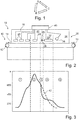
- the activated and thus recombination-active boron-oxygen correlated defects can be converted back into a recombination-inactive state by heating it to 100-200 or 100-300 ° C in the dark for a short time (see Figure 1 : Transition from active state B by annealing to inactive state A). With renewed illumination or charge carrier injection, however, the boron-oxygen correlated degradation takes place again, which is why the defects are also called metastable.
- the density of the (activated) defects depends roughly linearly on the boron concentration and roughly quadratically on the oxygen concentration in the silicon substrate.
- this effect therefore relates to boron-doped oxygen-rich silicon materials which were produced according to the Czochralski process.
- the efficiency can thereby be significantly reduced ( ⁇ 1% abs loss of efficiency). Specific degradation losses can vary depending on the architecture of the solar cell used.
- multicrystalline silicon materials with typically lower oxygen contamination show the effect, as do silicon materials in which boron is not the dominant dopant, in particular also phosphorus-doped partially compensated materials with boron admixtures.
- a first approach is to minimize the undesired oxygen contamination of the silicon crystal.
- novel coatings of the quartz crucible should prevent the same from dissolving.
- magnetic fields are mainly used in the Czochralski process, with which the convection movement of the silicon melt is suppressed directly on the quartz crucible, whereby the abrasion on the quartz crucible can be minimized.
- MCz silicon produced accordingly has correspondingly lower oxygen concentrations in the range 1 ⁇ 1017 to 5 ⁇ 1017 cm ⁇ 3.
- the manufacturing process is usually more expensive and more error-prone compared to the normal process.
- the second approach is based on reducing the boron concentration in the starting material.
- Theoretical calculations show that the efficiency potential without the restriction by boron-oxygen-correlated defects is maximal with doping around 1 ⁇ 1016 cm-3, whereas it is maximal only with lower doping if the boron-oxygen correlated degradation is taken into account.
- the maximum efficiency potential decreases with decreasing doping, so that less doped materials suffer lower degradation losses, but the maximum efficiency potential is not fully can be exploited.
- the optimal doping of the silicon substrate depends on the specific architecture of the solar cell. This approach in particular is currently being pursued by most manufacturers who use materials with boron concentrations in the range 1 ⁇ 1015 to 5 ⁇ 1015 cm-3 for oxygen-rich Cz silicon.
- the dopant boron is introduced by e.g. Replaced gallium. It could be shown that when using gallium either no corresponding defects arise or they are recombination inactive. However, in contrast to boron, gallium has a sub-optimal solubility behavior in crystal and melt, which makes it a technical challenge to produce a crystal that is homogeneously doped over the direction of crystallization. The result is greater material scrap and a higher susceptibility to errors in the process and thus higher costs. It is therefore questionable whether this approach is economically viable.
- the fourth approach takes advantage of the fact that the boron-oxygen correlated defect is not only found in an inactive one (see Figure 1 : State A) and an active state (see Figure 1 : State B) can exist, which can be converted into one another by charge carrier injection, ie degradation or heating in the dark, ie anneal, but also in a third, recombination-inactive "regenerated" state (see Figure 1 : State C), which, according to current knowledge, develops from the active state B through regeneration.
- This state is characterized in particular by the fact that (a) it has weak or negligible recombination activity and (b), in contrast to the initially present inactive state, is stable under illumination or charge carrier injection at temperatures ⁇ 150 ° C, ie there is no renewed activation of the Defects and thus degradation occurs.
- the transfer of the active defect, i.e. the state B, into the inactive third state C requires, according to current knowledge, a charge carrier injection e.g. by lighting or operating the solar cell in the forward direction at slightly increased temperatures in the range from 50 to 230 ° C, with higher temperatures or higher excess charge carrier densities accelerating the conversion of the defects.
- a charge carrier injection e.g. by lighting or operating the solar cell in the forward direction at slightly increased temperatures in the range from 50 to 230 ° C, with higher temperatures or higher excess charge carrier densities accelerating the conversion of the defects.
- the economy of the regeneration process depends essentially on the regeneration rate or the time required to bring a sufficiently large number of defects into the regenerated, advantageous state C. A process that can increase the regeneration rate and thus reduce the time required is therefore of great economic interest.
- the process step (d) corresponds precisely to the method according to this DE 10 2006 012 920 B3 .
- the method presented with the sub-steps (a) to (c) aims, among other things, at modifying a photovoltaic element in such a way that the in DE 10 2006 012 920 B3 described process optimized and thus economically attractive.
- the silicon substrate used in the method according to the invention can be a wafer which was produced according to the Czochralski method and has a boron doping in the range from 1 ⁇ 10 15 to 1 ⁇ 10 17 cm ⁇ 3.
- a wafer has a certain oxygen concentration of, for example, 1 ⁇ 1017 to 3 ⁇ 1018 cm ⁇ 3.
- other boron-doped, oxygen-containing silicon substrates can also be used, such as, for example, multicrystalline silicon wafers or silicon layers that have been deposited on a carrier from the gaseous or liquid phase.
- an emitter is formed according to the invention on the surface of the silicon substrate. This is a region which, as a rule, has a semiconductor type that is opposite to the semiconductor type of the substrate. If boron is the dominant dopant in the substrate, the substrate is p-doped. It cannot be ruled out that the semiconductor type of the substrate is n-type in spite of boron doping if corresponding amounts of n-doping substances such as phosphorus are present.
- the emitter can be formed, for example, by a superficial diffusion of dopants such as phosphorus (with p-type substrate) or boron (with n-type substrate).
- Such diffusion is typically carried out at temperatures above 800 ° C.
- other methods can also be used to produce a corresponding emitter layer.
- an emitter layer of corresponding polarity can be deposited on the substrate surface from a gaseous or liquid phase or a plasma.
- Another possibility for producing an emitter layer can be the alloying of appropriate substances.
- the surface of the silicon substrate does not have to be completely covered. It may be sufficient that only part of the surface on the front and / or back is covered with an emitter layer.
- the emitter and the substrate are of the same semiconductor type can also be implemented, e.g. if the substrate and the emitter layer have a very different band structure (heterostructures), so that a band bending occurs at the interface that results in the desired Causes potential gradient.
- a semiconductor does not even have to be used for this, since an appropriately selected metal can also lead to such band bending (MIS structures).
- Hydrogen can be introduced using a wide variety of methods.
- the hydrogen can consist of coatings applied on one or both sides such as hydrogenated silicon nitrides (a-SiNx: H), hydrogenated silicon carbides (a-SiCx: H), hydrogenated silicon oxides (a-SiOx: H), hydrogenated silicon oxynitrides (a -SiOxNy: H), hydrogenated aluminum oxides (Al2O3), hydrogenated amorphous silicon (a-Si: H) or comparable layers which can also have other functions (e.g. passivation of the surface, anti-reflective coating) are released and penetrate the silicon crystal.
- the exact parameters, in particular with regard to temperatures at which the hydrogen bound in the layer is released vary from layer to layer and are described in different embodiments. Corresponding analogous embodiments for comparable layers will be apparent to the person skilled in the art.
- this can be realized in the context of an alloying process of the metallic contacts of a solar cell, at which temperatures> 750 ° C exist for a few seconds.
- hydrogenated aluminum oxide (Al2O3) is used as the hydrogen source, which in the context of a temperature step at temperatures> 250 ° C. can release hydrogen which can penetrate the substrate.
- Al2O3 hydrogenated aluminum oxide
- the maximum temperature, temperature profile and duration must be selected accordingly in order to achieve a sufficiently high and well-distributed hydrogen concentration in the substrate.
- excess minority charge carriers are generated. This can be done, for example, by lighting or, for example, by introducing an external current.
- hydrogenated amorphous silicon (a-Si: H) is used as the hydrogen source, hydrogen being released in the context of a temperature step at temperatures> 100 ° C.
- silicon nitride layers and aluminum oxides must be selected accordingly, in order to achieve a sufficiently high and well-distributed hydrogen concentration in the substrate.
- excess minority charge carriers can be generated in the substrate during the temperature step. This can be done, for example, by lighting or, for example, by introducing an external current.
- multi-layer systems for example composed of the layers mentioned above, can also be used.
- the layer system can be designed in such a way that the layer adjacent to the substrate serves as a hydrogen source and at least one further layer is located on it.
- At least one of the further layers can act as a hydrogen diffusion barrier, ie this further layer is less permeable to hydrogen than the hydrogen-containing layer underneath and thus the hydrogen diffusion through this layer takes place only comparatively slowly as part of a high-temperature step.
- this layer serves as a hydrogen reflector and the hydrogen released from the hydrogen source is better retained in the substrate. This is advantageous because the yield of hydrogen from the source layer, ie the ratio from into the substrate diffused amount of hydrogen to released amount, in this case is better and, as mentioned later, also the out-diffusion is minimized at lower temperatures.
- the introduction of hydrogen into the substrate can also take place in other ways.
- the hydrogen can be implanted into the silicon substrate, i. protons are accelerated accordingly and shot onto or into the substrate.
- a hydrogen distribution in the substrate can be generated in a targeted manner.
- the actual ion implantation can be followed by a high temperature step> 500 ° C, which on the one hand is intended to heal any crystal damage that can occur when the protons are decelerated and, on the other hand, can also bring about a redistribution of the hydrogen.
- the introduction of the hydrogen into the substrate can also take place, for example, by diffusing atomic hydrogen from an atmosphere enriched with hydrogen or in a hydrogen-containing plasma.
- the hydrogen introduced remains in the substrate in sufficient quantity.
- the substrate reaches temperatures> 400 ° C, in particular> 450 ° C, is for a longer period, provided that no new hydrogen from the above or other sources is available, otherwise hydrogen effusion occurs to a significant extent.
- the time should be minimized in the temperature range in which the layer releases less hydrogen into the substrate than it effuses from the substrate.
- a-SiNx: H hydrogenated silicon nitride layers
- the embodiment with at least one diffusion barrier layer for hydrogen can be particularly advantageous, since the hydrogen itself is prevented from effusing from the substrate in the temperature range in question> 400 ° C or> 450 ° C. In this case, lower cooling rates greater than 0.3 K / s can still be acceptable.
- the substrate in the temperature range 230-450 ° C. for a certain period of at least 10 s, at most 30 min to hold. This can be implemented, for example, in the form of a plateau or, for example, in the form of a temperature ramp.
- the substrate is kept at a temperature in the range from 230 to 450 ° C. without generation of excess minority charge carriers, higher temperatures reducing the necessary holding time until the desired effect has been achieved.
- the substrate is then cooled down to room temperature with a steep temperature ramp.
- the substrate can then go through the regeneration process as in DE 10 2006 012 920 B3 are supplied as described.
- the substrate is kept at a temperature in the range from 230 to 450 ° C. without generation of excess minority charge carriers, with higher temperatures reducing the necessary holding time until the desired effect has been achieved.
- the substrate is transferred to the temperature range from 50 to 230 ° C, in which the regeneration process is analogous to that in DE 10 2006 012 920 B3 described can run.
- the substrate is at a temperature with generation of excess minority charge carriers, for example by lighting be kept in the range of 230..450 ° C, with higher temperatures reducing the necessary holding time until the desired effect is achieved.
- partial or complete regeneration can also occur at temperatures> 230 ° C under certain circumstances.
- the substrate is transferred to the temperature range of 50 to 230 ° C, in which the regeneration process continues if necessary, which can run faster due to the regeneration that has already taken place.
- hydrogenated silicon nitride is used as the hydrogen source, the layer being applied to a silicon wafer only on one side, while the opposite side is covered over the entire area by aluminum.
- silicon nitride layer which also functions as an anti-reflection coating and passivation layer, there is a metallic paste applied locally, for example by means of screen printing, which attacks the silicon nitride layer at high temperatures and thus makes contact with the silicon below.
- the release of the hydrogen from the silicon nitride layer takes place within the framework of a typical alloying process of metallization of the photovoltaic element, which typically takes place above 750 ° C. in a belt furnace.
- a device in the form of a specially designed continuous furnace 10 is shown, which can be used for treating a silicon substrate in the context of the production of a solar cell and which is designed to carry out an embodiment of the production method described herein and in particular the stabilization treatment step to be carried out.
- the conveyor furnace 10 has a belt 14 that can be moved by driven rollers 12. At an inlet side 16, silicon substrates can be placed on the belt 14 and then be driven by means of the belt 14 through differently heated zones of the continuous furnace 10.
- the silicon substrates can previously have been provided with a hydrogen-containing layer on their surface.
- a pattern of metal-containing paste can have been printed onto this hydrogen-containing layer, whereby the metal contacts for the solar cell are ultimately to be formed.
- One or more radiant heaters 20 are arranged in a preheating zone 18, with the aid of which the silicon substrates transported on the belt 14 can be preheated to temperatures of up to above 500.degree.
- At least one further radiant heater 24 is provided, with the aid of which silicon substrates passing through can be briefly heated to temperatures of up to above 700 ° C.
- cooling zone 26 This is followed by a cooling zone 26.
- this cooling zone 26 not only is preferably no radiant heater provided, but a cooling device 28 is even provided, with the aid of which the silicon substrates passing through can be actively cooled.
- the cooling device can be designed, for example, as a fan for blowing cool nitrogen gas into the cooling zone 26.
- a temperature holding zone 30 can then follow.
- a further radiant heater 32 is provided in this temperature holding zone 30, with the aid of which the temperature of the silicon substrates can be kept within the temperature holding zone 30 in a range from 230 ° C. to 450 ° C.
- a length of the temperature holding zone 30 can be dimensioned such that, at a given throughput speed, a silicon substrate transported by the belt 14 needs at least about 10 seconds to be transported through the temperature holding zone 30, with the aid of the radiant heater 32 at a desired temperature within the Temperature range from 230 to 450 ° C is held.
- the temperature holding zone 30 can for example be at least as long, preferably at least three times, preferably at least six times longer than the maximum heating zone 22.
- the entire continuous furnace can, for example, be more than twice as long as a conventional continuous furnace without a temperature holding zone 30.
- a strong light source 36 for example in the form of a laser with a widened laser beam or in the form of a strong lamp with wavelengths that can be absorbed by the silicon substrate, can be provided to illuminate the silicon substrates passing through with exposure intensities of at least 0.3 kW / m2 to illuminate. Since the silicon substrates are still at a temperature well above 90 ° C., at least at the beginning of the cooling zone 34, this can bring about the regeneration process and the efficiency of the solar cells ultimately produced can be stabilized.
- a light source can also be provided in the temperature holding zone 30 (in the case of the in Fig. 2 shown embodiment not provided).
- a light source can also be provided in the temperature holding zone 30 (in the case of the in Fig. 2 shown embodiment not provided).
- suitable lighting of the silicon substrates already in the temperature holding zone 30 it can possibly be supported that hydrogen which has penetrated into the silicon substrates assumes a state that is advantageous for a subsequent regeneration.
- regeneration within the silicon substrates can be carried out at least partially or, if the process is carried out appropriately, also completely, by means of suitable lighting already within the temperature holding zone 30.
- All of the described components of the continuous furnace 10 can preferably be controlled by a common controller 40.
- the silicon substrates After the silicon substrates have passed through the entire continuous furnace 10, they can be removed from an outlet side 38 and subjected to further processing or characterization steps.
- the wafer serving as silicon substrate When entering the belt furnace and passing through the preheating zone 18 (zone 1), the wafer serving as silicon substrate is first heated up to around 650 ° C, hydrogen is released from the hydrogenated silicon nitride layer previously deposited on it and the diffusion into the wafer begins (zone 2). After reaching the maximum temperature in the maximum heating zone 22, the release of hydrogen from the silicon nitride layer decreases again. At the same time, some of the hydrogen that has diffused into the wafer is already effusing again. If the temperature falls below about 650 ° C., the effusion from the wafer outweighs the release of hydrogen from the silicon nitride layer or the diffusion into the wafer and the hydrogen content of the wafer decreases again.
- the wafer is cooled down in the cooling zone 26 (zone 3) with a steep temperature ramp at a high cooling rate of, for example, more than 20 K / s and further hydrogen effusion is suppressed.
- the wafer is held in the temperature range of 230 to 450 ° C and, according to the method described, the process starts which increases the regeneration rate, which is shown in a later regeneration process step.
- the regeneration time required later can be shortened by a generation of excess charge carriers, for example by lighting in zone 4.
- a typical temperature profile when passing through a conventional continuous furnace is also shown as a dashed line 42. It can be seen that the silicon substrates cool continuously and approximately linearly after reaching a maximum temperature.
- a dwell time within the temperature range of above 450 ° C is significantly longer than in the continuous furnace according to the invention, whereas a dwell time within the temperature range of between 230 ° C and 450 ° C is significantly shorter than in the continuous furnace according to the invention.
- the inventors assume that hydrogen, in particular its amount, its bond state and charge state in the silicon crystal, have a decisive influence has the conversion of the recombination-active defects into the third, regenerated state (state C), for example through the addition of hydrogen to the defect. Since there is usually no or too little hydrogen in the silicon crystal immediately after the crystal growth, hydrogen must first be introduced into the crystal in order to enable a conversion into the regenerated state.
- various hydrogen sources can be used, as described above.
- the inventors assume that the origin of the hydrogen is of minor importance in the context of this model, as long as there is a sufficiently high concentration in the crystal of the silicon substrate in the temperature range below about 450 ° C and a sufficiently homogeneous distribution laterally and in depth . Above about 400 or 450 ° C, hydrogen can still escape to a significant extent from the silicon crystal into the environment.
- the described manufacturing process according to the invention takes this into account in that the solar cell in the manufacturing process is only as briefly as possible in a temperature range> 400 or> 450 ° C, in which the hydrogen diffuses out, but not new hydrogen e.g. is delivered from one shift.
- the bond state or charge state of the hydrogen is of decisive importance. Accordingly, in the temperature range below about 500 ° C, the hydrogen could largely exist in at least two different bond states, for example in the form of H2 molecules or bonded to boron atoms as BH pairs. However, hydrogen in such a bound form would not be sufficiently mobile.
- the regeneration in this description would correspond to a detachment of the hydrogen, the subsequent diffusion in atomic form and the attachment to a boron-oxygen-correlated defect.
- the regeneration rate i.e.
- the regeneration process depends, among other things, on how easily the hydrogen can free itself from its bound state, either purely thermally supported or through a change in the state of charge.
- the described manufacturing process according to the invention can possibly ensure that hydrogen is only slightly bound (at least with charge carrier injection) in sufficient quantity and is thus available for the regeneration process.
- the mobility of atomic hydrogen after it has been split off depends on its state of charge. In p-type silicon, the hydrogen is usually positively charged and its diffusion is hindered by electrostatic interaction in the crystal lattice. If, on the other hand, the hydrogen is in a neutral state of charge, its mobility is significantly higher.
Landscapes
- Engineering & Computer Science (AREA)
- Physics & Mathematics (AREA)
- Condensed Matter Physics & Semiconductors (AREA)
- General Physics & Mathematics (AREA)
- Computer Hardware Design (AREA)
- Microelectronics & Electronic Packaging (AREA)
- Power Engineering (AREA)
- Manufacturing & Machinery (AREA)
- Electromagnetism (AREA)
- Chemical & Material Sciences (AREA)
- Mechanical Engineering (AREA)
- General Engineering & Computer Science (AREA)
- Life Sciences & Earth Sciences (AREA)
- Crystallography & Structural Chemistry (AREA)
- Sustainable Development (AREA)
- Health & Medical Sciences (AREA)
- Toxicology (AREA)
- Combustion & Propulsion (AREA)
- Photovoltaic Devices (AREA)
- Other Surface Treatments For Metallic Materials (AREA)
Claims (15)
- Procédé de fabrication d'un élément photovoltaïque avec un rendement stabilisé, présentant les étapes suivantes :la préparation d'un substrat en silicium ;la formation d'une couche émetteur au niveau d'une surface du substrat en silicium ;la formation de contacts électriques sur le substrat en silicium ;caractérisé en ce que le procédé présente en outre une étape de traitement de stabilisation, présentant :l'incorporation d'hydrogène dans le substrat en silicium, dans lequel l'hydrogène est incorporé à des températures au-dessus de 650 °C, et un refroidissement ultérieur jusqu'à 450 °C est effectué à l'aide d'une rampe avec une vitesse de refroidissement au-dessus de 550 °C d'au moins 10 K/s ; et ensuitela génération de porteurs de charge excédentaires minoritaires dans le substrat en silicium, tandis que le substrat en silicium est à une température de plus de 230 °C.
- Procédé selon la revendication 1, dans lequel l'étape de traitement de stabilisation comprend en outre une étape de maintien du substrat en silicium dans une plage de température entre 230 °C et 450 °C pour une durée d'au moins 10 s, de préférence de 30 s, après que l'hydrogène ait été introduit dans le substrat en silicium.
- Procédé selon la revendication 2, dans lequel les porteurs de charge excédentaires minoritaires sont générées dans une étape de procédé ultérieure après le maintien du substrat en silicium dans la plage de température entre 230 °C et 450 °C.
- Procédé selon la revendication 2, dans lequel les porteurs de charge excédentaires minoritaires sont générées dans une étape de procédé commune conjointement avec le maintien du substrat en silicium dans la plage de température entre 230 °C et 450 °C.
- Procédé selon l'une des revendications 1 à 4, dans lequel le refroidissement ultérieur jusqu'à 450 °C est effectué à l'aide d'une rampe avec une vitesse de refroidissement au-dessus de 550 °C d'au moins 20 K/s, plus préférentiellement d'au moins 30 K/s, plus préférentiellement encore d'au moins 60 K/s.
- Procédé selon l'une des revendications 1 à 5, dans lequel les porteurs de charge excédentaires minoritaires sont générées par une illumination avec une intensité d'illumination supérieure à 0,3 kW/m2, de préférence supérieure à 1 kW/m2, plus préférentiellement supérieure à 3 kW/m2 à l'aide de lumière avec des longueurs d'onde inférieures à 1180 nm.
- Procédé selon l'une des revendications 1 à 6, dans lequel les porteurs de charge excédentaires minoritaires sont générées à une température du substrat en silicium entre 230 °C et 450 °C, de préférence entre 230 °C et 400 °C, plus préférentiellement entre 230 °C et 350 °C et plus préférentiellement encore entre 230 °C et 300 °C.
- Procédé selon l'une des revendications 1 à 7, présentant en outre une précipitation d'une couche contenant de l'hydrogène sur au moins une surface du substrat en silicium, laquelle sert de source d'hydrogène lors de l'incorporation d'hydrogène dans le substrat en silicium.
- Procédé selon la revendication 8, dans lequel la couche contenant de l'hydrogène est une couche de nitrure de silicium hydrogénée.
- Procédé selon la revendication 8 ou la revendication 9, dans lequel la couche contenant de l'hydrogène est recouverte au moins d'une couche qui est moins perméable à l'hydrogène que la couche contenant de l'hydrogène.
- Procédé selon l'une des revendications 1 à 10, dans lequel le substrat en silicium est revêtu d'une couche contenant de l'hydrogène et le substrat en silicium est ensuite passé dans un four continu à travers des zones thermostatées de manière appropriée.
- Dispositif de traitement d'un substrat en silicium dans le cadre d'une fabrication d'un élément photovoltaique, ledit dispositif étant sous forme d'un four continu (10), pour exécuter l'étape de traitement de stabilisation d'un procédé selon l'une des revendications 1 à 11,
ledit dispositif étant conçu avec une multiplicité de zones thermostatées de manière différente (1, 2, 3, 4, 5; 18, 22, 26, 30, 34) et présentant un dispositif d'éclairage (36), les zones pouvant être thermostatées de telle manière et le dispositif, y compris le dispositif d'éclairage, étant conçu de telle manière, qu'un substrat en silicium traversant le four continu est chauffé dans une zone de chauffage maximale (22), tout d'abord pendant un temps très court à une température au-dessus de 650 °C, puis est refroidi dans une zone de refroidissement (26) avec une vitesse de refroidissement au-dessus de 550 °C d'au moins 10 K/s jusqu'à une température en-dessous de 450 °C, et ensuite, est maintenu dans une zone de maintien de la température (30) à une température entre 230 °C et 450 °C et le substrat de silicium est simultanément ou ultérieurement éclairé à une température au-dessus de 230 °C avec une intensité d'illumination supérieure à 0,3 kW/m2. - Dispositif selon la revendication 12, dans lequel la zone de maintien de la température (30) est conçue de telle manière que le substrat en silicium est maintenu pendant au moins 10 s à une température entre 230 °C et 450 °C.
- Dispositif selon l'une des revendications 12 et 13, présentant en outre un dispositif de refroidissement (28) pour le refroidissement actif du substrat en silicium dans la zone de refroidissement (26).
- Dispositif selon la revendication 14, ledit dispositif de refroidissement présentant un ventilateur permettant l'apport de gaz de refroidissement dans la zone de refroidissement (26).
Applications Claiming Priority (2)
| Application Number | Priority Date | Filing Date | Title |
|---|---|---|---|
| DE102013010575 | 2013-06-26 | ||
| PCT/EP2013/070104 WO2014206504A1 (fr) | 2013-06-26 | 2013-09-26 | Procédé et dispositif permettant de produire un élément photovoltaïque présentant un rendement stabilisé |
Publications (2)
| Publication Number | Publication Date |
|---|---|
| EP3014663A1 EP3014663A1 (fr) | 2016-05-04 |
| EP3014663B1 true EP3014663B1 (fr) | 2020-09-02 |
Family
ID=49274634
Family Applications (1)
| Application Number | Title | Priority Date | Filing Date |
|---|---|---|---|
| EP13770893.9A Active EP3014663B1 (fr) | 2013-06-26 | 2013-09-26 | Procédé et dispositif permettant de produire un élément photovoltaïque présentant un rendement stabilisé |
Country Status (10)
| Country | Link |
|---|---|
| US (2) | US10892376B2 (fr) |
| EP (1) | EP3014663B1 (fr) |
| JP (1) | JP6266768B2 (fr) |
| KR (1) | KR101807381B1 (fr) |
| CN (1) | CN105340085B (fr) |
| DE (2) | DE112013005591C5 (fr) |
| ES (1) | ES2830766T3 (fr) |
| MY (1) | MY182430A (fr) |
| SG (1) | SG11201510423YA (fr) |
| WO (1) | WO2014206504A1 (fr) |
Families Citing this family (23)
| Publication number | Priority date | Publication date | Assignee | Title |
|---|---|---|---|---|
| DE102013113108B4 (de) | 2013-11-27 | 2024-08-29 | Hanwha Q Cells Gmbh | Solarzellenherstellungsverfahren |
| DE102013113123B4 (de) | 2013-11-27 | 2021-11-18 | Hanwha Q Cells Gmbh | Solarzellenherstellungsverfahren |
| US20160005915A1 (en) * | 2014-07-03 | 2016-01-07 | Sino-American Silicon Products Inc. | Method and apparatus for inhibiting light-induced degradation of photovoltaic device |
| JPWO2016067516A1 (ja) * | 2014-10-27 | 2017-08-10 | パナソニックIpマネジメント株式会社 | 太陽電池モジュールの製造方法、及び太陽電池モジュールの製造装置 |
| WO2016145482A1 (fr) * | 2015-03-13 | 2016-09-22 | Newsouth Innovations Pty Limited | Procédé pour le traitement de matériau de silicium |
| US10443941B2 (en) * | 2015-05-20 | 2019-10-15 | Illinois Tool Works Inc. | Light annealing in a cooling chamber of a firing furnace |
| DE102015114240A1 (de) * | 2015-08-27 | 2017-03-02 | Fraunhofer-Gesellschaft zur Förderung der angewandten Forschung e.V. | Vorrichtung und Verfahren zur Bearbeitung eines Halbleitersubstrats mittels Laserstrahlung |
| DE102015114298A1 (de) | 2015-08-27 | 2017-03-02 | Fraunhofer-Gesellschaft zur Förderung der angewandten Forschung e.V. | Verfahren und Vorrichtung zum Stabilisieren einer photovoltaischen Silizium-Solarzelle |
| DE102015219087A1 (de) * | 2015-10-02 | 2017-04-06 | Fraunhofer-Gesellschaft zur Förderung der angewandten Forschung e.V. | Verfahren zur Stabilisierung der Konversionseffizienz von Siliziumsolarzellen |
| US20190044021A1 (en) * | 2016-02-22 | 2019-02-07 | Applied Materials Italia S.R.L. | Apparatus for processing of a solar cell substrate, system for processing of a solar cell substrate and method for processing of a solar cell substrate |
| FR3051074B1 (fr) * | 2016-05-03 | 2018-05-18 | Commissariat A L'energie Atomique Et Aux Energies Alternatives | Procede de fabrication d'une cellule photovoltaique a heterojonction |
| AU2017276802A1 (en) * | 2016-06-06 | 2018-11-29 | Newsouth Innovations Pty Limited | A method for processing silicon material |
| KR20190046785A (ko) * | 2016-07-12 | 2019-05-07 | 뉴사우쓰 이노베이션스 피티와이 리미티드 | 광전 디바이스의 제조방법 |
| JP6655791B2 (ja) * | 2016-08-25 | 2020-02-26 | パナソニックIpマネジメント株式会社 | 太陽電池セル及びその製造方法 |
| TWI585988B (zh) * | 2016-10-21 | 2017-06-01 | 茂迪股份有限公司 | 太陽能電池 |
| WO2018094462A1 (fr) * | 2016-11-22 | 2018-05-31 | Newsouth Innovations Pty Limited | Passivation avancée à l'hydrogène qui évite la recombinaison induite par l'hydrogène (hir) et la détérioration de passivation de surface dans des dispositifs pv |
| KR101912772B1 (ko) * | 2016-12-26 | 2019-01-14 | 주식회사 한화 | 광기전력 소자 제조 장치 및 제조 방법 |
| US20220262973A1 (en) * | 2018-07-30 | 2022-08-18 | mPower Technology, Inc. | In-situ rapid annealing and operation of solar cells for extreme environment applications |
| DE102019102227A1 (de) | 2019-01-29 | 2019-11-14 | Universität Konstanz | Vorrichtung zum Messen einer Strahlungsintensität insbesondere in einem Durchlaufofen |
| CN112768372A (zh) * | 2019-11-05 | 2021-05-07 | 伊利诺斯工具制品有限公司 | 烧结设备 |
| DE102020002335B4 (de) | 2020-04-17 | 2022-02-24 | Ce Cell Engineering Gmbh | Verfahren zur Verbesserung des ohmschen Kontaktverhaltens zwischen einem Kontaktgitter und einer Emitterschicht einer Silizumsolarzelle |
| CN112599609B (zh) * | 2020-12-15 | 2022-07-08 | 山东力诺阳光电力科技有限公司 | 一种高效晶体硅太阳能电池及其制备方法 |
| GB202216076D0 (en) * | 2022-10-31 | 2022-12-14 | Extraterrestrial Power Pty Ltd | Solar cell |
Citations (5)
| Publication number | Priority date | Publication date | Assignee | Title |
|---|---|---|---|---|
| US20080012499A1 (en) * | 2006-06-26 | 2008-01-17 | Thermal Processing Solutions, Inc. | Rapid Thermal Firing IR Conveyor Furnace Having High Intensity Heating Section |
| DE102006012920B3 (de) * | 2006-03-21 | 2008-01-24 | Universität Konstanz | Verfahren zum Herstellen eines Photovoltaikelements mit stabilisiertem Wirkungsgrad |
| US20100267188A1 (en) * | 2009-04-16 | 2010-10-21 | Tp Solar, Inc. | Diffusion Furnaces Employing Ultra Low Mass Transport Systems and Methods of Wafer Rapid Diffusion Processing |
| FR2966980A1 (fr) * | 2010-11-02 | 2012-05-04 | Commissariat Energie Atomique | Procédé de fabrication de cellules solaires, atténuant les phénomènes de lid |
| EP2863413A2 (fr) * | 2012-05-21 | 2015-04-22 | NewSouth Innovations Pty Limited | Hydrogénation avancée de cellules solaires au silicium |
Family Cites Families (18)
| Publication number | Priority date | Publication date | Assignee | Title |
|---|---|---|---|---|
| US2949607A (en) * | 1958-09-05 | 1960-08-16 | Carl W Lamb | Multiple-band gamma matched antenna |
| DE3536299A1 (de) | 1985-10-11 | 1987-04-16 | Nukem Gmbh | Solarzelle aus silizium |
| JP4405161B2 (ja) * | 2003-02-04 | 2010-01-27 | シャープ株式会社 | 多結晶シリコン基板の処理方法、その方法により処理された多結晶シリコン基板および太陽電池 |
| JP2006073715A (ja) * | 2004-09-01 | 2006-03-16 | Sharp Corp | 太陽電池 |
| CN101478882B (zh) * | 2006-06-26 | 2013-07-10 | Tp太阳能公司 | 具有高强度加热区段的快速热烧结红外线传送带式热处理炉 |
| US7993700B2 (en) * | 2007-03-01 | 2011-08-09 | Applied Materials, Inc. | Silicon nitride passivation for a solar cell |
| JP5127273B2 (ja) * | 2007-03-27 | 2013-01-23 | 京セラ株式会社 | 太陽電池素子の製造方法 |
| WO2009052141A1 (fr) * | 2007-10-18 | 2009-04-23 | E. I. Du Pont De Nemours And Company | Compositions conductrices et procédés pour une utilisation dans la fabrication de dispositifs semi-conducteurs |
| FR2929755B1 (fr) * | 2008-04-03 | 2011-04-22 | Commissariat Energie Atomique | Procede de traitement d'un substrat semi-conducteur par activation thermique d'elements legers |
| JP5058184B2 (ja) | 2009-01-23 | 2012-10-24 | 三菱電機株式会社 | 光起電力装置の製造方法 |
| US8828776B2 (en) * | 2009-04-16 | 2014-09-09 | Tp Solar, Inc. | Diffusion furnaces employing ultra low mass transport systems and methods of wafer rapid diffusion processing |
| FR2949607B1 (fr) * | 2009-09-03 | 2011-10-21 | Commissariat Energie Atomique | Procede de traitement de cellules photovoltaiques contre la diminution du rendement lors de l'eclairement |
| WO2011050399A1 (fr) * | 2009-10-26 | 2011-05-05 | Newsouth Innovations Pty Limited | Procédé de métallisation perfectionné pour photopiles au silicium |
| US20120060758A1 (en) * | 2011-03-24 | 2012-03-15 | Primestar Solar, Inc. | Dynamic system for variable heating or cooling of linearly conveyed substrates |
| MY181635A (en) * | 2011-06-03 | 2020-12-30 | Memc Singapore Pte Ltd | Processes for suppressing minority carrier lifetime degradation in silicon wafers |
| FR2977079B1 (fr) * | 2011-06-27 | 2013-07-26 | Commissariat Energie Atomique | Procede de traitement de cellules photovoltaiques a heterojonction pour ameliorer et stabiliser leur rendement |
| US9780252B2 (en) * | 2014-10-17 | 2017-10-03 | Tp Solar, Inc. | Method and apparatus for reduction of solar cell LID |
| US11538956B2 (en) * | 2018-04-27 | 2022-12-27 | Illinois Tool Works Inc. | Methods and apparatus to control zone temperatures of a solar cell production system |
-
2013
- 2013-09-26 KR KR1020157035754A patent/KR101807381B1/ko active IP Right Grant
- 2013-09-26 SG SG11201510423YA patent/SG11201510423YA/en unknown
- 2013-09-26 JP JP2016522294A patent/JP6266768B2/ja active Active
- 2013-09-26 ES ES13770893T patent/ES2830766T3/es active Active
- 2013-09-26 WO PCT/EP2013/070104 patent/WO2014206504A1/fr active Application Filing
- 2013-09-26 CN CN201380077813.4A patent/CN105340085B/zh active Active
- 2013-09-26 US US14/900,004 patent/US10892376B2/en active Active
- 2013-09-26 DE DE112013005591.0T patent/DE112013005591C5/de active Active
- 2013-09-26 DE DE202013012849.6U patent/DE202013012849U1/de not_active Expired - Lifetime
- 2013-09-26 EP EP13770893.9A patent/EP3014663B1/fr active Active
- 2013-09-26 MY MYPI2015704636A patent/MY182430A/en unknown
-
2020
- 2020-10-22 US US17/077,995 patent/US11784279B2/en active Active
Patent Citations (5)
| Publication number | Priority date | Publication date | Assignee | Title |
|---|---|---|---|---|
| DE102006012920B3 (de) * | 2006-03-21 | 2008-01-24 | Universität Konstanz | Verfahren zum Herstellen eines Photovoltaikelements mit stabilisiertem Wirkungsgrad |
| US20080012499A1 (en) * | 2006-06-26 | 2008-01-17 | Thermal Processing Solutions, Inc. | Rapid Thermal Firing IR Conveyor Furnace Having High Intensity Heating Section |
| US20100267188A1 (en) * | 2009-04-16 | 2010-10-21 | Tp Solar, Inc. | Diffusion Furnaces Employing Ultra Low Mass Transport Systems and Methods of Wafer Rapid Diffusion Processing |
| FR2966980A1 (fr) * | 2010-11-02 | 2012-05-04 | Commissariat Energie Atomique | Procédé de fabrication de cellules solaires, atténuant les phénomènes de lid |
| EP2863413A2 (fr) * | 2012-05-21 | 2015-04-22 | NewSouth Innovations Pty Limited | Hydrogénation avancée de cellules solaires au silicium |
Also Published As
| Publication number | Publication date |
|---|---|
| KR101807381B1 (ko) | 2018-01-10 |
| DE112013005591B4 (de) | 2016-08-04 |
| DE112013005591A5 (de) | 2015-10-22 |
| SG11201510423YA (en) | 2016-01-28 |
| ES2830766T3 (es) | 2021-06-04 |
| EP3014663A1 (fr) | 2016-05-04 |
| WO2014206504A1 (fr) | 2014-12-31 |
| JP2016525276A (ja) | 2016-08-22 |
| DE112013005591C5 (de) | 2018-10-04 |
| MY182430A (en) | 2021-01-25 |
| US20160141445A1 (en) | 2016-05-19 |
| CN105340085A (zh) | 2016-02-17 |
| CN105340085B (zh) | 2018-07-06 |
| JP6266768B2 (ja) | 2018-01-24 |
| US10892376B2 (en) | 2021-01-12 |
| US11784279B2 (en) | 2023-10-10 |
| DE202013012849U1 (de) | 2020-07-03 |
| US20210057600A1 (en) | 2021-02-25 |
| KR20160023687A (ko) | 2016-03-03 |
Similar Documents
| Publication | Publication Date | Title |
|---|---|---|
| EP3014663B1 (fr) | Procédé et dispositif permettant de produire un élément photovoltaïque présentant un rendement stabilisé | |
| DE102006012920B3 (de) | Verfahren zum Herstellen eines Photovoltaikelements mit stabilisiertem Wirkungsgrad | |
| DE69827319T2 (de) | Solarzelle und Verfahren zu deren Herstellung | |
| DE69334075T2 (de) | Verbesserte rückseiten-hydrierungstechnik für fehlerpassivierung in silizium-sonnenzellen. | |
| DE102013113123B4 (de) | Solarzellenherstellungsverfahren | |
| EP1997156B1 (fr) | Procédé de fabrication d'un composant semi-conducteur avec une zone dopée superficielle ciblée au moyen de la diffusion et composant semi-conducteur correspondant | |
| DE102008055515A1 (de) | Verfahren zum Ausbilden eines Dotierstoffprofils | |
| EP3241242A1 (fr) | Dopage laser de semi-conducteurs | |
| DE102011054716A1 (de) | Gemischtes Sputtertarget aus Cadmiumsulfid und Cadmiumtellurid und Verfahren zu ihrer Verwendung | |
| DE102010006315B4 (de) | Verfahren zur lokalen Hochdotierung und Kontaktierung einer Halbleiterstruktur, welche eine Solarzelle oder eine Vorstufe einer Solarzelle ist | |
| EP3633741A1 (fr) | Procédé de fabrication d'une cellule solaire photovoltaïque doté d'une hétérojonction et d'une zone d'émetteur diffusée | |
| DE102014205350B4 (de) | Photoaktives Halbleiterbauelement sowie Verfahren zum Herstellen eines photoaktiven Halbleiterbauelementes | |
| EP3241243A1 (fr) | Procédé pour doper des semiconducteurs | |
| EP1061160A1 (fr) | Silicium à dopage structurel d'oxygène, méthode de sa préparation et son application | |
| WO2012022349A2 (fr) | Procédé de fabrication d'une cellule solaire comportant un émetteur sélectif | |
| EP1792349B1 (fr) | Procede de recristallisation et de dopage simultanes de couches semi-conductrices et systemes de couches semi-conductrices fabriques selon ledit procede | |
| DE102012207764B4 (de) | Verfahren zur Bor-Dotierung von Silizium-Wafern | |
| DE102011052916B4 (de) | Solarzellen-Herstellungsverfahren und Wafersolarzelle | |
| DE102018132244B4 (de) | Verfahren zur Herstellung von dotierten Halbleiterschichten | |
| DE102016114940B4 (de) | Thermisches Verarbeitungsverfahren für einen Wafer | |
| DE102008035846A1 (de) | Verfahren zur Herstellung von Halbleiterstrukturen auf Silizium-Germanium-Basis mit erhöhter Effizienz | |
| WO2017108592A1 (fr) | Procédé de dopage de substrats en semiconducteur au moyen d'un processus de co-diffusion et substrat en semiconducteur dopé fabriqué avec ce procédé | |
| DD256777A1 (de) | Verfahren zum erzeugen stabiler lokaler rekombinationszentren in si-halbleiterbauelementen | |
| DE102011005755A1 (de) | Verfahren zur Abscheidung eines Schichtstapels einer CIGS-Solarzelle |
Legal Events
| Date | Code | Title | Description |
|---|---|---|---|
| PUAI | Public reference made under article 153(3) epc to a published international application that has entered the european phase |
Free format text: ORIGINAL CODE: 0009012 |
|
| 17P | Request for examination filed |
Effective date: 20151222 |
|
| AK | Designated contracting states |
Kind code of ref document: A1 Designated state(s): AL AT BE BG CH CY CZ DE DK EE ES FI FR GB GR HR HU IE IS IT LI LT LU LV MC MK MT NL NO PL PT RO RS SE SI SK SM TR |
|
| AX | Request for extension of the european patent |
Extension state: BA ME |
|
| DAX | Request for extension of the european patent (deleted) | ||
| STAA | Information on the status of an ep patent application or granted ep patent |
Free format text: STATUS: EXAMINATION IS IN PROGRESS |
|
| 17Q | First examination report despatched |
Effective date: 20170828 |
|
| GRAP | Despatch of communication of intention to grant a patent |
Free format text: ORIGINAL CODE: EPIDOSNIGR1 |
|
| STAA | Information on the status of an ep patent application or granted ep patent |
Free format text: STATUS: GRANT OF PATENT IS INTENDED |
|
| RIC1 | Information provided on ipc code assigned before grant |
Ipc: F27B 9/06 20060101ALI20190208BHEP Ipc: H01L 31/068 20120101ALI20190208BHEP Ipc: H01L 31/18 20060101AFI20190208BHEP Ipc: H01L 21/67 20060101ALI20190208BHEP |
|
| INTG | Intention to grant announced |
Effective date: 20190318 |
|
| GRAJ | Information related to disapproval of communication of intention to grant by the applicant or resumption of examination proceedings by the epo deleted |
Free format text: ORIGINAL CODE: EPIDOSDIGR1 |
|
| STAA | Information on the status of an ep patent application or granted ep patent |
Free format text: STATUS: EXAMINATION IS IN PROGRESS |
|
| INTC | Intention to grant announced (deleted) | ||
| REG | Reference to a national code |
Ref country code: DE Ref legal event code: R079 Ref document number: 502013015091 Country of ref document: DE Free format text: PREVIOUS MAIN CLASS: H01L0031068000 Ipc: H01L0031180000 |
|
| GRAP | Despatch of communication of intention to grant a patent |
Free format text: ORIGINAL CODE: EPIDOSNIGR1 |
|
| STAA | Information on the status of an ep patent application or granted ep patent |
Free format text: STATUS: GRANT OF PATENT IS INTENDED |
|
| RIC1 | Information provided on ipc code assigned before grant |
Ipc: H01L 21/677 20060101ALI20200305BHEP Ipc: F27B 9/40 20060101ALI20200305BHEP Ipc: H01L 31/18 20060101AFI20200305BHEP Ipc: H01L 31/068 20120101ALI20200305BHEP Ipc: H01L 21/67 20060101ALI20200305BHEP Ipc: F27B 9/06 20060101ALI20200305BHEP |
|
| INTG | Intention to grant announced |
Effective date: 20200331 |
|
| GRAS | Grant fee paid |
Free format text: ORIGINAL CODE: EPIDOSNIGR3 |
|
| GRAA | (expected) grant |
Free format text: ORIGINAL CODE: 0009210 |
|
| STAA | Information on the status of an ep patent application or granted ep patent |
Free format text: STATUS: THE PATENT HAS BEEN GRANTED |
|
| AK | Designated contracting states |
Kind code of ref document: B1 Designated state(s): AL AT BE BG CH CY CZ DE DK EE ES FI FR GB GR HR HU IE IS IT LI LT LU LV MC MK MT NL NO PL PT RO RS SE SI SK SM TR |
|
| REG | Reference to a national code |
Ref country code: GB Ref legal event code: FG4D Free format text: NOT ENGLISH |
|
| REG | Reference to a national code |
Ref country code: AT Ref legal event code: REF Ref document number: 1309828 Country of ref document: AT Kind code of ref document: T Effective date: 20200915 Ref country code: CH Ref legal event code: EP |
|
| REG | Reference to a national code |
Ref country code: DE Ref legal event code: R096 Ref document number: 502013015091 Country of ref document: DE |
|
| REG | Reference to a national code |
Ref country code: IE Ref legal event code: FG4D Free format text: LANGUAGE OF EP DOCUMENT: GERMAN |
|
| REG | Reference to a national code |
Ref country code: NL Ref legal event code: FP |
|
| REG | Reference to a national code |
Ref country code: LT Ref legal event code: MG4D |
|
| PG25 | Lapsed in a contracting state [announced via postgrant information from national office to epo] |
Ref country code: FI Free format text: LAPSE BECAUSE OF FAILURE TO SUBMIT A TRANSLATION OF THE DESCRIPTION OR TO PAY THE FEE WITHIN THE PRESCRIBED TIME-LIMIT Effective date: 20200902 Ref country code: GR Free format text: LAPSE BECAUSE OF FAILURE TO SUBMIT A TRANSLATION OF THE DESCRIPTION OR TO PAY THE FEE WITHIN THE PRESCRIBED TIME-LIMIT Effective date: 20201203 Ref country code: NO Free format text: LAPSE BECAUSE OF FAILURE TO SUBMIT A TRANSLATION OF THE DESCRIPTION OR TO PAY THE FEE WITHIN THE PRESCRIBED TIME-LIMIT Effective date: 20201202 Ref country code: SE Free format text: LAPSE BECAUSE OF FAILURE TO SUBMIT A TRANSLATION OF THE DESCRIPTION OR TO PAY THE FEE WITHIN THE PRESCRIBED TIME-LIMIT Effective date: 20200902 Ref country code: HR Free format text: LAPSE BECAUSE OF FAILURE TO SUBMIT A TRANSLATION OF THE DESCRIPTION OR TO PAY THE FEE WITHIN THE PRESCRIBED TIME-LIMIT Effective date: 20200902 Ref country code: LT Free format text: LAPSE BECAUSE OF FAILURE TO SUBMIT A TRANSLATION OF THE DESCRIPTION OR TO PAY THE FEE WITHIN THE PRESCRIBED TIME-LIMIT Effective date: 20200902 Ref country code: BG Free format text: LAPSE BECAUSE OF FAILURE TO SUBMIT A TRANSLATION OF THE DESCRIPTION OR TO PAY THE FEE WITHIN THE PRESCRIBED TIME-LIMIT Effective date: 20201202 |
|
| PG25 | Lapsed in a contracting state [announced via postgrant information from national office to epo] |
Ref country code: PL Free format text: LAPSE BECAUSE OF FAILURE TO SUBMIT A TRANSLATION OF THE DESCRIPTION OR TO PAY THE FEE WITHIN THE PRESCRIBED TIME-LIMIT Effective date: 20200902 Ref country code: LV Free format text: LAPSE BECAUSE OF FAILURE TO SUBMIT A TRANSLATION OF THE DESCRIPTION OR TO PAY THE FEE WITHIN THE PRESCRIBED TIME-LIMIT Effective date: 20200902 Ref country code: RS Free format text: LAPSE BECAUSE OF FAILURE TO SUBMIT A TRANSLATION OF THE DESCRIPTION OR TO PAY THE FEE WITHIN THE PRESCRIBED TIME-LIMIT Effective date: 20200902 |
|
| PG25 | Lapsed in a contracting state [announced via postgrant information from national office to epo] |
Ref country code: PT Free format text: LAPSE BECAUSE OF FAILURE TO SUBMIT A TRANSLATION OF THE DESCRIPTION OR TO PAY THE FEE WITHIN THE PRESCRIBED TIME-LIMIT Effective date: 20210104 Ref country code: SM Free format text: LAPSE BECAUSE OF FAILURE TO SUBMIT A TRANSLATION OF THE DESCRIPTION OR TO PAY THE FEE WITHIN THE PRESCRIBED TIME-LIMIT Effective date: 20200902 Ref country code: RO Free format text: LAPSE BECAUSE OF FAILURE TO SUBMIT A TRANSLATION OF THE DESCRIPTION OR TO PAY THE FEE WITHIN THE PRESCRIBED TIME-LIMIT Effective date: 20200902 Ref country code: CZ Free format text: LAPSE BECAUSE OF FAILURE TO SUBMIT A TRANSLATION OF THE DESCRIPTION OR TO PAY THE FEE WITHIN THE PRESCRIBED TIME-LIMIT Effective date: 20200902 Ref country code: EE Free format text: LAPSE BECAUSE OF FAILURE TO SUBMIT A TRANSLATION OF THE DESCRIPTION OR TO PAY THE FEE WITHIN THE PRESCRIBED TIME-LIMIT Effective date: 20200902 |
|
| REG | Reference to a national code |
Ref country code: CH Ref legal event code: PL |
|
| PG25 | Lapsed in a contracting state [announced via postgrant information from national office to epo] |
Ref country code: AL Free format text: LAPSE BECAUSE OF FAILURE TO SUBMIT A TRANSLATION OF THE DESCRIPTION OR TO PAY THE FEE WITHIN THE PRESCRIBED TIME-LIMIT Effective date: 20200902 Ref country code: IS Free format text: LAPSE BECAUSE OF FAILURE TO SUBMIT A TRANSLATION OF THE DESCRIPTION OR TO PAY THE FEE WITHIN THE PRESCRIBED TIME-LIMIT Effective date: 20210102 |
|
| REG | Reference to a national code |
Ref country code: DE Ref legal event code: R097 Ref document number: 502013015091 Country of ref document: DE |
|
| REG | Reference to a national code |
Ref country code: ES Ref legal event code: FG2A Ref document number: 2830766 Country of ref document: ES Kind code of ref document: T3 Effective date: 20210604 |
|
| PG25 | Lapsed in a contracting state [announced via postgrant information from national office to epo] |
Ref country code: LU Free format text: LAPSE BECAUSE OF NON-PAYMENT OF DUE FEES Effective date: 20200926 Ref country code: SK Free format text: LAPSE BECAUSE OF FAILURE TO SUBMIT A TRANSLATION OF THE DESCRIPTION OR TO PAY THE FEE WITHIN THE PRESCRIBED TIME-LIMIT Effective date: 20200902 Ref country code: MC Free format text: LAPSE BECAUSE OF FAILURE TO SUBMIT A TRANSLATION OF THE DESCRIPTION OR TO PAY THE FEE WITHIN THE PRESCRIBED TIME-LIMIT Effective date: 20200902 |
|
| PLBE | No opposition filed within time limit |
Free format text: ORIGINAL CODE: 0009261 |
|
| STAA | Information on the status of an ep patent application or granted ep patent |
Free format text: STATUS: NO OPPOSITION FILED WITHIN TIME LIMIT |
|
| 26N | No opposition filed |
Effective date: 20210603 |
|
| GBPC | Gb: european patent ceased through non-payment of renewal fee |
Effective date: 20201202 |
|
| PG25 | Lapsed in a contracting state [announced via postgrant information from national office to epo] |
Ref country code: SI Free format text: LAPSE BECAUSE OF FAILURE TO SUBMIT A TRANSLATION OF THE DESCRIPTION OR TO PAY THE FEE WITHIN THE PRESCRIBED TIME-LIMIT Effective date: 20200902 Ref country code: IE Free format text: LAPSE BECAUSE OF NON-PAYMENT OF DUE FEES Effective date: 20200926 Ref country code: LI Free format text: LAPSE BECAUSE OF NON-PAYMENT OF DUE FEES Effective date: 20200930 Ref country code: CH Free format text: LAPSE BECAUSE OF NON-PAYMENT OF DUE FEES Effective date: 20200930 Ref country code: DK Free format text: LAPSE BECAUSE OF FAILURE TO SUBMIT A TRANSLATION OF THE DESCRIPTION OR TO PAY THE FEE WITHIN THE PRESCRIBED TIME-LIMIT Effective date: 20200902 |
|
| REG | Reference to a national code |
Ref country code: AT Ref legal event code: MM01 Ref document number: 1309828 Country of ref document: AT Kind code of ref document: T Effective date: 20200926 |
|
| PG25 | Lapsed in a contracting state [announced via postgrant information from national office to epo] |
Ref country code: GB Free format text: LAPSE BECAUSE OF NON-PAYMENT OF DUE FEES Effective date: 20201202 |
|
| PG25 | Lapsed in a contracting state [announced via postgrant information from national office to epo] |
Ref country code: AT Free format text: LAPSE BECAUSE OF NON-PAYMENT OF DUE FEES Effective date: 20200926 |
|
| PG25 | Lapsed in a contracting state [announced via postgrant information from national office to epo] |
Ref country code: IS Free format text: LAPSE BECAUSE OF FAILURE TO SUBMIT A TRANSLATION OF THE DESCRIPTION OR TO PAY THE FEE WITHIN THE PRESCRIBED TIME-LIMIT Effective date: 20210102 Ref country code: TR Free format text: LAPSE BECAUSE OF FAILURE TO SUBMIT A TRANSLATION OF THE DESCRIPTION OR TO PAY THE FEE WITHIN THE PRESCRIBED TIME-LIMIT Effective date: 20200902 Ref country code: MT Free format text: LAPSE BECAUSE OF FAILURE TO SUBMIT A TRANSLATION OF THE DESCRIPTION OR TO PAY THE FEE WITHIN THE PRESCRIBED TIME-LIMIT Effective date: 20200902 Ref country code: CY Free format text: LAPSE BECAUSE OF FAILURE TO SUBMIT A TRANSLATION OF THE DESCRIPTION OR TO PAY THE FEE WITHIN THE PRESCRIBED TIME-LIMIT Effective date: 20200902 |
|
| PG25 | Lapsed in a contracting state [announced via postgrant information from national office to epo] |
Ref country code: MK Free format text: LAPSE BECAUSE OF FAILURE TO SUBMIT A TRANSLATION OF THE DESCRIPTION OR TO PAY THE FEE WITHIN THE PRESCRIBED TIME-LIMIT Effective date: 20200902 |
|
| P01 | Opt-out of the competence of the unified patent court (upc) registered |
Effective date: 20230509 |
|
| PGFP | Annual fee paid to national office [announced via postgrant information from national office to epo] |
Ref country code: NL Payment date: 20230920 Year of fee payment: 11 |
|
| PGFP | Annual fee paid to national office [announced via postgrant information from national office to epo] |
Ref country code: FR Payment date: 20230928 Year of fee payment: 11 Ref country code: DE Payment date: 20230925 Year of fee payment: 11 Ref country code: BE Payment date: 20230920 Year of fee payment: 11 |
|
| PGFP | Annual fee paid to national office [announced via postgrant information from national office to epo] |
Ref country code: ES Payment date: 20231124 Year of fee payment: 11 |
|
| PGFP | Annual fee paid to national office [announced via postgrant information from national office to epo] |
Ref country code: IT Payment date: 20230927 Year of fee payment: 11 |