KR101807381B1 - Method and device for producing a photovoltaic element with stabilized efficiency - Google Patents
Method and device for producing a photovoltaic element with stabilized efficiency Download PDFInfo
- Publication number
- KR101807381B1 KR101807381B1 KR1020157035754A KR20157035754A KR101807381B1 KR 101807381 B1 KR101807381 B1 KR 101807381B1 KR 1020157035754 A KR1020157035754 A KR 1020157035754A KR 20157035754 A KR20157035754 A KR 20157035754A KR 101807381 B1 KR101807381 B1 KR 101807381B1
- Authority
- KR
- South Korea
- Prior art keywords
- silicon substrate
- temperature
- hydrogen
- silicon
- substrate
- Prior art date
Links
- 238000000034 method Methods 0.000 title claims abstract description 106
- 239000000758 substrate Substances 0.000 claims abstract description 192
- XUIMIQQOPSSXEZ-UHFFFAOYSA-N Silicon Chemical compound [Si] XUIMIQQOPSSXEZ-UHFFFAOYSA-N 0.000 claims abstract description 163
- 229910052710 silicon Inorganic materials 0.000 claims abstract description 162
- 239000010703 silicon Substances 0.000 claims abstract description 162
- 239000001257 hydrogen Substances 0.000 claims abstract description 149
- 229910052739 hydrogen Inorganic materials 0.000 claims abstract description 149
- UFHFLCQGNIYNRP-UHFFFAOYSA-N Hydrogen Chemical compound [H][H] UFHFLCQGNIYNRP-UHFFFAOYSA-N 0.000 claims abstract description 127
- 239000002800 charge carrier Substances 0.000 claims abstract description 49
- 238000004519 manufacturing process Methods 0.000 claims abstract description 32
- 230000006641 stabilisation Effects 0.000 claims abstract description 25
- 238000011105 stabilization Methods 0.000 claims abstract description 25
- 230000002209 hydrophobic effect Effects 0.000 claims abstract description 22
- HQVNEWCFYHHQES-UHFFFAOYSA-N silicon nitride Chemical class N12[Si]34N5[Si]62N3[Si]51N64 HQVNEWCFYHHQES-UHFFFAOYSA-N 0.000 claims abstract description 20
- 238000001816 cooling Methods 0.000 claims description 44
- 238000005286 illumination Methods 0.000 claims description 21
- 238000010438 heat treatment Methods 0.000 claims description 12
- 238000012545 processing Methods 0.000 claims description 11
- 125000004435 hydrogen atom Chemical group [H]* 0.000 claims description 5
- 238000007664 blowing Methods 0.000 claims description 4
- 230000005855 radiation Effects 0.000 claims description 4
- 238000000151 deposition Methods 0.000 claims description 3
- 239000000112 cooling gas Substances 0.000 claims description 2
- 230000000087 stabilizing effect Effects 0.000 claims description 2
- 230000035699 permeability Effects 0.000 claims 1
- 238000011069 regeneration method Methods 0.000 abstract description 51
- 230000008929 regeneration Effects 0.000 abstract description 50
- 230000008569 process Effects 0.000 abstract description 43
- 230000007547 defect Effects 0.000 description 35
- 239000000463 material Substances 0.000 description 30
- 239000013078 crystal Substances 0.000 description 29
- ZOXJGFHDIHLPTG-UHFFFAOYSA-N Boron Chemical compound [B] ZOXJGFHDIHLPTG-UHFFFAOYSA-N 0.000 description 21
- 229910052796 boron Inorganic materials 0.000 description 21
- 239000001301 oxygen Substances 0.000 description 21
- 229910052760 oxygen Inorganic materials 0.000 description 21
- QVGXLLKOCUKJST-UHFFFAOYSA-N atomic oxygen Chemical compound [O] QVGXLLKOCUKJST-UHFFFAOYSA-N 0.000 description 20
- 238000009792 diffusion process Methods 0.000 description 19
- 230000000694 effects Effects 0.000 description 16
- 150000002431 hydrogen Chemical class 0.000 description 15
- 235000012431 wafers Nutrition 0.000 description 15
- 230000015556 catabolic process Effects 0.000 description 13
- 238000006731 degradation reaction Methods 0.000 description 13
- 229910052581 Si3N4 Inorganic materials 0.000 description 10
- XGCTUKUCGUNZDN-UHFFFAOYSA-N [B].O=O Chemical compound [B].O=O XGCTUKUCGUNZDN-UHFFFAOYSA-N 0.000 description 10
- 239000004065 semiconductor Substances 0.000 description 10
- 238000002347 injection Methods 0.000 description 9
- 239000007924 injection Substances 0.000 description 9
- 238000013459 approach Methods 0.000 description 8
- 230000004888 barrier function Effects 0.000 description 8
- 239000002019 doping agent Substances 0.000 description 7
- 230000006798 recombination Effects 0.000 description 7
- 238000002231 Czochralski process Methods 0.000 description 6
- GYHNNYVSQQEPJS-UHFFFAOYSA-N Gallium Chemical compound [Ga] GYHNNYVSQQEPJS-UHFFFAOYSA-N 0.000 description 6
- 239000006096 absorbing agent Substances 0.000 description 6
- 229910052733 gallium Inorganic materials 0.000 description 6
- 239000007789 gas Substances 0.000 description 6
- 229910052751 metal Inorganic materials 0.000 description 6
- 239000002184 metal Substances 0.000 description 6
- 239000010453 quartz Substances 0.000 description 6
- 238000005215 recombination Methods 0.000 description 6
- VYPSYNLAJGMNEJ-UHFFFAOYSA-N silicon dioxide Inorganic materials O=[Si]=O VYPSYNLAJGMNEJ-UHFFFAOYSA-N 0.000 description 6
- 229910021417 amorphous silicon Inorganic materials 0.000 description 5
- 230000007704 transition Effects 0.000 description 5
- 125000004429 atom Chemical group 0.000 description 4
- 238000000576 coating method Methods 0.000 description 4
- 238000009826 distribution Methods 0.000 description 4
- 239000000155 melt Substances 0.000 description 4
- 229910021420 polycrystalline silicon Inorganic materials 0.000 description 4
- 238000000926 separation method Methods 0.000 description 4
- IJGRMHOSHXDMSA-UHFFFAOYSA-N Atomic nitrogen Chemical compound N#N IJGRMHOSHXDMSA-UHFFFAOYSA-N 0.000 description 3
- 229910004205 SiNX Inorganic materials 0.000 description 3
- 230000009286 beneficial effect Effects 0.000 description 3
- 230000008901 benefit Effects 0.000 description 3
- 230000015572 biosynthetic process Effects 0.000 description 3
- 239000011248 coating agent Substances 0.000 description 3
- 239000000356 contaminant Substances 0.000 description 3
- 229910021419 crystalline silicon Inorganic materials 0.000 description 3
- 238000010304 firing Methods 0.000 description 3
- 238000012423 maintenance Methods 0.000 description 3
- 238000002161 passivation Methods 0.000 description 3
- 239000002243 precursor Substances 0.000 description 3
- 239000002210 silicon-based material Substances 0.000 description 3
- 229910018072 Al 2 O 3 Inorganic materials 0.000 description 2
- QGZKDVFQNNGYKY-UHFFFAOYSA-N Ammonia Chemical compound N QGZKDVFQNNGYKY-UHFFFAOYSA-N 0.000 description 2
- OAICVXFJPJFONN-UHFFFAOYSA-N Phosphorus Chemical compound [P] OAICVXFJPJFONN-UHFFFAOYSA-N 0.000 description 2
- 238000005275 alloying Methods 0.000 description 2
- 239000006117 anti-reflective coating Substances 0.000 description 2
- 238000006243 chemical reaction Methods 0.000 description 2
- 238000002425 crystallisation Methods 0.000 description 2
- 230000008025 crystallization Effects 0.000 description 2
- 230000001419 dependent effect Effects 0.000 description 2
- 238000004090 dissolution Methods 0.000 description 2
- 230000002349 favourable effect Effects 0.000 description 2
- BHEPBYXIRTUNPN-UHFFFAOYSA-N hydridophosphorus(.) (triplet) Chemical compound [PH] BHEPBYXIRTUNPN-UHFFFAOYSA-N 0.000 description 2
- 239000007791 liquid phase Substances 0.000 description 2
- 230000033001 locomotion Effects 0.000 description 2
- 239000000203 mixture Substances 0.000 description 2
- 238000012986 modification Methods 0.000 description 2
- 230000004048 modification Effects 0.000 description 2
- 230000007935 neutral effect Effects 0.000 description 2
- 239000012071 phase Substances 0.000 description 2
- 229910052698 phosphorus Inorganic materials 0.000 description 2
- 239000011574 phosphorus Substances 0.000 description 2
- 238000000623 plasma-assisted chemical vapour deposition Methods 0.000 description 2
- 230000001105 regulatory effect Effects 0.000 description 2
- 238000004904 shortening Methods 0.000 description 2
- 150000003376 silicon Chemical class 0.000 description 2
- HBMJWWWQQXIZIP-UHFFFAOYSA-N silicon carbide Chemical class [Si+]#[C-] HBMJWWWQQXIZIP-UHFFFAOYSA-N 0.000 description 2
- LIVNPJMFVYWSIS-UHFFFAOYSA-N silicon monoxide Chemical class [Si-]#[O+] LIVNPJMFVYWSIS-UHFFFAOYSA-N 0.000 description 2
- 239000007858 starting material Substances 0.000 description 2
- PNEYBMLMFCGWSK-UHFFFAOYSA-N Alumina Chemical class [O-2].[O-2].[O-2].[Al+3].[Al+3] PNEYBMLMFCGWSK-UHFFFAOYSA-N 0.000 description 1
- YZCKVEUIGOORGS-UHFFFAOYSA-N Hydrogen atom Chemical compound [H] YZCKVEUIGOORGS-UHFFFAOYSA-N 0.000 description 1
- 229910004012 SiCx Inorganic materials 0.000 description 1
- 229910020286 SiOxNy Inorganic materials 0.000 description 1
- BLRPTPMANUNPDV-UHFFFAOYSA-N Silane Chemical compound [SiH4] BLRPTPMANUNPDV-UHFFFAOYSA-N 0.000 description 1
- 244000299461 Theobroma cacao Species 0.000 description 1
- LBZRRXXISSKCHV-UHFFFAOYSA-N [B].[O] Chemical class [B].[O] LBZRRXXISSKCHV-UHFFFAOYSA-N 0.000 description 1
- NCMAYWHYXSWFGB-UHFFFAOYSA-N [Si].[N+][O-] Chemical class [Si].[N+][O-] NCMAYWHYXSWFGB-UHFFFAOYSA-N 0.000 description 1
- 230000009471 action Effects 0.000 description 1
- 230000004913 activation Effects 0.000 description 1
- 229910045601 alloy Inorganic materials 0.000 description 1
- 239000000956 alloy Substances 0.000 description 1
- 229910052782 aluminium Inorganic materials 0.000 description 1
- XAGFODPZIPBFFR-UHFFFAOYSA-N aluminium Chemical compound [Al] XAGFODPZIPBFFR-UHFFFAOYSA-N 0.000 description 1
- 229910021529 ammonia Inorganic materials 0.000 description 1
- 238000000137 annealing Methods 0.000 description 1
- 230000003667 anti-reflective effect Effects 0.000 description 1
- 238000005452 bending Methods 0.000 description 1
- 229910052799 carbon Inorganic materials 0.000 description 1
- 239000000969 carrier Substances 0.000 description 1
- 230000001364 causal effect Effects 0.000 description 1
- 238000012512 characterization method Methods 0.000 description 1
- 235000019219 chocolate Nutrition 0.000 description 1
- 238000004140 cleaning Methods 0.000 description 1
- 238000003776 cleavage reaction Methods 0.000 description 1
- 230000000295 complement effect Effects 0.000 description 1
- 238000011109 contamination Methods 0.000 description 1
- 238000005336 cracking Methods 0.000 description 1
- 230000007423 decrease Effects 0.000 description 1
- 230000008021 deposition Effects 0.000 description 1
- 230000002542 deteriorative effect Effects 0.000 description 1
- 229910001873 dinitrogen Inorganic materials 0.000 description 1
- -1 e.g. Substances 0.000 description 1
- 230000005670 electromagnetic radiation Effects 0.000 description 1
- 230000009881 electrostatic interaction Effects 0.000 description 1
- 238000009472 formulation Methods 0.000 description 1
- 239000000446 fuel Substances 0.000 description 1
- 230000006870 function Effects 0.000 description 1
- 230000005484 gravity Effects 0.000 description 1
- 239000012051 hydrophobic carrier Substances 0.000 description 1
- 239000011261 inert gas Substances 0.000 description 1
- 230000005764 inhibitory process Effects 0.000 description 1
- 238000005468 ion implantation Methods 0.000 description 1
- 230000007774 longterm Effects 0.000 description 1
- 239000006166 lysate Substances 0.000 description 1
- 238000001465 metallisation Methods 0.000 description 1
- 239000013081 microcrystal Substances 0.000 description 1
- 229910021421 monocrystalline silicon Inorganic materials 0.000 description 1
- 229910052757 nitrogen Inorganic materials 0.000 description 1
- TWNQGVIAIRXVLR-UHFFFAOYSA-N oxo(oxoalumanyloxy)alumane Chemical compound O=[Al]O[Al]=O TWNQGVIAIRXVLR-UHFFFAOYSA-N 0.000 description 1
- 230000035515 penetration Effects 0.000 description 1
- 231100000289 photo-effect Toxicity 0.000 description 1
- 238000004886 process control Methods 0.000 description 1
- 230000035755 proliferation Effects 0.000 description 1
- 230000002035 prolonged effect Effects 0.000 description 1
- 230000009257 reactivity Effects 0.000 description 1
- 238000011160 research Methods 0.000 description 1
- 230000004044 response Effects 0.000 description 1
- 230000007017 scission Effects 0.000 description 1
- 238000007650 screen-printing Methods 0.000 description 1
- 230000035945 sensitivity Effects 0.000 description 1
- 229910000077 silane Inorganic materials 0.000 description 1
- 229910052814 silicon oxide Inorganic materials 0.000 description 1
- 239000000126 substance Substances 0.000 description 1
- 239000002699 waste material Substances 0.000 description 1
Images


Classifications
-
- H—ELECTRICITY
- H01—ELECTRIC ELEMENTS
- H01L—SEMICONDUCTOR DEVICES NOT COVERED BY CLASS H10
- H01L31/00—Semiconductor devices sensitive to infrared radiation, light, electromagnetic radiation of shorter wavelength or corpuscular radiation and specially adapted either for the conversion of the energy of such radiation into electrical energy or for the control of electrical energy by such radiation; Processes or apparatus specially adapted for the manufacture or treatment thereof or of parts thereof; Details thereof
- H01L31/02—Details
- H01L31/0236—Special surface textures
- H01L31/02363—Special surface textures of the semiconductor body itself, e.g. textured active layers
-
- F—MECHANICAL ENGINEERING; LIGHTING; HEATING; WEAPONS; BLASTING
- F27—FURNACES; KILNS; OVENS; RETORTS
- F27B—FURNACES, KILNS, OVENS, OR RETORTS IN GENERAL; OPEN SINTERING OR LIKE APPARATUS
- F27B9/00—Furnaces through which the charge is moved mechanically, e.g. of tunnel type; Similar furnaces in which the charge moves by gravity
- F27B9/06—Furnaces through which the charge is moved mechanically, e.g. of tunnel type; Similar furnaces in which the charge moves by gravity heated without contact between combustion gases and charge; electrically heated
- F27B9/062—Furnaces through which the charge is moved mechanically, e.g. of tunnel type; Similar furnaces in which the charge moves by gravity heated without contact between combustion gases and charge; electrically heated electrically heated
- F27B9/066—Furnaces through which the charge is moved mechanically, e.g. of tunnel type; Similar furnaces in which the charge moves by gravity heated without contact between combustion gases and charge; electrically heated electrically heated heated by lamps
-
- F—MECHANICAL ENGINEERING; LIGHTING; HEATING; WEAPONS; BLASTING
- F27—FURNACES; KILNS; OVENS; RETORTS
- F27B—FURNACES, KILNS, OVENS, OR RETORTS IN GENERAL; OPEN SINTERING OR LIKE APPARATUS
- F27B9/00—Furnaces through which the charge is moved mechanically, e.g. of tunnel type; Similar furnaces in which the charge moves by gravity
- F27B9/30—Details, accessories, or equipment peculiar to furnaces of these types
- F27B9/40—Arrangements of controlling or monitoring devices
-
- H—ELECTRICITY
- H01—ELECTRIC ELEMENTS
- H01L—SEMICONDUCTOR DEVICES NOT COVERED BY CLASS H10
- H01L21/00—Processes or apparatus adapted for the manufacture or treatment of semiconductor or solid state devices or of parts thereof
- H01L21/67—Apparatus specially adapted for handling semiconductor or electric solid state devices during manufacture or treatment thereof; Apparatus specially adapted for handling wafers during manufacture or treatment of semiconductor or electric solid state devices or components ; Apparatus not specifically provided for elsewhere
- H01L21/67005—Apparatus not specifically provided for elsewhere
- H01L21/67011—Apparatus for manufacture or treatment
- H01L21/67098—Apparatus for thermal treatment
- H01L21/67109—Apparatus for thermal treatment mainly by convection
-
- H—ELECTRICITY
- H01—ELECTRIC ELEMENTS
- H01L—SEMICONDUCTOR DEVICES NOT COVERED BY CLASS H10
- H01L21/00—Processes or apparatus adapted for the manufacture or treatment of semiconductor or solid state devices or of parts thereof
- H01L21/67—Apparatus specially adapted for handling semiconductor or electric solid state devices during manufacture or treatment thereof; Apparatus specially adapted for handling wafers during manufacture or treatment of semiconductor or electric solid state devices or components ; Apparatus not specifically provided for elsewhere
- H01L21/67005—Apparatus not specifically provided for elsewhere
- H01L21/67011—Apparatus for manufacture or treatment
- H01L21/67098—Apparatus for thermal treatment
- H01L21/67115—Apparatus for thermal treatment mainly by radiation
-
- H—ELECTRICITY
- H01—ELECTRIC ELEMENTS
- H01L—SEMICONDUCTOR DEVICES NOT COVERED BY CLASS H10
- H01L21/00—Processes or apparatus adapted for the manufacture or treatment of semiconductor or solid state devices or of parts thereof
- H01L21/67—Apparatus specially adapted for handling semiconductor or electric solid state devices during manufacture or treatment thereof; Apparatus specially adapted for handling wafers during manufacture or treatment of semiconductor or electric solid state devices or components ; Apparatus not specifically provided for elsewhere
- H01L21/67005—Apparatus not specifically provided for elsewhere
- H01L21/67242—Apparatus for monitoring, sorting or marking
- H01L21/67248—Temperature monitoring
-
- H—ELECTRICITY
- H01—ELECTRIC ELEMENTS
- H01L—SEMICONDUCTOR DEVICES NOT COVERED BY CLASS H10
- H01L21/00—Processes or apparatus adapted for the manufacture or treatment of semiconductor or solid state devices or of parts thereof
- H01L21/67—Apparatus specially adapted for handling semiconductor or electric solid state devices during manufacture or treatment thereof; Apparatus specially adapted for handling wafers during manufacture or treatment of semiconductor or electric solid state devices or components ; Apparatus not specifically provided for elsewhere
- H01L21/677—Apparatus specially adapted for handling semiconductor or electric solid state devices during manufacture or treatment thereof; Apparatus specially adapted for handling wafers during manufacture or treatment of semiconductor or electric solid state devices or components ; Apparatus not specifically provided for elsewhere for conveying, e.g. between different workstations
- H01L21/67739—Apparatus specially adapted for handling semiconductor or electric solid state devices during manufacture or treatment thereof; Apparatus specially adapted for handling wafers during manufacture or treatment of semiconductor or electric solid state devices or components ; Apparatus not specifically provided for elsewhere for conveying, e.g. between different workstations into and out of processing chamber
- H01L21/6776—Continuous loading and unloading into and out of a processing chamber, e.g. transporting belts within processing chambers
-
- H—ELECTRICITY
- H01—ELECTRIC ELEMENTS
- H01L—SEMICONDUCTOR DEVICES NOT COVERED BY CLASS H10
- H01L31/00—Semiconductor devices sensitive to infrared radiation, light, electromagnetic radiation of shorter wavelength or corpuscular radiation and specially adapted either for the conversion of the energy of such radiation into electrical energy or for the control of electrical energy by such radiation; Processes or apparatus specially adapted for the manufacture or treatment thereof or of parts thereof; Details thereof
- H01L31/04—Semiconductor devices sensitive to infrared radiation, light, electromagnetic radiation of shorter wavelength or corpuscular radiation and specially adapted either for the conversion of the energy of such radiation into electrical energy or for the control of electrical energy by such radiation; Processes or apparatus specially adapted for the manufacture or treatment thereof or of parts thereof; Details thereof adapted as photovoltaic [PV] conversion devices
- H01L31/06—Semiconductor devices sensitive to infrared radiation, light, electromagnetic radiation of shorter wavelength or corpuscular radiation and specially adapted either for the conversion of the energy of such radiation into electrical energy or for the control of electrical energy by such radiation; Processes or apparatus specially adapted for the manufacture or treatment thereof or of parts thereof; Details thereof adapted as photovoltaic [PV] conversion devices characterised by at least one potential-jump barrier or surface barrier
- H01L31/068—Semiconductor devices sensitive to infrared radiation, light, electromagnetic radiation of shorter wavelength or corpuscular radiation and specially adapted either for the conversion of the energy of such radiation into electrical energy or for the control of electrical energy by such radiation; Processes or apparatus specially adapted for the manufacture or treatment thereof or of parts thereof; Details thereof adapted as photovoltaic [PV] conversion devices characterised by at least one potential-jump barrier or surface barrier the potential barriers being only of the PN homojunction type, e.g. bulk silicon PN homojunction solar cells or thin film polycrystalline silicon PN homojunction solar cells
-
- H—ELECTRICITY
- H01—ELECTRIC ELEMENTS
- H01L—SEMICONDUCTOR DEVICES NOT COVERED BY CLASS H10
- H01L31/00—Semiconductor devices sensitive to infrared radiation, light, electromagnetic radiation of shorter wavelength or corpuscular radiation and specially adapted either for the conversion of the energy of such radiation into electrical energy or for the control of electrical energy by such radiation; Processes or apparatus specially adapted for the manufacture or treatment thereof or of parts thereof; Details thereof
- H01L31/18—Processes or apparatus specially adapted for the manufacture or treatment of these devices or of parts thereof
- H01L31/1804—Processes or apparatus specially adapted for the manufacture or treatment of these devices or of parts thereof comprising only elements of Group IV of the Periodic System
-
- H—ELECTRICITY
- H01—ELECTRIC ELEMENTS
- H01L—SEMICONDUCTOR DEVICES NOT COVERED BY CLASS H10
- H01L31/00—Semiconductor devices sensitive to infrared radiation, light, electromagnetic radiation of shorter wavelength or corpuscular radiation and specially adapted either for the conversion of the energy of such radiation into electrical energy or for the control of electrical energy by such radiation; Processes or apparatus specially adapted for the manufacture or treatment thereof or of parts thereof; Details thereof
- H01L31/18—Processes or apparatus specially adapted for the manufacture or treatment of these devices or of parts thereof
- H01L31/186—Particular post-treatment for the devices, e.g. annealing, impurity gettering, short-circuit elimination, recrystallisation
- H01L31/1864—Annealing
-
- H—ELECTRICITY
- H01—ELECTRIC ELEMENTS
- H01L—SEMICONDUCTOR DEVICES NOT COVERED BY CLASS H10
- H01L31/00—Semiconductor devices sensitive to infrared radiation, light, electromagnetic radiation of shorter wavelength or corpuscular radiation and specially adapted either for the conversion of the energy of such radiation into electrical energy or for the control of electrical energy by such radiation; Processes or apparatus specially adapted for the manufacture or treatment thereof or of parts thereof; Details thereof
- H01L31/18—Processes or apparatus specially adapted for the manufacture or treatment of these devices or of parts thereof
- H01L31/186—Particular post-treatment for the devices, e.g. annealing, impurity gettering, short-circuit elimination, recrystallisation
- H01L31/1868—Passivation
-
- Y—GENERAL TAGGING OF NEW TECHNOLOGICAL DEVELOPMENTS; GENERAL TAGGING OF CROSS-SECTIONAL TECHNOLOGIES SPANNING OVER SEVERAL SECTIONS OF THE IPC; TECHNICAL SUBJECTS COVERED BY FORMER USPC CROSS-REFERENCE ART COLLECTIONS [XRACs] AND DIGESTS
- Y02—TECHNOLOGIES OR APPLICATIONS FOR MITIGATION OR ADAPTATION AGAINST CLIMATE CHANGE
- Y02E—REDUCTION OF GREENHOUSE GAS [GHG] EMISSIONS, RELATED TO ENERGY GENERATION, TRANSMISSION OR DISTRIBUTION
- Y02E10/00—Energy generation through renewable energy sources
- Y02E10/50—Photovoltaic [PV] energy
- Y02E10/546—Polycrystalline silicon PV cells
-
- Y—GENERAL TAGGING OF NEW TECHNOLOGICAL DEVELOPMENTS; GENERAL TAGGING OF CROSS-SECTIONAL TECHNOLOGIES SPANNING OVER SEVERAL SECTIONS OF THE IPC; TECHNICAL SUBJECTS COVERED BY FORMER USPC CROSS-REFERENCE ART COLLECTIONS [XRACs] AND DIGESTS
- Y02—TECHNOLOGIES OR APPLICATIONS FOR MITIGATION OR ADAPTATION AGAINST CLIMATE CHANGE
- Y02E—REDUCTION OF GREENHOUSE GAS [GHG] EMISSIONS, RELATED TO ENERGY GENERATION, TRANSMISSION OR DISTRIBUTION
- Y02E10/00—Energy generation through renewable energy sources
- Y02E10/50—Photovoltaic [PV] energy
- Y02E10/547—Monocrystalline silicon PV cells
-
- Y—GENERAL TAGGING OF NEW TECHNOLOGICAL DEVELOPMENTS; GENERAL TAGGING OF CROSS-SECTIONAL TECHNOLOGIES SPANNING OVER SEVERAL SECTIONS OF THE IPC; TECHNICAL SUBJECTS COVERED BY FORMER USPC CROSS-REFERENCE ART COLLECTIONS [XRACs] AND DIGESTS
- Y02—TECHNOLOGIES OR APPLICATIONS FOR MITIGATION OR ADAPTATION AGAINST CLIMATE CHANGE
- Y02P—CLIMATE CHANGE MITIGATION TECHNOLOGIES IN THE PRODUCTION OR PROCESSING OF GOODS
- Y02P70/00—Climate change mitigation technologies in the production process for final industrial or consumer products
- Y02P70/50—Manufacturing or production processes characterised by the final manufactured product
-
- Y02P70/521—
Abstract
안정화된 효율을 가지는 광기전력 소자를 생산하기 위한 방법, 및 예를 들어, 특별히 개조된 연속로의 형태에서, 상기 방법을 수행하기 위해 사용될 수도 있는 디바이스가 제공된다. 에미터 층 및 전기 접촉이 제공되는 실리콘 기판은, 그렇게 함으로써, 안정화 처리 단계를 받는다. 그러한 단계에서, 예를 들어, 수소화된 질화 실리콘 층으로부터의 수소는, 예를 들어, 최대 온도의 영역(2) 내의 상기 실리콘 기판으로 도입된다. 그 다음에, 상기 실리콘 기판은, 수소 유출을 피하기 위해, 목적으로 영역(3)에서 빠르게 냉각될 수도 있다. 그 다음에, 상기 실리콘 기판은, 예를 들어, 적어도 10 초의 기간 동안, 230 ℃ 내지 450 ℃의 온도 범위 내에, 예를 들어, 영역(4)에서 목적으로 유지될 수도 있다. 상기 이전에 도입된 수소는, 그렇게 함으로써 유리한 결합 상태를 추정할 수도 있다. 동시에 또는 그 후에, 재생은, 적어도 90 ℃, 바람직하게는 적어도 230 ℃의 온도에서 상기 기판에서의 과잉 소수 전하 캐리어를 발생시킴으로써 수행될 수도 있다. 전체적으로, 제안된 방법과 함께, 광기전력 소자의 생산에서 재생 공정은, 이는 예를 들어, 적합하게 변형된 연속로에서 수행될 수도 있도록 현저하게 가속화될 수도 있다.There is provided a method for producing a photovoltaic device having a stabilized efficiency, and a device that may be used for carrying out the method, for example, in the form of a specially modified continuous furnace. The emitter layer and the silicon substrate provided with electrical contact are thereby subjected to a stabilization treatment step. At that stage, for example, hydrogen from the hydrogenated silicon nitride layer is introduced into the silicon substrate, for example, in the region 2 of maximum temperature. The silicon substrate may then be rapidly cooled in region 3 for the purpose, to avoid hydrogen spillage. The silicon substrate may then be held within a temperature range of 230 ° C to 450 ° C, for example, in region 4 for a period of at least 10 seconds, for example. The previously introduced hydrogen may thereby estimate an advantageous bonding state. At the same time or thereafter, regeneration may be carried out by generating excess hydrophobic charge carriers in the substrate at a temperature of at least 90 캜, preferably at least 230 캜. Overall, in conjunction with the proposed method, the regeneration process in the production of photovoltaic devices may be significantly accelerated, for example, to be performed in a suitably modified continuous furnace, for example.
Description
본 발명의 분야Field of the Invention
본 발명은, 안정화 처리 단계에 의한 광기전력 소자(photovoltaic element)를 생산하기 위한 방법에 관한 것으로서, 상기 광기전력 소자의 효율은 안정화 처리 단계에 의해 안정화된다. 특히, 본 발명은, 붕소-도핑된, 산소-함유하는 실리콘 기판에 기초한 태양 전지를 생산하기 위한 방법에 관한 것이다. 본 발명은 추가적으로, 광기전력 소자의 생산의 내용 내의 실리콘 기판을 처리하기 위한 디바이스에 관한 것으로서, 상기 디바이스는, 본 발명에 따른 방법의 안정화 처리 단계를 실행하기 위해 설정된 것이다. The present invention relates to a method for producing a photovoltaic element by a stabilization step, wherein the efficiency of the photovoltaic element is stabilized by a stabilization processing step. In particular, the present invention relates to a method for producing a solar cell based on a boron-doped, oxygen-containing silicon substrate. The invention further relates to a device for processing a silicon substrate in the context of the production of a photovoltaic device, said device being set for carrying out the stabilization step of the method according to the invention.
기술적인 배경Technical background
광기전력 소자로서 태양 전지는, 빛을 전류로 전환시키기 위한 역할을 한다. 예를 들어, 에미터 영역(emitter region)과 베이스 영역(base region) 사이의 pn 접합에서 공간적으로 분리된, 빛-발생된 전하 운반체 쌍은, 상기 태양 전지의 전기 접점의 도움으로 외부의 전류 회로로 공급되어야 한다. 전기 접점 배열은, 상기 태양 전지의 상기 에미터와 상기 베이스 둘 다에서 그러한 목적을 위해 제공되어야 한다. As photovoltaic devices, solar cells serve to convert light into current. For example, a pair of light-generated charge carriers, spatially separated from the pn junction between the emitter region and the base region, is coupled to the external current circuit < RTI ID = 0.0 >Lt; / RTI > An electrical contact arrangement should be provided for that purpose in both the emitter of the solar cell and the base.
태양 전지는 오늘날, 주로 반도체 기판 물질로서 실리콘을 기초로 제조되고 있다. 실리콘 기판은 그렇게 함으로써 단결정 또는 다결정 웨이퍼의 형태로 자주 제공된다. 결정질 실리콘 웨이퍼를 기초로 생산된 태양 전지의 경우에, 시간에 따라(over time) 상기 태양 전지의 효율을 감소시키는 열화 효과(degradation effect)가 발생할 수도 있음을 여러 번 관찰되고 있다. 1 % 이상의 현저한 효율 손실이 관찰되고 있다. Solar cells are now being manufactured on silicon as the predominantly semiconductor substrate material. The silicon substrate is thus frequently provided in the form of a single crystal or polycrystalline wafer. It has been observed several times that in the case of a solar cell produced on the basis of a crystalline silicon wafer, a degradation effect which reduces the efficiency of the solar cell over time may occur. A remarkable efficiency loss of more than 1% is observed.
DE 10 2006 012 920 A1은, 안정화된 효율을 가지는 광기전력 소자를 제조하기 위한 방법을 개시하고 있다. 본원에 기재된 발명은, 본 출원으로서 동일한 발명자와 적어도 부분적으로 속한다. 광기전력 소자의 효율이 안정화될 수도 있고, 다시 말해서, 광기전력 소자의 효율이, 상기 광기전력 소자가 충분하게 긴 기간 동안에 상승된 온도 범위 내에 유지되고, 동시에, 과량의 소수 전하 캐리어가, 예를 들어, 조명 또는 전기 전압(electric voltage)의 적용에 의해 상기 실리콘 기판에 발생되는, 안정화 처리 단계를 상기 광기전력 소자에서 실행됨으로써 저하가 예방될 수도 있음을 그 때에 인식하였다. DE 10 2006 012 920 A1 discloses a method for manufacturing a photovoltaic device with stabilized efficiency. The invention described herein pertains, at least in part, to the same inventor as the present application. The efficiency of the photovoltaic element may be stabilized, in other words, the efficiency of the photovoltaic element may be such that the photovoltaic element is maintained within the elevated temperature range for a sufficiently long period of time, and at the same time, For that reason, it has been recognized at this time that the stabilization treatment step, which is generated in the silicon substrate by the application of illumination or an electric voltage, may be prevented from deteriorating by being implemented in the photovoltaic device.
그러나, 실리콘 기판이 안정화 처리 단계를 받아야 하는 공정 기간이, 효율의 충분한 안정화를 달성하기 위해, 비교적 길어질 것으로 지금까지 추정되고 있다. 특히 자동화된 산업 제조 라인의 경우에, 이는 지연 및 그 결과로서 병목현상(bottleneck)의 형성을 유도할 수도 있다. However, the process period in which the silicon substrate is subjected to the stabilization process step has been estimated so far to be relatively long in order to achieve sufficient stabilization of the efficiency. Especially in the case of automated industrial manufacturing lines, this may lead to delay and consequent bottleneck formation.
본 발명의 요약SUMMARY OF THE INVENTION
안정화된 효율을 가지는 광기전력 소자를 생산하기 위한 개선된 방법의 필요성이 있을 수 있다. 특히, 효율이 짧은 공정 시간 내에 안정화되는 것을 가능하게 하는 이러한 방법에 대한 필요성이 있을 수 있다. 게다가, 특히 기재된 방법의 안정화 처리 단계를 수행하는 것을 가능하게 하는 광기전력 소자의 생산의 상황 내에 실리콘 기판을 처리하기 위한 디바이스에 대한 필요성이 있을 수 있다(there may be a need for a device for treating a silicon substrate within the context of a production of a photovoltaic element which in particular allows the stabilisation treatment step of the described method to be carried out). There may be a need for an improved method for producing a photovoltaic device with stabilized efficiency. In particular, there may be a need for such a method that enables efficiency to be stabilized within short process times. In addition, there may be a need for a device for processing a silicon substrate within the context of the production of photovoltaic devices, which makes it possible, in particular, to carry out the stabilization step of the process described (for example, Silicon substrates have been found to have a photovoltaic element, which allows the stabilization treatment to be carried out.
이러한 필요성은 독립된 청구항에 따른 방법 및 디바이스에 충족될 수도 있다. 본 발명의 실시형태는, 종속항 및 하기의 기재에 기재되어 있다. This need may be met by methods and devices according to the independent claims. Embodiments of the present invention are described in the dependent claims and the following description.
본 발명의 첫 번째 측면에 따라, 개선된 효율을 가지는 광기전력 소자를 생산하기 위한 방법이 기재되어 있고, 상기 방법은 하기의 단계를 포함한다: 실리콘 기판이 제공된다. 에미터층은 상기 실리콘 기판의 표면에 형성된다. 전기 접촉(Electrical contacts)은 상기 실리콘 기판 상에 추가적으로 형성된다. 상기 방법은 안정화 처리 단계가 추가적으로 수행하는 것을 특징으로 한다. 그러한 단계는 상기 실리콘 기판으로 수소를 도입하는 것을 목적으로 포함한다(That step comprises purposively introducing hydrogen into the silicon substrate). 수소가 상기 실리콘 기판으로 도입된 때에, 상기 실리콘 기판이 적어도 90 ℃, 바람직하게 적어도 230 ℃의 온도에 있는 동안에, 과잉 소수 전하 캐리어는, 상기 실리콘 기판에서 발생된다(excess minority charge carriers are generated in the silicon substrate while the silicon substrate is at a temperature of at least 90 ℃, preferably at least 230 ℃). According to a first aspect of the present invention there is provided a method for producing a photovoltaic device with improved efficiency, the method comprising the steps of: providing a silicon substrate; An emitter layer is formed on the surface of the silicon substrate. Electrical contacts are additionally formed on the silicon substrate. The method is characterized in that a stabilization treatment step is additionally performed. Such steps include purposely introducing hydrogen into the silicon substrate. Excess hydrophobic charge carriers are generated in the silicon substrate while the silicon substrate is at a temperature of at least 90 캜, preferably at least 230 캜, when hydrogen is introduced into the silicon substrate (excess minority charge carriers are generated in the the silicon substrate is at a temperature of at least 90 ° C, preferably at least 230 ° C.
본 발명의 두 번째 측면에 따라, 광기전력 소자의 생산의 상황 내에 실리콘 기판을 처리하기 위한 디바이스가 있고, 상기 기판은 본 발명에 따른 방법의 안정화 처리 단계를 수행하도록 설정된 것이다. According to a second aspect of the present invention, there is a device for processing a silicon substrate within the context of the production of photovoltaic devices, said substrate being set to perform the stabilization step of the method according to the invention.
상기 디바이스는, 예를 들어, 상이한 온도로 조절될 수도 있고, 이에 의해 소수 전하 캐리어가 상기 실리콘 기판에 발생될 수도 있는 조명 디바이스를 가질 수도 있는 다수의 영역을 가지는 연속로의 형태로 있을 수도 있다(The device may be in a form of, for example, a continuous furnace having a plurality of zones which may be adjusted to different temperatures, and may have an illumination device by means of which minority charge carriers may be generated in the silicon substrate). 상기 영역의 온도는 따라서 조절될 수도 있고, 조명 디바이스를 포함하는 디바이스는, 상기 연속로를 통과하는 실리콘 기판이 높은 온도 영역에서 650 ℃ 이상의 온도에서 짧은 시간 동안 첫 번째로 가열된 다음에, 450 ℃ 이하의 온도에서 적어도 10 K/s의 550 ℃ 이상의 냉각 속도에서 냉각 영역에서 냉각된 다음에, 임의적으로 적어도 10 초 동안에, 온도 유지 영역에서 230 ℃ 내지 450 ℃ 사이의 온도에서 유지되고, 동시에 또는 그 후에, 상기 실리콘 기판은, 0.3 kW/m2 초과의 조명 강도로, 적어도 90 ℃의 온도, 바람직하게는 230 ℃ 이상의 온도에서 조명된다. The device may be in the form of a continuous furnace having a plurality of regions, which may, for example, be controlled at different temperatures, whereby the charge carrier may have an illumination device which may be generated in the silicon substrate The device may be of a different type, for example, in a continuous furnace having a plurality of zones, which may be adjusted to different temperatures, and may have an illumination device by which the minority charge carriers may be generated in the silicon substrate. The temperature of the region may be adjusted accordingly and the device including the lighting device may be configured such that the silicon substrate passing through the continuous furnace is first heated for a short time at a temperature of 650 캜 or higher in a high temperature region, At a cooling rate of at least 10 < RTI ID = 0.0 > K / s < / RTI > at a cooling rate of at least 10 K / s, optionally followed by at least 10 seconds, at a temperature between 230 & Later, the silicon substrate is illuminated at an illumination intensity of greater than 0.3 kW / m < 2 > at a temperature of at least 90 [deg.] C, preferably at least 230 [deg.] C.
본 발명의 보호의 범위의 제한 없이, 본 발명에 따른 방법 또는 본 발명에 따른 디바이스의 실시형태와 관련된 아이디어는, 그 중에서도 하기에 기재된 발견 및 개념을 기초로 간주될 수도 있다:Without limiting the scope of protection of the invention, the method according to the invention or the idea relating to the embodiment of the device according to the invention may be considered on the basis of the discoveries and concepts described below among others:
그 외에 상기 광기전력 소자의 작동 동안에 발생하는, 저하(degradation)에 대항하는, 또한 재생(regeneration)으로서 때때로 나타내는, 이의 적절한 안정화 처리 단계에 의하여 광기전력 소자의 생산의 상황 내에 사용된 실리콘 기판의 보호 또는 안정화의 가능성은, 상대적으로 장기간 동안인 것으로 알려져 있다. 이의 뒤에 놓여있는 것으로 추정되는, 어떻게 안정화 처리 단계가 수행되는지의 상세한 내용은 DE 10 2006 012 920 A1에 상세하게 기재되어 있다. The protection of the silicon substrate used within the context of the production of photovoltaic elements by the appropriate stabilization processing step, which occurs during operation of the photovoltaic element, as well as against degradation and sometimes as regeneration, Or the possibility of stabilization is known to be relatively long term. Details of how the stabilization step is carried out, supposed to be behind it, are described in detail in
추가적인 공정 단계 또는 적절한 선택된 공정 파라미터의 도움으로, 상기 안정화 처리 단계 동안의 재생의 속도가 상당하게 증가될 수도 있고, 상기 안정화 처리 단계는, 궁극적으로 생산되는 상기 광기전력 소자에 대한 충분한 효율 안정화를 달성하기 위해 수행되기 위한 기간은 따라서 가능한 짧게 유지될 수도 있음을 인지하고 있다. With the aid of additional process steps or appropriate selected process parameters, the rate of regeneration during the stabilization process step may be considerably increased, and the stabilization process step may be performed to achieve sufficient efficiency stabilization for the photovoltaic device that is ultimately produced And thus the period for which it is to be performed may thus be kept as short as possible.
특히, 다시 말해서, 과잉 소수 전하 캐리어가 증가된 기판 온도에서 상기 실리콘 기판에 발생되는 동안, 재생의 속도가, 실재의 재생 작동 동안에 상기 실리콘 기판에 존재하는 수소의 양에 따라 충분하게 의존하는 것으로 나타냄이 관찰된다. 게다가, 상기 수소가 상기 기판에 어떻게 분포되는지 및 상기 실리콘 기판 내의 상기 수소의 결합 상태가 또한 중요한 것으로 나타내었다. In particular, in other words, the rate of regeneration is sufficiently dependent on the amount of hydrogen present in the silicon substrate during the actual regeneration operation, while the excess minority charge carrier is generated in the silicon substrate at the increased substrate temperature Lt; / RTI > In addition, how the hydrogen is distributed on the substrate and the bonding state of hydrogen in the silicon substrate are also shown to be important.
따라서, 상기 실리콘 기판으로 수소를 도입하기 위한 것인 첫 번째 목표이다. 하기에 보다 자세하게 기재된 바와 같이, 이는 다양한 방식으로 수행될 수도 있다. 적어도 짧은 시간, 예를 들어 적어도 5 초 또는 적어도 10 초 동안에 230 ℃ 내지 450 ℃의 온도 범위 내에 상기 실리콘 기판을 유지하는 것이 유리한 것으로 발견되었다. 상기 선택된 유지 시간이 보다 짧아질 수도 있고, 상기 실리콘 기판이 유지되는 온도는 보다 높아짐을 나타내었다. 이러한 방식에서 증진된 온도에서 상기 실리콘 기판을 유지하는 것은, 이전에 도입된 상기 수소의 결합 상태에서 유리한 효과를 가지는 것으로 추정된다. 상기 실질적인 재생 작동은, 상기 실리콘 기판이 적어도 90 ℃, 바람직하게는 적어도 230 ℃ 이상이지만, 바람직하게는 450 ℃이하의 증가된 온도에서 유지하는 동안에, 상기 실리콘 기판에서 과잉 소수 전하 캐리어를 발생시킴으로써 수행될 수도 있다. 상기에 기재된 바와 같이 230 ℃ 내지 450 ℃의 온도 범위 내에 유지되는 동안에, 상기 과잉 소수 전하 캐리어는 상기 실리콘 기판에서 임의적으로 발생될 수도 있다. Therefore, it is the first object to introduce hydrogen into the silicon substrate. As described in more detail below, this may be performed in a variety of ways. It has been found advantageous to keep the silicon substrate within a temperature range of 230 ° C to 450 ° C for at least a short time, for example at least 5 seconds or at least 10 seconds. The selected holding time may be shorter and the temperature at which the silicon substrate is held is higher. It is believed that maintaining the silicon substrate at elevated temperatures in this manner has a beneficial effect in the previously incorporated hydrogen bonding state. The substantial regeneration operation is performed by generating an excess hydrophobic charge carrier in the silicon substrate while the silicon substrate is maintained at an increased temperature of at least 90 캜, preferably at least 230 캜, but preferably not more than 450 캜 . While being held within the temperature range of 230 [deg.] C to 450 [deg.] C as described above, the excess hydrophobic charge carrier may optionally be generated in the silicon substrate.
상기 재생 작동이, 수소의 목적이 분명한 도입 및 그 다음의 상승된 온도에서의 재생에 의해 상당히 가속화될 수도 있음이 관찰되고 있다. 지금까지 추정된 바와 같이, 적어도 몇 분의 필요로 하는 대신에, 상기 재생은 몇 초 내에 수행될 수도 있고, 전체적인 안정화 처리 단계는, 예를 들어, 연속로와 같은 단일 디바이스 내로 적절하게 수행될 수도 있는 것으로 추정된다. It has been observed that the regeneration operation may be significantly accelerated by the objective introduction of hydrogen and subsequent regeneration at elevated temperatures. As previously estimated, instead of requiring at least a few minutes, the regeneration may be performed within a few seconds, and the overall stabilization processing step may be performed appropriately within a single device, for example, continuously .
상기 안정화 처리 단계가 또한 동시에 수행될 수도 있도록, 이러한 것은, 연속로를 변형하기 위해, 예를 들어, 스크린 프린트된 접촉(screen printed contacts)이 상기 연속로 내에서 점화되는, 산업적으로 자주 사용되는 생산 순서 내로 이를 가능하게 만들 수도 있다. 이러한 적절하게 변형된 연속로에 의해, 이는, 스크린 프린트된 금속성 페이스트 구조의 발화(firing) 및 상기 실리콘 기판의 재생에 의해 접촉 형성 둘 다를 동시에 수행하는 것을 가능하게 하고, 따라서 궁극적으로 생산된 태양 전지의 효율의 안정화를 가능하게 한다. This may be accomplished, for example, in order to deform the continuous furnace, so that screen printed contacts are ignited in the continuous furnace, so that the stabilization treatment step may also be carried out simultaneously, You can also make this possible in order. With this suitably modified continuous furnace, this makes it possible to simultaneously perform both the firing of the screen printed metallic paste structure and the contact formation by the regeneration of the silicon substrate, and thus the ultimately produced solar cell Thereby stabilizing the efficiency of the fuel cell.
하나의 실시형태에 따라, 상기 수소는 650 ℃ 이상의 온도에서 도입되고, 그 다음에 450 ℃까지 냉각하는 것은, 적어도 10 K/s, 바람직하게는 적어도 20 K/s, 보다 바람직하게는 적어도 30 K/s 및 더욱 보다 바람직하게는 적어도 60 K/s에서 램프에서 수행된다(the hydrogen is introduced at temperatures above 650 ℃, and subsequent cooling to 450 ℃ is carried out with a ramp at a cooling rate above 550 ℃ of at least 10 K/s, preferably at least 20 K/s, more preferably at least 30 K/s and yet more preferably at least 60 K/s). 다시 말해서, 상기 실리콘 기판은 상기 수소에서 유도되도록 650 ℃ 이상으로 첫 번째로 가열된 다음에, 450 ℃ 이하로 빠르게 냉각되고, 이에 의해서 적어도 550 ℃까지 냉각하는 것은, 적어도 10 K/s의 냉각 속도로 특히 빠르게 일어나는 것이다. According to one embodiment, the hydrogen is introduced at a temperature of 650 캜 or more, and then cooled to 450 캜, which is at least 10 K / s, preferably at least 20 K / s, more preferably at least 30 K / s and still more preferably at least 60 K / s (the hydrogen is introduced at temperatures above 650 ° C, and subsequent cooling to 450 ° C is carried out with a cooling rate above 550 ° C at at least 10 K / s, preferably at least 20 K / s, more preferably at least 30 K / s and yet more preferably at least 60 K / s. In other words, the silicon substrate is first heated to 650 ° C or higher to be induced from the hydrogen, and then rapidly cooled to 450 ° C or lower, whereby cooling to at least 550 ° C results in a cooling rate of at least 10 K / Especially in the early days.
450 ℃ 이상, 특히 550 ℃ 이상의 현저한 높은 온도에서, 수소는 상기 실리콘 기판 내로 매우 빠르게, 다시 말해서 몇 초 또는 초의 분획 내로 분산될 수 있고, 바람직하게는 가능한 빠르게 균등하게 분포될 수 있다. 예를 들어, 충분히 높은 온도에서, 상기 실리콘 기판에 적용된 수소-함유 층으로부터 수소는, 밑에 있는(underlying) 실리콘 기판 내로 빠르게 분산될 수 있다. At a significantly high temperature of 450 캜 or more, particularly 550 캜 or more, hydrogen can be dispersed very quickly into the silicon substrate, that is, into fractions of seconds or seconds, and preferably evenly distributed as quickly as possible. For example, at sufficiently high temperatures, hydrogen from the hydrogen-containing layer applied to the silicon substrate can be rapidly dispersed into the underlying silicon substrate.
그러나, 매우 긴 시간 동안 높은 온도 동안 우세하여야 하고, 상기 수소원이 초과 시간에 다 써야하고, 수소가 상기 실리콘 기판으로 또다시 분산될 수 있고, 다시 말해서, 수소의 유출이 발생할 수도 있는 점에서 위험이 있는 것으로 인식되고 있다. 특히, 상기 실리콘 기판의 표면에서 수소의 고갈이 있을 수도 있고, 다시 말해서, 상기 에미터 층은 예를 들어 상기 완성된 태양 전지에 위치되어 있고, 상기 태양 전지는 결함을 초래하는 저하 효과(degradation effect)에 대해 특히 민감하다. 상기 수소가, 그 다음에 수행하기 위한 것인 재생을 지지하기 위해 충분하게 나타내기 때문에, 따라서 수소 유출은 가능한 피하기 위한 것이다(Since the hydrogen appears significantly to support a regeneration that is subsequently to be carried out, hydrogen effusion is therefore to be avoided as far as possible).However, it has to be dominant during a high temperature for a very long period of time, the hydrogen source has to run out of time, and hydrogen can be dispersed again to the silicon substrate, that is, Is recognized as having. In particular, there may be a depletion of hydrogen at the surface of the silicon substrate, i. E. The emitter layer is located, for example, in the completed solar cell, and the solar cell has a degradation effect ). ≪ / RTI > Since the hydrogen is sufficient to support the regeneration that is to be carried out next, therefore, hydrogen spillage is to be avoided as much as possible. effusion is therefore to be avoided as far as possible.
따라서, 수소가 충분하게 높은 온도에서 도입된 후에, 매우 빠르게 온도를 감소시키기 위한 것, 다시 말해서, 수소가 가능한 짧게 상기 실리콘 기판으로 분산되는 동안의 기간을 유지하기 위해, 높은 냉각 속도로 450 ℃ 이하까지 실리콘 기판을 냉각시키는 것이 제안된다. 만약 수소원이 소모의 경계(the verge of running out)에 있는 경우에, 다시 말해서, 어떠한 추가적인 수소도 예를 들어, 너무 긴 높은-온도 시기 후에 공급될 수 없거나, 또는 상기 수소원이 수소, 예를 들어, 온도가 너무 낮기 때문에, 수소를 더 이상 방출할 수 없을 수도 없다면, 이러한 빠른 냉각은 특히 바람직하다. Thus, after the hydrogen has been introduced at a sufficiently high temperature, it is necessary to maintain the temperature at 450 占 폚 or less at a high cooling rate in order to reduce the temperature very rapidly, in other words, to maintain the period during which hydrogen is dispersed in the silicon substrate as short as possible To cool the silicon substrate. If the hydrogen source is in the verge of running out, in other words, no additional hydrogen can be supplied, for example, after a too long high-temperature period, or the hydrogen source is hydrogen, For example, if the temperature is too low, it may not be possible to release hydrogen anymore, this fast cooling is particularly desirable.
상기 실리콘 기판은 충분하게 긴 기간 동안 450 ℃ 이하의 온도에서 그 다음에 유지될 수도 있고, 상대적으로 낮은 이러한 온도에서 수소의 어떠한 유출도 없지만, 상기 수소는 재생을 위해 필요로 하는 결합 상태를 상기 실리콘 기판 내에 추정할 수 있다. The silicon substrate may then be held at a temperature of 450 DEG C or less for a sufficiently long period of time and there is no leakage of hydrogen at this relatively low temperature, Can be estimated within the substrate.
하나의 실시형태에 따라, 상기 과잉 소수 전하 캐리어는, 1180 nm 이하의 파장을 가지는 조명으로, 0.3 kW/m2 초과, 바람직하게는 1 kW/m2 초과, 보다 바람직하게는 3 kW/m2 초과의 조명 강도를 가지는 빛(light)에 의해 재생 동안에 발생될 수도 있다. According to one embodiment, the excess hydrophobic carrier is a light having a wavelength of less than or equal to 1180 nm, preferably greater than 0.3 kW / m 2 , preferably greater than 1 kW / m 2 , more preferably greater than 3 kW / m 2 Or may be generated during reproduction by light having an intensity of illumination of more than a certain level.
재생이 보다 빠르게 발생하고, 다시 말해서 재생의 속도가 보다 빠르고, 과잉 소수 전하 캐리어의 밀도가 보다 높게 발생하는 것으로 관찰되고 있다. 과잉 소수 전하 캐리어는, 그 중에서도 상기 실리콘 기판 내의 조명에 의해 발생될 수도 있다. 높은 조명 강도는 이에 의해서 빠른 재생을 뒷받침할 수도 있다. It has been observed that the regeneration occurs more rapidly, that is, the regeneration speed is faster and the density of the excess hydrophobic charge carrier is higher. The excess minority charge carriers may be generated by illumination in the silicon substrate among others. The high illumination intensity can thereby support fast regeneration.
하나의 실시형태에 따라서, 상기 과잉 소수 전하 캐리어는, 230 ℃ 내지 450 ℃ 사이, 바람직하게는 230 ℃ 내지 400 ℃ 사이, 및 보다 더 바람직하게는 230 ℃ 내지 350 ℃ 사이, 보다 더욱 바람직하게는 230 ℃ 내지 300 ℃ 사이의 실리콘의 온도에서 발생될 수도 있다. According to one embodiment, the excess hydrophobic charge carriers are selected to be between 230 DEG C and 450 DEG C, preferably between 230 DEG C and 400 DEG C, and even more preferably between 230 DEG C and 350 DEG C, RTI ID = 0.0 > 300 C < / RTI >
온도가 50 ℃ 이상, 특히 90 ℃ 이상으로 증가됨에 따라 초기에 재생의 속도가 증가될지라도, 짐작건대 경쟁 효과(competing effect) 때문에, 대략 180 ℃ 이상에서 또 다시 떨어지는 것을 나타내는 것으로 지금까지 추정되고 있으면서, 수소를 이전에 도입함으로써 및 임의적으로 그 다음에 적절하게 긴 시간 동안 적절한 온도에서 상기 실리콘 기판을 유지함으로써, 상기 실리콘 기판은, 재생 작동이 심지어 230 ℃ 이상의 보다 높은 온도에서 수행될 수도 있도록, 사전에 처리될 수도 있음을 현재 분명히 인지될 수 있다. 재생은 보다 높은 온도에서 보다 빠르게 진행되었다. 이전에 도입된 수소 및 온도 사전 처리의 결과로서, 대응하는, 경쟁하는 효과(counteracting, competing effects)는, 사전 처리 때문에 가속화된 방식으로 일어나는 효과보다 현저하게 느리게 작용하거나 더 약한 것 같고, 재생을 초래한다. 따라서, 상기 경쟁하는 효과는 상당히, 예를 들어, 현저하게 300 ℃ 이상의 실질적으로 보다 높은 온도에서만 상기 재생 효과를 대응하는 것 같다. 따라서, 전체적으로, 상기 실리콘 기판의 재생은, 이렇게 함으로써 가능하게 된 상기 실질적인 재생 공정 동안에 실질적으로 보다 높은 온도 및 상기 사전 처리 때문에 상당히 가속화될 수도 있다. Even though the rate of regeneration initially increases as the temperature is increased to 50 ° C or more, especially 90 ° C or more, it is presumed that until now it has dropped again above 180 ° C due to competing effect By previously introducing hydrogen and optionally followed by holding the silicon substrate at an appropriate temperature for a suitably long period of time, the silicon substrate may be pre-treated with a precursor such that the regeneration operation may be performed at a higher temperature, Lt; / RTI > can now be clearly appreciated. Regeneration proceeded faster at higher temperatures. As a result of the previously introduced hydrogen and temperature pretreatment, the corresponding counteracting, or competing effects, seem to work significantly slower or weaker than the effects that occur in an accelerated manner due to pretreatment, do. Thus, the competing effect seems to correspond significantly to the regeneration effect, for example, at a substantially higher temperature above 300 ° C. Thus, overall, regeneration of the silicon substrate may be significantly accelerated due to the substantially higher temperature and the pretreatment during the substantial regeneration process made possible by doing so.
하나의 실시형태에 따라, 나타낸 방법은, 상기 실리콘 기판의 표면 상에 수소-함유 층을 증착시키는 것을 포함할 수도 있고, 상기 층은 상기 실리콘 기판으로 수소의 도입 동안에 수소원으로서의 역할을 할 수도 있다. According to one embodiment, the depicted method may comprise depositing a hydrogen-containing layer on the surface of the silicon substrate, which layer may serve as a source of hydrogen during the introduction of hydrogen into the silicon substrate .
수소-함유 층의 이러한 증착은, 수행하기에 기술적으로 단순한 것이다. 예를 들어, 상기 수소-함유 층은 수소화된 실리콘 질화 층, 다시 말해서, 수소가 첨가된 실리콘 질화 층의 형태로 있을 수도 있다. 이러한 층은, 예를 들어 PECVD(플라즈마 증진된 화학 증기 증착)와 같은, 예를 들어, 산업적으로 입증된 방법에 의해, 증착될 수도 있다. 수소는, 증진된 온도에서 상기 수소-함유 층에서 상기 실리콘 기판으로 분산될 수 있다. This deposition of the hydrogen-containing layer is technically simple to carry out. For example, the hydrogen-containing layer may be in the form of a hydrogenated silicon nitride layer, i. E., A hydrogenated silicon nitride layer. Such layers may be deposited, for example, by industrially proven methods, such as, for example, PECVD (plasma enhanced chemical vapor deposition). Hydrogen may be dispersed in the hydrogen-containing layer to the silicon substrate at an elevated temperature.
하나의 실시형태에 따라, 상기 수소-함유 층은, 이 자체로 상기 수소-함유 층보다 수소에 대한 낮은 투과성이 있는 적어도 하나의 추가적인 확산 장벽 층(diffusion barrier layer)으로 덮여있을 수도 있다. 상기 추가적인 층은, 수소가 상기 수소-함유 층에서 상기 실리콘 기판으로 분산될 수 있지만, 상기 주위 대기(surrounding atmosphere)로 거의 확산되지 않도록, 예를 들어, 높은 온도에서 상기 실리콘 기판으로 수소의 도입 동안에 확산 장벽으로 표면상으로 작용하는 바와 같이, 이렇게 함으로써 작용될 수도 있다. 상기 확산 장벽 층은, 예를 들어 충분한 밀도의 유전체에 의해 형성될 수도 있다. According to one embodiment, the hydrogen-containing layer may be covered with at least one additional diffusion barrier layer which is itself less permeable to hydrogen than the hydrogen-containing layer. The additional layer may be formed such that hydrogen is diffused into the silicon substrate in the hydrogen-containing layer, but is not substantially diffused into the surrounding atmosphere, for example, during the introduction of hydrogen to the silicon substrate at an elevated temperature It may also act by doing so, as it acts on the surface as a diffusion barrier. The diffusion barrier layer may be formed, for example, by a dielectric of sufficient density.
하나의 실시형태에 따라, 상기 소수-함유 층으로 코팅된 상기 실리콘 기판은 연속로에서 적절하게 온도-조절된 영역을 통해 이동될 수도 있다. According to one embodiment, the silicon substrate coated with the hydrophobic-containing layer may be moved through a suitably temperature-regulated region in a continuous furnace.
산업적으로 시행되기 위해 특히 간단한 방법의 이러한 형태에서, 예를 들어, 상기 에미터 층이 상기 실리콘 기판의 표면에 형성된 후에, 예를 들어, 상기 실리콘 기판의 표면 상에 수소화된 실리콘 질화 층과 같은, 수소-함유 유전체 층을 증착하는 것이 가능하다. 이러한 층은, 예를 들어, 상기 태양 전지에 대한 반사방지 층(antireflection layer), 패시베이션 층(passivating layer) 또는 유전체 미러(dielectric mirror)로서 역할할 수도 있도록, 적절한 두께로 증착될 수도 있다. 주요한 추가적인 경비 없이, 예를 들어, 실란 및 암모니아의 기체 유량(전구체 가스로서)을 상대적으로 조정함으로써, 확산 장벽 층으로서 예를 들어, 보다 더 밀도가 높은 SiNx:H 층을 적용하는 것을 또한 가능하게 한다. 따라서, 가능한 유리할 수도 있는, 이중 반사방지 코팅을 형성하기 위해, 적절한 두께를 선택함으로써 또한 가능하다. In this form of the particularly simple method for industrial practice, for example, after the emitter layer is formed on the surface of the silicon substrate, for example, a silicon nitride layer, such as a hydrogenated silicon nitride layer, It is possible to deposit a hydrogen-containing dielectric layer. This layer may be deposited to an appropriate thickness, for example, to serve as an antireflection layer, a passivating layer or a dielectric mirror for the solar cell. It is also possible, for example, to apply a more dense SiN x : H layer as the diffusion barrier layer, by adjusting the gas flow rate (as the precursor gas) of the silane and ammonia without major additional expense . Thus, it is also possible by choosing an appropriate thickness to form a double antireflective coating, which may be as beneficial as possible.
그리고 난 다음에, 스크린 프린트된 접촉 구조는, 그러한 층 상에 임의적으로 프린트될 수도 있다. 한편으로는, 상기 스크린 프린트된 접촉이 점화될 수도 있고, 다른 한편으로는, 연속로 내의 적절한 온도 프로파일을 설정함으로써, 안정화 처리 단계의 적어도 일부가 전체적으로 상기 태양 전지의 효율을 안정화시키기 위해 동시에 또한 수행될 수도 있도록, 공통의 높은-온도 단계에서, 제조된 상기 실리콘 기판은 연속로를 따라 보내진 다음에, 이렇게 함으로써 상이한 온도 영역을 따라 통과한다. 예를 들어, 상기 수소-함유 층에 함유된 수소의 상기 실리콘 기판으로의 침투가 650 ℃ 이상에서 점화 단계(firing step) 동안에 일어날 수도 있고, 그 다음에 상기 기판은 550 ℃ 이하, 바람직하게는 450 ℃ 이하로 빠르게 냉각될 수도 있고, 예를 들어 적어도 10 초의 기간 동안에 바람직하게는 450 ℃ 이하의 온도에서 유지될 수도 있다. 상기 연속로 안의 이러한 사전 처리와 함께, 과잉 소수 전하 캐리어의 발생에 의한 실질적인 재생은 상승된 온도에서 수행될 수도 있다. Then, the screen printed contact structure may be optionally printed on such a layer. On the one hand, the screen-printed contact may be ignited and, on the other hand, by setting the appropriate temperature profile in the continuous furnace, at least a part of the stabilization process step is carried out simultaneously to stabilize the efficiency of the solar cell as a whole In a common high-temperature step, the silicon substrate thus produced is transported along a continuous path, and then passes along a different temperature region by doing so. For example, penetration of hydrogen contained in the hydrogen-containing layer into the silicon substrate may occur during a firing step at 650 DEG C or higher, and then the substrate is heated to 550 DEG C or lower, preferably 450 DEG C or lower Lt; 0 > C or less, and may be maintained at a temperature of, for example, 450 DEG C or less for a period of at least 10 seconds. With this pretreatment in the continuous furnace, substantial regeneration by the generation of excess hydrophobic charge carriers may be performed at elevated temperatures.
하나의 실시형태에 따라서, 상기 과잉 소수 전하 캐리어는, 예를 들어, 상기 실리콘 기판이 230 ℃ 내지 450 ℃의 온도 범위 내에 유지된 후에, 그 다음의 방법 단계에서 발생될 수도 있다. 다시 말해서, 수소가 상기 실리콘 기판으로 도입된 후에, 상기 실리콘 기판은, 과잉 소수 전하 캐리어의 발생 없이, 상승된 온도에서 첫 번째로 유지될 수도 있다. 상기 수소화된 실리콘 기판은 이런 이유로 첫 번째로만 예비처리되고, 상기 실질적인 재생 공정은, 동일한 디바이스 또는 상이한 디바이스에서, 별도로 그 다음에 수행된다. According to one embodiment, the excess hydrophobic charge carrier may be generated in a subsequent process step, for example, after the silicon substrate is held within a temperature range of 230 [deg.] C to 450 [deg.] C. In other words, after hydrogen is introduced into the silicon substrate, the silicon substrate may be maintained first at elevated temperatures, without the occurrence of excess hydrophobic charge carriers. The hydrogenated silicon substrate is thus only pretreated for the first time, and the actual regeneration process is carried out separately in the same device or in a different device.
대안적으로, 하나의 실시형태에 따라서, 상기 과잉 소수 전하 캐리어는, 230 ℃ 내지 450 ℃의 온도 범위 내에 상기 실리콘 기판의 유지와 함께 공통의 방법 단계에서 발생될 수도 있다. 다시 말해서, 230 ℃ 내지 450 ℃에서의 상기 실리콘 기판을 유지하는 단계는, 90 ℃ 이상, 특히 230 ℃ 이상의 온도에서 과잉 소수 전하 캐리어를 발생시키는 단계와 결합될 수도 있는 것으로 관찰되고 있다. 과잉 소수 전하 캐리어는, 이렇게 함으로써, 상기 실리콘 기판이 230 ℃ 내지 450 ℃에서 유지되는 한, 예를 들어, 조명에 의해 상기 실리콘 기판에서 이미 발생될 수도 있다. 전체적으로, 상기 안정화 처리 단계의 지속의 상당한 단축(considerable shortening)은, 결과로서 예상될 것이다. Alternatively, in accordance with one embodiment, the excess hydrophobic charge carrier may be generated in a common method step with the maintenance of the silicon substrate within a temperature range of 230 ° C to 450 ° C. In other words, it has been observed that the step of holding the silicon substrate at 230 ° C to 450 ° C may be combined with the step of generating an excess hydrophobic charge carrier at a temperature of 90 ° C or more, especially 230 ° C or more. The excess minority charge carriers may thus already be generated in the silicon substrate by illumination, for example, as long as the silicon substrate is maintained at 230 캜 to 450 캜. Overall, a considerable shortening of the duration of the stabilization treatment step will be expected as a result.
하나의 실시형태에 따라, 광기전력 소자의 생산의 상황 내의 상기 안정화 처리 단계를 수행하기 위해 명확하게 설계된 디바이스는, 냉각 영역 내의 상기 실리콘 기판을 적극적으로 냉각시키기 위한 냉각 디바이스를 포함할 수도 있다. 적극적인 냉각(Active cooling)은, 이로 인하여, 상기 실리콘 기판이 방사능에 의해 주로 환경(surroundings)으로 열을 수동적으로 발산하지 않고, 상기 실리콘 기판의 열 손실은, 예를 들어, 강제 대류(forced convection)와 같은, 추가적인 측정 및/또는 효과에 의해 적극적으로 뒷받침됨을 의미하는 것으로 이해될 수도 있다. According to one embodiment, a device specifically designed to perform the stabilization processing step within the context of production of photovoltaic devices may include a cooling device for actively cooling the silicon substrate in the cooling region. Active cooling means that the silicon substrate does not passively radiate heat primarily in the surroundings by radiation and the heat loss of the silicon substrate is due to forced convection, Or < / RTI > an effect, such as, for example, < / RTI >
하나의 실시형태에 따라, 상기 냉각 디바이스는, 예를 들어, 상기 냉각 영역으로 냉각 가스를 불기 위한 팬을 포함할 수도 있다(the cooling device may comprise, for example, a fan for blowing a cooling gas into the cooling zone). 예를 들어, 상기 냉각 디바이스는, 상기 냉각 영역으로 국부적으로, 비활성 기체, 예를 들어, 질소를 불기 위한 목적으로 디자인 될 수도 있다. 이렇게 함으로써, 상기 가스는, 예를 들어, 주위 온도의 영역에서 낮은 온도, 바람직하게는 적어도 현저하게 100 ℃ 이하이지만, 적어도 현저하게 300 ℃ 이하를 가질 수도 있다. 상기 들어온 가스(blown-in gas)의 온도 및 흐름은, 예를 들어 60 K/s 이상의 상기 실리콘 기판에 대한 원하는 높은 냉각 속도가 상기 냉각 영역에서 달성되도록 적절하게 선택될 수도 있다. According to one embodiment, the cooling device may comprise, for example, a fan for blowing cooling gas into the cooling zone (see, for example, cooling zone). For example, the cooling device may be designed for blowing an inert gas, e.g., nitrogen, locally into the cooling zone. By doing so, the gas may have a low temperature, for example at least in the region of ambient temperature, preferably at least not more than 100 캜, but at least notably at most 300 캜. The temperature and flow of the blown-in gas may be suitably selected such that a desired high cooling rate for the silicon substrate of, for example, 60 K / s or more is achieved in the cooling region.
본 발명의 실시형태의 가능한 특징 및 장점이, 본 발명에 따른 방법에 관하여 일부 및 본 발명에 따른 디바이스에 관하여 일부에서 본원에 기재되어 있음이 지적되고 있다. 본 분야에서의 통상의 기술자는, 상기 기재된 특징이 적절하게 교환될 수도 있거나 조합될 수도 있고, 상기 방법에서 디바이스로 및 그 반대의 유사한 방식으로 전환될 수도 있음을 인식할 것이다. It is pointed out that the possible features and advantages of the embodiments of the present invention are described herein in part in relation to the method according to the invention and the device according to the invention. It will be appreciated by those of ordinary skill in the art that the features described above may be suitably interchanged or combined and may be diverted from the method to a device and vice versa.
본 분야의 통상의 기술자는, 광기전력 소자를 생산하기 위한 본 발명에 따른 방법은, 추가적인 방법 단계, 예를 들어 세정 단계, 반사방지 층, 패시베이션 층 또는 반사 층 등으로서 적절한 유전체 층을 형성하기 위한 단계, 상기 실리콘 기판 내의 전기 접촉 또는 추가적인 도핑된 영역을 형성하기 위한 추가적인 단계를 또한 포함할 수도 있음을 추가적으로 인식할 것이다. 상기 안정화 처리 단계를 수행하기 위한 상기 기재된 디바이스는 또한, 예를 들어, 상기 실리콘 태양 전지의 생산에서 유리하게 사용될 수도 있는 바와 같이, 상기 기재된 특징, 추가적인 구조적인 및 기능적인 특징을 더할 수도 있다. It will be appreciated by those skilled in the art that the method according to the present invention for producing a photovoltaic device can be used to form a suitable dielectric layer as an additional method step, for example a cleaning step, an antireflective layer, a passivation layer or a reflective layer, Further steps may be included for forming the contact, or an additional doped region in the silicon substrate. The devices described above for performing the stabilization process steps may also add the above described features, additional structural and functional features, for example, as may be advantageously used in the production of the silicon solar cell.
본 발명의 상기 기재된 및 추가적인 가능한 측면, 특징 및 장점은, 수반하는 도면에 관하여 특정한 실시형태의 하기의 기술로부터 분명할 것이고, 어떠한 기재 및 도면도 본 발명을 한정하는 것으로 이해되지 않아야 한다.
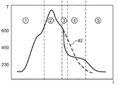
도 1은, 예를 들어, 저하 또는 재생과 같은 개별적인 상태 사이에 연관된 전이 및 실리콘 기판 내의 결함 상태가 설명될 수도 있는, 3 상태 모델(three-state model)을 나타낸 것이다.
도 2는, 본 발명의 실시형태에 따른 광기전력 소자의 생산의 상황 내의 실리콘 기판을 처리하기 위한 디바이스를 나타낸 것이다.
도 3은, 도 2에 나타낸 디바이스를 통해 통과 동안의 기판의 온도 프로파일을 나타낸 것이다.
상기 도면은, 단지 도식적으로 나타낸 것이고, 규모에 충실하지 않다. 도면에서, 이러한 참고 번호는 동일한 것 또는 동일한 효과를 가지는 특징을 나타낸다. The above-described and further possible aspects, features and advantages of the present invention will be apparent from the following description of specific embodiments with reference to the accompanying drawings, and it is to be understood that any description and drawings are not intended to limit the invention.
FIG. 1 illustrates a three-state model in which a transition between an individual state, such as, for example, degradation or regeneration, and a defect state in a silicon substrate may be described.
2 shows a device for processing a silicon substrate in the context of production of a photovoltaic device according to an embodiment of the present invention.
Figure 3 shows the temperature profile of the substrate during passage through the device shown in Figure 2;
The figures are only schematic and are not to scale. In the drawings, these reference numerals denote features which are the same or have the same effect.
본 발명의 선호되는 실시형태의 서술DESCRIPTION OF PREFERRED EMBODIMENTS OF THE PRESENT INVENTION
본원의 하기에 기재된 본 발명의 실시형태는, 가장 넓은 의미에서의 예를 들어, 태양 전지 및 태양광 모듈(solar modules)과 같은, 실리콘-기초된 광기전력 소자에서 무해한 전기학상으로 활동적인 결함을 제공하거나 부동태화(passivating)를 위한 방법에 관한 것이다. 특히, 상기 결함은, 상기 태양 전지(조명 하의 효율, 전류, 전압)의, 특히 단결정의, 뿐만 아니라 또한 일반적으로 다결정 실리콘 또는 태양 전지의, 이에 대해 의존적인 것인, 출발 물질 및 전기 성능 파라미터의 품질(소수 전하 캐리어의 (통계적인) 수명에 의해 기재됨)을 상당히 감소시킬 수도 있는, 문헌에 기재된 바와 같은, 붕소-산소 연관된 결함일 수도 있다. 본원에 제안된 상기 방법의 작용은, 그 밖의 결함에서 너무 배제되는 것은 아니다. Embodiments of the invention described herein below provide innate electrophysiologically active defects in silicon-based photovoltaic devices, such as, for example, solar cells and solar modules, in the broadest sense And a method for providing or passivating the same. In particular, the defects are related to the dependence of the starting materials and electrical performance parameters of the solar cell (efficiency, current, voltage), in particular of monocrystals, as well as of polycrystalline silicon or solar cells, May be a boron-oxygen associated defect as described in the literature, which may significantly reduce the quality (as described by the (statistical) lifetime of the minority charge carriers). The action of the method proposed herein is not so excluded from other defects.
태양 전지 또는 태양광 모듈은, 중간 형태로서 열 사용 없이 부수적인 자외선/가시광선/적외선의 에너지를 전기적으로 사용가능한 에너지로 전환하기 위해 사용된다. 상기 내부의 광 효과(photo effect)는, 반도체 물질(예를 들어, 실리콘)에서의 전자가, 활동적으로 방해된 밴드 갭을 넘어서 전자기 방사선에 의해 여기되고, 이에 따라 상기 반도체의 밴드 갭에 상응하는 에너지를 적어도 흡수하는 것을 목적으로 사용된다. 본 분야의 통상의 기술자는, 여기된 (현재 이동성이 있는) 전자가 이의 원래의 원자를 떠나고, 그리고 난 다음에 상기 원래(중성의) 원자는 과잉 양전하("분실한" 전자 = 홀)이 남아있기 때문에, 이런 연유로 전자-홀 쌍의 여기를 나타낸다(The person skilled in the art refers in this connection to the excitation of an electron-hole pair, because the excited (now mobile) electron leaves its original atom and the original (neutral) atom is then left with an excess positive charge (a "missing" electron = hole)). 여기된다면, 이동 전자(mobile electron)가 (양전하된) 원자에 의해 또 다시 포획되고(trapped), 중간에 있어서 저장된 에너지(상기 밴드 갭에 상응하는)는 또 다시 상실된다. 이러한 경우에 본 분야의 통상의 기술자는, 전자-홀 쌍의 재결합(recombination)을 나타낸다. 재결합 작동은 적어도 하나의 전자 및 하나의 홀을 필연적으로 필요로 한다. Solar cells or photovoltaic modules are used as intermediate forms to convert energy from incidental ultraviolet / visible / infrared rays into electrically usable energy without the use of heat. The internal photo effect is such that electrons in a semiconductor material (e.g., silicon) are excited by electromagnetic radiation beyond the band gap that is actively impeded, It is used to at least absorb energy. One of ordinary skill in the art will recognize that the excited (currently mobile) electron leaves its original atom and then the original (neutral) atom remains an excess positive ("lost" electron = hole) This is why the electron-hole pair is referred to as the electron-hole pair (because it is the electron-hole pair) (a "missing" electron = hole)). If excited, the mobile electron is trapped again by (positively charged) atoms, and the stored energy in the middle (corresponding to the bandgap) is again lost. In this case, a person skilled in the art will recognize the recombination of electron-hole pairs. The recombination operation inevitably requires at least one electron and one hole.
사용가능한 빛의 포획된 에너지를 제공하기 위해, 전자 및 홀은 서로 분리되어야 한다. 일반적인 태양 전지에서, 이는, 구성요소에서 서로 인접한 전자-풍부(n-타입 도핑된) 영역[electron-rich (n-type doped) region] 및 전자-고갈된 홀-풍부(p-타입 도핑된) 영역[electron-depleted hole-rich (p-type doped) region]을 배열하고, 소위 pn 접합을 형성함으로써 달성된다. 인접한 영역에서 이동 전자 또는 홀의 농도 차이 및 상기 전하 운반체의 결과적으로 형성된 확산으로 인하여, 전위 기울기는 상기 pn 접합에서 형성된다. 이러한 잠재적인 기울기는, 재결합이 억제의 결과로서, 전자-홀 쌍의 공간적인 분리를 가능하게 하고, 상기 저장된 에너지는, 양극성에 따라 분리된 이에 상응하여 배열된 금속 접촉을 통해 외부의 소비자에게 이용될 수도 있다. 보다 상세한 기재는, 상기 설정된 문헌에서 발견될 것이다. In order to provide the captured energy of the available light, electrons and holes must be separated from each other. In a typical solar cell, it is desirable to have an electron-rich (n-type doped) region and an electron-depleted hole-rich (p-type doped) Electron-depleted hole-rich (p-type doped) region], and forming a so-called pn junction. Due to the difference in concentration of moving electrons or holes in the adjacent region and the resulting diffusion of the charge carriers, the potential gradient is formed at the pn junction. This potential slope enables spatial separation of the electron-hole pairs as a result of the recombination inhibition, and the stored energy is used by external consumers through metal contacts arranged in a correspondingly separated manner according to the polarity . A more detailed description will be found in the established literature.
발생하기 위한 전자-홀 쌍의 이러한 공간 분리를 위해, 소수 전하 캐리어, 다시 말해서 반도체 기판의 흡수체 물질의 상기 반도체 타입과 상호 보완적인 전하 캐리어는, 상기 흡수체 물질에서 상기 pn 접합의 영역으로 확산할 수 있어야 한다. 만약 상기 흡수체 물질이, 전자 및 홀이 서로 교대로 결합될 수도 있고, 따라서 재결합 공정(recombination process)을 가져올 수도 있는 다수의 재결합-활동적인 결함을 가진다면, 그렇지 않으면 전기적으로 사용가능한 에너지는, 외부의 소비자에게 상실되고, 상기 태양 전지의 전기적인 성능은 악화된다. For this spatial separation of the electron-hole pair to occur, a charge carrier, i.e. a charge carrier, which is complementary to the semiconductor type of the absorber material of the semiconductor substrate, can diffuse from the absorber material to the region of the pn junction . If the absorber material has a plurality of recombination-active defects, in which the electrons and holes may be alternately combined with each other and thus may lead to a recombination process, And the electrical performance of the solar cell deteriorates.
결함의 밀도, 또는 전자-홀 쌍의 결과로 초래된 (쉽게 측정가능한) 수단 수명은, 따라서, 그것으로부터 생산된 상기 태양 전지의 전기적 성능 및 반도체 물질의 품질에 대한 중요한 파라미터이다. The density of the defect, or the resulting (easily measurable) means life resulting from the electron-hole pair, is therefore an important parameter for the electrical performance of the solar cell produced therefrom and the quality of the semiconductor material.
태양 전지에 대해, 결정질 실리콘은, 전자-홀 쌍이 발생되는 흡수체 물질로서 사용될 수도 있다. 본 분야의 통상의 기술자는 단결정 및 다결정 물질을 구별하고, 다결정 물질은 사용된 상기 생산 공정 때문에, 다수의 개별적인 결정으로 구성된 것이다. 상기 상이한 생산 공정은 이렇게 함으로써 상기 물질의 상이한 특징을 결정한다. For solar cells, crystalline silicon may also be used as an absorber material from which electron-hole pairs are generated. One of ordinary skill in the art distinguishes between monocrystalline and polycrystalline materials, and polycrystalline materials are made up of a number of individual crystals because of the production process used. The different production process thus determines the different characteristics of the material.
단결정 실리콘의 경우에, 초크랄스키(Cz-Si)에 따른 공정이 주로 사용되고, 단일 실리콘 결정은 상기 용해된 실리콘으로부터 당겨진다. 상기 사용된 미가공의 실리콘은 주로 매우 순수하고, 주목할 만한 오염물질, 특히 산소가 없는 것이다. 그러나, 초크랄스키 공정에서, 상기 실리콘의 높은 화학적 반응성, 상기 사용된 온도(실리콘의 용해 온도: 1410 ℃), 용해에서의 관습적인 방식(convention in the melt) 및 도가니의 회전에 의해 공격을 받고, 상기 잔류한 용해물 내로 부분적으로 용해된다. 이러한 것은 일반적으로, 석영 도가니로부터 산소가 바람직하기 않게 상기 용해물에서 축적되고, 이질적인 물질 오염물질로서 상기 단일 실리콘 결정 내로 포함되는 결과를 가진다. 일반적으로, Cz-Si의 격자 사이의 산소 함량(interstitial oxygen content)은, 5 x 10¹⁷ 내지 3 x 1018 cm-3의 범위에 있다. 상한 치수는, 용해도에 의해 제공된다. 초크랄스키 공정에서, 전체로서 상기 결정에서 더 낮은 산소 농도는, 예를 들어, 용해물에서 대류를 방해하는 자기장에 의하여, 추진된 방법에 의해서만 쉽게 달성될 수도 있다. In the case of monocrystalline silicon, a process according to Cz-Si is mainly used, and a single silicon crystal is drawn from the dissolved silicon. The raw silicon used is primarily very pure, with no noticeable contaminants, especially oxygen. However, in the Czochralski process, the high chemical reactivity of the silicon, the temperature used (melt temperature of silicon: 1410 ° C), the convention in the melt and the rotation of the crucible , And is partially dissolved into the remaining melt. This generally has the consequence that oxygen from the quartz crucible is undesirably accumulated in the melt and is incorporated into the single silicon crystal as a heterogeneous material contaminant. Generally, the interstitial oxygen content between Cz-Si lattices is in the range of 5 x 10 17 to 3 x 10 18 cm -3 . The upper limit dimension is provided by solubility. In the Czochralski process, the lower oxygen concentration in the crystals as a whole may be easily achieved only by the propelled method, for example by a magnetic field which interferes with convection in the melt.
매우 순수하고, 또한 특히 전자 산업을 위해 낮은-산소 단일 실리콘 결정을 제공하는 "플롯-존(float-zone)" 공정에 의해 생산된 단결정 물질은, 높은 비용으로 인하여 실리콘-기초된 태양 전지의 생산에서 좀처럼 사용되지 않는다. Monocrystalline materials produced by a "float-zone" process that is very pure and also provides low-oxygen single silicon crystals, especially for the electronics industry, are expensive because of the production of silicon- It is rarely used in.
다결정 실리콘은 상이한 공정에 의해 일반적으로 생산되고, 용해된 실리콘은, (코팅된) 석영 주형(예를 들어, 브릿지만 공정(Bridgeman process))에서 1 방향으로 결정체를 이루고, 다수의 미결정은 일반적으로 단일 결정을 대신하여 형성한다. 초콜라스키 공정과 대조적으로, 상기 용해물은 이러한 경우에 회전하지 않고, 대류 움직임이 더 작아진다. 이러한 이유에서, 상기 사용된 석영 주형은, 상기 용해된 실리콘에 의해 덜 공격을 받고, 보다 적은 산소가 상기 용해된 실리콘 내로 이동한다. 상기 공정에 따라, 상기 다결정 물질의 상기 산소 함량은 초콜라스키 공정에서보다 더 낮고, 전형적으로 5 x 10¹⁶ 내지 5 x 1017 cm-3의 범위에 있다. 그러나, 적절한 실행과 함께, 상기 미결정은 나중에 생산된 상기 태양 전지의 크기에 도달할 수도 있고, 그 결과 이는 사실상 단결정 물질이다. 본 분야의 통상의 기술자는, 유사-단결정 물질, 그러나 상기 초크랄스키 공정에 의해 생산된 물질과 비교된 보다 낮은 산소 함량을 가질 수도 있는 물질을 나타낸다. The polycrystalline silicon is generally produced by a different process and the dissolved silicon forms crystals in one direction in a (coated) quartz mold (for example, the Bridgeman process), and a plurality of microcrystals generally It is formed instead of a single crystal. In contrast to the chocolus process, the melt does not rotate in this case and the convection motion becomes smaller. For this reason, the quartz mold used is less attacked by the dissolved silicon and less oxygen is transferred into the dissolved silicon. According to this process, the oxygen content of the polycrystalline material is lower than in the chocolates process, typically in the range of 5 x 10 16 to 5 x 10 17 cm -3 . However, with proper implementation, the crystallization may reach the size of the solar cell produced later, resulting in a substantially single crystal material. Conventional art in the field refers to quasi-single crystal materials, but materials that may have lower oxygen content compared to materials produced by the Czochralski process.
인접한 미결정 사이의 결정 경계가 강한 재결합 중심으로서 작용하고, 관점의 공정 포인트로부터 문제가 있을 수도 있기 때문에, 상기 다결정 물질의 품질은 이에 대응하는 단결정 물질의 품질보다 낮다(The quality of the multicrystalline material is often lower than that of the corresponding monocrystalline material because the grain boundaries between adjacent crystallites act as strong recombination centres and may be problematic from a process point of view). 이러한 것은, 단결정 태양 전지가 일반적으로 비교가능한 다결정 태양 전지보다 높은 효율을 가지는 결과를 가진다. The quality of the polycrystalline material is lower than the corresponding quality of the single crystal material because the crystal boundary between adjacent crystallites acts as a strong recombination center and may be problematic from a point of view point of view and (b) the corresponding monocrystalline material due to the intercalated crystallites between adjacent grains. This results in that a single crystal solar cell has higher efficiency than a generally comparable polycrystalline solar cell.
pn 접합을 생산할 수도 있도록, 상기 흡수체 물질은 도핑되어야 한다. 상기 생산된 물질은, 인이 도판트로서 주로 사용되는 경우에, 전자-풍부(n-타입), 또는 붕소 또는 갈륨이 도판트로서 선택되는 경우에, 홀-풍부(p-타입)일 수도 있다. 그러나, 결정 및 용해물에서 이의 보다 나은(거의 동일한) 용해성 행동으로 인하여, 붕소는 상기 실리콘 결정의 성장 방향에 따라 갈륨보다 더 균일하게 분포되고, 따라서, 갈륨보다 도판트로서 보다 널리 사용된다. 의도적으로 또는 비의도적인 혼합된 도핑이 또한 통상적이다. 통상적인 도핑은 1 x 10¹⁴ 내지 1 x 1017 cm-3의 범위에 있고, 상기 수치는 상기 흡수체 물질의 양극성, 상기 태양 전지의 구성에 따라 구체적으로 사용된다. The absorber material must be doped so that it can also produce a pn junction. The produced material may be electron-rich (n-type) when phosphorus is mainly used as a dopant, or hole-rich (p-type) when boron or gallium is selected as a dopant . However, due to their better (nearly identical) solubility behavior in crystals and lysates, boron is more uniformly distributed than gallium according to the growth direction of the silicon crystals, and is therefore more widely used as a dopant than gallium. Intentional or unintentional mixed doping is also common. Typical doping is in the range of 1 × 10 14 to 1 × 10 17 cm -3 , and the numerical value is specifically used depending on the polarity of the absorber material, the configuration of the solar cell.
붕소 및 산소가 상기 실리콘 결정에 동시에 존재하는 경우에, 붕소-산소 연관된 결함은, 조명 또는 전하 캐리어 주입 하에, 다시 말해서 태양 전지 및 모듈의 전형적인 작업 조건 하에서, 실온에서 수 시간 내에 활성화되거나 형성될 수도 있는 것으로 추가적으로 알려져 있고; 강한 재결합-활성 중심으로서 이러한 결함은, 상기 소수 전하 캐리어의 수명, 따라서 또한 상기 태양 전지/태양광 모듈의 전기적 성능을 제한할 수도 있다. 이러한 연유로, 본 분야의 통상의 기술자는, 붕소-산소 연관된 결함[도 1을 참고하라: 저하에 의해 비활성(어닐 처리된) 상태 A에서 활성(저하된) 상태 B로의 전이(transition from the inactive (annealed) state A by degradation to the active (degraded) state B)] 또는 붕소-산소 관련된 결함에 의한 제한을 나타낸다. 붕소-산소 관련된 결함 뿐만 아니라 그 밖의 조명-유도된 결함으로 인한 것은, 덜 정확한 표현 빛-유도된 결함은, 또한 공통의 이러한 이유로 인한 것이다. In the case where boron and oxygen are simultaneously present in the silicon crystal, the boron-oxygen associated defect may be activated or formed within hours of room temperature, under illumination or charge carrier injection, i. E. Under typical operating conditions of solar cells and modules Additionally known as having; Such defects as strong recombination-active centers may limit the lifetime of the hydrophobic charge carriers, and thus also the electrical performance of the solar cell / photovoltaic module. For this reason, one of ordinary skill in the art will understand that boron-oxygen associated defects (see FIG. 1: transition from the inactive (annealed) state A to active (degraded) state B by degradation (annealed state) degradation to the active (degraded) state B)] or boron-oxygen related defects. Due to boron-oxygen related defects as well as other light-induced defects, less accurate representation of light-induced defects is also due to this common cause.
상기 활성화된 및 따라서 재결합-활성 붕소-산소 관련된 결함(도 1을 참고하라: 상태 B)은, 어둠에서 100 내지 200 ℃ 또는 100 내지 300 ℃의 짧은 시간 동안 열을 가함으로서 또 다시 재결합-비활성 상태로 전환(도 1을 참고하라: 어닐링에 의해 활성 상태 B에서 상기 비활성 상태 A로의 전환)될 수도 있다. 그러나, 상기 붕소-산소 관련된 저하는, 상기 결함이 준안정(metastable)으로 또한 불리도록, 회복된 조명 또는 전하 캐리어 주입으로 또 다시 진행한다. The activated and thus recombination-activated boron-oxygen related defects (see FIG. 1: state B) can also be achieved by heating in the dark for a short time between 100 and 200 ° C. or between 100 and 300 ° C., (See FIG. 1: transition from active state B to inactive state A by annealing). However, the boron-oxygen related degradation proceeds again with restored illumination or charge carrier injection such that the defect is also referred to as metastable.
상기 (활성화된) 결함의 비중은, 상기 실리콘 기판에서, 붕소 농도에 대략 선형적으로(linearly) 달라지고, 산소 농도에 따라 대략 이차식적으로(quadratically) 달라진다. 따라서, 이러한 효과는, 특히, 초크랄스키 공정에 의해 생산된 붕소-도핑된 산소-풍부 실리콘 물질에 관련된 것이다. 많이 도핑된(붕소 함량 1 x 10¹⁶ 또는 적어도 2 x 1015 cm-3), 산소-풍부(함량 1 x 10¹⁸ 또는 적어도 5 x 1017 cm-3) 기판을 기초로 한 태양 전지의 경우에, 상기 효율은 이로 인하여 현저하게 감소될 수도 있다(~ 1 %abs 효율 손실). 구체적인 저하 손실은 사용된 태양 전지의 구성에 따라 다양할 수도 있다. The specific gravity of the (activated) defects varies substantially linearly with the boron concentration in the silicon substrate and varies approximately quadratically with oxygen concentration. Thus, this effect is particularly relevant to the boron-doped oxygen-rich silicon material produced by the Czochralski process. In the case of solar cells based on heavily doped (boron content 1 x 10 16 or at least 2 x 10 15 cm -3 ), oxygen-rich (content 1 x 10 18 or at least 5 x 10 17 cm -3 ) substrates , The efficiency may be significantly reduced (~ 1% abs efficiency loss). The specific degradation loss may vary depending on the configuration of the solar cell used.
그러나, 전형적으로 더 낮은 산소 오염물질을 가지는 다결정 실리콘 물질은 또한, 붕소가 우세한 도판트가 아닌 실리콘 물질, 특히 붕소 첨가로 부분적으로 보충된 인-도핑된 물질이 하는 것처럼, 효과를 나타냄을 또한 보여주고 있다(It has also been shown, however, that multicrystalline silicon materials having typically lower oxygen contamination also exhibit the effect, as do silicon materials in which boron is not the dominant dopant, in particular also phosphorus-doped partially compensated materials with boron additions).However, polycrystalline silicon materials, which typically have lower oxygen contaminants, also show an effect as a boron doped silicon material, in particular boron doped, partially doped phosphorous doped material In the case of boron doping, it is also possible to reduce the amount of boron to be added to the boron. ).
지금까지, 붕소-산소 연관된 저하의 문제를 해결하거나 피하기 위한 4 가지 접근법이 특히 알려져 있다. So far, four approaches to solving or avoiding the problem of boron-oxygen related degradation are particularly known.
첫 번째 접근법은, 실리콘 결정의 원하지 않는 산소 오염을 최소화함으로써 출발한다. 한편으로는, 석영 도가니의 신규한 코팅은, 이의 용해를 예방하기 위한 것이다. 다른 한편으로는, 특히 초크랄스키 공정에서, 상기 석영 도가니로부터의 물질의 제거가 최소화될 수도 있는 것의 결과로서, 자기장은, 상기 용해된 실리콘의 대류 움직임이 상기 석영 도가니에서 직접적으로 억제되는데 사용된다. 이에 부응하여 생산된 MCz 실리콘은, 1 x 10¹⁷ 내지 5 x 1017 cm-3의 범위에서 이에 해당하는 보다 낮은 산소 농도를 가진다. 그러나, 상기 생산 공정은 일반적으로 보다 비싸고, 상기 보통의 공정과 비교된 바와 같이 단점에 보다 취약하다. The first approach starts by minimizing unwanted oxygen contamination of silicon crystals. On the one hand, the novel coating of the quartz crucible is intended to prevent its dissolution. On the other hand, in particular in the Czochralski process, as a result of the fact that the removal of material from the quartz crucible may be minimized, the magnetic field is used so that the convective movement of the molten silicon is directly inhibited in the quartz crucible . The MCz silicon produced in response thereto has a lower oxygen concentration corresponding to the range of 1 x 10 17 to 5 x 10 17 cm -3 . However, the production process is generally more expensive and more vulnerable to disadvantages as compared to the conventional process.
두 번째 접근법은, 출발 물질에서 붕소의 농도를 감소시키는 것을 기초로 한다. 붕소-산소 연관된 결함에 의한 제한이 없는 잠재적인 효율이 약 1 x 1016 cm-3의 도핑에서 최대화되면서, 만약 상기 붕소-산소 연관된 저하가 고려된다면 보다 낮은 도핑에서만 최대치에 도달함을 상기 이론적인 계산은 나타낸다. 그러나, 보다 낮게 도핑된 물질이 보다 낮은 저하 손실을 당할지라도, 상기 최대 효율 가능성이 완전하게 이용되지 않을 수도 있도록, 상기 최대한의 효율 가능성이 도핑 감소(doping fall)로서 감소한다. 상기 실리콘 기판의 최적의 도핑은 상기 태양 전지의 구체적인 구성에 따라 달라진다. 이러한 접근은 특히, 산소-풍부한 Cz 실리콘의 경우에, 1 x 10¹⁵ 내지 5 x 1015 cm-3의 범위에서 붕소 농도를 가지는 물질을 사용한, 대부분의 제조자에 의해 현재 적용된 것이다. A second approach is based on reducing the concentration of boron in the starting material. As the potential efficiency without limitations due to boron-oxygen associated defects is maximized at a doping of about 1 x 10 16 cm -3 , it is believed that the theoretical The calculation is shown. However, even if the lower doped material is subject to a lower degradation loss, the maximum efficiency possibility decreases as a doping fall so that the maximum efficiency possibility may not be fully utilized. Optimum doping of the silicon substrate depends on the specific configuration of the solar cell. This approach is currently being applied by most manufacturers, especially in the case of oxygen-rich Cz silicon, using materials with a boron concentration in the range of 1 x 10 15 to 5 x 10 15 cm -3 .
세 번째 접근법에서, 상기 도판트 붕소는, 예를 들어 갈륨으로 대체된다. 갈륨이 사용된 경우에, 어떠한 해당하는 결함이 발생하지 않거나 또는 상기 결함이 재결합-비활성임을 나타낼 가능성이 있다. 그러나, 붕소와 달리, 갈륨은, 상기 결정화 방향 상에 균일하게 도핑된 결정을 생산하기 위한 기술적인 도전의 결과로서, 결정 및 용해에서의 최적의 용해도 행동(optimum solubility behaviour)을 가지지 않는다. 결점에 대한 상기 공정의 보다 높은 민감성 및 보다 많은 물질의 낭비 및 이에 따른 보다 높은 비용이 결과이다. 따라서, 이러한 접근이 경제적으로 실현가능할지 여부는 의심스럽다. In a third approach, the dopant boron is replaced by, for example, gallium. In the case where gallium is used, there is a possibility that no corresponding defect occurs or that the defect is recombination-inactive. However, unlike boron, gallium has no optimum solubility behavior in crystal and dissolution as a result of the technical challenge to produce crystals uniformly doped in the crystallization direction. The higher sensitivity of the process to defects and the waste of more material and hence higher costs are the result. Therefore, it is doubtful whether this approach can be economically feasible.
네 번째 접근법은, 상기 붕소-산소 연관된 결함이 전하 캐리어 주입, 다시 말해서, 저하, 또는 어둠 속에서의 가열, 다시 말해서 어닐링에 의해 서로 전환될 수도 있는, 비활성(도 1을 참고하라: 상태 A) 및 활성 상태(도 1을 참고하라: 상태 B)에서 뿐만 아니라, 현재의 지식에 따라면, 재생에 활성 상태 B로부터 형성되는, 세 번째 재결합-비활성 "재생된" 상태(도 1을 참고하라: 상태 C)를 나타낼 수도 있음을 사실의 사용을 이용한다[The fourth approach makes use of the fact that the boron-oxygen correlated defect may be present not only in an inactive (see Figure 1: state A) and an active state (see Figure 1: state B), which may be converted into one another by charge carrier injection, that is to say degradation, or heating in the dark, that is to say annealing, but also in a third recombination-inactive "regenerated" state (see Figure 1: state C) which, according to current knowledge, forms from the active state B by regeneration].A fourth approach is to use an inactive (see FIG. 1: state A), in which the boron-oxygen associated defects may be switched to each other by charge carrier injection, i. E., Degradation or heating in the dark, Inactive "regenerated" state (see Figure 1), which is formed from active state B in regeneration, as well as in the active state (see Figure 1: State A) and an active state (see Fig. 1 (b)). The state-of-the- see Figure 1: state B), which may be converted into one another by carrier injection, that is to say, the degradation, or heating in the dark, (see Figure 1: state C) which, acco rding to current knowledge, forms from the active state B by regeneration].
이러한 상태는, (a) 이러한 것은 약하거나 또는 무시해도 될 정도의 재결합 활성도를 소유하고, (b) 조명 또는 온도 < 150 ℃에서의 전하 캐리어 주입 하에, 다시 말해서, 결함의 갱신된 활성화(renewed activation), 초기에 존재하는 비활성 상태와 대조적으로 안정적이고, 따라서 저하가 발생하지 않는 것을 특히 특징으로 한다.This state can be achieved by (a) possessing recombination activity that is weak or negligible, (b) under charge carrier injection at illumination or temperature < 150 ° C, in other words renewed activation of the defect ), Which is stable in contrast to the initially inactive state, and therefore does not cause degradation.
본 지식에 따라, 활성 결함, 다시 말해서 상태 B의 비활성 세 번째 상태 C 로의 전환은, 50 내지 230 ℃의 범위에서 예를 들어, 약간 증가된 온도에서 순방향으로 상기 태양 전지의 작동 또는 조명에 의한 전하 캐리어 주입, 결함의 전환을 가속화하는 보다 높은 온도 또는 보다 많은 과잉 전하 캐리어 밀도를 필요로 한다. 상기 존재하는 결함의 전환으로 인하여, 산소 및 붕소 함량과 관련하여 이러한 접근에서의 어떠한 제한이 없다. According to this knowledge, the active defects, that is to say the transition from the state B to the inactive third state C, are carried out in the range of 50 to 230 ° C, for example at a slightly increased temperature in the forward direction, Carrier injection, higher temperatures to accelerate the switchover of defects, or higher excess charge carrier densities. Due to the conversion of the existing defects, there is no limitation in this approach with respect to oxygen and boron content.
활성 결함(상태 B)에서 상기 기재된 세 번째 "재생된" 상태 C로의 전환하는 공정은, "재생"으로서 하기의 본원에 나타내어 있고, DE 10 2006 012 920.2에 상세하게 기재되어 있고 청구되어 있다. The process of switching from active defects (state B) to the third described "regenerated" state C described above is described hereinbelow as "regeneration" and is described and claimed in detail in
재생 공정의 경제는, 재생된, 유리한 상태 C 로의 충분한 다수의 결함을 제공하기 위해 필요로 하는 시간의 기간, 또는 재생의 속도에 따라 실질적으로 달라진다. 따라서, 시간의 필요로 하는 기간을 감소시키고, 재생의 속도를 증가시킬 수 있는 공정은 많은 경제적인 관심이다. The economics of the regeneration process are substantially different depending on the duration of time required to provide a sufficient number of defects in the regenerated, favorable state C, or the rate of regeneration. Thus, processes that can reduce the time required for time and increase the speed of regeneration are of great economic interest.
"재생"으로서 나타낸 상기 공정이, 보다 효율적으로 다시 말해서, 보다 짧은 시간 및 보다 낮은 비용으로 수행될 수도 있도록, 광기전력 소자를 생산하기 위한 방법을 제공하는 것을 그 중에서도 본 발명의 목적으로 나타낼 수도 있고, 따라서, 실리콘-기초 태양 전지의 효율 가능성이 보다 좋게 사용될 수도 있다. 상기 기재된 생산 공정은 또한 실리콘에서 그 밖의 결함에도 작용하는 것이 제외되지 않고, 또한 약간의 개조가 사용될 수도 있다. It may be pointed out for the purpose of the present invention to provide a method for producing a photovoltaic device such that the process represented as "Regeneration" may be performed more efficiently, that is, for a shorter time and at a lower cost , And thus the efficiency of a silicon-based solar cell may be better used. The production process described above does not exclude that it also acts on other defects in silicon, and some modifications may also be used.
본 발명의 하나의 실시형태에 따라, 하기의 단계를 포함하는, 광기전력 소자, 예를 들어 사용가능한 태양 전지 또는 모듈 또는 전구체를 생산하기 위한 방법이 제공되어 있다: According to one embodiment of the present invention, there is provided a method for producing a photovoltaic device, for example a usable solar cell or module or precursor, comprising the steps of:
예를 들어, 붕소 또는 임의적으로 상이한 도판트로 도핑된 산소-함유 실리콘 기판을 제공하는 단계, 및 상기 실리콘 기판의 표면에 pn 접합을 형성하기 위한 에미터 층을 형성하는 단계로서, 이로 인하여, Providing an oxygen-containing silicon substrate doped with, for example, boron or optionally a different dopant, and forming an emitter layer for forming a pn junction on the surface of the silicon substrate,
(a) 수소는 상기 실리콘 기판 내로 도입되고,(a) hydrogen is introduced into the silicon substrate,
(b) 만약 구체적인 공정에서 필요로 한다면, 상기 기판은, 만약 어떠한 신선한 수소가 이러한 시기(phase)에 상기 실리콘 기판 내로 도입되지 않는다면, 오직 짧은 시간 동안 > 450 ℃의 온도를 경험하고,(b) if necessary in a specific process, the substrate experiences a temperature of > 450 DEG C for only a short time, if no fresh hydrogen is introduced into the silicon substrate in this phase,
(c) 상기 기판은 시간의 특정한 기간 동안에 230 내지 450 ℃의 온도 범위에서 임의적으로 유지되고, 과잉 소수 전하 캐리어는 이러한 시기 동안에 상기 기판에서 임의적으로 발생되고, 그 다음에, 임의적으로, (c) the substrate is optionally maintained at a temperature in the range of from 230 to 450 DEG C for a certain period of time, the excess hydrophobic charge carriers are generated randomly in the substrate during this period,
(d) 상기 기판은 온도 범위 50 내지 230 ℃에서 유지되고, 과잉 소수 전하 캐리어는 이러한 시기 동안에 발생된다. (d) the substrate is maintained at a temperature in the range of 50 to 230 DEG C, and excess hydrophobic charge carriers are generated during this period.
공정 단계 (d)는 DE 10 2006 012 920 A1에 따른 방법에 부합한다. 본원에 나타낸 부분적인 단계 (a) 내지 (c)를 가지는 방법은, DE 10 2006 012 920 A1에 기재된 공정이 최적화될 수도 있는 이러한 방식으로 광기전력 소자를 변경하는 것을 그 중에서도 목표로 하고, 따라서 경제적으로 매력적인 방식으로 진행될 수도 있다. Process step (d) meets the method according to
본 발명에 따른 방법에 사용된 상기 실리콘 기판은, 초크랄스키 공정에 의해 생산된 웨이퍼일 수도 있고, 1 x 10¹⁵ 내지 1 x 1017 cm-3의 범위에서 붕소 도핑을 가진다. 이러한 웨이퍼는, 예를 들어, 1 x 10¹⁷ 내지 3 x 1018 cm-3의 이의 생산으로부터 기인하여, 특정한 산소 농도를 가진다. 그러나, 상기 가스 또는 액체 상으로부터 캐리어 상에 증착된 예를 들어, 다결정 실리콘 웨이퍼 또는 실리콘 층과 같은, 그 밖의 붕소-도핑된, 산소-함유 실리콘 기판을 사용하는 것이 또한 가능하다. The silicon substrate used in the method according to the present invention may be a wafer produced by a Czochralski process and has a boron doping in the range of 1 x 10 15 to 1 x 10 17 cm -3 . Such a wafer has a specific oxygen concentration, for example, due to its production of 1 x 10 17 to 3 x 10 18 cm -3 . However, it is also possible to use other boron-doped, oxygen-containing silicon substrates, such as, for example, polycrystalline silicon wafers or silicon layers deposited on carriers from the gas or liquid phase.
전자-홀 쌍의 분리를 필요로 하는 전위 기울기(pn 접합)을 야기하기 위해, 에미터는 상기 실리콘 기판의 표면 상에 본 발명에 따라 형성된다. 이러한 것은, 상기 기판의 상기 반도체 유형에 상반되는 반도체 유형을 일반적으로 가지는 영역이다. 만약 붕소가 상기 기판에서 우세한 도판트라면, 상기 기판은 p-도핑된 것이다. 상기 기판의 상기 반도체 유형은, 만약 인과 같은, n-도핑 물질의 이에 대응하는 양이 존재한다면, 붕소 도핑에도 불구하고 n-타입임을, 배제할 수 없다. 상기 에미터의 형성은, 예를 들어, 인(p-타입 기판의 경우에) 또는 붕소(n-타입 기판의 경우에)과 같은 도판트의 표면적인 확산(superficial diffusion)에 의해 일어날 수도 있다. 이러한 확산은, 800 ℃ 이상의 온도에서 일반적으로 수행된다. 그러나, 상이한 방법은, 이에 대응하는 에미터 층을 생산하기 위해 또한 사용될 수도 있다. 예를 들어, 이에 해당하는 양극성의 에미터 층은, 기체 또는 액체 상 또는 플라즈마로부터 상기 기판 표면 상에 증착될 수도 있다. 에미터 층을 생산하기 위한 추가적인 가능성은, 이에 대응하는 물질의 합금일 수도 있다. 게다가, 상기 실리콘 기판의 표면은, 완전하게 뒤덮이지 않아야 한다. 에미터 층과 상기 전면 및/또는 후면 상의 표면의 부분적인 영역만을 덮는 것으로 충분할 수도 있다. Emitters are formed according to the present invention on the surface of the silicon substrate to cause a potential gradient (pn junction) that requires separation of the electron-hole pairs. This is an area that generally has a semiconductor type that is contrary to the semiconductor type of the substrate. If boron is a predominant dopant in the substrate, the substrate is p-doped. The semiconductor type of the substrate can not exclude that it is n-type, despite boron doping, if a corresponding amount of n-doped material, such as phosphorus, is present. The formation of the emitter may occur, for example, by superficial diffusion of a dopant, such as phosphorous (in the case of a p-type substrate) or boron (in the case of an n-type substrate). This diffusion is generally carried out at a temperature of 800 ° C or higher. However, different methods may also be used to produce corresponding emitter layers. For example, a corresponding bipolar emitter layer may be deposited on the substrate surface from a gas or liquid phase or from a plasma. A further possibility for producing the emitter layer may be an alloy of the corresponding material. In addition, the surface of the silicon substrate should not be completely covered. It may be sufficient to cover only a partial area of the emitter layer and the surface on the front and / or back surface.
상기 에미터 및 상기 기판이 상기 동일한 반도체 유형의 것인 경우는, 상기 원하는 가능한 기울기를 초래하는 밴드 밴딩(band bending)을 인터페이스에서 확립되도록, 예를 들어, 만약 상기 기판 및 상기 에미터 층이 매우 상이한 밴드 구조(헤테로 구조)를 가진다면, 또한 달성될 수도 있다. 경계선상의 경우에서, 이에 대응하는 선택된 금속이 이러한 밴드 밴딩(MIS 구조)를 또한 유도할 수도 있기 때문에, 반도체는 사용되어야 할 필요는 없다. If the emitter and the substrate are of the same semiconductor type, for example, if the substrate and the emitter layer are very close to each other so that band bending resulting in the desired tilt is established at the interface May also be achieved if they have different band structures (heterostructures). In the case of on the borderline, the semiconductor need not be used because the corresponding selected metal may also induce such band banding (MIS structure).
실리콘 결정이 수소의 충분한 양을 전형적으로 포함하지 않기 때문에, 실리콘 기판으로 수소의 도입은, 본 발명에 따른 방법의 상황 내에서 필수적이다. Since silicon crystals typically do not contain a sufficient amount of hydrogen, the introduction of hydrogen into the silicon substrate is essential in the context of the process according to the invention.
수소는 매우 넓은 다양한 방법에 의해 도입될 수도 있다. 예를 들어, 상기 수소는, 상이한 기능(예를 들어, 상기 표면의 패시베이션(passivation), 빈사방지 코팅)을 가질 수도 있고, 상기 실리콘 결정을 관통할 수도 있는, 수소화된 질화 실리콘(a-SiNx:H), 수소화된 탄화 실리콘(a-SiCx:H), 수소화된 산화 실리콘(a-SiOx:H), 수소화된 실리콘 산화 질소(a-SiOxNy:H), 수소화된 산화 알루미늄(Al2O3), 수소화된 비결정질 실리콘(a-Si:H) 또는 비교가능한 층과 같은, 하나 또는 둘 다의 면에 적용된 코팅으로부터의 온도 단계의 상황 내에 방출될 수도 있다. 특히, 상기 층에 결합된 수소가 방출되는 온도와 관련하여, 정확한 파라미터는, 층에서 층으로 다양하고, 상이한 실시형태에서 기재되어 있다. 비교가능한 층에 대한 해당하는 유사한 실시형태는, 본 분야의 통상의 기술자에게 분명할 것이다. Hydrogen may be introduced by a wide variety of methods. For example, the hydrogen may be hydrogenated silicon nitride (a-SiNx: silicon nitride), which may have different functions (e.g., passivation of the surface, anti- H), a hydrogenated silicon carbide (a-SiCx: H), hydrogenated silicon oxide (a-SiOx: aluminum-H), a hydrogenated oxide (Al 2 O 3): H ), hydrogenated silicon nitrogen oxide (a-SiOxNy , Hydrogenated amorphous silicon (a-Si: H), or a comparable layer. In particular, with respect to the temperature at which the hydrogen bound to the layer is released, the exact parameters vary from layer to layer and are described in different embodiments. Corresponding similar embodiments for comparable layers will be apparent to those of ordinary skill in the art.
상기 금속 접촉의 생산이 수소화된 코팅으로부터 수소의 방출을 또한 유도할 수도 있는 높은-온도 단계를 필요로 할 수도 있는 이러한 지점에서 언급되어야 한다. It should be noted at this point that the production of the metal contact may require a high-temperature step which may also lead to the release of hydrogen from the hydrogenated coating.
하나의 실시형태에 따라서, 상기 실리콘 기판으로 침투될 수 있는, 600 ℃ 이상의 온도에서 높은-온도 단계 동안에 재구조화되고, 원자 및 분자 형태에서의 수소를 방출하는, 수소원 수소화된 질화실리콘(a-SiNx:H)으로서 사용된다. 방출된 수소의 양은According to one embodiment, hydrogen-hydrogenated silicon nitride (a-Si), which is re-structured and emits hydrogen in atomic and molecular forms during high-temperature steps at a temperature of 600 ° C or higher, SiNx: H). The amount of hydrogen released is
(a) 높은-온도 단계 전에 상기 층의 조성,(a) the composition of the layer before the high-temperature step,
(b) 최대 온도,(b) maximum temperature,
(c) 온도 프로파일, 특히 높은-온도 단계의 기간(c) the temperature profile, in particular the duration of the high-temperature phase
에 따라 달라질 수도 있다. ≪ / RTI >
일반적으로, 보다 많은 수소가 보다 높은 온도에서 보다 빠른 속도로 방출된다. 게다가, 만약 상기 수소가 상기 기판의 도처에 분포되고, 또한 특히 상기 기판 내로 깊이 침투한다면, 이는 편리하다. Generally, more hydrogen is released at higher temperatures at a higher rate. Furthermore, it is convenient if the hydrogen is distributed all over the substrate and more particularly penetrates deep into the substrate.
상기 높은-온도 단계 동안에 상기 온도 관리는,During the high-temperature step,
(Ⅰ) 600 ℃ 초과의 온도가 수소의 방출을 유도하는 것을 달성하고, (I) a temperature above 600 < 0 > C is achieved to induce the release of hydrogen,
(Ⅱ) 상기 온도 관리 및 기간은 수소의 충분한 양이 상기 기판 내로 확산되도록 하고, 및 (II) the temperature management and duration allow a sufficient amount of hydrogen to diffuse into the substrate, and
(Ⅲ) 상기 기판에서의 수소의 분포가 보장하는, (III) the distribution of hydrogen in the substrate is ensured,
것을 선택하도록 한 것이다. .
예를 들어, 이러한 것은, 온도 > 750 ℃가 몇 초 동안 존재하는, 태양 전지의 상기 금속 접촉을 합금하는 공정의 상황 내에서 달성될 수도 있다. For example, this may be achieved in the context of the process of alloying the metal contact of the solar cell where the temperature > 750 DEG C exists for a few seconds.
논증은, 예를 들어, 수소화된 탄화실리콘, 수소화된 산화실리콘 또는 수소화된 실리콘 산질화물(hydrogenated silicon oxynitrides)과 같은, 높은-온도 단계의 상황 내에 수소를 방출하는 유사한 층과 유사하다. 상기 온도 관리의 이에 대응하는 유사한 개조는, 본 분야의 통상의 기술자에게 명백할 것이다. The argument is analogous to a similar layer that releases hydrogen within the context of a high-temperature step, such as, for example, hydrogenated silicon carbide, hydrogenated silicon oxide, or hydrogenated silicon oxynitrides. Corresponding similar modifications of the temperature management will be apparent to those of ordinary skill in the art.
추가적인 실시형태에 따라, 온도 > 250 ℃에서 온도 단계의 상황 내에, 상기 기판 내로 침투할 수도 있는, 수소를 방출할 수 있는, 수소원 수소화된 산화 알루미늄(Al2O3)으로서 사용된다. 여기에, 상기에 기재된 질화 실리콘의 경우와 유사하게, 최대 온도, 온도 프로파일 및 기간은, 상기 기판에서 충분히 높고 잘 분포된 수소 농도를 달성하기 위해, 이에 따라 선택될 것이다. 상기 기판에서 수소의 분포를 뒷받침하기 위해, 과잉 소수 전하 캐리어는 상기 온도 단계 동안에 상기 기판에 발생될 수도 있다. 이러한 것은, 예를 들어, 조명 또는 예를 들어, 외부 전류에서의 통과에 의해, 영향을 받을 수도 있다. According to a further embodiment, it is used as hydrogen-hydrogenated aluminum oxide (Al 2 O 3 ), which is capable of releasing hydrogen, which may penetrate into the substrate, within the context of a temperature step at a temperature> 250 ° C. Here, similar to the case of the silicon nitride described above, the maximum temperature, temperature profile and duration will be selected accordingly to achieve a sufficiently high and well-distributed hydrogen concentration in the substrate. To support the distribution of hydrogen in the substrate, an excess of minority charge carriers may be generated in the substrate during the temperature step. This may be influenced, for example, by illumination or passage through an external current, for example.
추가적인 실시형태에 따라, 수소화된 비결정질 실리콘(a-Si:H)은 수소원으로서 사용되고, 수소는 온도 > 100 ℃의 온도의 상황 내에 방출된다. 여기에, 예를 들어, 질화 실리콘 층 및 산화 알루미늄의 상기에 기재된 경우와 유사하게, 상기 최대 온도 및 온도 프로파일 및 기간은, 상기 기판에서 충분하게 높고 널리 분포된 수소 농도를 달성하기 위해, 이에 따라 선택될 것이다. 상기 기판에서 수소의 분포를 뒷받침하기 위해, 과잉 소수 전하 캐리어는 상기 온도 단계 동안에 상기 기판에서 발생될 수도 있다. 이러한 것은, 예를 들어 조명 또는 예를 들어 외부 전류에서의 통과에 의해 영향을 받을 수도 있다. According to a further embodiment, hydrogenated amorphous silicon (a-Si: H) is used as the source of hydrogen and hydrogen is released in a situation of temperature> 100 ° C. Here, similar to the above-described case of the silicon nitride layer and the aluminum oxide, for example, the maximum temperature and temperature profile and duration may be adjusted to achieve a sufficiently high and widely distributed hydrogen concentration in the substrate, Will be selected. To support the distribution of hydrogen in the substrate, an excess of minority charge carriers may be generated in the substrate during the temperature step. This may be influenced, for example, by illumination or passage through an external current, for example.
추가적인 실시형태에 따라서, 예를 들어, 상기에 언급된 층의 다층 시스템이 또한 사용될 수도 있다. 예를 들어, 상기 층 시스템은, 상기 기판에 인접한 층이 수소원으로서 제공되고, 적어도 하나의 추가적인 층이 이에 위치되는 이러한 형태로 있을 수도 있다. According to a further embodiment, for example, a multilayer system of the above-mentioned layers may also be used. For example, the layer system may be in such a form that a layer adjacent to the substrate is provided as a source of hydrogen, and at least one additional layer is located thereon.
상기 추가적인 층의 적어도 하나는 수소 확산 장벽층으로서 작용할 수도 있고, 다시 말해서, 추가적인 층은 밑에 있는 수소-함유 층보다 수소에 덜 투과시킬 수 있고, 높은-온도 단계의 상황 내의 그러한 층을 따라 수소의 확산이 상대적으로 느리게만 진행한다. 이러한 경우에, 이러한 층은 수소 반사면(hydrogen reflector)으로서 작용하고, 상기 수소원으로부터 방출된 상기 수소는 상기 기판에서 보다 좋게 유지된다. 상기 소스 층으로부터 수소의 산출량, 다시 말해서, 기판 내로 확산된 수소의 양 대 방출되는 양의 비율이 이러한 경우에 더 좋고, 나중에 논의된 바와 같이, 보다 낮은 온도에서 외부-확산이 또한 최소화되기 때문에, 유리하다. At least one of the additional layers may act as a hydrogen diffusion barrier layer, that is, the additional layer may be less permeable to hydrogen than the underlying hydrogen-containing layer, Proliferation proceeds only relatively slowly. In this case, this layer acts as a hydrogen reflector, and the hydrogen released from the hydrogen source remains better in the substrate. The amount of hydrogen output from the source layer, i. E. The ratio of the amount of hydrogen diffused into the substrate to the amount of hydrogen released, is better in this case, and as discussed later, since out- diffusion is also minimized at lower temperatures, It is advantageous.
다른 층이 상기 소스층에서 상기 기판으로 수소의 확산에 영향을 미치지 않는, 상기 소스 층 및 상기 기판 사이의 또 다른 층을 배치하는 것이 원칙적으로 또한 가능할 수 있다. 수소에 대한 장벽 층은, 특정한 경우에 동일한 위치에서 유사하게 가능하다. It may in principle also be possible to arrange another layer between the source layer and the substrate, where another layer does not affect the diffusion of hydrogen from the source layer to the substrate. The barrier layer for hydrogen is likewise possible at the same position in certain cases.
상기 기판 내로의 수소의 도입은 상이한 방식으로 또한 수행될 수도 있다. 예를 들어, 상기 수소는 상기 실리콘 기판 내로 주입될 수도 있고, 다시 말해서, 양성자는 이에 대응하여 가속화되고, 또한 상기 기판으로 향하여 발사된다. 상기 선택된 공정 파라미터, 특히 양성자의 에너지 뿐만 아니라 이의 양에 따라, 상기 기판에서의 수소 분포가 목적이 분명하게 생산될 수도 있다. 실제의 이온 주입은, 한편으로, 양성자의 깨짐이 발생할 수도 있는 결정 손상(crystal damage)을 치유하고, 다른 한편으로, 수소의 추가적인 재분배에 영향을 미칠 수도 있는, 높은-온도 단계 > 500 ℃가 뒤따른다. The introduction of hydrogen into the substrate may also be performed in a different manner. For example, the hydrogen may be implanted into the silicon substrate, i. E., The protons are accelerated correspondingly and fired toward the substrate. Depending on the selected process parameters, in particular the energy of the proton as well as its amount, the distribution of hydrogen in the substrate may be clearly produced. The actual ion implantation, on the one hand, has a high-temperature step > 500 ° C, which may heal crystal damage that may cause cracking of the proton and, on the other hand, Follow.
상기 기판 내로의 수소의 도입은, 예를 들어, 수소-함유 플라즈마에서 또는 수소로 풍부한 대기로부터의 원자 수소(atomic hydrogen)의 확산에 의해 또한 추가적으로 일어날 수도 있다. The introduction of hydrogen into the substrate may also occur additionally, for example, by diffusion of atomic hydrogen from a hydrogen-rich plasma or from a hydrogen-rich atmosphere.
게다가, 상기 실리콘 기판으로 수소를 도입하는 그 밖의 방법은, 이들이 본원에 명쾌하게 언급되지 않을지라도, 또한 가능하다. In addition, other methods of introducing hydrogen into the silicon substrate are also possible, although they are not explicitly mentioned herein.
본 발명에 따른 방법의 상황 내에, 도입된 수소의 충분한 양이 상기 기판에 잔여하는 것이 추가적으로 바람직하다. 그 목적을 달성하기 위해, 그렇지 않다면, 수소 확산이 그렇지 않으면 중요한 정도로 발생하기 때문에, 상기 기판은, 상기-언급된 또는 그 밖의 소스로부터의 신선한 수소가 이용가능하지 않는 한, 연장된 기간 동안에, 온도 > 400 ℃, 특히 > 450 ℃에 있지 않아야 한다. It is further preferred that within the context of the method according to the invention, a sufficient amount of introduced hydrogen remains on the substrate. To achieve its goal, otherwise, since hydrogen diffusion otherwise occurs to a significant extent, the substrate is heated for a prolonged period of time, unless fresh hydrogen from the above-mentioned or other source is available, > 400 ° C, especially> 450 ° C.
특히, 수소의 도입이 보다 높은 온도에서 필요로 하는 경우에, 예를 들어, 수소가 질화 실리콘과 같은 수소화된 층으로부터 방출되는 경우에, 상기 층이 상기 기판의 외부로 유출되는 것보다 상기 기판 내로 보다 낮은 수소를 방출하는, 온도 범위에서의 시간의 기간이 최소화되어야 한다. In particular, when the introduction of hydrogen is required at higher temperatures, for example, when hydrogen is released from a hydrogenated layer such as silicon nitride, the layer is deposited into the substrate The duration of time in the temperature range, which releases lower hydrogen, must be minimized.
이러한 것은, 보다 이동성이 있는 전하 상태에서의 수소를 배치할 수도 있고, 따라서 이의 유출을 뒷받침하기 때문에, 400 ℃ 이상, 특히 450 ℃ 이상의 온도에서 과잉 소수 전하 캐리어를 발생하는 것이 추가적으로 유리할 수도 있다. This may additionally be advantageous to generate excess hydrophobic charge carriers at temperatures of 400 DEG C or higher, especially 450 DEG C or higher, as hydrogen may be arranged in the more mobile charge state and thus supports its efflux.
수소화된 질화 규소 층(a-SiNx:H)이 수소원으로서 사용된 실시형태에 따라, 예를 들어, 400 ℃ 내지 450 ℃ 사이의 온도 범위 및 600-650℃를 피하는 것 및 온도 650 ℃ 이상 내지 온도 450 ℃ 이하의 짧은 시간에 기판 온도를 보다 낮추는 것이 적절하고, 이에 의하여, 3 K/s 초과, 보다 30 K/s 초과의 특히 550 ℃ 이상에서의 냉각 속도가 적절하다. According to embodiments where the hydrogenated silicon nitride layer (a-SiNx: H) is used as the source of hydrogen, for example, a temperature range between 400 [deg.] C and 450 [deg.] C and avoiding 600-650 [ It is appropriate to lower the substrate temperature in a short time at a temperature of 450 DEG C or less, whereby a cooling rate of more than 3 K / s, more than 30 K / s, especially 550 DEG C or more is appropriate.
이 점에서, 상기에 이미 기재된 바와 같이, 수소에 대한 적어도 하나의 확산 장벽 층을 가지는 실시형태는, 상기 수소가 논의되고 있는 > 400 ℃ 또는 > 450 ℃의 온도 범위에서도 상기 기판으로부터 유출되는 것을 예방하기 때문에, 특히 유리할 수도 있다. 이러한 경우에, 0.3 K/s 초과의 보다 낮은 냉각 속도가 또한 허용될 수도 있다. In this regard, embodiments having at least one diffusion barrier layer for hydrogen, as already described above, prevent the hydrogen from leaking out of the substrate in the temperature range of > 400 DEG C or > 450 DEG C It may be particularly advantageous. In this case, a lower cooling rate of more than 0.3 K / s may also be acceptable.
본 발명에 따른 방법의 상황 내에, 이는, 적어도 10 초 및 많아야 30 분의 시간의 특정한 기간 동안에 온도 범위 230 내지 450 ℃에서 상기 기판을 유지하는 것이 유리할 수도 있다. 이러한 것은, 예를 들어, 온도 램프(temperature ramp)의 형태로, 또는 예를 들어, 안정기(plateau)의 형태로 달성될 수도 있다. Within the context of the method according to the invention, it may be advantageous to maintain the substrate at a temperature range of 230 to 450 占 폚 for a specific period of time of at least 10 seconds and at most 30 minutes. This may be achieved, for example, in the form of a temperature ramp or in the form of a plateau, for example.
상기 기판 온도로서 재생의 속도를 증가시키는 것의 본 발명에 따른 방법에 의해 달성되기 위한 원하는 효과가, 보다 짧은 처리 시간 내에 달성될 수도 있음이 발견되었다. 게다가, 재생의 속도를 증가시키는 원하는 효과를 위해, 상기 기판에서 과잉 소수 전하 캐리어를 발생하는 것이 원칙적으로 필요로 하지 않는다. 하기에 설명된 바와 같이, 또한 상기 전하 상태(charge state)를 조정함으로써 상기 언급된 온도 범위에서의 수소의 확산에 영향을 주기 위해, 상기 기판에서 과잉 소수 전하 캐리어를 발생하는 것이 그럼에도 불구하고 유리할 수도 있다. It has been found that the desired effect to be achieved by the method according to the invention of increasing the rate of regeneration as the substrate temperature may be achieved within a shorter treatment time. In addition, for the desired effect of increasing the speed of regeneration, it is in principle not necessary to generate excess hydrophobic charge carriers in the substrate. It may nevertheless be advantageous to generate an excess of minority charge carriers in the substrate, as described below, also to affect the diffusion of hydrogen in the above-mentioned temperature range by adjusting the charge state have.
하나의 실시형태에 따라, 상기 기판은, 과잉 소수 전하 캐리어의 발생 없이 230 내지 450 ℃의 범위의 온도에서 유지되고, 이에 의해 보다 높은 온도는, 상기 원하는 효과가 달성될 때까지, 상기 필요한 유지 시간을 감소시킨다. 그리고 난 다음에, 상기 기판은, 가파른 온도 램프(steep temperature ramp)를 가지는 실온으로 냉각된다. 상기 기판은 그 뒤에, DE 10 2006 012 920 A1에 기재된 바와 같이, 재생 공정으로 제공될 수도 있다. According to one embodiment, the substrate is maintained at a temperature in the range of 230-450 占 폚 without the occurrence of excess hydrophobic charge carriers, whereby the higher temperature is maintained until the desired effect is achieved, . Then, the substrate is cooled to room temperature with a steep temperature ramp. The substrate may then be provided in a regeneration process, as described in
또 다른 실시형태에 따라, 상기 기판은 과잉 소수 전하 캐리어의 발생 없이 230 내지 450 ℃의 범위에서의 온도에서 유지되고, 이에 의해, 보다 높은 온도는 상기 원하는 효과가 달성될 때까지, 필요한 유지 시간을 감소시킨다. 즉시 그 후에, 상기 기판은 50 내지 230 ℃의 온도 범위로 이동되고, 상기 재생 공정은, DE 10 2006 012 920 A1에 기재된 바와 유사한 방식으로 진행될 수도 있다. According to yet another embodiment, the substrate is maintained at a temperature in the range of 230 to 450 DEG C without the occurrence of an excess of small charge carrier, whereby a higher temperature is required to maintain the required holding time until the desired effect is achieved . Immediately thereafter, the substrate is moved to a temperature range of 50 to 230 DEG C, and the regeneration process may proceed in a manner similar to that described in
또 다른 실시형태에 따라, 상기 기판은, 예를 들어 조명에 의해, 과잉 소수 전하 캐리어의 발생과 함께 230 내지 450 ℃의 범위에서의 온도에서 유지되고, 이에 의해 보다 높은 온도는, 상기 원하는 효과가 달성될 때까지 상기 필요한 유지 시간을 감소시킨다. 재생의 속도를 증가시키는 것에 더하여, 특정한 상황 하에서 온도 > 230 ℃에서도 부분적인 또는 완전한 재생일 수도 있다. 즉시 그 후에, 상기 기판은 50 내지 230 ℃의 온도 범위로 이동되고, 상기 재생 공정은 필요에 따라 유지되고, 이미 부분적으로 발생되는 상기 재생으로 인하여 가속화된 방식으로 진행될 수도 있다. According to yet another embodiment, the substrate is maintained, for example by illumination, at a temperature in the range of 230 to 450 DEG C with the generation of an excess of small charge carrier, whereby a higher temperature is achieved, Thereby reducing the required holding time until it is achieved. In addition to increasing the speed of regeneration, it may also be a partial or complete regeneration, even at temperatures > 230 [deg.] C under certain circumstances. Immediately thereafter, the substrate is moved to a temperature range of 50 to 230 DEG C, and the regeneration process is maintained as needed, and may proceed in an accelerated manner due to the regeneration already occurring partially.
본 발명에 따른 방법의 완전한 실시형태는, 하기의 실시예를 거쳐 설명될 것이다. 이러한 실시형태에서, 수소화된 질화 실리콘은 수소원으로서 사용되고, 상기 층은, 실리콘 웨이퍼의 하나의 면에만 적용된 것을 가지고, 그 맞은편 면(opposite side)은, 알루미늄으로 완전하게 뒤덮힌 것이다. 반사방지 코팅 및 패시베이션 층으로 또한 작용하는, 상기 질화 실리콘 층 상에, 예를 들어, 높은 온도에서 상기 질화 실리콘 층을 공격하는, 스크린 프린팅(screen printing)에 의해 국부적으로 적용되고, 따라서, 밑에 있는 실리콘과의 접촉을 확립하는, 금속성 페이스트가 있다. 상기 질화 실리콘 층으로부터의 수소의 방출은, 벨트 용광로(belt furnace)에서 750 ℃ 이상에서 전형적으로 일어나는, 광기전력 소자의 금속화의 전형적인 합금 공정의 상황 내에 일어난다. A complete embodiment of the method according to the invention will be explained through the following examples. In this embodiment, the hydrogenated silicon nitride is used as the source of hydrogen, and the layer is applied to only one side of the silicon wafer, and the opposite side is completely covered with aluminum. Is applied locally by screen printing, which attacks the silicon nitride layer, for example, at a high temperature, on the silicon nitride layer, which also acts as an anti-reflective coating and a passivation layer, There is a metallic paste that establishes contact with silicon. The release of hydrogen from the silicon nitride layer occurs within the context of a typical alloying process of metallization of photovoltaic devices, which typically occurs above 750 占 폚 in a belt furnace.
도 2는, 태양 전지의 생산의 상황 내의 실리콘 기판의 처리를 위해 사용될 수도 있고, 본원에 기재된 상기 생산 방법의, 특히 이에 의해 수행될 안정화 처리 단계의 실시형태를 실행하기 위해 설계된, 특히 설정된 연속로 10의 형태에서의 디바이스를 나타낸 것이다. Fig. 2 is a diagrammatic view of a process for producing a solar cell, which may be used for the treatment of a silicon substrate in the context of the production of solar cells and which is designed to carry out the embodiments of the production process described herein, 10 shows a device in the form of FIG.
상기 연속로(10)는, 유도된 롤러(driven rollers)(12)에 의해 움직일 수도 있는 벨트(14)를 가진다. 주입구 면(16) 상에, 실리콘 기판이 상기 벨트(14) 위에 배치될 수도 있고, 그 다음에, 상기 연속로(10)의 상이하게 가열된 영역을 통해 상기 벨트(14)에 의해 움직여진다. 상기 실리콘 기판은, 이전에 수소-함유 층으로 이들의 표면 상에 제공될 수도 있다. 게다가, 금속-함유 페이스트의 패턴은 상기 수소-함유 층으로 프린트될 수도 있고, 이로 인하여 상기 태양 전지에 대한 상기 금속 접촉은 궁극적으로 형성될 것이다. The
예열하는 영역(18)에서, 상기 벨트(14) 상에 수송된 상기 실리콘 기판이 500 ℃ 이상까지의 온도로 예열될 수도 있는, 배열된 하나 또는 그 이상의 복사 난방기(radiant heaters)(20)가 있다. In the preheating
인접한 최대한의 가열 영역(22)에서, 이를 통해 통과하는 실리콘 기판이 700 ℃ 이상까지의 온도로 짧은 시간 동안 가열될 수도 있는, 적어도 하나의 추가적인 복사 난방기(22)가 제공된다. In the adjacent
그 후에 냉각 영역(26)이 있다. 냉각 영역(26)에서, 바람직하게는 어떠한 복사 난방기가 없을 뿐만 아니라, 이를 통해 통과하는 실리콘 기판이 능동적으로 냉각될 수도 있는 냉각 디바이스(28)가 제공된다. 상기 냉각 디바이스는, 예를 들어, 상기 냉각 영역(26)으로 차가운 질소 가스를 불기 위한 팬의 형태로 있을 수도 있다. Thereafter, there is a
온도 유지 영역(30)이 그 다음에 따른다. 온도 유지 영역(30)에서, 상기 실리콘 기판의 온도가 온도 유지 영역(30) 내의 230 ℃ 내지 450 ℃의 범위에 유지될 수도 있는, 추가적인 복사 가열기(32)가 제공된다. 상기 온도 유지 영역(30)의 길이가, 제공된 처리량 속도에서, 벨트(14)에 의해 수송된 실리콘 기판은, 상기 온도 유지 영역(30)을 통해 이동되도록, 적어도 10 초를 필요로 하는 것과 같을 수도 있고, 이에 의해 이는 230 내지 450 ℃의 온도 범위 내의 원하는 온도로 복사 난방기(32)에 의해 유지된다. 특히, 상기 온도 유지 영역(30)은, 예를 들어, 적어도 상기 최대 가열 영역(22)만큼, 바람직하게는 상기 최대 가열 영역보다 적어도 3 배, 바람직하게는 적어도 6 배 더 길 수도 있다. 전체로서 상기 연속로는, 예를 들어, 온도 유지 영역(30) 없이 통상적인 연속로의 2 배 이상일 수도 있다. The
상기 실리콘 기판은, 그 다음에 이를 추가적으로 냉각시킬 수도 있는 쿨링 다운 영역(cooling down zone)(34)에 도달한다. 상기 쿨링 다운 영역(34)에서, 적어도 0.3 kW/m2의 조명 강도로 이를 통과하는 상기 실리콘 기판을 비추기 위해서, 예를 들어, 보다 넓어진 레이저 빔을 가지는 레이저의 형태로, 또는 상기 실리콘 기판에 의해 흡수될 수도 있는 파장을 가지는 강한 램프의 형태로, 강한 광원(36)이 제공될 수도 있다. 상기 실리콘 기판이 적어도 상기 쿨링 다운 영역(34)의 출발에서 현저하게 90 ℃ 초과에 여전히 있기 때문에, 상기 재생 공정은 이로 인하여 영향을 받을 수도 있고, 궁극적으로 생산된 상기 태양 전지는 이들의 효율의 면에서 안정화될 수도 있다. The silicon substrate then reaches a cooling down
대안적으로 또는 게다가, 광원은, 상기 온도 유지 영역(30)에서 또한 제공될 수도 있다(도 2에 나타낸 실시형태에 제공되지 않음). 상기 온도 유지 영역(30)에서 이미 상기 실리콘 기판을 적절하게 조명함으로써, 상기 실리콘 기판 내로 침투되는 상기 수소가 임의적으로, 그 다음의 재생을 위해 유리한 상태를 추정하는데 임의적으로 뒷받침될 수도 있다. 다른 한편으로는, 상기 온도 유지 영역(30) 내의 이미 적절한 조명의 도움으로, 상기 실리콘 기판 내의 재생은, 적어도 부분적으로, 또는 임의적으로 또한 완전하게 적절한 공정 관리와 함께 수행될 수도 있다. Alternatively or additionally, a light source may also be provided in the temperature holding area 30 (not provided in the embodiment shown in Fig. 2). By appropriately illuminating the silicon substrate already in the
상기 연속로(10)의 원하는 구성 요소의 모두는, 공통의 제어 시스템(40)에 의해 바람직하게 조절될 수도 있다. All of the desired components of the
상기 실리콘 기판이 전체적인 연속로(10)을 통해 통과하는 경우에, 이들은, 배출구 면(38)에서 제거될 수도 있고, 추가적인 공정 또는 특성화 단계를 받을 수도 있다. If the silicon substrate passes through the entire
도 3은, 한 예로서, 상기 벨트 용광로(10)의 다양한 영역을 통해 상기 웨이퍼의 통과 동안에 온도 유지를 나타낸 것이다. Figure 3 shows, by way of example, the temperature maintenance during passage of the wafer through various regions of the
상기 벨트 용광로 내로의 들어감 및 상기 예열 영역(18)을 통한 통과에서(영역 1), 상기 실리콘 기판으로서 역할을 하는 상기 웨이퍼는 약 650 ℃에서, 이에 이전에 증착된 상기 수소화된 질화 실리콘 층으로부터 수소의 방출 및 상기 웨이퍼 내로 확산(영역 2)가 시작될 때까지, 첫 번째로 가열된다. 상기 최대 온도가 상기 최대 가열 영역(22)에 도달할 경우에, 상기 질화 실리콘 층으로부터의 수소의 방출이 또 다시 감소된다. 동시에, 상기 웨이퍼 내로 확산된 수소의 일부가 이미 또 다시 유출된다. 만약 온도가 대략 650 ℃ 이하로 떨어진다면, 상기 웨이퍼로부터의 유출은, 상기 질화 실리콘 층으로부터의 수소의 방출, 또는 상기 웨이퍼로의 확산을 초과하고, 상기 웨이퍼의 상기 수소 함량은 또 다시 떨어진다. 가능한 한 이러한 것을 예방하기 위해, 상기 웨이퍼는, 예를 들어, 20 K/s 초과의 높은 냉각 속도에서 가파른 온도 램프를 가지는 냉각 영역(26)(영역 3)에서 냉각되고, 상기 수소의 추가적인 유출이 억제된다. 상기 인접한 온도 유지 영역(30)에서 즉시 그 후에(영역 4), 상기 웨이퍼는 230 내지 450 ℃의 온도 범위에서 유지되고, 상기 기재된 방법에 따라, 나중의 재생 공정 단계에서 이 자체로 나타내는, 재생의 속도를 증가시키는 공정이 시작된다. 나중에 필요로 하는 상기 재생 시간은, 예를 들어, 영역 4에서 조명에 의해, 과잉 전하 캐리어를 발생시킴으로써 추가적으로 짧아질 수도 있다. 이러한 것은 절대적으로 필수적이지 않고, 본원에 기재된 방법 및 임의적으로 이미 포함되거나 분리하여 수행되는 DE 10 2006 012 920 A1에 따른 방법으로 이루어진 전체적인 공정의 경제에 이롭다. DE 10 2006 012 920 A1와 유사한 상기 재생 방법은 영역 5에 바로 뒤따를 수도 있다. 그러나, 이는 또한, 원한다면 분리하여 일어날 수도 있다. The wafer, acting as the silicon substrate in the entry into the belt furnace and in the passage through the preheating zone 18 (zone 1), is heated at a temperature of about 650 占 폚 to a hydrogen And the diffusion into the wafer (region 2) begins. When the maximum temperature reaches the
도 3에서, 예를 들어, 스크린 프린트된 접촉(screen printed contacts)의 착화(firing)를 위해 통상적으로 사용된 바와 같은, 통상적인 연속로를 통한 전형적인 온도 프로파일 파선(42)로서 첨가하여 나타낸 것이 있다. 상기 실리콘 기판은, 지속적으로 및 최대의 온도에 도달한 후에 대략 연속적으로 냉각됨을 나타낼 것이다. 450 ℃ 이상의 온도 범위 내의 체류 시간(dwell time)은 본 발명에 따른 연속로에서 보다 현저하게 더 긴 반면에, 230 ℃ 내지 450 ℃ 사이의 온도 범위 내의 체류 시간은 본 발명에 따른 연속로에서 보다 현저하게 더 짧다. In Figure 3, it is shown as a typical temperature profile dashed
본 발명의 실시형태의 추가적인 세부 사항, 특징 및 장점은, 근본적인 모델(underlying model)의 그 다음의 설명으로부터 본 분야의 통상의 기술자에게 명백할 것이다. Additional details, features and advantages of embodiments of the present invention will be apparent to those of ordinary skill in the art from the following description of the underlying model.
그 다음에, 모델은, 재생 공정의 시간 상수의 짧아짐(shortening)과 설명될 수 있음을 나타낼 것이다. 본 발명에 따른 방법에서 관찰된 재생의 속도에서의 증가 및 따라서 상기 재생 공정의 보다 효율적인 실행을 유도하는 정확한 인과관계의 관계는, 본 특허 출원을 준비하는 시간에 상세하게 이해되지 않음이 지적되고 있다. 따라서, 나타낸 모델은, 어떠한 방식으로, 첨부하는 청구항에 의해 정의된 바와 같이, 보호의 범위를 제한하려는 것은 아니다. The model will then show that it can be explained by a shortening of the time constant of the regeneration process. It is pointed out that the increase in the rate of regeneration observed in the method according to the invention and therefore the precise causal relationship leading to a more efficient performance of the regeneration process is not understood in detail at the time of preparing this patent application . Thus, the model shown is not intended to limit the scope of protection in any way, as defined by the appended claims.
본 발명자는, 상기 실리콘 결정에서 수소, 특히 이의 양, 이의 결합 상태 및 이의 전하 상태가, 예를 들어, 결함에 대한 수소의 부착에 의해, 상기 재결합-활성 결함에서 세 번째, 재생된 상태(상태 C)로의 전환에서의 결정적인 영향을 가짐을 추정한다. 결정 성장 후에 바로 상기 실리콘 결정에서 일반적으로 어떠한 수소가 없거나 너무 작은 수소가 있기 때문에, 수소는, 상기 재생 상태로의 전환을 가능하게 하기 위해, 상기 결정 내로 첫 번째로 도입되어야 한다. The present inventors have found that in the silicon crystal, hydrogen, particularly its amount, its bonding state and its charge state are changed from the recombination-active defect to the third, regenerated state (state C). ≪ / RTI > Since there is generally no or too little hydrogen in the silicon crystal immediately after crystal growth, hydrogen must first be introduced into the crystal in order to enable conversion to the regenerated state.
궁극적으로, 본 발명자는, 대략 450 ℃ 이하의 온도 범위에서 상기 실리콘 기판의 결정에서 현저하게 높은 농도로 있고, 측면으로 및 깊이의 면에서 둘 다 충분하게 균등으로 분포되어 있는 한, 상기 수소의 기원은 이러한 모델의 상황 내의 더 적은 중요성에 있는 것임을 추정한다. 대략 400 ℃ 이상 또는 대략 450 ℃, 수소는, 상기 실리콘 결정에서 주위로 현저한 정도로 여전히 벗어날 수도 있다. 본 발명에 다른 상기 기재된 생산 공정은, > 400 또는 > 450 ℃의 온도 범위로 생산 공정에서 상기 태양 전지를 잠시 노출시키는 것만을 고려하고, 상기 수소는 분산되지만, 신선한 수소는 예를 들어 층으로부터 공급되지 않는다. Ultimately, the present inventors have found that, as long as they are at a significantly higher concentration in the crystal of the silicon substrate in the temperature range of approximately 450 ° C or less and are sufficiently uniformly distributed both in terms of side and depth, Estimates that it is of less importance within the context of these models. At or above about 400 ° C, or about 450 ° C, hydrogen may still escape to a significant extent around the silicon crystal. The above described production process according to the present invention takes into account only a brief exposure of the solar cell in the production process to a temperature range of > 400 or > 450 DEG C, where the hydrogen is dispersed, It does not.
게다가, 본 발명자에 의한 연구는, 상기 수소의 결합 상태 또는 전하 상태가 결정적인 중요한 것이라는 것이 분명하다(studies by the inventors make it appear plausible that the bond state or charge state of the hydrogen is of critical importance). 이에 따라서, 상기 수소는, 적어도 두 가지의 상이한 결합 상태, 예를 들어, B-H 쌍으로서 붕소 원자에 결합된 또는 H2 분자의 형태의 형태로, 대부분 대략 500 ℃ 이하의 온도 범위에 존재할 수 있다. 그러나, 이러한 결합 형태에서 수소는 충분히 이동되지 않을 것이다. 상기 재생은, 수소의 분리, 원자 형태에서의 차후의 확산 및 붕소-산소 연관된 결함에 대한 부착에 대한 이러한 서술에 해당할 것이다. 재생의 속도, 다시 말해서, 상기 분해된 상태(상태 B)에서 결함에서 상기 재생된 상태(상태 C)로의 전환의 속도, 및 또한 진행하기 위한 상기 재생 공정에 대해 필요로 하는 시간의 기간은, 어떻게 상기 수소가, 전적으로 열의 지원 또는 또한 상기 전하 상태의 변화에 의해, 이의 결합된 상태로부터 쉽게 자유로울 수 있는지를, 그 중에서도 이러한 모델에 따라 달라진다. 본 발명에 따른 상기 기재된 생산 공정은, 수소의 충분한 양이 약간 결합된(전하 캐리어 주입 하의 적어도) 상태로만 존재하고, 따라서 상기 재생 공정에 대해 이용할 수 있음을 임의적으로 보장할 수도 있다. 게다가, 분열 후의 원자의 수소의 이동성은 이의 전하 상태에 따라 달라진다. p-타입 실리콘에서, 상기 수소는 일반적으로 양전하에 의해 전하되고, 이의 확산은 상기 결정 격자에서 정전 상호작용(electrostatic interaction)에 의해 저해된다. 다른 한편으로, 만약 수소가 중성의 전하 상태로 있다면, 이의 이동성은 현저하게 높아진다. 상기 전하 상태가 전하 캐리어 주입(전류에서의 통과시킴으로써 또는 조명)에 의해 조종될 수도 있다. 이에 따라서, 전하 캐리어 주입의 도움으로, 상기 수소의 이동성은, 이의 보다 높은 이동성 때문에, 보다 빠르게 상기 실리콘 결정에서의 결함에 도달하는데 영향을 미칠 수도 있고, 또한 이의 전하 상태 때문에 이들은 보호될 수도 있다(may also passivate them on account of its charge state). In addition, research by the present inventors has shown that the hydrogen bonding state or charge state is of crucial importance (studies by the inventors make it appear plausible that the bond state or charge state of the hydrogen is of critical importance). Accordingly, the hydrogen may be present in at least two different bonding states, for example in the form of a H 2 molecule bonded to a boron atom as a BH pair, mostly in a temperature range of about 500 ° C. or less. However, in this type of combination, hydrogen will not migrate sufficiently. Such regeneration will correspond to this description of the separation of hydrogen, subsequent diffusion in atomic form and attachment to boron-oxygen associated defects. The rate of regeneration, in other words, the rate of transition from defect to the regenerated state (state C) in the decomposed state (state B), and also the period of time required for the regeneration process to proceed, Whether the hydrogen can be freed from its combined state entirely by the support of heat or also by changes in the charge state depends in particular on such a model. The production process described above in accordance with the present invention may optionally ensure that a sufficient amount of hydrogen is present only in a slightly coupled state (at least under the charge carrier injection) and thus available for the regeneration process. In addition, the hydrogen mobility of the atom after cleavage depends on its charge state. In p-type silicon, the hydrogen is generally charged by positive charge, and its diffusion is inhibited by electrostatic interaction in the crystal lattice. On the other hand, if hydrogen is in a neutral charge state, its mobility is significantly increased. The charge state may be steered by charge carrier injection (by passing through current or by illumination). Accordingly, with the aid of charge carrier injection, the hydrogen mobility may affect the arrival of defects in the silicon crystal more quickly due to its higher mobility, and also because of their charge state they may be protected may also passivate them on account of its charge state).
어떠한 방식으로 본 발명을 제한하려는 의도는 아닌 것인, 단지 공식화(formulation)에서 추가적인 시도로서, 본 발명의 형태 및 실시형태의 기본적인 개념은 또한 하기에 기재될 수도 있다:The basic concepts of the forms and embodiments of the invention, which are merely an attempt at formulations, which are not intended to limit the invention in any way, may also be described below:
1. 하기의 단계를 포함하는, 결정질 실리콘에서의 전기적으로 활동적인 결함을 보호하는 증가된 능력 또는 속도를 가지는 광기전력 소자를 생산하기 위한 방법: 1. A method for producing a photovoltaic device having increased ability or speed to protect electrically active defects in crystalline silicon, comprising the steps of:
결함을 가지는 실리콘 기판을 제공하는 단계;Providing a silicon substrate having a defect;
상기 실리콘 기판의 표면 상에 에미터 층을 형성하는 단계;Forming an emitter layer on the surface of the silicon substrate;
수소는 상기 실리콘 기판으로 도입되고, 상기 실리콘 기판은 230 내지 450 ℃의 온도 범위에서 유지되는 것을 특징으로 한다. Hydrogen is introduced into the silicon substrate, and the silicon substrate is maintained in a temperature range of 230 to 450 ° C.
2. 유형 1에 따른 방법에서, 상기 실리콘 기판은 적어도 2초, 바람직하게는 적어도 10 초, 보다 바람직하게 적어도 30 초, 더욱 더 바람직하게는 적어도 90 초의 기간 동안 230 내지 450 ℃의 온도 범위에서 유지된다. 2. In the method according to
3. 상기에 기재된 어떠한 유형 중의 하나에 따른 방법에서, 상기 수소는 450 ℃ 이상의 온도에서 도입되고, 냉각하는 것(cooling)은, 450 ℃ 이상에서 적어도 3 K/s, 바람직하게는 10 K/s, 보다 바람직하게는 30 K/s, 더욱 더 바람직하게는 60 K/s의 램프로 일어난다. 3. The process according to any one of the preceding claims, wherein the hydrogen is introduced at a temperature of at least 450 DEG C and the cooling is at least 3 K / s, preferably 10 K / s , More preferably 30 K / s, even more preferably 60 K / s.
4. 유형 3에 따른 방법에서, 상기 냉각하는 램프는, 700 ℃ 내지 450 ℃의 온도 범위와 관련된 것이다. 4. Method according to
5. 상기에 기재된 어떠한 유형 중의 하나에 따른 방법에서, 과잉 소수 전하 캐리어는 상기 실리콘 기판에 발생된다. 5. In a method according to any of the above-described types, an excess of small charge carrier is generated in the silicon substrate.
6. 유형 5에 따른 방법에서, 상기 조명 강도는, 0.3 kW/m2 초과, 바람직하게는 1 kW/m2 초과, 보다 바람직하게는 3 kW/m2 초과이고, 파장 < 1180 nm를 가지는 빛이 사용된다. 6. The method according to
7. 상기에 기재된 어떠한 유형 중의 하나에 따른 방법에서, 상기 과잉 전하 캐리어는, 230 ℃ 내지 450 ℃, 또는 바람직하게는 230 ℃ 내지 400 ℃, 또는 보다 바람직하게는 230 ℃ 내지 350 ℃ 또는 더욱 더 보다 바람직하게는 230 ℃ 내지 300 ℃ 사이의 기판 온도에서 발생된다. 7. A method according to any one of the above-described aspects, wherein the excess charge carrier is heated to a temperature in the range of from 230 캜 to 450 캜, or preferably from 230 캜 to 400 캜, or more preferably from 230 캜 to 350 캜, Preferably between 230 [deg.] C and 300 [deg.] C.
8. 상기에 기재된 어떠한 유형 중의 하나에 따른 방법에서, 적어도 하나의 수소-함유 코팅은 수소원으로서 역할을 한다. 8. In the process according to any one of the types described above, the at least one hydrogen-containing coating serves as a source of hydrogen.
9. 유형 8에 따른 방법에서, 상기 수소-함유 코팅의 적어도 하나는 수소화된 질화 실리콘(hydrogenated silicon nitride)이다. 9. The method according to Type 8, wherein at least one of the hydrogen-containing coatings is hydrogenated silicon nitride.
10. 상기에 기재된 어떠한 유형 중의 하나에 따른 방법에서, 상기 수소는, 온도 650 ℃ 이상, 바람직하게는 700 ℃, 보다 바람직하게는 750 ℃에서 높은-온도 단계에 의하여 도입된다. 10. In a process according to any one of the above-described types, the hydrogen is introduced by a high-temperature step at a temperature of 650 ° C or higher, preferably 700 ° C, more preferably 750 ° C.
11. 상기에 기재된 어떠한 유형 중의 하나에 따른 방법에서, 상기 수소-방출 층은, 수소-방출 층보다 수소에 대한 낮은 투과성의 적어도 하나의 확산 장벽 층으로 덮여있다. 11. A method according to any one of the preceding claims, wherein the hydrogen-releasing layer is covered with at least one diffusion barrier layer which is less permeable to hydrogen than the hydrogen-releasing layer.
최종적으로, 용어 "포함하는", "가지는" 등은 추가적인 다른 요소의 존재를 제외하는 것이 아님을 언급되고 있다. 상기 용어 "하나" 또는 "a"는 또한, 다수의 요소 또는 대상의 존재를 제외하는 것이 아니다. 게다가, 상기 청구항에서 언급된 상기 방법 단계에 더하여, 추가적인 방법 단계는, 예를 들어, 태양 전지를 완성하기 위해 최종적으로 필수적이거나 유리할 수도 있다. 청구항에서 참고 숫자는, 단지 보다 나은 읽기 쉬움을 위한 것을 제공하는 것이고, 어떠한 방식으로 청구항의 보호의 범위를 제한하려는 것이 아니다. Finally, it is mentioned that the terms "including "," having ", and the like do not exclude the presence of additional elements. The terms " a "or" a "also do not exclude the presence of a plurality of elements or objects. In addition, in addition to the method steps mentioned in the claims, the additional method steps may ultimately be necessary or advantageous to complete the solar cell, for example. The reference numbers in the claims merely provide for better readability and are not intended to limit the scope of protection of the claims in any way.
참조 번호의 목록
A 어닐 처리된, 비활성 상태(annealed, inactive state)
B 저하된, 활성 상태(degraded, active state)
C 재생된, 비활성 상태(regenerated, inactive state)
(1)-(5) 가열 영역(heating zones)
10 연속로(continuous furnace)
12 유도된 롤러(driven rollers)
14 벨트(belt)
16 주입구 면(inlet side)
18 예열하는 영역(preheating zone)
20 복사 난방기(radiant heater)
22 최대 가열 영역(maximum heating zone)
24 복사 난방기(radiant heater)
26 냉각 영역(cooling zone)
28 냉각 디바이스(cooling device)
30 온도 유지 영역(temperature maintenance zone)
32 복사 난방기(radiant heater)
34 쿨링 다운 영역(cooling down zone)
36 광원(light source)
38 배출구 면(outlet side)
40 제어 시스템(control system)
42 통상적인 연속로에서의 온도 곡선(temperature curve in a conventional continuous furnace)List of Reference Numbers
A annealed, inactive state (annealed)
B Degraded, active state
C Regenerated, inactive state.
(1) - (5) heating zones
Continuous furnace
12 driven rollers
14 belt
16 inlet side
18 Preheating zone
20 Radiant heaters
22 Maximum heating zone
24 Radiant heater
26 Cooling zone
28 Cooling device
30 Temperature maintenance zone
32 Radiant heaters
34 Cool down zone
36 Light source
38 outlet side
40 control system
42 The temperature curve in a conventional continuous furnace
Claims (17)
상기 실리콘 기판의 표면에 에미터 층(emitter layer)을 형성하는 단계; 및
상기 실리콘 기판 상에 전기 접촉(electrical contact)을 형성하는 단계;
를 포함하는, 안정화된 효율을 가지는 광기전력 소자를 생산하기 위한 방법으로서,
상기 방법은,
상기 실리콘 기판 위로 적용된 수소-함유 유전체 층으로부터 상기 실리콘 기판으로(into) 수소를 도입하는 단계; 및
상기 실리콘 기판이 230 ℃ 이상의 온도에 있는 동안, 상기 실리콘 기판에 조명을 비추는 것에 의해, 상기 실리콘 기판에서 과잉 소수 전하 캐리어(excess minority charge carriers)를 발생시키는 단계;
를 포함하는 안정화 처리 단계를 더 포함하고,
상기 과잉 소수 전하 캐리어는, 1180 nm 미만의 파장을 가지는 빛으로, 1 kW/m2 초과의 조명강도(illumination intensity)를 가지는 조명에 의해 발생되는 것이고,
상기 수소는 650 ℃ 이상의 온도에서 도입되고, 그 다음에 450 ℃까지 냉각하는 것은, 550 ℃ 이상에서 적어도 10 ℃/s의 냉각 속도로 램프에서 수행되는 것을 특징으로 하는 것인, 방법.
Providing a silicon substrate;
Forming an emitter layer on a surface of the silicon substrate; And
Forming an electrical contact on the silicon substrate;
A method for producing a photovoltaic device having a stabilized efficiency,
The method comprises:
Introducing hydrogen into the silicon substrate from the hydrogen-bearing dielectric layer applied onto the silicon substrate; And
Generating excessive excess charge carriers in the silicon substrate by illuminating the silicon substrate while the silicon substrate is at a temperature of at least 230 ° C;
Further comprising a stabilization processing step comprising:
The excess hydrophobic charge carrier is a light having a wavelength of less than 1180 nm and is generated by illumination having an illumination intensity of more than 1 kW / m 2 ,
Characterized in that the hydrogen is introduced at a temperature of 650 DEG C or higher and then cooled to 450 DEG C at a cooling rate of at least 10 DEG C / s at 550 DEG C or higher.
상기 안정화 처리 단계는, 수소가 상기 실리콘 기판으로(into) 도입된 후에, 적어도 10 초의 기간 동안 230 ℃ 내지 450 ℃의 온도 범위 내로 상기 실리콘 기판을 유지하는 단계를 더 포함하는 것인, 방법.
The method according to claim 1,
Wherein the stabilizing treatment step further comprises maintaining the silicon substrate within a temperature range of 230 DEG C to 450 DEG C for a period of at least 10 seconds after hydrogen is introduced into the silicon substrate.
상기 과잉 소수 전하 캐리어는, 상기 실리콘 기판이 230 ℃ 내지 450 ℃의 온도 범위 내로 유지된 후에, 발생되는 것인, 방법.
3. The method of claim 2,
Wherein the excess hydrophobic charge carrier is generated after the silicon substrate is maintained within a temperature range of 230 캜 to 450 캜.
상기 과잉 소수 전하 캐리어는, 230 ℃ 내지 450 ℃의 온도 범위 내로의 상기 실리콘 기판의 유지와 동시에, 발생되는 것인, 방법.
3. The method of claim 2,
Wherein the excess hydrophobic charge carrier is generated simultaneously with the holding of the silicon substrate within a temperature range of 230 캜 to 450 캜.
상기 과잉 소수 전하 캐리어는, 230 ℃ 내지 450 ℃ 사이의 상기 실리콘 기판의 온도에서 발생되는 것인, 방법.
The method according to claim 1,
Wherein the excess hydrophobic charge carrier is generated at a temperature of the silicon substrate between 230 ° C and 450 ° C.
상기 실리콘 기판의 적어도 하나의 표면 상에, 상기 실리콘 기판으로(into) 수소의 도입 동안에 수소원(hydrogen source)으로서 역할을 하는 상기 수소-함유 유전체 층을 증착하는 것을 더 포함하는 것인, 방법.
The method according to claim 1,
Further comprising depositing on the at least one surface of the silicon substrate the hydrogen-containing dielectric layer that serves as a hydrogen source during the introduction of hydrogen into the silicon substrate.
상기 수소-함유 유전체 층은 수소화된 질화 실리콘 층(hydrogenated silicon nitride layer)인 것인, 방법.
The method according to claim 1,
Wherein the hydrogen-bearing dielectric layer is a hydrogenated silicon nitride layer.
상기 수소-함유 유전체 층은, 상기 수소-함유 층보다 수소에 대한 낮은 투과성의 적어도 하나의 층으로 덮여있는 것인, 방법.
The method according to claim 1,
Wherein the hydrogen-bearing dielectric layer is covered with at least one layer of low permeability to hydrogen than the hydrogen-containing layer.
상기 실리콘 기판은 상기 수소-함유 유전체 층으로 코팅되어 있고, 그리고 난 다음에 상기 실리콘 기판은, 상기 안정화 처리 단계 동안의 온도를 설정하도록 이의 온도가 조절되는 영역을 통해 연속로에서 이동되는 것인, 방법.
5. The method according to any one of claims 1 to 4,
Wherein the silicon substrate is coated with the hydrogen-bearing dielectric layer, and then the silicon substrate is moved in a continuous path through a region where its temperature is adjusted to set the temperature during the stabilization process step. Way.
상기 디바이스는, 상이한 온도로 조절될 수도 있는, 최대 가열 영역(22), 냉각 영역(26) 및 온도 유지 영역(30)을 포함하는 다수의 영역(18, 22, 26, 30, 34)을 가지는 연속로(10)이고, 조명 디바이스(36)를 포함하고, 상기 디바이스(10)는 이의 최대 가열 영역(22) 및 온도 유지 영역(30)의 각각에, 상기 실리콘 기판을 상승된 온도로 가열하기 위한 하나 이상의 복사 난방기를 포함하고, 상기 디바이스(10)는 이의 냉각 영역(26)에 지나가는 실리콘 기판을 적극적으로(actively) 냉각시키기 위한 냉각 디바이스(28)를 포함하고 복사 난방기는 포함하지 않으며,
상기 영역의 온도가 또한 조절될 수도 있고, 상기 조명 디바이스를 포함하는 상기 디바이스는, 상기 연속로를 통과하는 실리콘 기판이 최대 가열 영역(22)에서 650 ℃ 이상의 온도에서 짧은 시간 동안 첫 번째로 가열되고, 그 다음에 550 ℃ 이상에서 적어도 10 ℃/s의 냉각 속도로 냉각 영역(26)에서 450 ℃ 이하의 온도로 냉각된 다음에, 온도 유지 영역(30)에서 230 ℃ 내지 450 ℃ 사이의 온도로 유지되면서 동시에, 또는 상기 온도로 유지된 후에, 상기 실리콘 기판은 1180 nm 미만의 파장을 가지는 빛으로 1 kW/m2 초과의 조명강도로 적어도 90 ℃의 온도에서 조명되도록, 설정된 것인, 디바이스.
A device (10) for processing a silicon substrate in the production of photovoltaic devices,
The device has a plurality of zones 18, 22, 26, 30, 34, including a maximum heating zone 22, a cooling zone 26 and a temperature holding zone 30, (10) and includes a lighting device (36), wherein the device (10) is configured to heat the silicon substrate to an elevated temperature in each of its maximum heating zone (22) and temperature holding zone Wherein the device 10 includes a cooling device 28 for actively cooling a silicon substrate passing through its cooling region 26 and does not include a radiation heater,
The temperature of the region may also be adjusted and the device including the lighting device is heated by the silicon substrate passing through the continuous furnace for a short time at a temperature of 650 캜 or higher in the maximum heating zone 22 , Then cooled to a temperature of 450 캜 or less in the cooling zone 26 at a cooling rate of at least 10 캜 / s at 550 캜 or higher, and then cooled to a temperature of 230 캜 to 450 캜 in the temperature- Wherein the silicon substrate is illuminated at a temperature of at least 90 DEG C with an illumination intensity of greater than 1 kW / m < 2 > with light having a wavelength of less than 1180 nm.
상기 온도 유지 영역(30)은, 상기 실리콘 기판이 적어도 10 초 동안 230 ℃ 내지 450 ℃ 사이의 온도로 유지되도록 설정된 것인, 디바이스.
13. The method of claim 12,
Wherein the temperature holding region (30) is set such that the silicon substrate is maintained at a temperature between 230 [deg.] C and 450 [deg.] C for at least 10 seconds.
상기 냉각 디바이스는, 상기 냉각 영역(26) 내로 냉각 가스를 불기 위한 팬을 포함하는 것인, 디바이스.13. The method of claim 12,
Wherein the cooling device includes a fan for blowing cooling gas into the cooling zone (26).
Applications Claiming Priority (3)
| Application Number | Priority Date | Filing Date | Title |
|---|---|---|---|
| DE102013010575.7 | 2013-06-26 | ||
| DE102013010575 | 2013-06-26 | ||
| PCT/EP2013/070104 WO2014206504A1 (en) | 2013-06-26 | 2013-09-26 | Method and device for producing a photovoltaic element with stabilized efficiency |
Publications (2)
| Publication Number | Publication Date |
|---|---|
| KR20160023687A KR20160023687A (en) | 2016-03-03 |
| KR101807381B1 true KR101807381B1 (en) | 2018-01-10 |
Family
ID=49274634
Family Applications (1)
| Application Number | Title | Priority Date | Filing Date |
|---|---|---|---|
| KR1020157035754A KR101807381B1 (en) | 2013-06-26 | 2013-09-26 | Method and device for producing a photovoltaic element with stabilized efficiency |
Country Status (10)
| Country | Link |
|---|---|
| US (2) | US10892376B2 (en) |
| EP (1) | EP3014663B1 (en) |
| JP (1) | JP6266768B2 (en) |
| KR (1) | KR101807381B1 (en) |
| CN (1) | CN105340085B (en) |
| DE (2) | DE112013005591C5 (en) |
| ES (1) | ES2830766T3 (en) |
| MY (1) | MY182430A (en) |
| SG (1) | SG11201510423YA (en) |
| WO (1) | WO2014206504A1 (en) |
Families Citing this family (20)
| Publication number | Priority date | Publication date | Assignee | Title |
|---|---|---|---|---|
| DE102013113123B4 (en) | 2013-11-27 | 2021-11-18 | Hanwha Q Cells Gmbh | Solar cell manufacturing process |
| US20160005915A1 (en) * | 2014-07-03 | 2016-01-07 | Sino-American Silicon Products Inc. | Method and apparatus for inhibiting light-induced degradation of photovoltaic device |
| EP3214658A4 (en) * | 2014-10-27 | 2017-10-25 | Panasonic Intellectual Property Management Co., Ltd. | Method for manufacturing solar cell module and apparatus for manufacturing solar cell module |
| US10505069B2 (en) | 2015-03-13 | 2019-12-10 | Newsouth Innovations Pty Limited | Method for processing silicon material |
| US10443941B2 (en) * | 2015-05-20 | 2019-10-15 | Illinois Tool Works Inc. | Light annealing in a cooling chamber of a firing furnace |
| DE102015114298A1 (en) | 2015-08-27 | 2017-03-02 | Fraunhofer-Gesellschaft zur Förderung der angewandten Forschung e.V. | Method and device for stabilizing a photovoltaic silicon solar cell |
| DE102015114240A1 (en) * | 2015-08-27 | 2017-03-02 | Fraunhofer-Gesellschaft zur Förderung der angewandten Forschung e.V. | Apparatus and method for processing a semiconductor substrate by means of laser radiation |
| DE102015219087A1 (en) * | 2015-10-02 | 2017-04-06 | Fraunhofer-Gesellschaft zur Förderung der angewandten Forschung e.V. | Process for stabilizing the conversion efficiency of silicon solar cells |
| CN108604619A (en) * | 2016-02-22 | 2018-09-28 | 应用材料意大利有限公司 | Equipment, the system for handling solar cell substrate and the method for handling solar cell substrate for handling solar cell substrate |
| FR3051074B1 (en) * | 2016-05-03 | 2018-05-18 | Commissariat A L'energie Atomique Et Aux Energies Alternatives | PROCESS FOR PRODUCING A HETEROJUNCTION PHOTOVOLTAIC CELL |
| WO2017210731A1 (en) * | 2016-06-06 | 2017-12-14 | Newsouth Innovations Pty Limited | A method for processing silicon material |
| US10923618B2 (en) | 2016-07-12 | 2021-02-16 | Newsouth Innovations Pty Limited | Method for manufacturing a photovoltaic device |
| JP6655791B2 (en) * | 2016-08-25 | 2020-02-26 | パナソニックIpマネジメント株式会社 | Solar cell and method of manufacturing the same |
| TWI585988B (en) * | 2016-10-21 | 2017-06-01 | 茂迪股份有限公司 | Solar cell |
| JP2019536289A (en) * | 2016-11-22 | 2019-12-12 | ニューサウス イノベーションズ ピーティーワイ リミテッド | Method for improving wafer performance of photovoltaic devices |
| KR101912772B1 (en) * | 2016-12-26 | 2019-01-14 | 주식회사 한화 | Apparatus and method for producing photovoltaic element |
| DE102019102227A1 (en) | 2019-01-29 | 2019-11-14 | Universität Konstanz | Apparatus for measuring a radiation intensity, in particular in a continuous furnace |
| CN112768372A (en) * | 2019-11-05 | 2021-05-07 | 伊利诺斯工具制品有限公司 | Sintering equipment |
| DE102020002335B4 (en) | 2020-04-17 | 2022-02-24 | Ce Cell Engineering Gmbh | Process to improve the ohmic contact behavior between a contact grid and an emitter layer of a silicon solar cell |
| CN112599609B (en) * | 2020-12-15 | 2022-07-08 | 山东力诺阳光电力科技有限公司 | Efficient crystalline silicon solar cell and preparation method thereof |
Citations (3)
| Publication number | Priority date | Publication date | Assignee | Title |
|---|---|---|---|---|
| JP2009267380A (en) * | 2008-04-03 | 2009-11-12 | Commissariat A L'energie Atomique | Method of treating semiconductor substrate by thermal activation of light element |
| JP2010171263A (en) | 2009-01-23 | 2010-08-05 | Mitsubishi Electric Corp | Method of manufacturing photovoltaic device |
| US20130102129A1 (en) * | 2011-06-03 | 2013-04-25 | Memc Singapore Pte. Ltd. (Uen200614794D) | Processes for suppressing minority carrier lifetime degradation in silicon wafers |
Family Cites Families (20)
| Publication number | Priority date | Publication date | Assignee | Title |
|---|---|---|---|---|
| US2949607A (en) * | 1958-09-05 | 1960-08-16 | Carl W Lamb | Multiple-band gamma matched antenna |
| DE3536299A1 (en) | 1985-10-11 | 1987-04-16 | Nukem Gmbh | SOLAR CELL MADE OF SILICON |
| JP4405161B2 (en) * | 2003-02-04 | 2010-01-27 | シャープ株式会社 | Polycrystalline silicon substrate processing method, polycrystalline silicon substrate processed by the method, and solar cell |
| JP2006073715A (en) * | 2004-09-01 | 2006-03-16 | Sharp Corp | Solar cell |
| DE102006012920B3 (en) | 2006-03-21 | 2008-01-24 | Universität Konstanz | Method for producing a photovoltaic element with stabilized efficiency |
| CN101478882B (en) * | 2006-06-26 | 2013-07-10 | Tp太阳能公司 | Rapid thermal firing ir conveyor furnace having high intensity heating section |
| US7805064B2 (en) * | 2006-06-26 | 2010-09-28 | TP Solar, Inc. (Corporation of CA, USA) | Rapid thermal firing IR conveyor furnace having high intensity heating section |
| US7993700B2 (en) * | 2007-03-01 | 2011-08-09 | Applied Materials, Inc. | Silicon nitride passivation for a solar cell |
| JP5127273B2 (en) * | 2007-03-27 | 2013-01-23 | 京セラ株式会社 | Method for manufacturing solar cell element |
| WO2009052141A1 (en) * | 2007-10-18 | 2009-04-23 | E. I. Du Pont De Nemours And Company | Conductive compositions and processes for use in the manufacture of semiconductor devices |
| US8828776B2 (en) * | 2009-04-16 | 2014-09-09 | Tp Solar, Inc. | Diffusion furnaces employing ultra low mass transport systems and methods of wafer rapid diffusion processing |
| TWI398014B (en) * | 2009-04-16 | 2013-06-01 | Tp Solar Inc | Diffusion furnaces employing ultra low mass transport systems and methods of wafer rapid diffusion processing |
| FR2949607B1 (en) * | 2009-09-03 | 2011-10-21 | Commissariat Energie Atomique | METHOD OF PROCESSING PHOTOVOLTAIC CELLS AGAINST DECREASE OF PERFORMANCE DURING ILLUMINATION |
| CN104952975A (en) * | 2009-10-26 | 2015-09-30 | 新南创新私人有限公司 | Improved metallization method for silicon solar cells |
| FR2966980B1 (en) | 2010-11-02 | 2013-07-12 | Commissariat Energie Atomique | METHOD OF MANUFACTURING SOLAR CELLS, ATTENUATING THE PHENOMENA OF LID |
| US20120060758A1 (en) * | 2011-03-24 | 2012-03-15 | Primestar Solar, Inc. | Dynamic system for variable heating or cooling of linearly conveyed substrates |
| FR2977079B1 (en) | 2011-06-27 | 2013-07-26 | Commissariat Energie Atomique | PROCESS FOR PROCESSING HETEROJUNCTION PHOTOVOLTAIC CELLS TO IMPROVE AND STABILIZE THEIR OUTPUT |
| US9190556B2 (en) | 2012-05-21 | 2015-11-17 | Newsouth Innovations Pty Limited | Advanced hydrogenation of silicon solar cells |
| US9780252B2 (en) * | 2014-10-17 | 2017-10-03 | Tp Solar, Inc. | Method and apparatus for reduction of solar cell LID |
| US11538956B2 (en) * | 2018-04-27 | 2022-12-27 | Illinois Tool Works Inc. | Methods and apparatus to control zone temperatures of a solar cell production system |
-
2013
- 2013-09-26 US US14/900,004 patent/US10892376B2/en active Active
- 2013-09-26 ES ES13770893T patent/ES2830766T3/en active Active
- 2013-09-26 DE DE112013005591.0T patent/DE112013005591C5/en active Active
- 2013-09-26 WO PCT/EP2013/070104 patent/WO2014206504A1/en active Application Filing
- 2013-09-26 JP JP2016522294A patent/JP6266768B2/en active Active
- 2013-09-26 EP EP13770893.9A patent/EP3014663B1/en active Active
- 2013-09-26 SG SG11201510423YA patent/SG11201510423YA/en unknown
- 2013-09-26 DE DE202013012849.6U patent/DE202013012849U1/en not_active Expired - Lifetime
- 2013-09-26 KR KR1020157035754A patent/KR101807381B1/en active IP Right Grant
- 2013-09-26 MY MYPI2015704636A patent/MY182430A/en unknown
- 2013-09-26 CN CN201380077813.4A patent/CN105340085B/en active Active
-
2020
- 2020-10-22 US US17/077,995 patent/US11784279B2/en active Active
Patent Citations (3)
| Publication number | Priority date | Publication date | Assignee | Title |
|---|---|---|---|---|
| JP2009267380A (en) * | 2008-04-03 | 2009-11-12 | Commissariat A L'energie Atomique | Method of treating semiconductor substrate by thermal activation of light element |
| JP2010171263A (en) | 2009-01-23 | 2010-08-05 | Mitsubishi Electric Corp | Method of manufacturing photovoltaic device |
| US20130102129A1 (en) * | 2011-06-03 | 2013-04-25 | Memc Singapore Pte. Ltd. (Uen200614794D) | Processes for suppressing minority carrier lifetime degradation in silicon wafers |
Also Published As
| Publication number | Publication date |
|---|---|
| US20210057600A1 (en) | 2021-02-25 |
| JP6266768B2 (en) | 2018-01-24 |
| ES2830766T3 (en) | 2021-06-04 |
| EP3014663B1 (en) | 2020-09-02 |
| DE112013005591A5 (en) | 2015-10-22 |
| DE202013012849U1 (en) | 2020-07-03 |
| EP3014663A1 (en) | 2016-05-04 |
| CN105340085B (en) | 2018-07-06 |
| JP2016525276A (en) | 2016-08-22 |
| MY182430A (en) | 2021-01-25 |
| US11784279B2 (en) | 2023-10-10 |
| WO2014206504A1 (en) | 2014-12-31 |
| US10892376B2 (en) | 2021-01-12 |
| US20160141445A1 (en) | 2016-05-19 |
| KR20160023687A (en) | 2016-03-03 |
| SG11201510423YA (en) | 2016-01-28 |
| DE112013005591B4 (en) | 2016-08-04 |
| DE112013005591C5 (en) | 2018-10-04 |
| CN105340085A (en) | 2016-02-17 |
Similar Documents
| Publication | Publication Date | Title |
|---|---|---|
| KR101807381B1 (en) | Method and device for producing a photovoltaic element with stabilized efficiency | |
| KR102102873B1 (en) | Advanced hydrogenation of silicon solar cells | |
| US8263176B2 (en) | Method for fabricating a photovoltaic element with stabilised efficiency | |
| US10910509B2 (en) | Method for improving wafer performance for photovoltaic devices | |
| US7670966B2 (en) | Method of processing a semiconductor substrate by thermal activation of light elements | |
| JP6113152B2 (en) | Method for suppressing minority carrier lifetime degradation in silicon wafers | |
| JP2014526135A5 (en) | ||
| KR20190015529A (en) | Treatment of silicon material | |
| KR101816186B1 (en) | Method for manufacturing solar cell | |
| Vicari Stefani | Understanding light-induced degradation in p-type silicon heterojunction solar cells | |
| TWI594447B (en) | Processes for suppressing minority carrier lifetime degradation in silicon wafers and silicon wafers comprising boron | |
| KR20160057713A (en) | Solar cell manufacturing method and solar cell manufacturing system thereof |
Legal Events
| Date | Code | Title | Description |
|---|---|---|---|
| A201 | Request for examination | ||
| A302 | Request for accelerated examination | ||
| AMND | Amendment | ||
| E902 | Notification of reason for refusal | ||
| AMND | Amendment | ||
| AMND | Amendment | ||
| E601 | Decision to refuse application | ||
| AMND | Amendment | ||
| X701 | Decision to grant (after re-examination) | ||
| GRNT | Written decision to grant |