EP2990457B1 - Leuchtstoff, verfahren zur herstellung von phosphor, lichtemittierendes bauelement und bildanzeigevorrichtung - Google Patents
Leuchtstoff, verfahren zur herstellung von phosphor, lichtemittierendes bauelement und bildanzeigevorrichtung Download PDFInfo
- Publication number
- EP2990457B1 EP2990457B1 EP14788676.6A EP14788676A EP2990457B1 EP 2990457 B1 EP2990457 B1 EP 2990457B1 EP 14788676 A EP14788676 A EP 14788676A EP 2990457 B1 EP2990457 B1 EP 2990457B1
- Authority
- EP
- European Patent Office
- Prior art keywords
- phosphor
- crystal
- light
- inorganic
- emission
- Prior art date
- Legal status (The legal status is an assumption and is not a legal conclusion. Google has not performed a legal analysis and makes no representation as to the accuracy of the status listed.)
- Active
Links
Images


Classifications
-
- C—CHEMISTRY; METALLURGY
- C09—DYES; PAINTS; POLISHES; NATURAL RESINS; ADHESIVES; COMPOSITIONS NOT OTHERWISE PROVIDED FOR; APPLICATIONS OF MATERIALS NOT OTHERWISE PROVIDED FOR
- C09K—MATERIALS FOR MISCELLANEOUS APPLICATIONS, NOT PROVIDED FOR ELSEWHERE
- C09K11/00—Luminescent, e.g. electroluminescent, chemiluminescent materials
- C09K11/08—Luminescent, e.g. electroluminescent, chemiluminescent materials containing inorganic luminescent materials
- C09K11/77—Luminescent, e.g. electroluminescent, chemiluminescent materials containing inorganic luminescent materials containing rare earth metals
- C09K11/7715—Luminescent, e.g. electroluminescent, chemiluminescent materials containing inorganic luminescent materials containing rare earth metals containing cerium
- C09K11/77218—Silicon Aluminium Nitrides or Silicon Aluminium Oxynitrides
-
- C—CHEMISTRY; METALLURGY
- C09—DYES; PAINTS; POLISHES; NATURAL RESINS; ADHESIVES; COMPOSITIONS NOT OTHERWISE PROVIDED FOR; APPLICATIONS OF MATERIALS NOT OTHERWISE PROVIDED FOR
- C09K—MATERIALS FOR MISCELLANEOUS APPLICATIONS, NOT PROVIDED FOR ELSEWHERE
- C09K11/00—Luminescent, e.g. electroluminescent, chemiluminescent materials
- C09K11/08—Luminescent, e.g. electroluminescent, chemiluminescent materials containing inorganic luminescent materials
- C09K11/77—Luminescent, e.g. electroluminescent, chemiluminescent materials containing inorganic luminescent materials containing rare earth metals
- C09K11/7728—Luminescent, e.g. electroluminescent, chemiluminescent materials containing inorganic luminescent materials containing rare earth metals containing europium
- C09K11/77348—Silicon Aluminium Nitrides or Silicon Aluminium Oxynitrides
-
- C—CHEMISTRY; METALLURGY
- C09—DYES; PAINTS; POLISHES; NATURAL RESINS; ADHESIVES; COMPOSITIONS NOT OTHERWISE PROVIDED FOR; APPLICATIONS OF MATERIALS NOT OTHERWISE PROVIDED FOR
- C09K—MATERIALS FOR MISCELLANEOUS APPLICATIONS, NOT PROVIDED FOR ELSEWHERE
- C09K11/00—Luminescent, e.g. electroluminescent, chemiluminescent materials
- C09K11/08—Luminescent, e.g. electroluminescent, chemiluminescent materials containing inorganic luminescent materials
- C09K11/77—Luminescent, e.g. electroluminescent, chemiluminescent materials containing inorganic luminescent materials containing rare earth metals
- C09K11/7783—Luminescent, e.g. electroluminescent, chemiluminescent materials containing inorganic luminescent materials containing rare earth metals containing two or more rare earth metals one of which being europium
- C09K11/77928—Silicon Aluminium Nitrides or Silicon Aluminium Oxynitrides
-
- H—ELECTRICITY
- H01—ELECTRIC ELEMENTS
- H01L—SEMICONDUCTOR DEVICES NOT COVERED BY CLASS H10
- H01L33/00—Semiconductor devices with at least one potential-jump barrier or surface barrier specially adapted for light emission; Processes or apparatus specially adapted for the manufacture or treatment thereof or of parts thereof; Details thereof
- H01L33/48—Semiconductor devices with at least one potential-jump barrier or surface barrier specially adapted for light emission; Processes or apparatus specially adapted for the manufacture or treatment thereof or of parts thereof; Details thereof characterised by the semiconductor body packages
- H01L33/50—Wavelength conversion elements
- H01L33/501—Wavelength conversion elements characterised by the materials, e.g. binder
- H01L33/502—Wavelength conversion materials
- H01L33/504—Elements with two or more wavelength conversion materials
-
- H—ELECTRICITY
- H01—ELECTRIC ELEMENTS
- H01L—SEMICONDUCTOR DEVICES NOT COVERED BY CLASS H10
- H01L2224/00—Indexing scheme for arrangements for connecting or disconnecting semiconductor or solid-state bodies and methods related thereto as covered by H01L24/00
- H01L2224/01—Means for bonding being attached to, or being formed on, the surface to be connected, e.g. chip-to-package, die-attach, "first-level" interconnects; Manufacturing methods related thereto
- H01L2224/42—Wire connectors; Manufacturing methods related thereto
- H01L2224/47—Structure, shape, material or disposition of the wire connectors after the connecting process
- H01L2224/48—Structure, shape, material or disposition of the wire connectors after the connecting process of an individual wire connector
- H01L2224/4805—Shape
- H01L2224/4809—Loop shape
- H01L2224/48091—Arched
-
- H—ELECTRICITY
- H01—ELECTRIC ELEMENTS
- H01L—SEMICONDUCTOR DEVICES NOT COVERED BY CLASS H10
- H01L2224/00—Indexing scheme for arrangements for connecting or disconnecting semiconductor or solid-state bodies and methods related thereto as covered by H01L24/00
- H01L2224/01—Means for bonding being attached to, or being formed on, the surface to be connected, e.g. chip-to-package, die-attach, "first-level" interconnects; Manufacturing methods related thereto
- H01L2224/42—Wire connectors; Manufacturing methods related thereto
- H01L2224/47—Structure, shape, material or disposition of the wire connectors after the connecting process
- H01L2224/48—Structure, shape, material or disposition of the wire connectors after the connecting process of an individual wire connector
- H01L2224/481—Disposition
- H01L2224/48151—Connecting between a semiconductor or solid-state body and an item not being a semiconductor or solid-state body, e.g. chip-to-substrate, chip-to-passive
- H01L2224/48221—Connecting between a semiconductor or solid-state body and an item not being a semiconductor or solid-state body, e.g. chip-to-substrate, chip-to-passive the body and the item being stacked
- H01L2224/48245—Connecting between a semiconductor or solid-state body and an item not being a semiconductor or solid-state body, e.g. chip-to-substrate, chip-to-passive the body and the item being stacked the item being metallic
- H01L2224/48247—Connecting between a semiconductor or solid-state body and an item not being a semiconductor or solid-state body, e.g. chip-to-substrate, chip-to-passive the body and the item being stacked the item being metallic connecting the wire to a bond pad of the item
-
- H—ELECTRICITY
- H01—ELECTRIC ELEMENTS
- H01L—SEMICONDUCTOR DEVICES NOT COVERED BY CLASS H10
- H01L2224/00—Indexing scheme for arrangements for connecting or disconnecting semiconductor or solid-state bodies and methods related thereto as covered by H01L24/00
- H01L2224/80—Methods for connecting semiconductor or other solid state bodies using means for bonding being attached to, or being formed on, the surface to be connected
- H01L2224/85—Methods for connecting semiconductor or other solid state bodies using means for bonding being attached to, or being formed on, the surface to be connected using a wire connector
- H01L2224/85909—Post-treatment of the connector or wire bonding area
- H01L2224/8592—Applying permanent coating, e.g. protective coating
-
- H—ELECTRICITY
- H01—ELECTRIC ELEMENTS
- H01L—SEMICONDUCTOR DEVICES NOT COVERED BY CLASS H10
- H01L2924/00—Indexing scheme for arrangements or methods for connecting or disconnecting semiconductor or solid-state bodies as covered by H01L24/00
- H01L2924/15—Details of package parts other than the semiconductor or other solid state devices to be connected
- H01L2924/181—Encapsulation
Definitions
- the present invention relates to a phosphor, a manufacturing method thereof, and an application thereof, the phosphor comprising an inorganic compound as a main component, the inorganic compound comprising a Li element and an M element (where M is one or two or more elements selected from the group consisting of Mn, Ce, Pr, Nd, Sm, Eu, Tb, Dy, and Yb.), the inorganic compound comprising an inorganic crystal including at least an A element, a D element, and an X element (where A is one or two or more elements selected from the group consisting of Mg, Ca, Sr, and Ba; D is one or two or more elements selected from the group consisting of Si, Ge, Sn, Ti, Zr, and Hf; and X is one or two or more elements selected from the group consisting of O, N, and F.), and the inorganic crystal, if necessary, further including an E element (where E is one or two or more elements selected from the group consisting of B, Al, Ga, In, Sc,
- the phosphor is utilized in a fluorescent display tube (VFD: vacuum-fluorescent display), a field emission display (FED: Field Emission Display or SED: Surface-Conduction Electron-Emitter Display) , a plasma display panel (PDP: Plasma Display Panel), a cathode-ray tube (CRT: Cathode-Ray Tube), a liquid-crystal display backlight (Liquid-Crystal Display Backlight), a white light-emitting diode (LED: Light-Emitting Diode), and so on.
- VFD vacuum-fluorescent display
- FED Field Emission Display or SED: Surface-Conduction Electron-Emitter Display
- PDP Plasma Display Panel
- CRT Cathode-Ray Tube
- LCD liquid-crystal display backlight
- LED white light-emitting diode
- the phosphor In any of these applications, it is necessary to provide the phosphor with energy to excite the phosphor in order to make the phosphor emit fluorescence and the phosphor is excited by an excitation source with high energy such as a vacuum ultraviolet ray, an ultraviolet ray, an electron beam, and blue light so as to emit a visible light ray such as blue light, green light, yellow light, orange light, and red light.
- an excitation source with high energy such as a vacuum ultraviolet ray, an ultraviolet ray, an electron beam, and blue light so as to emit a visible light ray such as blue light, green light, yellow light, orange light, and red light.
- a phosphor having an inorganic crystal containing nitrogen in a crystal structure thereof as a host crystal instead a phosphor such as a silicate phosphor, a phosphate phosphor, a aluminate phosphor, and a sulfide phosphor, has been proposed, as exemplified by a sialon phosphor, an oxynitride phosphor, or a nitride phosphor, which is characterized by low brightness deterioration caused by high energy excitation.
- sialon phosphors are manufactured by a manufacturing process as generally described below. First, silicon nitride (Si 3 N 4 ), aluminum nitride (AlN), and europium oxide (Eu 2 O 3 ) are mixed in predetermined molar ratios and the resultant mixture is fired by a hot press method in one atmospheric pressure (0.1 MPa) of nitrogen atmosphere at 1700 °C for one hour (for example, refer to Patent Reference 1) .
- silicon nitride (Si 3 N 4 ), aluminum nitride (AlN), and europium oxide (Eu 2 O 3 ) are mixed in predetermined molar ratios and the resultant mixture is fired by a hot press method in one atmospheric pressure (0.1 MPa) of nitrogen atmosphere at 1700 °C for one hour (for example, refer to Patent Reference 1) .
- ⁇ -sialon activated with an Eu ion (Eu 2+ ) manufactured by the above processes had become a phosphor emitting yellow light in a wavelength range of 550 nm to 600 nm if excited by blue light having a wavelength range of 450 to 500 nm.
- an emission wavelength may vary as a ratio of Si to Al or a ratio of oxygen to nitrogen is changed while the ⁇ -sialon crystal structure is maintained (for example, refer to Patent References 2 and 3).
- a green phosphor in which ⁇ type sialon is activated by Eu 2+ is known (refer to Patent Reference 4) . It is known that, in the phosphor, an emission wavelength thereof may shift to a shorter wavelength by changing the oxygen content while the crystal structure remains the same (for example, refer to Patent Reference 5) . Moreover, it is known that a blue phosphor is to be formed when activated by Ce 3+ (for example, refer to Patent Reference 6).
- a blue phosphor having a JEM phase (LaAl(Si 6-z Al z )N 10-z O z ) as a host crystal, which is activated by Ce (refer to Patent Reference 7), is known. It is known that, in the phosphor, an emission wavelength thereof may shift to a longer wavelength as well as an excitation wavelength thereof may shift to a longer wavelength by substituting part of La with Ca while the crystal structure remains the same.
- a blue phosphor having a La-N crystal La 3 Si 8 N 11 O 4 as a host crystal, which is activated by Ce, is known (refer to Patent Reference 8) .
- nitride phosphor As an example of the nitride phosphor, a red phosphor having a crystal of CaAlSiN 3 as a host crystal, which is activated by Eu 2+ , is known (refer to Patent Reference 9) . Color rendering properties of a white LED are improved by utilizing this phosphor. A phosphor to which Ce was added as the activating element was reported to be an orange phosphor.
- Non-Patent References 1 and 2 As a host crystal of another nitride phosphor, Ba 1 Si 7 N 10 or Sr 1 Si 7 N 10 is known (refer to Non-Patent References 1 and 2) .
- the photoluminescence properties of rare-earth activated Ba 1 Si 7 N 10 is described by Y. Q. Li et al (refer to Nonpatent Reference 3). It was reported that a phosphor having Ba 1 Si 7 N 10 as the host crystal to which Eu 2+ was added rendered blue color emission if excited by an ultraviolet ray (refer to Non-Patent Reference 3) . Further, it was reported that a phosphor having Sr 1 Si 7 N 10 as the host crystal to which Ce 3+ was added also rendered blue color emission (refer to Patent Reference 10).
- US 2011/0163344 A1 discloses a method for producing crystalline nitride phospors comprising the step of reacting a halide with ammonia and a metal source M.
- an emission color of the phosphor is determined by a combination of the crystal to act as the host crystal and a metal ion (activating ion) being incorporated into the crystal. Further, the combination of the host crystal and the activating ion determines emission characteristics such as an emission spectrum and an excitation spectrum, chemical stability, and thermal stability such that a phosphor is regarded as another different phosphor when a host crystal thereof or an activating ion thereof is different. Moreover, a material having a different crystal structure is different in the emission characteristics or in the stability because the host crystal is different even if the material has the same chemical composition such that the material is regarded as another different phosphor.
- the present invention aims to satisfy such demand and it is one of the objects to provide a phosphor that has emission characteristics (emission color and excitation characteristics, emission spectrum) different from those of a conventional phosphor, exhibits high emission intensity even when combined with an LED with a wavelength of 410 nm or less, and is chemically and thermally stable. It is another object of the present invention to provide a light-emitting device that utilizes such a phosphor and is excellent in durability and an image display device that utilizes such a phosphor and is excellent in durability.
- the present inventors investigated in detail a phosphor having, as a host crystal, a new crystal containing nitrogen and a crystal in which a metal element or N in the crystal structure is substituted by another kind of element, so as to find out that an inorganic compound comprising a Li element and an M element (here M is one or two kinds of elements selected from the group consisting of Ce, and Eu) acts as a phosphor and that a phosphor including the inorganic compound as a main component emits fluorescence of high brightness, the inorganic compound constituted of an inorganic crystal inlcuing at least an A element, a D element, and an X element (here, A is one or two elements selected from the group consisting of Sr, and Ba; D is Si, and X is N, or a mixture of N and O) and the inorganic crystal further including, if necessary, an E element (here, E is Al) and comprising a Ba 1 Si 7 N 10 crystal or a crystal having a same
- the present inventors conducted an intensive investigation in consideration of the above-mentioned background so as to successfully provide a phosphor rendering emission with a high intensity of a specific wavelength region by implementing configurations as described below. Further, a phosphor having excellent emission characteristics was successfully manufactured by employing a method described below. Further, there were successfully provided a light-emitting device, an illuminating device, an image display device, a pigment, and an ultraviolet absorber having excellent features by implementing configurations as described below.
- the phosphor of the present invention comprises an inorganic compound including a Li element and an M element (here, M is one or two elements selected from the group consisting of Ce) so as to solve the above-described problem, the inorganic compound constituted of an inorganic crystal including at least an A element, a D element, and an X element (here, A is one or two elements selected from the group consisting of Sr, and Ba; D is Si, and X is N, or a mixture of N and O), and the inorganic crystal further including, if necessary, an E element (E is Al).
- M is one or two elements selected from the group consisting of Ce
- the Li element and the M element may be solid-solved (incorporated) into the inorganic crystal.
- the Li element may be solid-solved (incorporated) into the inorganic crystal as an interstitial solid solution.
- the inorganic crystal comprises Ba 1 Si 7 N 10 crystal or a crystal having the same crystal structure as the Ba 1 Si 7 N 10 crystal.
- the A element is one element or a mixture of two elements selected from the group consisting of Sr and Ba, the D element is Si, the E element is Al, the X element is N or a mixture of N and O, and the M element may be Eu.
- the inorganic crystal may be a crystal that belongs to the monoclinic system and has the symmetry of space group P c , and in which lattice constants thereof a, b, and c and angles ⁇ , ⁇ , and ⁇ may be values in the following ranges.
- a 0.68875 ⁇ 0.05 nm
- b 0.67102 ⁇ 0.05 nm
- c 0.96756 ⁇ 0.05 nm
- ⁇ 90 ⁇ 1.5 degree
- ⁇ 106.17 ⁇ 1.5 degree
- ⁇ 90 ⁇ 1.5 degree .
- the parameters f and g may satisfy the condition of 0.8 ⁇ f / f + g ⁇ 1.0.
- the inorganic compound comprises a single crystal particle or an aggregate of single crystal particles having a mean particle diameter of at least 0.1 ⁇ m and not exceeding 100 ⁇ m.
- the sum of Fe, Co, and Ni impurity elements included in the inorganic compound may be equal to 500 ppm or less than 500 ppm.
- the phosphor may further comprise an amorphous phase or another crystal phase in addition to the inorganic compound, wherein the content amount of the inorganic compound is equal to or more than 20 mass%.
- the other crystal phase or the amorphous phases can be inorganic substance having electric conductivity.
- the inorganic substance having the electrical conductivity may comprise oxide, oxynitride, nitride, or a combination thereof, any one of which includes one or two or more kinds of elements selected from the group consisting of Zn, Al, Ga, In, and Sn.
- the other crystal phase or the amorphous phase may be another inorganic phosphor comprising another kind of inorganic compound that is different from the above-mentioned inorganic compound.
- the above-mentioned phosphor may emit fluorescence having a peak at the wavelength in the range from 470 nm to 620 nm upon irradiation by an excitation source.
- the excitation source may comprise a vacuum ultraviolet ray, an ultraviolet ray, or visible light having a wavelength that is at least 100 nm and not exceeding 410 nm, or an electron beam or an X-ray.
- the color of light emitted upon irradiation by an excitation source satisfies, in terms of values of (x, y) of CIE 1931 chromaticity coordinates, the following conditions: 0.25 ⁇ ⁇ ⁇ 0.45 and 0.25 ⁇ y ⁇ 0.45 .
- the phosphor in which Li and Al and Eu are solid-solved into Ba 1 Si 7 N 10 crystal upon irradiation of light of 280 nm to 410 nm, may emit light having chromaticity where the values of (x, y) of CIE 1931 chromaticity coordinates are in the ranges of: 0.25 ⁇ x ⁇ 0.45 and 0.25 ⁇ y ⁇ 0.45 .
- a method of manufacturing a phosphor of the present invention comprises: firing a raw material mixture of metal compounds, which can constitute the above-described phosphor by firing the raw material mixture, in a temperature range of 1,200 °C or higher and 2,200 °C or lower in an inert atmosphere including nitrogen, thereby solving the above-mentioned problem.
- the above-mentioned mixture of metal compounds may comprise: a compound including Li, a compound including M, a compound including A, a compound including D, a compound including E if necessary, and a compound including X, (here, M is one or two elements selected from the group consisting of Ce and Eu; A is one or two elements selected from the group consisting of Sr, and Ba; D is Si; E is A;l and X is N, or a mixture of N and O) .
- the compound including M may be a single kind of substance or a mixture of at least two kinds of substances selected from the group consisting of metal, silicide, oxide, carbonate, nitride, oxynitride, chloride, fluoride and oxyfluoride, each of which includes M;
- the compound including A may be a single kind of substance or a mixture of at least two kinds of substances selected from the group consisting of metal, silicide, oxide, carbonate, nitride, oxynitride, chloride, fluoride, and oxyfluoride, each of which includes A;
- the compound including D may be a single kind of substance or a mixture of at least two kinds of substances selected from a group consisting of metal, silicide, oxide, carbonate, nitride, oxynitride, chloride, fluoride, and oxyfluoride, each of which includes D.
- the compound including Li may be selected from the group consisting of metal including Li, nitride of Li, oxide of Li, chloride of Li, and fluoride of Li.
- the mixture of metal compounds may include, at least, nitride or oxide of europium; nitride, oxide, or carbonate of strontium; silicon oxide or silicon nitride; and nitride of Li.
- the inert atmosphere including nitrogen may comprise a nitrogen gas atmosphere in a pressure range that is at least 0.1 MPa and that does not exceed 100 MPa.
- Graphite or boron nitride may be used for a heating element and a heat-insulating element of the firing furnace.
- the metal compounds in a state of powder or aggregate may be fired after the metal compounds are filled in a container with a filling rate kept at the bulk density of 40% or lower.
- a mean particle diameter of powder particles or aggregates of the metal compounds may be 500 ⁇ m or less.
- the mean particle diameter of powder particles or aggregates of the metal compounds may be controlled to be 500 ⁇ m or less by a spray dryer, sieving, or pneumatic classification.
- a mean particle diameter of phosphor powder synthesized by firing may be adjusted to be at least 50 nm and not exceeding 200 ⁇ m by applying one or more techniques selected from pulverization, classification, and acid treatment.
- the phosphor powder after firing or the phosphor powder after pulverizing treatment or the phosphor powder after adjusting the particle size may be heat-treated at least 1,000 °C and not exceeding the firing temperature.
- the mixture of metal compounds may be fired after an inorganic compound that forms a liquid phase at a temperature of a firing temperature or lower is added thereto and, if necessary, the content amount of the inorganic compound that forms the liquid phase at the temperature of the firing temperature or lower may be decreased by washing the thus-fired compounds with a solvent after the firing.
- the inorganic compound to form the liquid phase at the temperature of the firing temperature or lower may comprise a single kind of or a mixture of two or more kinds of fluoride, chloride, iodide, bromide, or phosphate of one or two or more kinds of elements selected from the group consisting of Li, Na, K, Mg, Ca, Sr, and Ba.
- the light-emitting device of the present invention comprises at least an excitation light-emitting body and a phosphor wherein the phosphor includes at least the above-described phosphor, thereby solving the above-described problem.
- the excitation light-emitting body may be an organic EL light-emitting body (OLED), a semiconductor laser, a laser diode (LD), or a light-emitting diode (LED), which emits light of wavelength from 330 to 410 nm.
- OLED organic EL light-emitting body
- LD laser diode
- LED light-emitting diode
- the light-emitting device may be a white color light-emitting diode, or an illuminating device including a plurality of white color light-emitting diodes, or a backlight for a liquid-crystal display panel.
- the excitation light-emitting body may emit ultraviolet or visible light having a peak wavelength of 300 to 410 nm and the above-described phosphor may emit light of chromaticity where the values of (x, y) of CIE 1931 chromaticity coordinates are in the ranges of: 0.25 ⁇ x ⁇ 0.45 and 0.25 ⁇ y ⁇ 0.45.
- the light-emitting device may further comprise a blue phosphor to emit light having a peak wavelength of 450 nm to 500 nm upon irradiation by the excitation light-emitting body.
- the blue phosphor may be selected from AlN: (Eu, Si), BaMgAl 10 O 17 :Eu, SrSi 9 Al 19 O 31 : Eu, LaSi 9 Al 19 N 32 : Eu, ⁇ -sialon:Ce, and JEM:Ce.
- the light-emitting device may further comprise a green phosphor to emit light having a peak wavelength of at least 500 nm and not exceeding 550 nm upon irradiation by the excitation light-emitting body.
- the green phosphor may be selected from the group consisting of ⁇ -sialon:Eu, (Ba, Sr, Ca, Mg) 2 SiO 4 :Eu, (Ca, Sr, Ba)Si 2 O 2 N 2 :Eu, and La 3 Si 6 N 11 :Ce.
- the light-emitting device may further comprise a yellow phosphor to emit light having a peak wavelength of at least 550 nm and not exceeding 600 nm upon irradiation by the excitation light-emitting body.
- the yellow phosphor may be selected from the group consisting of YAG:Ce, ⁇ -sialon:Eu, CaAlSiN 3 :Ce, and La 3 Si 6 N 11 : Ce.
- the light-emitting device may further comprise a red phosphor to emit light having a peak wavelength of at least 600 nm and not exceeding 700 nm upon irradiation by the light-emitting body.
- the red phosphor may be selected from the group consisting of CaAlSiN 3 :Eu, (Ca, Sr)AlSiN 3 :Eu, Ca 2 Si 5 N 8 :Eu, and Sr 2 Si 5 N 8 :Eu.
- the excitation light-emitting body may be an LED to emit light of wavelength of 300 to 410 nm.
- a short wavelength light-absorbing material to absorb light of not exceeding 410 nm and transmit light of at least 420 nm may further be included.
- the image display device of the present invention comprises an excitation source and a phosphor and is characterized by utilizing at least the above-described phosphor, thereby solving the above-described problem.
- the image display device may be any of a fluorescent display tube (VFD) , a field emission display (FED), a plasma display panel (PDP), a cathode-ray tube (CRT), and a liquid crystal display (LCD).
- VFD fluorescent display tube
- FED field emission display
- PDP plasma display panel
- CRT cathode-ray tube
- LCD liquid crystal display
- the pigment or the ultraviolet absorber of the present invention comprises the above-described inorganic compound.
- the phosphor of the present invetion includes an inorganic compound, as a main component, which comprises at least an A element, a D element, an X element, a Li element, and an M element, and futher comprises, if necessary, an E element so as to exhibit emission of high brightness as compared to the conventional oxide phosphor or oxynitride phosphor and to be excellent as the white phosphor if the phosphor has a specific crystal structure and composition.
- the present invention provides a useful phosphor suitably used for a light-emitting device such as a white light-emitting diode, an illuminating device, a backlight source for a liquid crystal, VFD, FED, PDP or CRT. Further, the phosphor of the present invention absorbs ultraviolet ray, and thus the phosphor is suitable for a pigment and ultraviolet absorber.
- the phosphor of the present invention includes an inorganic compound as a main component, the inorganic commpound comprising an inorganic crystal including at least an A element, a D element, and an X element (here A is one or two elements selected from the group consisting of Sr, and Ba; D is Si; and X is N, or a mixture of N and O) , and the inorganic crystal, if necessary, further including an E element (here E is Al), wherein the inorganic crystal further includes a Li element and an M element (here M is one or two elements selected from the group consisting of and Eu).
- the phosphor comprising an inorganic compound in which the Li element and the M element are solid-solved into the above-mentioned inorganic crystal in particular exhibits high emission intensity.
- the Li solid solution may be realized in a state of an interstitial solid solution or a substitutional solid solution and the phosphor characterized by the interstitial solid solution exhibits white color emission since the interaction between the light-emitting ion and the Li ion would be the stronger in the case of the interstitial solid solution.
- the phosphor in which the inorganic crystal is a Ba 1 Si 7 N 10 crystal or a crystal having the same crystal structure as the Ba 1 Si 7 N 10 crystal exhibits in particular hight brightness.
- a crystal represented by A 1 (D, E) 7 X 10 such as SrSi 7 N 10 and BaSi 7 N 10
- Sr 1 Si 7 N 10 crystal or a crystal having the same crystal structure as the Sr 1 Si 7 N 10 crystal or (3) Ba 1 Si 7 N 10 crystal or a crystal having the same crystal structure as the Ba 1 Si 7 N 10 crystal
- a crystal represented by A 1 (D, E) 7 X 10 such as SrSi 7 N 10 and BaSi 7 N 10
- Sr 1 Si 7 N 10 crystal or a crystal having the same crystal structure as the Sr 1 Si 7 N 10 crystal or (3) Ba 1 Si 7 N 10 crystal or a crystal having the same crystal structure as the Ba 1 Si 7 N 10 crystal
- SrSi 7 N 10 and BaSi 7 N 10 are the same as Sr 1 Si 7 N 10 and Ba 1 Si 7 N 10 , respectively, but the latter expressly shows the number of Sr or Ba is one while the former is an expression in a general way.
- the M element represented by Eu and Al and Li having been added thereto could be incorporated into the crystal without changing the crystal structure so much by being solid-solved into A 1 (D, E) 7 X 10 crystal. It is considered that the M element could be incorporated into the position of the A element by the substitutional solid solution. It is considered that Al could be incorporated into the position of the D element by the substitutional solid solution. It is considered that Li could be incorporated into a position other than the positions of the A element, the D element, and the E element by the interstitial solid solution. Thus, the M element and Al and Li would be incorporated into the crystal without changing the crystal structure so much.
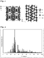
- Fig. 1 is a diagram showing a crystal structure of Ba 1 Si 7 N 10 crystal.
- (Ba, Sr) 1 (Si, Al) 7 (O, N) 10 :Li + is one of crystals having the same crystal structure as the Ba 1 Si 7 N 10 crystal, into which Li is solid-solved, and, according to the single crystal structure analysis performed with respect to the (Ba, Sr) 1 (Si, Al) 7 (O, N) 10 :Li + crystal, the (Ba, Sr) 1 (Si, Al) 7 (O, N) 10 :Li + crystal belongs to the monoclinic crystal system and the P c space group (space group No. 7 in the International Tables for Crystallography) and has crystal parameters and atomic coordinate positions as shown in Table 1.
- the expression of "inorganic crystal:metal element” is an expression to show material in which the metal element is solid-solved into the inorganic crystal such that the expression of (Ba, Sr) 1 (Si, Al) 7 (O, N) 10 :Li + indicates the material in which the monovalent Li is solid-solved into the (Ba, Sr) 1 (Si, Al) 7 (O, N) 10 crystal.
- (Ba, Sr) 1 (Si, Al) 7 (O, N) 10 :Li + was synthesized as follows.
- a mixture composition of silicon nitride (Si 3 N 4 ), alumun nitride (AlN), lithium nitride (Li 3 N), strontium nitride (Sr 3 N 2 ), and barium nitride (Ba 3 N 2 ) was designed to have 2:1:0.667:0.0667:0.2667 in the molar ratio, and the mixture powder was prepared by weighing and mixing raw materials to satisfy the mixture composition, and the mixed mixture powder was fired in similar processes as described later with respect to Example 1.
- lattice constants a, b, and c signify respective lengths of the axes of the unit cell
- ⁇ , ⁇ , and ⁇ signify respective angles between axes of the unit cell.
- the atomic coordinates indicate a position of each atom in the unit cell in terms of a value between 0 and 1 using the unit cell as a unit. According to the analysis results thus obtained, there were atoms of Ba, Sr, Si, Al, N, and O, respectively, and Ba and Sr existed in one kind of site: (Ba, Sr(1)) without distinguishing Ba site from Sr site.
- Si and Al occupied seven (7) kinds of sites: (Si, Al(1) to (Si, Al(7)) without distinguishing Si site from Al site. Further, according to the analysis results thus obtained, O and N occupied ten (10) kinds of sites: (O, N(1) to O, N(10)) without distinguishing O site from N site. Also, Li was detected by the ICP mass spectrometry measurement, but the position in the atomic coordinates could not be identified such that it is suggested that Li was solid-solved by the interstitial solid solution.
- the composition of (Ba,Sr) 1 (Si,Al) 7 (O,N) 10 :Li + crystal was represented by Ba 0.8 Sr 0.2 Si 6.7 Al 0.3 Li 0.1 O 0.2 N 9.8 .
- Table 1 Crystal structure data of (Ba,Sr)1(Si,Al)7(O,N)10: Li+ crystal Crystal composition (Ba,Sr)1(Si,Al)7(O,N)10: Li+ Formula weight (Z) 2 Crystal system Monoclinic Space group Pc Space group number 7 Lattice constants a 6.8875 ⁇ b 6.7102 ⁇ c 9.6756 ⁇ ⁇ 90 degree ⁇ 106.166 degree ⁇ 90 degree Atom Atomic coordinate Atomic coordinate x y z Site occupancy rate Ba,Sr(1) 0.010439 0.401545 0.225284 1 Si,Al(1) 0.430123 0.526341 0.069747 1 Si,Al(2) -0.389034 0.526843 0.38115 1 Si,Al(3) -0.140364 0.895103 0.324761 1 Si,Al(4) 0.119404 0.875815 0.091222 1 Si,Al(5) 0.303493 0.133782 -0.093851 1 Si,Al(6) -
- the (Ba,Sr) 1 (Si,Al) 7 (O,N) 10 :Li + crystal was found to have the structure as shown in Fig. 1 , in which a Ba element, a Sr element, and a Li element are included in a skeleton formed by linking tetrahedrons constituted of bonds of Si or Al with O or N.
- the M element to become an activating ion such as Eu is incorporated into the crystal in the type of partial substitution of the Ba element or the Sr element in the crystal.
- a 1 (D, E) 7 X 10 crystal As a crystal having a crystal structure identical to the crystal structure of (Ba,Sr) 1 (Si,Al) 7 (O,N) 10 :Li + crystal, which was synthesized and subjected to the structure analysis, there may be included A 1 (D, E) 7 X 10 crystal and, more specifically, A 1 (Si,Al) 7 (O,N) 10 crystal, into which Li is solid-solved.
- the A element is typically Sr or Ba or a mixture of Sr and Ba.
- A can occupy a site which Ba is supposed to occupy
- D and E can occupy a site which Si is supposed to occupy
- X can occupy a site which N is supposed to occupy in the Ba 1 Si 7 N 10 crystal.
- a relative ratio of numbers of atoms can be adjusted to one (1) for the element A, seven (7) for the sum of D and E, and ten (10) for the sum of X while the crystal structure remains the same.
- Si and Al can occupy a site which Si is supposed to occupy and O and N can occupy a site which N is supposed to occupy in the Ba 1 Si 7 N 10 crystal.
- a relative ratio of numbers of atoms can be adjusted to one (1) for the A element, seven (7) for the sum of Si and Ai, and ten (10) for the sum of O and N while the crystal structure remains the same.
- the Ba 1 Si 7 N 10 system crystal can generally be identified by means of the X-ray diffraction or the neutron diffraction.
- a substance exhibiting the identical diffraction to that of the Ba 1 Si 7 N 10 system crystal as a result of the X-ray diffraction in the present invention comprises a crystal represented by A 1 (D, E) 7 X 10 .
- a 1 (D, E) 7 X 10 the ranges of A, D, E, and X only for the following descriptions of the specification are definded in this and later paragraphs.
- A is one or two elements selected from the group consisting of Sr, and Ba; D is Si; E is Al; and X is N or a mixture of N and O.
- the Ba 1 Si 7 N 10 system crystal can be identified by means of the X-ray diffraction or the neutron diffraction.
- a substance exhibiting the identical diffraction to that of the Ba 1 Si 7 N 10 system crystal as a result of the X-ray diffraction in the present invention comprises a crystal represented by A 1 (D, E) 7 X 10 . Further, the substance comprises a crystal in which lattice constants or atomic positions are changed by substituting other elements for constituent elements in the Ba 1 Si 7 N 10 crystal.
- specific examples of materials in which the constituent elements are substituted with other elements comprise a material in which Ba in the Ba 1 Si 7 N 10 crystal is partially or completely substituted with the A element other than Ba (here, A is one or two or more kinds of elements selected from the group consisting of Mg, Ca, Sr, and Ba) or the M element (here, M is one or two or more kinds of elements selected from the group consisting of Mn, Ce, Pr, Nd, Sm, Eu, Tb, Dy, and Yb) .
- Si in the crystal is partially or completely substituted with the D element excluding Si
- D is one or two or more kinds of elements selected from the group consisting of Si, Ge, Sn, Ti, Zr, and Hf
- E is one or two or more kinds of elements selected from the group consisting of B, Al, Ga, In, Sc, Y, and La
- N in the crystal is partially or completely substituted with O or fluorine. These substitutions are performed such that the neutrality of charges in the whole crystal is maintained.
- the lattice constants change as the constituent components are substituted with other elements or as an activating element such as Eu is solid-solved therein, but the atomic positions given by the crystal structure, sites to be occupied by atoms, and coordinates thereof do not significantly change to an extent in which a chemical bond between skeleton atoms is broken.
- a crystal structure is defined to be identical to that of the Ba 1 Si 7 N 10 crystal if lengths of chemical bonds (distance of neighboring atoms) of Al-N and Si-N calculated from the lattice constants and atomic coordinates obtained by conducting Rietveld analysis of the results from the X-ray diffraction or the neutron diffraction in the space group of Pc are compared with lengths of chemical bonds calculated from the lattice constants and atomic coordinates of the Ba 1 Si 7 N 10 crystal as shown in Table 1 such that the difference between the lengths is within ⁇ 5%, and using the definition it is determined whether the crystal having the crystal structure belongs to the Ba 1 Si 7 N 10 system crystal or not.
- This determination criterion is employed herein since it was once observed that a crystal in the Ba 1 Si 7 N 10 system crystal was changed to become another crystal due to breakage of chemical bonds when lengths of the chemical bonds were changed beyond ⁇ 5% according to the prior experiments.
- a new substance can be identified to have the same crystal structure if main peaks of the resultant X-ray diffraction pattern measured with the new substance are respectively located at diffraction peak positions, which agree with the peak positions (2 ⁇ ) of the diffraction pattern calculated using the crystal structure data of Table 1 and the lattice constants calculated from the resultant X-ray diffraction pattern.
- Fig. 2 is a diagram showing a powder X-ray diffraction pattern using Cu K ⁇ -line calculated from the crystal structure of the (Ba, Sr) 1 (Si, Al) 7 (O, N) 10 :Li + crystal.
- a crystal structure of the Ba 1 Si 7 N 10 system crystal as an approximate structure using another crystal system of the monoclinic crystal and, in such a case, the crystal structure is expressed using a different space group, different lattice constants, and different plane indices, but the X-ray diffraction results (for example, Fig. 2 ) and the crystal structure (for example, Fig. 1 ) remain unchanged such that an identification method and an identification result thereof are the same. Therefore, in the present invention, it is to perform an X-ray diffraction analysis using the monoclinic crystal system.
- the method of identifying the substance based on Table 1 will be concretely described in Examples to be described later, and the explanation of the method described herein is just in general.
- a phosphor can be obtained if the Ba 1 Si 7 N 10 system crystal is activated by, as the M element, one or two or more kinds of elements selected from the group consisting of Mn, Ce, Pr, Nd, Sm, Eu, Tb, Dy, Ho, Er, Tm, and Yb. Since emission characteristics such as an excitation wavelength, an emission wavelength, and emission intensity may vary depending on the composition of the Ba 1 Si 7 N 10 system crystal, and the kind and quantity of the activating element, such conditions may be chosen in accordance with an application thereof.
- the phosphor represented by a composition formula of L c M d A e D f E g X h (here, in the formula, c+d+e+f+g+h 1, L is a Li element, M is one or two or more kinds of elements selected from the group consiting of Mn, Ce, Pr, Nd, Sm, Eu, Tb, Dy, and Yb; A is one or two or more kinds of elements selected from the group consiting of Mg, Ca, Sr, and Ba; D is one or two or more kinds of elements selected from the group consiting of Si, Ge, Sn, Ti, Zr, and Hf; E is one or two or more kinds of elements selected from the group consiting of B, Al, Ga, In, Sc, Y, and La; and X is one or two or more kinds of elements selected from the group consiting of O, N, and F) and having the parameters c, d, e, f, g, and h satisfy all conditions: 0.001
- the parameter c is a parameter representing a constituent amount of the L element such as Li, and if the amount is less than 0.001 or higher than 0.7, the crystal structure becomes unstable so as to cause the emission intensity to decrease.
- the parameter d represents an additive amount of the activating element, and if the amount is less than 0.00001, an amount of light-emitting ions is insufficient so as to cause brightness to decrease. If the amount is more than 0.05, the emission intensity may be decreased due to the concentration quenching by a mutual interaction between light-emitting ions.
- the parameter e is a parameter representing a constituent amount of the alkaline earth element such as Ba, and if the amount is less than 0.01 or higher than 0.1, the crystal structure becomes unstable so as to cause the emission intensity to decrease.
- the parameter f is a parameter representing a constituent amount of the D element such as Si, and if the amount is less than 0.1 or higher than 0.4, the crystal structure becomes unstable so as to cause the emission intensity to decrease.
- the parameter g is a parameter representing a constituent amount of the E element such as Al, and if the amount is higher than 0.1, the crystal structure becomes unstable so as to cause the emission intensity to decrease.
- the parameter g is greater than zero (0) .
- the parameter h is a parameter representing a constituent amount of the X element such as O, N, and F, and if the amount is less than 0.15 or higher than 0.65, the crystal structure becomes unstable so as to cause the emission intensity to decrease.
- the element X is an anion, and the composition ratio of O, N, and F is determined in order to maintain the charge neutrality with a cation of the A, M, D and E elements.
- the crystal having the composition in which the parameters f and g satisfy the condition: 0.8 ⁇ f / f + g ⁇ 1.0 , is stable in the crystal structure and exhibits high emission intensity.
- the inorganic crystal having the composition, in which the X element comprises N and O and the ratio of h1 and h2 (here, h1+h2 h), which are numbers of N atoms and O atoms contained in the inorganic compound, respectively, satisfies the condition of 0 / 10 ⁇ h 2 / h 2 + h 1 ⁇ 2 / 10 , is stable in the crystal structure and exhibits high emission intensity.
- it is the phosphor that is easy to make a material design since an excitation wavelength thereof or an emission wavelength thereof can be continuously changed by utilizing this feature.
- a phosphor in which an inorganic compound includes single crystal particles or an aggregate of the single crystal particles having a mean particle diameter of 0.1 ⁇ m or more and 100 ⁇ m or less has high emission efficiency and a good handling property when it is applied to an LED such that it is good to control the particle diameter thereof in this range.
- Impurity elements of Fe, Co, and Ni included in the inorganic compound may cause the emission intensity to decrease. If the sum of these impurity elements in the phosphor is controlled to be 500 ppm or less, an influence of these elements on the emission intensity is decreased.
- the phosphor of the present invention may further comprise an amorphous phase or another crystal phase in addition to the inorganic compound, in which the Li element and the M element are solid-solved into the above-described Ba 1 Si 7 N 10 system crystal as the host crystal, and the content amount of the above-mentioned inorganic compound is equal to or more than 20 mass%.
- the present embodiment may be employed.
- the content amount of the above-mentioned inorganic compound may be adjusted in accordance with the target property, but the emission intensity could be lowered if the amount is less than 20 mass%.
- the amount of the main component is equal to or more than 20 mass%.
- an inorganic substance having electrical conductivity may be added thereto as another crystal phase or an amorphous phase.
- oxide As the inorganic substance having the electrical conductivity, oxide; oxynitride; or nitride of one or two or more kinds of elements selected from the group consisting of Zn, Al, Ga, In, and Sn, or a mixture of any of these may be named.
- Zn Zn
- Al Al
- Ga In
- Sn Sn
- zinc oxide, aluminum nitride, indium nitride, tin oxide, and so on may be named.
- a second phosphor may be added thereto.
- a BAM phosphor, a ⁇ -sialon phosphor, an ⁇ -sialon phosphor, a (Sr, Ba) 2 Si 5 N 8 phosphor, a CaAlSiN 3 phosphor, and a (Ca, Sr)AlSiN 3 phosphor may be named.
- These inorganic phosphors may be utilized as the above-described other crystal phase or amorphous phase.
- a phosphor having a peak at a wavelength in the range of 470 nm to 620 nm upon irradiation by an excitation source there is a phosphor having a peak at a wavelength in the range of 470 nm to 620 nm upon irradiation by an excitation source.
- a phosphor of the B ai Si 7 N 10 system crystal in which Eu is activated has an emission peak in this range by adjusting the composition.
- the excitation source comprising vacuum ultraviolet light, ultraviolet light, or visible light having a wavelength of 100 nm or more to 450 nm or less, or electron beam or X-ray.
- the phosphor can be made to emit light efficiently by using such excitation sources.
- a phosphor comprising, as the main component, an inorganic compound comprising a crystal represented by A 1 (D,E) 7 X 10 or an inorganic crystal having the same crystal structure as the crystal represented by Ba 1 Si 7 N 10 , into which Li and Eu are solid-solved. Since the phosphor emits white color fluorescence of at least 470 nm and not exceeding 620 nm by adjusting the composition upon irraditation of light from 100 nm to 410 nm, the phosphor is desiable for use in a white color emission application such as a white color LED.
- a phosphor upon irradiation by the excitation source, to emit light of a specific color which satisfies, in terms of values of (x, y) of CIE 1931 chromaticity coordinates, conditions: 0.25 ⁇ x ⁇ 0.45 ; and 0.25 ⁇ y ⁇ 0.45.
- the phosphor may be applied for the white color emission of the white color LED and the like.
- the phosphor may be preferably applied for white color emission of the white color LED or the like.
- the phosphor of the present invention is characterized by having a wider excitation range of an electron beam and X-ray and light from ultraviolet light to visible light, emitting light of white color, and, in particular, both emitting light of a white color from 470 nm to 620 nm with a specific composition thereof and being capable of adjusting an emission wavelength and an emission peak width.
- the phosphor of the present invention is suitable for an illuminating device, an image display device, pigment, and an ultraviolet absorber because of such emission characteristics.
- the phosphor of the present invention has also advantages of excellent heat resistance since it does not degrade even if it is exposed to a high temperature, and has excellent long-term stability under an oxidizing atmosphere and a moisture environment, such that a product having excellent durability can be provided by utilizing the phosphor.
- a method of manufacturing such a phosphor of the present invention is not particularly limited, but, for example, a mixture of metal compounds being a raw material mixture that can constitute the phosphor of the Ba 1 Si 7 N 10 system crystal is fired in a nitrogen-containing inert atmosphere in the temperature range of 1,200 °C or higher to 2,200 °C or lower so as to obtain the phosphor of the present invetion.
- the main crystal of the present invention belongs to the monoclinic system and the space group P c
- another crystal that belongs to another crystal system and another space group other than the above may be occasionally mixed therein depending on synthesis conditions such as firing temperature.
- a change of the emission characteristics is slight and therefore the thus-obtained product can be used to render high brightness emission.
- a mixture of metal compounds may comprise: a compound including Li, a compound including M, a compound including A, a compound including D, a compound including E if necessary, and a compound including X,
- M is one or two or more kinds of elements selected from a group consisting of Mn, Ce, Pr, Nd, Sm, Eu, Tb, Dy, and Yb
- A is one or two or more kinds of elements selected from a group consisting of Mg, Ca, Sr, and Ba
- D is one or two or more kinds of elements selected from a group consisting of Si, Ge, Sn, Ti, Zr, and Hf
- E is one or two or more kinds of elements selected from a group consisting of B, Al, Ga, In, Sc, Y, and La
- X is one or two or more kinds of elements selected from a group consisting of O, N, and F).
- the mixture which comprises the compound including M that is a single substance or a mixture of at least two kinds of substances selected from metal, silicide, oxide, carbonate, nitride, oxynitride, chloride, fluoride, or oxyfluoride including M; the compound including A that is a single substance or a mixture of at least two kinds of substances selected from metal, silicide, oxide, carbonate, nitride, oxynitride, chloride, fluoride, or oxyfluoride including A; and the compound including D that is a single substance or a mixture of at least two kinds of substances selected from a metal, silicide, oxide, carbonate, nitride, oxynitride, chloride, fluoride or oxyfluoride including D, is preferable because these raw materials are easily available and have excellent stability.
- the compound including X is a single substance or a mixture of at least two kinds of substances selected from the group consisting of X-containing oxide, nitride, oxynitride, fluoride, and oxyfluoride, it is preferable since the raw material is easily available and has excellent stability.
- the compound including E is a single substance or a mixture of at least two kinds of substances selected from the group consisting of E-containing metal, silicide, oxide, carbonate, nitride, oxynitride, chloride, fluoride, and oxyfluoride, it is preferable since the raw material is easily available and has excellent stability.
- the compound including Li is a single substance or a mixture of at least two kinds of substances selected from the group consisting of Li-containing metal, nitride of Li, oxide of Li, chrolide of Li, and fluoride of Li, it is desirable since the raw material is easily available and has excellent stability.
- a starting material comprising, at least, nitride or oxide of europium; nitride, oxide, or carbonate of barium; silicon oxide or silicon nitride; and nitride of Li since the reaction tends to easily proceed during the firing.
- the firing temperature is high and the firing atmosphere is an inert atmosphere containing nitrogen
- the nitrogen-containing inert atmosphere in the pressure range of 0.1 MPa or more to 100 MPa or less is preferable because thermal decomposition of nitride or oxynitride of the starting material or the product is suppressed.
- the oxygen partial pressure is 0.0001% or lower in the firing atmosphere in order to suppress the oxidation reaction of nitride or oxynitride of the starting material or the product.
- the firing time is, although it differs depending on the firing temperature, usually 1 to 10 hours or so.
- a material suitably includes a boron nitride coated container, which is exemplified by a boron nitride coated graphite crucible used for synthesis of an ⁇ -sialon as described in a scientific journal " Journal of the American Ceramic Society” Vol. 85, No. 5, pages 1229 to 1234 in 2002 , or boron nitride sintered body.
- boron or boron nitride component is mixed into the product from the container, but, if the amount thereof is small, an effect of mixing is slight since the emission characteristics are not deteriorated. Further, durability of the product may be occasionally improved by the addition of a small amount of boron nitride thereto, and such addition may be preferable in some cases.
- the term relative bulk density means the ratio of a value (bulk density) given by dividing the mass of powder material filled in the container by the capacity of the container to the real density of the substance of the powder material. Unless otherwise noted in the present specification, the relative bulk density is referred to as simply the bulk density.
- the mean particle diameter of powder particles or aggregate of the raw material equal to or less than 500 ⁇ m since the raw material has excellent reactivity and handling characteristics.
- a particle size of the particles or aggregates As a method of adjusting a particle size of the particles or aggregates to be 500 ⁇ m or less, it is preferable to employ a spray dryer, sieving, or pneumatic classification since such a method has excellent operating efficiency and handling characteristics.
- a method of firing not the hot-pressing, but a method of firing, in which no external mechanical pressing is applied, such as pressureless sintering method and gas pressure sintering method is preferable as a method of obtaining a product of powder or aggregate.
- a mean particle diameter of the phosphor powder is preferably 50 nm or more and 200 ⁇ m or less in terms of a volume-based median diameter (d50) because the emission intensity is high.
- the volume-based mean particle diameter can be measured, for example, by a Microtrac or a laser light scattering method.
- a mean particle diameter of phosphor powder synthesized by firing may be satisfactorily adjusted to be at least 50 nm and not exceeding 200 ⁇ m by applying at least one technique selected from pulverization, classification, and acid treatment.
- Defects included in the powder and damages caused by pulverization may be occasionally cured by heat-treating the phosphor powder after firing, the phosphor powder after pulverizing treatment, or the phosphor powder after controlling a particle size at a temperature of 1,000°C or higher to the firing temperature or lower.
- the defects and damages may occasionally cause a decrease in the emission intensity, and in such a case, the emission intensity may be recovered by the heat treatment.
- a stable crystal may be occasionally obtained by adding an inorganic compound forming a liquid phase at a temperature of a firing temperature or lower and firing a mixture thereof such that the liquid phase acts as a flux to promote the reaction and particle growth, and thus the emission intensity may be occasionally improved.
- the inorganic compound forming the liquid phase at the temperature of the firing temperature or lower include a single substance or a mixture of two or more kinds of fluoride, chloride, iodide, bromide, or phosphate of one or two or more kinds of elements selected from the group consiting of Li, Na, K, Mg, Ca, Sr, and Ba.
- the inorganic compounds have different melting points, respectively, and therefore may be satisfactorily used properly depending on a synthesizing temperature.
- the emission intensity of the phosphor of the present invention may occasionally become high by reducing the content amount of the inorganic compound forming the liquid phase at the temperature of the firing temperature or lower by washing the phosphor with a solvent after the firing.
- the phosphor of the present invention When the phosphor of the present invention is used in an application of a light-emitting device or the like, it is preferable to use the phosphor dispersed in a liquid medium. And the phosphor can be used as the phosphor mixture including the phosphor of the present invention.
- a composition prepared by dispersing the phosphor of the present invention in the liquid medium is referred to as a phosphor-containing composition.
- any liquid medium can be selected depending on a purpose or the like, if the liquid medium shows liquid properties under desired use conditions to suitably disperse the phosphor of the present invention, and simultaneously does not cause an undesirable reaction or the like.
- an addition reaction type silicone resin and a condensation reaction type silicone resin before curing a modified silicone resin, an epoxy resin, a polyvinyl resin, a polyethylene resin, a polypropylene resin, a polyester resin, and so on are named.
- a single kind of liquid medium may be used by itself, or any combination of two or more kinds of liquid media with any combination ratio thereof may be used.
- An amount of used liquid medium or media may be appropriately adjusted depending on an application or the like.
- the amount is in the range of generally 3 wt% or more and preferably 5 wt% or more, to generally 30 wt% or less and preferably 15 wt% or less in terms of the weight ratio of the liquid medium to the phosphor of the present invention.
- the phosphor-containing composition of the present invention may contain, in addition to the phosphor of the present invention and the liquid medium, any other component depending on an application or the like.
- a dispersing agent, a thickening agent, an extending agent, a buffering agent, and so on are named.
- silica fine powder such as Aerosil, alumina, and so on may be named.
- the light-emitting device of the present invention is configured by using at least an excitation light-emitting body or an emission source, and the phosphor of the present invention.
- the excitation light-emitting body or the emission source there are an LED light-emitting device, a laser diode light-emitting device, an electroluminescence (EL) light-emitting device, a fluorescent lamp, and so on.
- the LED light-emitting device can be manufactured using the phosphor of the present invention and by a publicly known method which is described in Japanese Patent Application Publication No. H05 (1993) -152609 , Japanese Patent Application Publication No. H07 (1995) -99345 , Japanese Patent No. 2927279 , or the like.
- the light-emitting body or the emission source is preferably what emits light of a wavelength from 330 to 500 nm.
- an LED light-emitting element emitting an ultraviolet (or violet) ray of a wavelength from 330 to 420 nm, or an LED light-emitting element emitting blue light in a wavelength from 420 to 500 nm is preferable.
- Such LED light-emitting elements include a nitride semiconductor such as GaN or InGaN, which can be an emission source of a predetermined wavelength by adjusting the composition.
- a white color light-emitting diode As a light-emitting device of the present invention, there are a white color light-emitting diode, an illuminating device including a plurality of white color light-emitting diodes or a backlight for a liquid crystal panel, and the like, which include the phosphor of the present invention, respectively.
- the device may further include one or two or more kinds of phosphor selected from ⁇ -sialon phosphor activated with Eu, ⁇ -sialon yellow phosphor activated with Eu, Sr 2 Si 5 N 8 orange phosphor activated with Eu, (Ca, Sr)AlSiN 3 orange phosphor activated with Eu, and CaAlSiN 3 red phosphor activated with Eu.
- ⁇ -sialon phosphor activated with Eu ⁇ -sialon yellow phosphor activated with Eu
- Sr 2 Si 5 N 8 orange phosphor activated with Eu Sr 2 Si 5 N 8 orange phosphor activated with Eu
- (Ca, Sr)AlSiN 3 orange phosphor activated with Eu and CaAlSiN 3 red phosphor activated with Eu.
- the yellow phosphor other than the above, for example, YAG:Ce, (Ca, Sr, Ba)Si 2 O 2 N 2 :Eu, and the like may be
- the light-emitting device of the present invention there is a light-emitting device to emit light having chromaticity where the values of (x, y) of CIE 1931 chromaticity coordinates, which are emitted by the phosphor of the present invention, are in the ranges of: 0.25 ⁇ x ⁇ 0.45 and 0.25 ⁇ y ⁇ 0.45 while the excitation light-emitting body or the emission source emits ultraviolet or visible light having a peak wavelength of 300 to 410 nm.
- a blue color phosphor emitting light having a peak wavelength of 450 nm to 500 nm or less by means of the excitation light-emitting body or the emission source can further be included.
- a blue phosphor there are AlN: (Eu, Si), BaMgAl 10 O 17 :Eu, SrSi 9 Al 19 O 31 :Eu, LaSi 9 Al 19 N 32 :Eu, ⁇ -sialon:Ce, JEM:Ce, and so on.
- the expression of "inorganic crystal:metal element” is an expression to show material in which the metal element is solid-solved into the inorganic crystal such that the expression of AlN: (Eu, Si) indicates the material in which Eu and Si are solid-solved into the AlN crystal.
- a green phosphor emitting light having a peak wavelength of at least 500 nm and not exceeding 550 nm by means of the light-emitting body or the emission source can further be included.
- a green phosphor there are ⁇ -sialon:Eu, (Ba, Sr, Ca, Mg) 2 SiO 4 :Eu, (Ca, Sr, Ba)Si 2 O 2 N 2 :Eu, and so on.
- a yellow phosphor emitting light having a peak wavelength of at least 550 nm and not exceeding 600 nm by means of the light-emitting body or the emission source can further be included.
- a yellow phosphor include YAG:Ce, ⁇ -sialon:Eu, CaAlSiN 3 :Ce, La 3 Si 6 N 11 :Ce, and so on.
- a red phosphor emitting light having a peak wavelength of at least 600 nm and not exceeding 700 nm by means of the light-emitting body or the emission source can further be included.
- a red phosphor there are CaAlSiN 3 :Eu, (Ca, Sr)AlSiN 3 :Eu, Ca 2 Si 5 N 8 :Eu, Sr 2 Si 5 N 8 :Eu, and so on.
- a light-emitting device with high efficiency can be configured since the emission efficiency is high if an LED in which the light-emitting body or the emission source emits light having a wavelength of 300 to 410 nm is used.
- the light-emitting device of the present invention there is a light-emitting device having a short wavelength light absorbing material to absorb light of 410 nm or less and to tansmit light of 420 nm or more.
- the image display device of the present invention is constituted of at least an excitation source and the phosphor of the present invention and includes a fluorescent display tube (VFD), a field emission display (FED), a plasma display panel (PDP), a cathode-ray tube (CRT), and the like. It has been confirmed that the phosphor of the present invention emits light by excitation of a vacuum ultraviolet ray of 100 to 190 nm, an ultraviolet ray of 190 to 380 nm, an electron beam, or the like, and the above image display devices can be configured by combining these excitation sources and the phosphors of the present invention.
- VFD fluorescent display tube
- FED field emission display
- PDP plasma display panel
- CRT cathode-ray tube
- the phosphor comprising an inorganic compound crystal phase having a specific chemical composition according to the present invention has a white color as an object color, and thus can be used as a pigment or fluorescent pigment. That is, the object color of white is observed when the phosphor of the present invention is irradiated with sunlight or light from a fluorescent lamp or the like.
- the phosphor of the present invention is suitable for an inorganic pigment. Therefore, when the phosphor of the present invention is used for a paint, ink, color, glaze, colorant to be added to a plastic product or the like, a favorable coloring can be maintained at a high level for a long period of time.
- the phosphor of the present invention absorbs ultraviolet ray so as to be suitable also as the ultraviolet absorber.
- a shielding effect thereof against the ultraviolet ray is so high that the product may be effectively protected from the ultraviolet degradation.
- the raw material powders used for the synthesis were: silicon nitride powder with a particle size of specific surface area of 11.2 m 2 /g, oxygen content of 1.29 wt%, and ⁇ type content of 95% (SN-E10 grade; made by Ube Industries, Ltd.); aluminum nitride powder with a particle size of specific surface area of 3.3 m 2 /g and oxygen content of 0.82 wt% (E grade made by Tokuyama Corporation); lithium nitride (made by Kojundo Chemical Laboratory Co., Ltd.); strontium nitride of 99.5% purity (Sr 3 N 2 ; made by Materion Advanced Chemicals); barium nitride of 99.5% purity (Ba 3 N 2 ; made by Materion Advanced Chemicals); celium nitride (CeN; manufactured by nitriding by heating metal cerium in the nitrogen flow at 600 °C); and europium nitride (EuN; synthesized by heating metal europium in the
- Silicon nitride (Si 3 N 4 ); aluminum nitride (AlN) ; lithium nitride (Li 3 N); strontium nitride (Sr 3 N 2 ); barium nitride (Ba 3 N 2 ) , and europium nitride (EuN) were mixed in the molar ratio of 2.33:1:0.667:0.5:0.133:0.1 such that a mixture composition thereof was designed.
- the crucible containing the powder mixture was set into an electric furnace of a graphite resistance heating type.
- the firing atmosphere was made vacuum of 1x10 -1 Pa or less with a diffusion pump, and heated from the room temperature to 800 °C at a rate of 500 °C per hour.
- Nitrogen of 99.999 vol% purity was introduced at 800 °C to raise the pressure inside the furnace to 1 MPa, and the temperature was further raised to 1,900 °C at a rate of 500 °C per hour, and then the temperature was maintained for two (2) hours.
- the synthesized compound was observed with the microscope to find the synthesized compound was a mixture including a single crystal and other phases. From the synthesized compound, a single crystal particle having a size of 49 ⁇ m X 65 ⁇ m X 97 ⁇ m was picked up. The crystal particle was analyzed using a scanning electron microscope (SEM; SU1510 made by Hitachi High-Technologies Corp.) equipped with an energy dispersive elemental analyzer (EDS; QUANTAX made by Bruker AXS Inc.) so as to perform the elemental analysis for the elements included in the crystal particle. As a result, presence of Ba, Sr, Si, Al, Eu, O, and N elements was confirmed. Here, it is plausible that the detected O element was caused by a micro amount of oxygen contained in the raw material powders.
- SEM scanning electron microscope
- EDS energy dispersive elemental analyzer
- the crystal was fixed to a tip top of a glass fiber with an organic adhesive.
- An X-ray diffraction measurement of the crystal was performed under a condition in which an output of an X-ray source was 50 kV and 50 mA using a single crystal X-ray diffractometer with a rotating target of Mo K ⁇ -line (SMART APEX II Ultra made by Bruker AXS Inc.).
- SMART APEX II Ultra made by Bruker AXS Inc.
- the crystal structure was determined using a single crystal structure analysis software (APEX2 made by Bruker AXS Inc.) from the results of X-ray diffraction measurement.
- APEX2 made by Bruker AXS Inc.
- the thus-obtained crystal structure data and the crystal structure are consistent to those of Table 1 and Fig. 1 , respectively.
- the Li in the crystal was analyzed by the ICP mass spectrometry equipped with a Laser ablation.
- the sample was irradiated with laser light of the wavelenth of 213 nm with a beam diameter of 30 ⁇ m emitted by the Nd:YAG laser made by New Wave Research, Inc. and the Li element sublimated from the sample was analyzed by the ICP mass spectrometer. As a result, it was confirmed that the sample contained Li.
- the crystal obtained from the ratio of Li:Ba:Sr:Si:Al:Eu based on the measured values of the EDS and the ICP and the crystal structure data was (Ba, Sr, Eu) 1 Si 6.7 Al 0.3 Li 0.1 O 0.2 N 9.8 , and a sinble crystal in which Li was solid-solved into (Ba, Sr, Eu) 1 (Si, Al) 7 (O, N) 10 as one of the crystals having the same crystal structure as the Ba 1 Si 7 N 10 crystal.
- the reason why the composition of the starting raw material differed from the crystal composition is that a small amount of another composition other than (Ba, Sr, Eu) 1 Si 6.7 Al 0.3 Li 0.1 O 0.2 N 9.8 was generated as the second phase, but the present measurement was conducted with the single crystal such that the analysis result indicates the pure (Ba,Sr,Eu) 1 Si 6.7 Al 0.3 Li 0.1 O 0.2 N 9.8 structure.
- Fig. 3 is a diagram showing an emission spectrum of (Ba, Sr, Eu) 1 (Si, Al) 7 (O, N) 10 :Li + single crystal particle.
- the Ba 1 Si 7 N 10 crystal was found to allow Sr to substitute partially or entirely Ba while the crystal structure remains the same. That is, the crystal of A 1 Si 7 N 10 (A is one or two kinds of elements selected from Ba, Sr, or a mixture thereof) has the same crystal structure as the Ba 1 Si 7 N 10 crystal. Further, with respect to this crystal, it was confirmed that Al could substitute partially Si and oxygen could substitute partially N, and that the crystal was one of the compositions of the crystal groups having the crystal structure identical to that of Ba 1 Si 7 N 10 .
- the crucible containing the powder mixture was set into an electric furnace of a graphite resistance heating type.
- the firing conditions are shown in Table 5.
- the firing atmosphere was made vacuum of 1x10 -1 Pa or less with a diffusion pump, and heated from the room temperature to 800 °C at a rate of 500 °C per hour.
- Nitrogen of 99.999 vol% purity was introduced at 800 °C to raise the pressure inside the furnace to 1 MPa, and the temperature was further raised to the predetermined temperature at a rate of 500 °C per hour, and then the temperature was maintained for the predetermined time.
- Example 2 Design compositions (atomic ratios) in examples and comparative example
- Example M element L element A element D element E element X element Li Sr Ba Si Al N
- Comparative example 1 Eu 0.02 0.98 7 10
- Example 2 Eu 0.2 3 0.8 6.4 0.6 10
- Example 3 Eu 0.2 9 0.8 6.4 0.6 13
- Example 4 Ce 0.1 9 0.9 6.4 0.6 13
- Example 5 Eu, Ce 0.2 9 0.8 6.4 0.6 13
- Example 6 Eu 0.2 3 0.8 6.4 0.6 10
- Example 7 Eu 0.2 9 0.8 6.4 0.6 13
- Example 8 Eu 0.2 30 0.8 5.8 1.2 20
- Example 10 Eu, Ce 0.2 9 0.8 6.4 0.6 13
- Example 11 Ce 0.2 9 0.8 6.4 0.6 13
- Example 12 Eu 0.1 2 0.95 0.95 7 1 12
- Example 13 Eu 0.1 2 1.5 0.4 7 1 12
- Example 14 Eu 0.05 0.8 0.95 6.3 0.7 10
- Table 3 Design compositions (parameters) in examples and comparative example
- Comparative example 1 Eu 0.001111 0.054444 0.388889 0.555556
- Example 2 Eu 0.009524 0.142857 0.038095 0.304762 0.028571 0.47619
- Example 3 Eu 0.006667 0.3 0.026667 0.213333 0.02 0.433333
- Example 4 Ce 0.003333 0.3 0.03 0.213333 0.02 0.433333
- Example 6 Eu 0.009524 0.142857 0.038095 0.304762 0.028571 0.47619
- Example 7 Eu 0.006667 0.3 0.026667 0.213333 0.02 0.433333
- Example 8 Eu 0.003448 0.517241 0.013793 0.1 0.02069 0.344828
- Example 9 Ce 0.003333
- Table 5 Firing conditions in examples and comparative example Example Firing conditions Temperature (°C) Ambient pressure (Mpa) Time (hour) Comparative example 1 1900 1 2 Example 2 1800 1 2 Example 3 1800 1 2 Example 4 1800 1 2 Example 5 1800 1 2 Example 6 1900 1 2 Example 7 1900 1 2 Example 8 1900 1 2 Example 9 1900 1 2 Example 10 1900 1 2 Example 11 1900 1 2 Example 12 1800 1 2 Example 13 1800 1 2 Example 14 1700 1 2
- each synthesized compound was ground using an agate mortar and the powder X-ray diffraction measurement using Cu K ⁇ -line was carried out.
- Main formation phases are shown in Table 6.
- the synthesized material included a rare earth element, an alkaline earth metal, Si, and N, and further included Al and O in some cases by the measurement of EDS.
- the presence of Li was confirmed by the laser ablation ICP mass spectrometry measurement.
- the synthesized material was a phosphor including an inorganic compound in which Li and M as the light-emitting ion such as Eu were solid-solved into the crystal having the same crystal structure as the Ba 1 Si 7 N 10 crystal.
- Table 6 Main formation phases in examples and comparative example Example Main formation phases Main phase Comparative example 1 Crystal structure identical to that of Table 1 Example 2 Crystal structure identical to that of Table 1 Example 3 Crystal structure identical to that of Table 1 Example 4 Crystal structure identical to that of Table 1 Example 5 Crystal structure identical to that of Table 1 Example 6 Crystal structure identical to that of Table 1 Example 7 Crystal structure identical to that of Table 1 Example 8 Crystal structure identical to that of Table 1 Example 9 Crystal structure identical to that of Table 1 Example 10 Crystal structure identical to that of Table 1 Example 11 Crystal structure identical to that of Table 1 Example 12 Crystal structure identical to that of Table 1 Example 13 Crystal structure identical to that of Table 1 Example 14 Crystal structure identical to that of Table 1
- the obtained firing products were crushed coarsely and further ground by hand using a crucible and mortar made of silicon nitride sintered body, and then allowed to pass a 30 ⁇ m-mesh sieve.
- the mean particle diameter was 3 to 8 ⁇ m.
- Example Emission characteristics and chromaticity in examples and comparative example Example Emission peak wavelength (nm) Emission intensity (arbitrary unit) Chromaticity x y Comparative example 1 479 0.48 0.16 0.27
- Example 2 555 0.97 0.37 0.43
- Example 3 558 0.25 0.38 0.44
- Example 4 551 0.81 0.33 0.39
- Example 5 543 0.81 0.34 0.41
- Example 6 560 0.81 0.4 0.45
- Example 7 564 0.56 0.4 0.45
- Example 8 564 0.96 0.4 0.46
- Example 9 525 0.9 0.32 0.38
- Example 10 555 0.88 0.38 0.45
- Example 11 532 0.96 0.31 0.38
- Example 12 566 0.95 0.38 0.44
- Example 13 596 0.83 0.38 0.4
- Example 14 480 0.5 0.32 0.37
- a portion in which a raw material mixture composition and a chemical composition of the synthesized compound show discrepancy has a trace amount of substance mixed in the synthesized product as an impurity secondary phase.
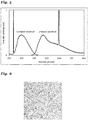
- Fig. 4 is a diagram showing a resultant powder X-ray diffraction pattern of a phosphor synthesized in Example 14.
- Fig. 5 is a diagram showing an excitation spectrum and an emission spectrum of the phosphor powder synthesized in Example 14.
- Example 14 The results of powder X-ray diffraction of the synthesized phosphors ( Fig. 4 ) show a good agreement with the results of structure analysis ( Fig. 2 ).
- the measured X-ray diffraction pattern is the same as the Ba 1 Si 7 N 10 crystal, and the crystal having the same crystal structure as the Ba 1 Si 7 N 10 crystal was confirmed to be the main component.
- the synthesized material was confirmed to include Li, Eu, Ba, Si, Al and N from the measurements of the laser ablation ICP mass spectrometry and the EDS. It was also confirmed that the ratio of (Ba+Eu) : (Si+Al) was 1:7.
- the synthesized material was confirmed to be a phosphor comprising an inorganic compound as the main component in which Li and Eu were solid-solved into the Ba 1 Si 7 N 10 system crystal.
- the phosphor was found to allow excitation at 298 nm most efficiently, and the emission spectrum was found to emit light having a peak at 472 nm when the phosphor was excited by light of 298 nm. Further, an emission color of the phosphor of Example 14 was confirmed to be within the following range: 0.25 ⁇ x ⁇ 0.45 ; and 0.25 ⁇ y ⁇ 0.45 in the CIE 1931 chromaticity coordinates.
- Fig. 6 is a diagram showing an object color of a phosphor synthesized in Example 14. Here, the diagram is shown in black and white due to the regulation of the application documents, but the original picture is in color and the color figure is readily submitted upon request.
- Example 14 it was confirmed that the synthesized compound obtained in Example 14 had a white color as an object color and was excellent in the coloration. Although not shown in the figure, synthesized compounds of other Examples also exhibited similar object color. It was understood that the synthesized compound of the present invention could be used as the pigment or the fluorescent pigment.
- Fig. 7 is a schematic diagram showing an illuminating device (bullet-type of LED illuminating device) according to the present invention.
- a so-called bullet-type white light-emitting diode lamp (1) shown in Fig. 7 was produced.
- the lower electrode of the ultraviolet light-emitting diode element (4) and the bottom surface of the recess are electrically connected with conductive paste, and the upper electrode and the other lead wire (3) are electrically connected through a gold thin wire (5).
- the phosphor (7) is dispersed in resin and mounted in the vicinity of the light-emitting diode element (4).
- the first resin (6) in which this phosphor is dispersed is transparent, and covers the entire ultraviolet light-emitting diode element (4).
- the tip-top portion of the lead wire including the recess, the blue light-emitting diode element, and the first resin in which the phosphor is dispersed are sealed with transparent second resin (8).
- a second resin (8) which is transparent is formed approximately in a cylindrical shape as a whole and the top portion is rounded in a lens shape such that the lamp is generally referred to as a bullet-type.
- the phosphor synthesized in Example 14 in a powder state and emitting light of white color (hereinafter referred to as simply white color phosphor for the phosphor in Example 14) was blended with epoxy resin by the concentration of 37 wt%, and an appropriate amount of blended mixture was dropped with a dispenser, and the mixture (7) in which the phosphor was blended was dispersed in the first resin (6) so as to be formed.
- Fig. 8 is a schematic diagram showing an illuminating device (board-mounting-type LED illuminating device) according to the present invention.
- a chip-type white light-emitting diode lamp (11) for board-mounting as shown in Fig. 8 was produced.
- Two lead wires (12, 13) are fixed to a white alumina ceramic board (19) having high reflectance of visible light and one end of each of the wires is located at approximately the center portion of the board and the other end of each of the wires extends outside to serve as an electrode to be soldered when the lamp is mounted on the electric board.
- One of the lead wires (12) has the one end on which an blue light-emitting diode element (14) having an emission peak wavelength of 450 nm is placed and fixed thereto such that the element is located at the center of the board.
- the lower electrode of the blue light-emitting diode element (14) and the lead wire below are electrically connected with conductive paste, and the upper electrode and the other lead wire (13) are electrically connected to a gold thin wire (15) .
- the first resin (16) and a white color phosphor (17) synthesized in Example 14 are mounted in the vicinity of the light-emitting diode device.
- the first resin in which this phosphor is dispersed is transparent, and covers the entire blue color light-emitting diode element (14).
- a wall surface member (20) having a hole opened at the center portion is fixed to the ceramic board.
- the wall surface member (20) has the center portion formed as the hole in which the blue color light-emitting diode element (14) and the resin (16) having the phosphor (17) dispersed therein are contained and the portion of the hole facing the center is made to be a slope.
- This slope is a reflective surface for taking out light forward, and the shape of the curved surface of the slope is determined in consideration of the direction of light reflection. Further, at least the surface which constitutes the reflective surface forms a surface having high visible light reflectance with white color or metallic luster.
- the wall surface member (20) is configured with white silicone resin.
- the hole at the center portion of the wall surface member is formed with a recess as the final shape of the chip-type light- emitting diode lamp, and is filled up with second transparent resin (18) to seal all of the blue light-emitting diode element (14) and the first resin (16) in which the phosphor (17) is dispersed.
- the same epoxy resin was used for both the first resin (16) and second resin (18).
- the percentage of phosphor addition, the attained chromaticity, and the like are approximately identical to those in Example 15.
- Fig. 9 is a schematic diagram showing an image display device (plasma display panel) according to the present invention.
- a red phosphor (CaAlSiN 3 :Eu 2+ ), a green phosphor ( ⁇ -sialon:Eu 2+ ), a blue phosphor (BAM:Eu 2+ ), and a white phosphor of Example 14 of the present invention are applied to inner surfaces of the respective cells (35, 36, 37, 38), which are arranged via electrodes (39, 40, 41, 42) and a dielectric layer (44) over a glass substrate (47).
- a vacuum ultraviolet ray is generated by Xe discharge in each of the cells, thereby exciting the respective phosphors so as to emit visible light of a red color, a green color, a blue color and a white color such that the emitted light may be observed from the outside through a protective layer (46), a dielectric layer (45), and a glass substrate (48) so as to serve as an image display device.
- Fig. 10 is a schematic diagram showing an image display device (field emission display panel) according to the present invention.
- the white phosphor (56) of Example 14 of the present invention is applied to an interior surface of an anode (53).
- a voltage between a cathode (52) and a gate (54) electrons (57) are emitted from an emitter (55).
- the electrons are accelerated by the voltage between the anode (53) and cathode, and impinge on the white phosphor (56) to excite the white phosphor to emit light of white color.
- the entire device is protected by a glass (51).
- the drawing shows a single light emission cell comprising one emitter and one white phosphor.
- an actual display emitting a variety of colors is configured by arranging a large number of blue, red and green cells besides white cells.
- the phosphors to be used for cells for a green color and a red color are not particularly specified, a phosphor which exhibits high brightness under a low speed electron beam is preferable.
- the phosphor of the present invention has different emission characteristics (emission color and excitation characteristics, emission spectrum) from those of the conventional phosphor, exhibits high emission intensity in the case where it is combined with a LED of 470 nm or less, is chemically and thermally stable, and further has little degradation in the intensity of the phosphor when it is exposed to the excitation source such that it is used suitably for the VFD, the FED, the PDP, the CRT, the white LED, and so on. It is expected that the phosphor of the present invention will be utilized in material design in various kinds of display devices in the future so as to contribute to the development of the industry.
Claims (15)
- Leuchtstoff, umfassend: eine anorganische Verbindung, wobei ein anorganischer Kristall, der wenigstens ein A-Element, ein D-Element und ein X-Element umfasst (wobei es sich bei A um ein oder zwei Elemente handelt, die aus der Gruppe ausgewählt sind, die aus Sr und Ba besteht, D = Si ist und X = N oder ein Gemisch von N und O ist) und weiterhin gegebenenfalls ein E-Element umfasst (wobei E = Al ist) und einen Ba1Si7N10-Kristall oder einen Kristall, der dieselbe Kristallstruktur wie der Ba1Si7N10-Kristall aufweist, ein Li-Element und ein M-Element umfasst (wobei es sich bei M um ein oder zwei Elemente handelt, die aus der Gruppe ausgewählt sind, die aus Ce und Eu besteht);
wobei der anorganische Kristall durch eine Summenformel LcMdAeDfEgXh dargestellt wird (wobei in dieser Formel c + d+ e + f + g + h = 1 ist und L ein Li-Element ist) und die Parameter c, d, e, f, g und h allen folgenden Bedingungen genügen: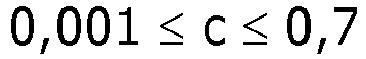


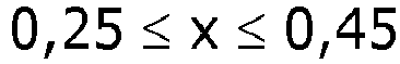

- Leuchtstoff gemäß Anspruch 1, wobei das Li-Element und das M-Element als feste Lösung in dem anorganischen Kristall eingebaut sind.
- Leuchtstoff gemäß Anspruch 2, wobei das Li-Element als interstitielle feste Lösung in dem anorganischen Kristall eingebaut ist.
- Leuchtstoff gemäß Anspruch 1, wobei es sich bei dem M-Element um Eu handelt.
- Leuchtstoff gemäß Anspruch 1, wobei der anorganische Kristall ein Kristall ist, der zu einem monoklinen System gehört und eine Symmetrie der Raumgruppe Pc aufweist, und wobei seine Gitterkonstanten a, b und c und die Winkel α, β und γ Werte in den folgenden Bereichen aufweisen:


- Leuchtstoff gemäß Anspruch 1, wobei die Parameter d, e, f und g Werte in einem Bereich aufweisen, in dem alle folgenden Bedingungen erfüllt sind:

- Leuchtstoff gemäß Anspruch 1, wobei die Parameter f und g der folgenden Bedingung genügen:

- Leuchtstoff gemäß Anspruch 1, wobei die Summenformel der anorganischen durch Liw(Sr, Ba, Eu)pSiqAlzNsOt unter Verwendung der Parameter w, p, q, z, s und t dargestellt wird, wobei:


- Leuchtstoff gemäß Anspruch 1, wobei bei Bestrahlung mit einer Anregungsquelle Fluoreszenz emittiert wird, die ein Maximum bei einer Wellenlänge in einem Bereich von 470 nm bis 620 nm aufweist.
- Leuchtstoff gemäß Anspruch 9, wobei die Anregungsquelle ein Vakuum-UV-, UV- oder sichtbares Licht mit einer Wellenlänge, die wenigstens 100 nm und nicht mehr als 410 nm beträgt, oder einen Elektronenstrahl oder Röntgenstrahl umfasst.
- Leuchtstoff gemäß Anspruch 1, wobei Li und Al und Eu als feste Lösung in einem Ba1Si7N10-Kristall eingebaut sind und wobei bei Bestrahlung mit Licht von 280 nm bis 410 nm farbiges Licht emittiert wird.
- Verfahren zur Herstellung eines Leuchtstoffs gemäß Anspruch 1, umfassend:
Brennen eines Rohstoffgemischs, das aus einem Leuchtstoff gemäß Anspruch 1 bestehen soll, in einer inerten Atmosphäre, die Stickstoff umfasst, in einem Temperaturbereich von wenigstens 1200 °C und nicht mehr als 2200 °C, wobei das Rohstoffgemisch ein Gemisch von Metallverbindungen ist und beim Brennen zu dem Leuchtstoff gemäß Anspruch 1 wird. - Lichtemittierende Vorrichtung, die wenigstens einen anregungslichtemittierenden Körper und einen Leuchtstoff umfasst, wobei der Leuchtstoff wenigstens einen Leuchtstoff gemäß Anspruch 1 umfasst.
- Bildanzeigevorrichtung, die eine Anregungsquelle und einen Leuchtstoff umfasst, wobei wenigstens ein Leuchtstoff gemäß Anspruch 1 verwendet wird.
- Pigment oder Ultraviolett-Absorber, das oder der eine anorganische Verbindung gemäß Anspruch 1 umfasst.
Applications Claiming Priority (2)
| Application Number | Priority Date | Filing Date | Title |
|---|---|---|---|
| JP2013092694 | 2013-04-25 | ||
| PCT/JP2014/061578 WO2014175385A1 (ja) | 2013-04-25 | 2014-04-24 | 蛍光体、その製造方法、発光装置および画像表示装置 |
Publications (3)
| Publication Number | Publication Date |
|---|---|
| EP2990457A1 EP2990457A1 (de) | 2016-03-02 |
| EP2990457A4 EP2990457A4 (de) | 2016-04-06 |
| EP2990457B1 true EP2990457B1 (de) | 2018-12-05 |
Family
ID=51791951
Family Applications (1)
| Application Number | Title | Priority Date | Filing Date |
|---|---|---|---|
| EP14788676.6A Active EP2990457B1 (de) | 2013-04-25 | 2014-04-24 | Leuchtstoff, verfahren zur herstellung von phosphor, lichtemittierendes bauelement und bildanzeigevorrichtung |
Country Status (4)
| Country | Link |
|---|---|
| US (1) | US9617471B2 (de) |
| EP (1) | EP2990457B1 (de) |
| JP (1) | JP6040500B2 (de) |
| WO (1) | WO2014175385A1 (de) |
Families Citing this family (10)
| Publication number | Priority date | Publication date | Assignee | Title |
|---|---|---|---|---|
| KR102214065B1 (ko) * | 2014-02-20 | 2021-02-09 | 엘지전자 주식회사 | 산 질화물 형광체, 그 제조 방법 및 이를 이용한 발광 소자 패키지 |
| KR102357584B1 (ko) * | 2014-12-17 | 2022-02-04 | 삼성전자주식회사 | 질화물 형광체, 백색 발광장치, 디스플레이 장치 및 조명장치 |
| EP3296377B1 (de) * | 2015-05-15 | 2020-06-10 | National Institute for Materials Science | Leuchtstoff, herstellungsverfahren dafür, beleuchtungsinstrument und bildanzeigevorrichtung |
| JP6739832B2 (ja) * | 2015-05-15 | 2020-08-12 | 国立研究開発法人物質・材料研究機構 | 蛍光体、その製造方法、照明器具および画像表示装置 |
| JP6020756B1 (ja) * | 2015-05-29 | 2016-11-02 | 日亜化学工業株式会社 | βサイアロン蛍光体の製造方法 |
| JP6460056B2 (ja) * | 2016-06-30 | 2019-01-30 | 日亜化学工業株式会社 | 窒化物蛍光体の製造方法 |
| JP6959601B2 (ja) * | 2016-10-27 | 2021-11-02 | 国立研究開発法人物質・材料研究機構 | 蛍光体の製造方法 |
| CN111269713A (zh) * | 2018-12-04 | 2020-06-12 | 隆达电子股份有限公司 | 氮化物荧光粉及包含氮化物荧光粉的发光元件与背光模块 |
| KR20230034287A (ko) * | 2020-07-03 | 2023-03-09 | 덴카 주식회사 | 형광체, 파장 변환체 및 발광 장치 |
| WO2022244523A1 (ja) * | 2021-05-21 | 2022-11-24 | 国立研究開発法人物質・材料研究機構 | 蛍光体、その製造方法、発光素子および発光装置 |
Family Cites Families (47)
| Publication number | Priority date | Publication date | Assignee | Title |
|---|---|---|---|---|
| US3420781A (en) * | 1966-03-14 | 1969-01-07 | Westinghouse Electric Corp | Rare earth activated strontium lithium germanate phosphors |
| US3420791A (en) | 1966-11-21 | 1969-01-07 | Dow Chemical Co | Process for making granular polymers |
| JPS528993A (en) * | 1975-07-11 | 1977-01-24 | Hitachi Ltd | Fluorescent substance |
| JPH05152609A (ja) | 1991-11-25 | 1993-06-18 | Nichia Chem Ind Ltd | 発光ダイオード |
| JPH0799345A (ja) | 1993-09-28 | 1995-04-11 | Nichia Chem Ind Ltd | 発光ダイオード |
| JP2927279B2 (ja) | 1996-07-29 | 1999-07-28 | 日亜化学工業株式会社 | 発光ダイオード |
| EP1104799A1 (de) | 1999-11-30 | 2001-06-06 | Patent-Treuhand-Gesellschaft für elektrische Glühlampen mbH | Rotstrahlendes lumineszentes Material |
| DE10105800B4 (de) | 2001-02-07 | 2017-08-31 | Osram Gmbh | Hocheffizienter Leuchtstoff und dessen Verwendung |
| JP3668770B2 (ja) | 2001-06-07 | 2005-07-06 | 独立行政法人物質・材料研究機構 | 希土類元素を付活させた酸窒化物蛍光体 |
| EP1367655A4 (de) * | 2001-09-03 | 2009-05-06 | Panasonic Corp | "halbleiter-lichtemissionsbauelement, lichtemissionsvorrichtung und herstellungsverfahren für ein halbleiter-lichtemissionsbauelement" |
| CA2447288C (en) | 2002-03-22 | 2011-10-04 | Nichia Corporation | Nitride phosphor and method for preparation thereof, and light emitting device |
| JP4214768B2 (ja) * | 2002-11-29 | 2009-01-28 | 日亜化学工業株式会社 | 窒化物蛍光体及びそれを用いた発光装置 |
| JP4218328B2 (ja) * | 2002-11-29 | 2009-02-04 | 日亜化学工業株式会社 | 窒化物蛍光体及びそれを用いた発光装置 |
| JP3837551B2 (ja) | 2003-06-20 | 2006-10-25 | 独立行政法人物質・材料研究機構 | 酸窒化物蛍光体 |
| DE112004001533B4 (de) | 2003-08-22 | 2021-07-22 | National Institute For Materials Science | Leuchtbauelement und Bildanzeige enthaltend ein fluoreszierendes Oxynitridmaterial |
| JP4806889B2 (ja) * | 2003-09-05 | 2011-11-02 | 日亜化学工業株式会社 | 光源装置及び照明装置 |
| EP1515368B1 (de) | 2003-09-05 | 2019-12-25 | Nichia Corporation | Lichtausstattung |
| JP4834827B2 (ja) | 2003-10-03 | 2011-12-14 | 独立行政法人物質・材料研究機構 | 酸窒化物蛍光体 |
| JP3837588B2 (ja) | 2003-11-26 | 2006-10-25 | 独立行政法人物質・材料研究機構 | 蛍光体と蛍光体を用いた発光器具 |
| JP2005239936A (ja) | 2004-02-27 | 2005-09-08 | Sumitomo Chemical Co Ltd | 蛍光体 |
| JP3921545B2 (ja) | 2004-03-12 | 2007-05-30 | 独立行政法人物質・材料研究機構 | 蛍光体とその製造方法 |
| JP4524368B2 (ja) | 2004-04-22 | 2010-08-18 | 独立行政法人物質・材料研究機構 | サイアロン蛍光体とその製造方法 |
| TW200644283A (en) * | 2005-02-23 | 2006-12-16 | Sumitomo Chemical Co | Fluorescent substance and light-emitting apparatus and white light emitting diode |
| US20100155753A1 (en) | 2005-02-23 | 2010-06-24 | Sumitomo Chemical Company, Limited | Phosphor, light emitting device and white light emitting diode |
| JP5013374B2 (ja) | 2005-03-22 | 2012-08-29 | 独立行政法人物質・材料研究機構 | 蛍光体とその製造方法および発光器具 |
| JP4822203B2 (ja) | 2005-04-28 | 2011-11-24 | 独立行政法人物質・材料研究機構 | リチウム含有サイアロン蛍光体およびその製造法 |
| JP5046223B2 (ja) * | 2005-05-24 | 2012-10-10 | 独立行政法人物質・材料研究機構 | 蛍光体及びその利用 |
| WO2006126567A1 (ja) | 2005-05-24 | 2006-11-30 | Mitsubishi Chemical Corporation | 蛍光体及びその利用 |
| US8147715B2 (en) | 2005-12-08 | 2012-04-03 | National Institute For Materials Science | Phosphor, process for producing the same, and luminescent device |
| KR101439567B1 (ko) * | 2006-08-15 | 2014-09-11 | 다리엔 루밍라이트 컴퍼니 리미티드 | 다방출 피크를 가지는 실리케이트계 발광물질들, 그를 제조하는 방법 및 그를 사용하는 광방출 장치들 |
| DE102007018099A1 (de) | 2007-04-17 | 2008-10-23 | Osram Gesellschaft mit beschränkter Haftung | Rot emittierender Leuchtstoff und Lichtquelle mit derartigem Leuchtstoff |
| JP4474491B1 (ja) | 2009-08-11 | 2010-06-02 | キヤノン・コンポーネンツ株式会社 | 白色発光装置およびそれを用いたライン状照明装置 |
| EP2163593A1 (de) * | 2008-09-15 | 2010-03-17 | Max-Planck-Gesellschaft zur Förderung der Wissenschaften e.V. | Herstellung von nitridbasiertem Phosphor |
| CN102348778B (zh) * | 2009-03-26 | 2014-09-10 | 独立行政法人物质·材料研究机构 | 荧光体、其制造方法、发光器具以及图像显示装置 |
| WO2010119375A1 (en) * | 2009-04-16 | 2010-10-21 | Koninklijke Philips Electronics N.V. | Red emitting luminescent materials |
| JP2011052099A (ja) | 2009-09-01 | 2011-03-17 | Mitsubishi Chemicals Corp | 窒化物蛍光体の製造方法 |
| CN101760194B (zh) * | 2009-12-30 | 2014-03-19 | 李�瑞 | 一种白光led用红色荧光粉及其制备方法 |
| CN101760191B (zh) | 2010-01-20 | 2013-01-09 | 浙江大学 | Led用高亮度硅酸钡基蓝绿色荧光粉及其高温还原制备方法 |
| CN102559177B (zh) * | 2010-12-28 | 2014-09-03 | 北京宇极科技发展有限公司 | 一种氮氧化合物发光材料、其制备方法以及由其制成的照明光源 |
| US20130127333A1 (en) | 2010-12-28 | 2013-05-23 | Beijing Yuji Science And Technology Co. Ltd | Oxynitride luminescent material, preparation method thereof and illumination light source made from such material |
| JP5697473B2 (ja) | 2011-02-06 | 2015-04-08 | 独立行政法人物質・材料研究機構 | 蛍光体、その製造方法及び発光装置 |
| JP5795971B2 (ja) | 2012-03-07 | 2015-10-14 | パナソニック株式会社 | 蛍光体及び発光装置 |
| WO2013180216A1 (ja) * | 2012-05-31 | 2013-12-05 | 独立行政法人物質・材料研究機構 | 蛍光体、その製造方法、発光装置および画像表示装置 |
| KR101662924B1 (ko) | 2012-06-27 | 2016-10-05 | 코쿠리츠켄큐카이하츠호징 붓시쯔 자이료 켄큐키코 | 형광체, 그 제조 방법, 발광 장치 및 화상 표시 장치 |
| JP6057213B2 (ja) | 2012-07-10 | 2017-01-11 | 国立研究開発法人物質・材料研究機構 | 蛍光体、その製造方法、発光装置および画像表示装置 |
| JP6036055B2 (ja) * | 2012-09-12 | 2016-11-30 | 日亜化学工業株式会社 | 蛍光体及びこれを用いた発光装置 |
| CN102925153B (zh) | 2012-11-23 | 2014-01-15 | 中国科学院长春光学精密机械与物理研究所 | 颜色可调的单一相荧光材料及其应用 |
-
2014
- 2014-04-24 EP EP14788676.6A patent/EP2990457B1/de active Active
- 2014-04-24 JP JP2015513832A patent/JP6040500B2/ja active Active
- 2014-04-24 WO PCT/JP2014/061578 patent/WO2014175385A1/ja active Application Filing
- 2014-04-24 US US14/786,248 patent/US9617471B2/en active Active
Non-Patent Citations (1)
| Title |
|---|
| None * |
Also Published As
| Publication number | Publication date |
|---|---|
| JPWO2014175385A1 (ja) | 2017-02-23 |
| JP6040500B2 (ja) | 2016-12-07 |
| US20160060518A1 (en) | 2016-03-03 |
| US9617471B2 (en) | 2017-04-11 |
| EP2990457A4 (de) | 2016-04-06 |
| EP2990457A1 (de) | 2016-03-02 |
| WO2014175385A1 (ja) | 2014-10-30 |
Similar Documents
| Publication | Publication Date | Title |
|---|---|---|
| EP2998381B1 (de) | Leuchtstoff, herstellungsverfahren dafür, lichtemittierende vorrichtung, bildanzeigevorrichtung, pigment und uv-absorber | |
| EP2787056B1 (de) | Leuchtstoff, herstellungsverfahren dafür, lichtemittierende vorrichtung und bildanzeigevorrichtung | |
| EP2801599B1 (de) | Leuchtstoff, herstellungsverfahren dafür, lichtemittierende vorrichtung, und bildanzeigevorrichtung | |
| EP2868730B1 (de) | Phosphor, verfahren zur herstellung von phosphor, lichtemittierendes bauelement und bildanzeigevorrichtung | |
| EP2990457B1 (de) | Leuchtstoff, verfahren zur herstellung von phosphor, lichtemittierendes bauelement und bildanzeigevorrichtung | |
| EP2878647B1 (de) | Fluorophor, verfahren zu seiner herstellung, lichtemittierendes bauelement und bildanzeigevorrichtung | |
| JP6057213B2 (ja) | 蛍光体、その製造方法、発光装置および画像表示装置 | |
| EP3992264B1 (de) | Fluoreszenzkörper, verfahren zu seiner herstellung und lichtemittierende vorrichtung damit | |
| JP2017210529A (ja) | 蛍光体、その製造方法、発光装置、画像表示装置、顔料、および、紫外線吸収剤 | |
| EP4339260A1 (de) | Phosphor, verfahren zur herstellung desselben, lichtemittierendes element und lichtemittierende vorrichtung |
Legal Events
| Date | Code | Title | Description |
|---|---|---|---|
| PUAI | Public reference made under article 153(3) epc to a published international application that has entered the european phase |
Free format text: ORIGINAL CODE: 0009012 |
|
| 17P | Request for examination filed |
Effective date: 20151117 |
|
| AK | Designated contracting states |
Kind code of ref document: A1 Designated state(s): AL AT BE BG CH CY CZ DE DK EE ES FI FR GB GR HR HU IE IS IT LI LT LU LV MC MK MT NL NO PL PT RO RS SE SI SK SM TR |
|
| AX | Request for extension of the european patent |
Extension state: BA ME |
|
| A4 | Supplementary search report drawn up and despatched |
Effective date: 20160308 |
|
| RIC1 | Information provided on ipc code assigned before grant |
Ipc: H01L 51/50 20060101ALI20160302BHEP Ipc: C09K 11/59 20060101ALI20160302BHEP Ipc: H05B 33/12 20060101ALI20160302BHEP Ipc: C09K 11/55 20060101AFI20160302BHEP Ipc: C09K 11/64 20060101ALI20160302BHEP Ipc: H01L 33/50 20100101ALI20160302BHEP Ipc: C09K 3/00 20060101ALI20160302BHEP Ipc: C09K 11/08 20060101ALI20160302BHEP |
|
| DAX | Request for extension of the european patent (deleted) | ||
| STAA | Information on the status of an ep patent application or granted ep patent |
Free format text: STATUS: EXAMINATION IS IN PROGRESS |
|
| 17Q | First examination report despatched |
Effective date: 20170801 |
|
| REG | Reference to a national code |
Ref country code: DE Ref legal event code: R079 Ref document number: 602014037488 Country of ref document: DE Free format text: PREVIOUS MAIN CLASS: C09K0011550000 Ipc: C09K0011590000 |
|
| GRAP | Despatch of communication of intention to grant a patent |
Free format text: ORIGINAL CODE: EPIDOSNIGR1 |
|
| STAA | Information on the status of an ep patent application or granted ep patent |
Free format text: STATUS: GRANT OF PATENT IS INTENDED |
|
| RIC1 | Information provided on ipc code assigned before grant |
Ipc: C09K 11/64 20060101ALI20180529BHEP Ipc: H01L 33/50 20100101ALI20180529BHEP Ipc: C09K 11/59 20060101AFI20180529BHEP |
|
| INTG | Intention to grant announced |
Effective date: 20180627 |
|
| GRAS | Grant fee paid |
Free format text: ORIGINAL CODE: EPIDOSNIGR3 |
|
| GRAA | (expected) grant |
Free format text: ORIGINAL CODE: 0009210 |
|
| STAA | Information on the status of an ep patent application or granted ep patent |
Free format text: STATUS: THE PATENT HAS BEEN GRANTED |
|
| AK | Designated contracting states |
Kind code of ref document: B1 Designated state(s): AL AT BE BG CH CY CZ DE DK EE ES FI FR GB GR HR HU IE IS IT LI LT LU LV MC MK MT NL NO PL PT RO RS SE SI SK SM TR |
|
| REG | Reference to a national code |
Ref country code: GB Ref legal event code: FG4D |
|
| REG | Reference to a national code |
Ref country code: CH Ref legal event code: EP |
|
| REG | Reference to a national code |
Ref country code: AT Ref legal event code: REF Ref document number: 1073031 Country of ref document: AT Kind code of ref document: T Effective date: 20181215 |
|
| REG | Reference to a national code |
Ref country code: IE Ref legal event code: FG4D |
|
| REG | Reference to a national code |
Ref country code: DE Ref legal event code: R096 Ref document number: 602014037488 Country of ref document: DE |
|
| REG | Reference to a national code |
Ref country code: NL Ref legal event code: MP Effective date: 20181205 |
|
| REG | Reference to a national code |
Ref country code: AT Ref legal event code: MK05 Ref document number: 1073031 Country of ref document: AT Kind code of ref document: T Effective date: 20181205 |
|
| REG | Reference to a national code |
Ref country code: LT Ref legal event code: MG4D |
|
| PG25 | Lapsed in a contracting state [announced via postgrant information from national office to epo] |
Ref country code: LV Free format text: LAPSE BECAUSE OF FAILURE TO SUBMIT A TRANSLATION OF THE DESCRIPTION OR TO PAY THE FEE WITHIN THE PRESCRIBED TIME-LIMIT Effective date: 20181205 Ref country code: ES Free format text: LAPSE BECAUSE OF FAILURE TO SUBMIT A TRANSLATION OF THE DESCRIPTION OR TO PAY THE FEE WITHIN THE PRESCRIBED TIME-LIMIT Effective date: 20181205 Ref country code: AT Free format text: LAPSE BECAUSE OF FAILURE TO SUBMIT A TRANSLATION OF THE DESCRIPTION OR TO PAY THE FEE WITHIN THE PRESCRIBED TIME-LIMIT Effective date: 20181205 Ref country code: HR Free format text: LAPSE BECAUSE OF FAILURE TO SUBMIT A TRANSLATION OF THE DESCRIPTION OR TO PAY THE FEE WITHIN THE PRESCRIBED TIME-LIMIT Effective date: 20181205 Ref country code: NO Free format text: LAPSE BECAUSE OF FAILURE TO SUBMIT A TRANSLATION OF THE DESCRIPTION OR TO PAY THE FEE WITHIN THE PRESCRIBED TIME-LIMIT Effective date: 20190305 Ref country code: LT Free format text: LAPSE BECAUSE OF FAILURE TO SUBMIT A TRANSLATION OF THE DESCRIPTION OR TO PAY THE FEE WITHIN THE PRESCRIBED TIME-LIMIT Effective date: 20181205 Ref country code: BG Free format text: LAPSE BECAUSE OF FAILURE TO SUBMIT A TRANSLATION OF THE DESCRIPTION OR TO PAY THE FEE WITHIN THE PRESCRIBED TIME-LIMIT Effective date: 20190305 Ref country code: FI Free format text: LAPSE BECAUSE OF FAILURE TO SUBMIT A TRANSLATION OF THE DESCRIPTION OR TO PAY THE FEE WITHIN THE PRESCRIBED TIME-LIMIT Effective date: 20181205 |
|
| PG25 | Lapsed in a contracting state [announced via postgrant information from national office to epo] |
Ref country code: GR Free format text: LAPSE BECAUSE OF FAILURE TO SUBMIT A TRANSLATION OF THE DESCRIPTION OR TO PAY THE FEE WITHIN THE PRESCRIBED TIME-LIMIT Effective date: 20190306 Ref country code: RS Free format text: LAPSE BECAUSE OF FAILURE TO SUBMIT A TRANSLATION OF THE DESCRIPTION OR TO PAY THE FEE WITHIN THE PRESCRIBED TIME-LIMIT Effective date: 20181205 Ref country code: SE Free format text: LAPSE BECAUSE OF FAILURE TO SUBMIT A TRANSLATION OF THE DESCRIPTION OR TO PAY THE FEE WITHIN THE PRESCRIBED TIME-LIMIT Effective date: 20181205 Ref country code: AL Free format text: LAPSE BECAUSE OF FAILURE TO SUBMIT A TRANSLATION OF THE DESCRIPTION OR TO PAY THE FEE WITHIN THE PRESCRIBED TIME-LIMIT Effective date: 20181205 |
|
| PG25 | Lapsed in a contracting state [announced via postgrant information from national office to epo] |
Ref country code: NL Free format text: LAPSE BECAUSE OF FAILURE TO SUBMIT A TRANSLATION OF THE DESCRIPTION OR TO PAY THE FEE WITHIN THE PRESCRIBED TIME-LIMIT Effective date: 20181205 |
|
| PG25 | Lapsed in a contracting state [announced via postgrant information from national office to epo] |
Ref country code: PL Free format text: LAPSE BECAUSE OF FAILURE TO SUBMIT A TRANSLATION OF THE DESCRIPTION OR TO PAY THE FEE WITHIN THE PRESCRIBED TIME-LIMIT Effective date: 20181205 Ref country code: IT Free format text: LAPSE BECAUSE OF FAILURE TO SUBMIT A TRANSLATION OF THE DESCRIPTION OR TO PAY THE FEE WITHIN THE PRESCRIBED TIME-LIMIT Effective date: 20181205 Ref country code: CZ Free format text: LAPSE BECAUSE OF FAILURE TO SUBMIT A TRANSLATION OF THE DESCRIPTION OR TO PAY THE FEE WITHIN THE PRESCRIBED TIME-LIMIT Effective date: 20181205 Ref country code: PT Free format text: LAPSE BECAUSE OF FAILURE TO SUBMIT A TRANSLATION OF THE DESCRIPTION OR TO PAY THE FEE WITHIN THE PRESCRIBED TIME-LIMIT Effective date: 20190405 |
|
| PG25 | Lapsed in a contracting state [announced via postgrant information from national office to epo] |
Ref country code: IS Free format text: LAPSE BECAUSE OF FAILURE TO SUBMIT A TRANSLATION OF THE DESCRIPTION OR TO PAY THE FEE WITHIN THE PRESCRIBED TIME-LIMIT Effective date: 20190405 Ref country code: RO Free format text: LAPSE BECAUSE OF FAILURE TO SUBMIT A TRANSLATION OF THE DESCRIPTION OR TO PAY THE FEE WITHIN THE PRESCRIBED TIME-LIMIT Effective date: 20181205 Ref country code: SM Free format text: LAPSE BECAUSE OF FAILURE TO SUBMIT A TRANSLATION OF THE DESCRIPTION OR TO PAY THE FEE WITHIN THE PRESCRIBED TIME-LIMIT Effective date: 20181205 Ref country code: EE Free format text: LAPSE BECAUSE OF FAILURE TO SUBMIT A TRANSLATION OF THE DESCRIPTION OR TO PAY THE FEE WITHIN THE PRESCRIBED TIME-LIMIT Effective date: 20181205 Ref country code: SK Free format text: LAPSE BECAUSE OF FAILURE TO SUBMIT A TRANSLATION OF THE DESCRIPTION OR TO PAY THE FEE WITHIN THE PRESCRIBED TIME-LIMIT Effective date: 20181205 |
|
| REG | Reference to a national code |
Ref country code: DE Ref legal event code: R097 Ref document number: 602014037488 Country of ref document: DE |
|
| PLBE | No opposition filed within time limit |
Free format text: ORIGINAL CODE: 0009261 |
|
| STAA | Information on the status of an ep patent application or granted ep patent |
Free format text: STATUS: NO OPPOSITION FILED WITHIN TIME LIMIT |
|
| PG25 | Lapsed in a contracting state [announced via postgrant information from national office to epo] |
Ref country code: SI Free format text: LAPSE BECAUSE OF FAILURE TO SUBMIT A TRANSLATION OF THE DESCRIPTION OR TO PAY THE FEE WITHIN THE PRESCRIBED TIME-LIMIT Effective date: 20181205 Ref country code: DK Free format text: LAPSE BECAUSE OF FAILURE TO SUBMIT A TRANSLATION OF THE DESCRIPTION OR TO PAY THE FEE WITHIN THE PRESCRIBED TIME-LIMIT Effective date: 20181205 |
|
| 26N | No opposition filed |
Effective date: 20190906 |
|
| REG | Reference to a national code |
Ref country code: CH Ref legal event code: PL |
|
| REG | Reference to a national code |
Ref country code: BE Ref legal event code: MM Effective date: 20190430 |
|
| GBPC | Gb: european patent ceased through non-payment of renewal fee |
Effective date: 20190424 |
|
| PG25 | Lapsed in a contracting state [announced via postgrant information from national office to epo] |
Ref country code: LU Free format text: LAPSE BECAUSE OF NON-PAYMENT OF DUE FEES Effective date: 20190424 Ref country code: MC Free format text: LAPSE BECAUSE OF FAILURE TO SUBMIT A TRANSLATION OF THE DESCRIPTION OR TO PAY THE FEE WITHIN THE PRESCRIBED TIME-LIMIT Effective date: 20181205 |
|
| PG25 | Lapsed in a contracting state [announced via postgrant information from national office to epo] |
Ref country code: CH Free format text: LAPSE BECAUSE OF NON-PAYMENT OF DUE FEES Effective date: 20190430 Ref country code: LI Free format text: LAPSE BECAUSE OF NON-PAYMENT OF DUE FEES Effective date: 20190430 Ref country code: GB Free format text: LAPSE BECAUSE OF NON-PAYMENT OF DUE FEES Effective date: 20190424 |
|
| PG25 | Lapsed in a contracting state [announced via postgrant information from national office to epo] |
Ref country code: BE Free format text: LAPSE BECAUSE OF NON-PAYMENT OF DUE FEES Effective date: 20190430 |
|
| PG25 | Lapsed in a contracting state [announced via postgrant information from national office to epo] |
Ref country code: TR Free format text: LAPSE BECAUSE OF FAILURE TO SUBMIT A TRANSLATION OF THE DESCRIPTION OR TO PAY THE FEE WITHIN THE PRESCRIBED TIME-LIMIT Effective date: 20181205 |
|
| PG25 | Lapsed in a contracting state [announced via postgrant information from national office to epo] |
Ref country code: IE Free format text: LAPSE BECAUSE OF NON-PAYMENT OF DUE FEES Effective date: 20190424 |
|
| PG25 | Lapsed in a contracting state [announced via postgrant information from national office to epo] |
Ref country code: CY Free format text: LAPSE BECAUSE OF FAILURE TO SUBMIT A TRANSLATION OF THE DESCRIPTION OR TO PAY THE FEE WITHIN THE PRESCRIBED TIME-LIMIT Effective date: 20181205 |
|
| PG25 | Lapsed in a contracting state [announced via postgrant information from national office to epo] |
Ref country code: HU Free format text: LAPSE BECAUSE OF FAILURE TO SUBMIT A TRANSLATION OF THE DESCRIPTION OR TO PAY THE FEE WITHIN THE PRESCRIBED TIME-LIMIT; INVALID AB INITIO Effective date: 20140424 Ref country code: MT Free format text: LAPSE BECAUSE OF FAILURE TO SUBMIT A TRANSLATION OF THE DESCRIPTION OR TO PAY THE FEE WITHIN THE PRESCRIBED TIME-LIMIT Effective date: 20181205 |
|
| PG25 | Lapsed in a contracting state [announced via postgrant information from national office to epo] |
Ref country code: MK Free format text: LAPSE BECAUSE OF FAILURE TO SUBMIT A TRANSLATION OF THE DESCRIPTION OR TO PAY THE FEE WITHIN THE PRESCRIBED TIME-LIMIT Effective date: 20181205 |
|
| P01 | Opt-out of the competence of the unified patent court (upc) registered |
Effective date: 20230526 |
|
| PGFP | Annual fee paid to national office [announced via postgrant information from national office to epo] |
Ref country code: FR Payment date: 20230417 Year of fee payment: 10 Ref country code: DE Payment date: 20230426 Year of fee payment: 10 |