EP2959520B1 - Composant optoélectronique - Google Patents
Composant optoélectronique Download PDFInfo
- Publication number
- EP2959520B1 EP2959520B1 EP14709574.9A EP14709574A EP2959520B1 EP 2959520 B1 EP2959520 B1 EP 2959520B1 EP 14709574 A EP14709574 A EP 14709574A EP 2959520 B1 EP2959520 B1 EP 2959520B1
- Authority
- EP
- European Patent Office
- Prior art keywords
- donor
- acceptor
- optoelectronic component
- component according
- photoactive layer
- Prior art date
- Legal status (The legal status is an assumption and is not a legal conclusion. Google has not performed a legal analysis and makes no representation as to the accuracy of the status listed.)
- Active
Links
- 230000005693 optoelectronics Effects 0.000 title claims description 30
- 239000000463 material Substances 0.000 claims description 203
- 150000001875 compounds Chemical class 0.000 claims description 29
- 238000004768 lowest unoccupied molecular orbital Methods 0.000 claims description 28
- 238000004770 highest occupied molecular orbital Methods 0.000 claims description 27
- 125000001997 phenyl group Chemical group [H]C1=C([H])C([H])=C(*)C([H])=C1[H] 0.000 claims description 26
- SIKJAQJRHWYJAI-UHFFFAOYSA-N Indole Chemical compound C1=CC=C2NC=CC2=C1 SIKJAQJRHWYJAI-UHFFFAOYSA-N 0.000 claims description 20
- FCEHBMOGCRZNNI-UHFFFAOYSA-N 1-benzothiophene Chemical class C1=CC=C2SC=CC2=C1 FCEHBMOGCRZNNI-UHFFFAOYSA-N 0.000 claims description 18
- YTPLMLYBLZKORZ-UHFFFAOYSA-N Thiophene Chemical group C=1C=CSC=1 YTPLMLYBLZKORZ-UHFFFAOYSA-N 0.000 claims description 15
- 150000003983 crown ethers Chemical class 0.000 claims description 15
- 238000002425 crystallisation Methods 0.000 claims description 13
- 230000008025 crystallization Effects 0.000 claims description 13
- YLQBMQCUIZJEEH-UHFFFAOYSA-N Furan Chemical compound C=1C=COC=1 YLQBMQCUIZJEEH-UHFFFAOYSA-N 0.000 claims description 12
- KAESVJOAVNADME-UHFFFAOYSA-N Pyrrole Chemical compound C=1C=CNC=1 KAESVJOAVNADME-UHFFFAOYSA-N 0.000 claims description 12
- RFRXIWQYSOIBDI-UHFFFAOYSA-N benzarone Chemical compound CCC=1OC2=CC=CC=C2C=1C(=O)C1=CC=C(O)C=C1 RFRXIWQYSOIBDI-UHFFFAOYSA-N 0.000 claims description 12
- 230000007547 defect Effects 0.000 claims description 12
- ZUOUZKKEUPVFJK-UHFFFAOYSA-N diphenyl Chemical compound C1=CC=CC=C1C1=CC=CC=C1 ZUOUZKKEUPVFJK-UHFFFAOYSA-N 0.000 claims description 12
- 125000001072 heteroaryl group Chemical group 0.000 claims description 12
- 125000001624 naphthyl group Chemical group 0.000 claims description 12
- KYQCOXFCLRTKLS-UHFFFAOYSA-N Pyrazine Chemical compound C1=CN=CC=N1 KYQCOXFCLRTKLS-UHFFFAOYSA-N 0.000 claims description 10
- JUJWROOIHBZHMG-UHFFFAOYSA-N Pyridine Chemical compound C1=CC=NC=C1 JUJWROOIHBZHMG-UHFFFAOYSA-N 0.000 claims description 10
- IOJUPLGTWVMSFF-UHFFFAOYSA-N benzothiazole Chemical compound C1=CC=C2SC=NC2=C1 IOJUPLGTWVMSFF-UHFFFAOYSA-N 0.000 claims description 10
- 150000003384 small molecules Chemical class 0.000 claims description 9
- YJTKZCDBKVTVBY-UHFFFAOYSA-N 1,3-Diphenylbenzene Chemical group C1=CC=CC=C1C1=CC=CC(C=2C=CC=CC=2)=C1 YJTKZCDBKVTVBY-UHFFFAOYSA-N 0.000 claims description 6
- BCMCBBGGLRIHSE-UHFFFAOYSA-N 1,3-benzoxazole Chemical compound C1=CC=C2OC=NC2=C1 BCMCBBGGLRIHSE-UHFFFAOYSA-N 0.000 claims description 6
- ZCQWOFVYLHDMMC-UHFFFAOYSA-N Oxazole Chemical compound C1=COC=N1 ZCQWOFVYLHDMMC-UHFFFAOYSA-N 0.000 claims description 6
- CZPWVGJYEJSRLH-UHFFFAOYSA-N Pyrimidine Chemical compound C1=CN=CN=C1 CZPWVGJYEJSRLH-UHFFFAOYSA-N 0.000 claims description 6
- FZWLAAWBMGSTSO-UHFFFAOYSA-N Thiazole Chemical compound C1=CSC=N1 FZWLAAWBMGSTSO-UHFFFAOYSA-N 0.000 claims description 6
- 125000002178 anthracenyl group Chemical group C1(=CC=CC2=CC3=CC=CC=C3C=C12)* 0.000 claims description 6
- ZDZHCHYQNPQSGG-UHFFFAOYSA-N binaphthyl group Chemical group C1(=CC=CC2=CC=CC=C12)C1=CC=CC2=CC=CC=C12 ZDZHCHYQNPQSGG-UHFFFAOYSA-N 0.000 claims description 6
- 235000010290 biphenyl Nutrition 0.000 claims description 6
- 239000004305 biphenyl Substances 0.000 claims description 6
- WCPAKWJPBJAGKN-UHFFFAOYSA-N oxadiazole Chemical compound C1=CON=N1 WCPAKWJPBJAGKN-UHFFFAOYSA-N 0.000 claims description 6
- 125000001792 phenanthrenyl group Chemical group C1(=CC=CC=2C3=CC=CC=C3C=CC12)* 0.000 claims description 6
- 125000001725 pyrenyl group Chemical group 0.000 claims description 6
- ONCNIMLKGZSAJT-UHFFFAOYSA-N thieno[3,2-b]furan Chemical compound S1C=CC2=C1C=CO2 ONCNIMLKGZSAJT-UHFFFAOYSA-N 0.000 claims description 6
- 229930192474 thiophene Natural products 0.000 claims description 6
- 125000000959 isobutyl group Chemical group [H]C([H])([H])C([H])(C([H])([H])[H])C([H])([H])* 0.000 claims description 5
- 239000011368 organic material Substances 0.000 claims description 5
- BKYWEUVIGUEMFX-UHFFFAOYSA-N 4h-dithieno[3,2-a:2',3'-d]pyrrole Chemical compound S1C=CC2=C1NC1=C2SC=C1 BKYWEUVIGUEMFX-UHFFFAOYSA-N 0.000 claims description 4
- PCNDJXKNXGMECE-UHFFFAOYSA-N Phenazine Natural products C1=CC=CC2=NC3=CC=CC=C3N=C21 PCNDJXKNXGMECE-UHFFFAOYSA-N 0.000 claims description 4
- HKNRNTYTYUWGLN-UHFFFAOYSA-N dithieno[3,2-a:2',3'-d]thiophene Chemical compound C1=CSC2=C1SC1=C2C=CS1 HKNRNTYTYUWGLN-UHFFFAOYSA-N 0.000 claims description 4
- RTZKZFJDLAIYFH-UHFFFAOYSA-N ether Substances CCOCC RTZKZFJDLAIYFH-UHFFFAOYSA-N 0.000 claims description 4
- 125000000623 heterocyclic group Chemical group 0.000 claims description 4
- 238000005191 phase separation Methods 0.000 claims description 4
- UMJSCPRVCHMLSP-UHFFFAOYSA-N pyridine Natural products COC1=CC=CN=C1 UMJSCPRVCHMLSP-UHFFFAOYSA-N 0.000 claims description 4
- VLLMWSRANPNYQX-UHFFFAOYSA-N thiadiazole Chemical compound C1=CSN=N1.C1=CSN=N1 VLLMWSRANPNYQX-UHFFFAOYSA-N 0.000 claims description 4
- 150000003852 triazoles Chemical class 0.000 claims description 4
- 238000000926 separation method Methods 0.000 claims description 3
- 230000001737 promoting effect Effects 0.000 claims 1
- 239000000758 substrate Substances 0.000 description 15
- 239000002800 charge carrier Substances 0.000 description 14
- -1 Thienopyrrol Chemical compound 0.000 description 12
- 230000008021 deposition Effects 0.000 description 11
- 238000011049 filling Methods 0.000 description 10
- 238000005259 measurement Methods 0.000 description 10
- XMWRBQBLMFGWIX-UHFFFAOYSA-N C60 fullerene Chemical class C12=C3C(C4=C56)=C7C8=C5C5=C9C%10=C6C6=C4C1=C1C4=C6C6=C%10C%10=C9C9=C%11C5=C8C5=C8C7=C3C3=C7C2=C1C1=C2C4=C6C4=C%10C6=C9C9=C%11C5=C5C8=C3C3=C7C1=C1C2=C4C6=C2C9=C5C3=C12 XMWRBQBLMFGWIX-UHFFFAOYSA-N 0.000 description 8
- 125000003118 aryl group Chemical group 0.000 description 8
- 239000013078 crystal Substances 0.000 description 6
- 229910003472 fullerene Inorganic materials 0.000 description 5
- 125000003545 alkoxy group Chemical group 0.000 description 4
- 238000009792 diffusion process Methods 0.000 description 4
- 125000001301 ethoxy group Chemical group [H]C([H])([H])C([H])([H])O* 0.000 description 4
- 239000012071 phase Substances 0.000 description 4
- 229920000642 polymer Polymers 0.000 description 4
- 239000006096 absorbing agent Substances 0.000 description 3
- 238000010521 absorption reaction Methods 0.000 description 3
- 239000000654 additive Substances 0.000 description 3
- 125000004432 carbon atom Chemical group C* 0.000 description 3
- 239000004020 conductor Substances 0.000 description 3
- 230000001965 increasing effect Effects 0.000 description 3
- 238000004519 manufacturing process Methods 0.000 description 3
- 229910052751 metal Inorganic materials 0.000 description 3
- 239000002184 metal Substances 0.000 description 3
- 238000005215 recombination Methods 0.000 description 3
- 230000006798 recombination Effects 0.000 description 3
- QWENRTYMTSOGBR-UHFFFAOYSA-N 1H-1,2,3-Triazole Chemical compound C=1C=NNN=1 QWENRTYMTSOGBR-UHFFFAOYSA-N 0.000 description 2
- NXVNUSIHWZLMGF-UHFFFAOYSA-N 4-phenyl-N-(4-phenylphenyl)-N-[4-[9-[4-(4-phenyl-N-(4-phenylphenyl)anilino)phenyl]fluoren-9-yl]phenyl]aniline Chemical compound C1=CC=CC=C1C1=CC=C(N(C=2C=CC(=CC=2)C=2C=CC=CC=2)C=2C=CC(=CC=2)C2(C3=CC=CC=C3C3=CC=CC=C32)C=2C=CC(=CC=2)N(C=2C=CC(=CC=2)C=2C=CC=CC=2)C=2C=CC(=CC=2)C=2C=CC=CC=2)C=C1 NXVNUSIHWZLMGF-UHFFFAOYSA-N 0.000 description 2
- 239000011149 active material Substances 0.000 description 2
- 229910021417 amorphous silicon Inorganic materials 0.000 description 2
- YSSSPARMOAYJTE-UHFFFAOYSA-N dibenzo-18-crown-6 Chemical compound O1CCOCCOC2=CC=CC=C2OCCOCCOC2=CC=CC=C21 YSSSPARMOAYJTE-UHFFFAOYSA-N 0.000 description 2
- 230000005684 electric field Effects 0.000 description 2
- 239000010408 film Substances 0.000 description 2
- 230000005525 hole transport Effects 0.000 description 2
- 239000000203 mixture Substances 0.000 description 2
- LQNUZADURLCDLV-UHFFFAOYSA-N nitrobenzene Chemical compound [O-][N+](=O)C1=CC=CC=C1 LQNUZADURLCDLV-UHFFFAOYSA-N 0.000 description 2
- 125000002080 perylenyl group Chemical class C1(=CC=C2C=CC=C3C4=CC=CC5=CC=CC(C1=C23)=C45)* 0.000 description 2
- 125000005575 polycyclic aromatic hydrocarbon group Chemical group 0.000 description 2
- 239000007790 solid phase Substances 0.000 description 2
- VJYJJHQEVLEOFL-UHFFFAOYSA-N thieno[3,2-b]thiophene Chemical compound S1C=CC2=C1C=CS2 VJYJJHQEVLEOFL-UHFFFAOYSA-N 0.000 description 2
- 239000010409 thin film Substances 0.000 description 2
- 150000003573 thiols Chemical class 0.000 description 2
- KZDTZHQLABJVLE-UHFFFAOYSA-N 1,8-diiodooctane Chemical compound ICCCCCCCCI KZDTZHQLABJVLE-UHFFFAOYSA-N 0.000 description 1
- JTPNRXUCIXHOKM-UHFFFAOYSA-N 1-chloronaphthalene Chemical compound C1=CC=C2C(Cl)=CC=CC2=C1 JTPNRXUCIXHOKM-UHFFFAOYSA-N 0.000 description 1
- JBRZTFJDHDCESZ-UHFFFAOYSA-N AsGa Chemical compound [As]#[Ga] JBRZTFJDHDCESZ-UHFFFAOYSA-N 0.000 description 1
- 229910001218 Gallium arsenide Inorganic materials 0.000 description 1
- 229920000144 PEDOT:PSS Polymers 0.000 description 1
- XUIMIQQOPSSXEZ-UHFFFAOYSA-N Silicon Chemical compound [Si] XUIMIQQOPSSXEZ-UHFFFAOYSA-N 0.000 description 1
- MCEWYIDBDVPMES-UHFFFAOYSA-N [60]pcbm Chemical compound C123C(C4=C5C6=C7C8=C9C%10=C%11C%12=C%13C%14=C%15C%16=C%17C%18=C(C=%19C=%20C%18=C%18C%16=C%13C%13=C%11C9=C9C7=C(C=%20C9=C%13%18)C(C7=%19)=C96)C6=C%11C%17=C%15C%13=C%15C%14=C%12C%12=C%10C%10=C85)=C9C7=C6C2=C%11C%13=C2C%15=C%12C%10=C4C23C1(CCCC(=O)OC)C1=CC=CC=C1 MCEWYIDBDVPMES-UHFFFAOYSA-N 0.000 description 1
- 230000006978 adaptation Effects 0.000 description 1
- 125000002029 aromatic hydrocarbon group Chemical group 0.000 description 1
- 125000005605 benzo group Chemical group 0.000 description 1
- 125000002619 bicyclic group Chemical group 0.000 description 1
- 230000008033 biological extinction Effects 0.000 description 1
- 230000015572 biosynthetic process Effects 0.000 description 1
- KCXQZTKOKSWXHY-UHFFFAOYSA-L bis[(4-tert-butylbenzoyl)oxy]aluminum;hydrate Chemical compound O.C1=CC(C(C)(C)C)=CC=C1C(=O)O[Al]OC(=O)C1=CC=C(C(C)(C)C)C=C1 KCXQZTKOKSWXHY-UHFFFAOYSA-L 0.000 description 1
- 229910052799 carbon Inorganic materials 0.000 description 1
- 238000006243 chemical reaction Methods 0.000 description 1
- 239000007795 chemical reaction product Substances 0.000 description 1
- 230000000295 complement effect Effects 0.000 description 1
- 229920001940 conductive polymer Polymers 0.000 description 1
- 238000002484 cyclic voltammetry Methods 0.000 description 1
- 238000000354 decomposition reaction Methods 0.000 description 1
- 230000001419 dependent effect Effects 0.000 description 1
- 230000002708 enhancing effect Effects 0.000 description 1
- 230000003203 everyday effect Effects 0.000 description 1
- 230000005284 excitation Effects 0.000 description 1
- 239000003574 free electron Substances 0.000 description 1
- 229910052733 gallium Inorganic materials 0.000 description 1
- 239000011521 glass Substances 0.000 description 1
- 239000012535 impurity Substances 0.000 description 1
- 238000010348 incorporation Methods 0.000 description 1
- 229910052738 indium Inorganic materials 0.000 description 1
- 150000002739 metals Chemical class 0.000 description 1
- 238000002156 mixing Methods 0.000 description 1
- 230000037230 mobility Effects 0.000 description 1
- 230000007935 neutral effect Effects 0.000 description 1
- YCWSUKQGVSGXJO-NTUHNPAUSA-N nifuroxazide Chemical group C1=CC(O)=CC=C1C(=O)N\N=C\C1=CC=C([N+]([O-])=O)O1 YCWSUKQGVSGXJO-NTUHNPAUSA-N 0.000 description 1
- 230000003287 optical effect Effects 0.000 description 1
- 238000005325 percolation Methods 0.000 description 1
- 230000000737 periodic effect Effects 0.000 description 1
- 239000004033 plastic Substances 0.000 description 1
- 239000002985 plastic film Substances 0.000 description 1
- 229920006255 plastic film Polymers 0.000 description 1
- 229920000301 poly(3-hexylthiophene-2,5-diyl) polymer Polymers 0.000 description 1
- 229920000767 polyaniline Polymers 0.000 description 1
- 238000006862 quantum yield reaction Methods 0.000 description 1
- 230000009257 reactivity Effects 0.000 description 1
- 229910052711 selenium Inorganic materials 0.000 description 1
- 239000004065 semiconductor Substances 0.000 description 1
- 229910052710 silicon Inorganic materials 0.000 description 1
- 239000010703 silicon Substances 0.000 description 1
- 239000007787 solid Substances 0.000 description 1
- 235000010356 sorbitol Nutrition 0.000 description 1
- 239000000126 substance Substances 0.000 description 1
- 229910052717 sulfur Inorganic materials 0.000 description 1
- 238000003786 synthesis reaction Methods 0.000 description 1
- 230000008719 thickening Effects 0.000 description 1
- ANRHNWWPFJCPAZ-UHFFFAOYSA-M thionine Chemical compound [Cl-].C1=CC(N)=CC2=[S+]C3=CC(N)=CC=C3N=C21 ANRHNWWPFJCPAZ-UHFFFAOYSA-M 0.000 description 1
- 239000012780 transparent material Substances 0.000 description 1
- 125000006617 triphenylamine group Chemical class 0.000 description 1
- 238000004402 ultra-violet photoelectron spectroscopy Methods 0.000 description 1
Images


Classifications
-
- H—ELECTRICITY
- H10—SEMICONDUCTOR DEVICES; ELECTRIC SOLID-STATE DEVICES NOT OTHERWISE PROVIDED FOR
- H10K—ORGANIC ELECTRIC SOLID-STATE DEVICES
- H10K30/00—Organic devices sensitive to infrared radiation, light, electromagnetic radiation of shorter wavelength or corpuscular radiation
- H10K30/30—Organic devices sensitive to infrared radiation, light, electromagnetic radiation of shorter wavelength or corpuscular radiation comprising bulk heterojunctions, e.g. interpenetrating networks of donor and acceptor material domains
-
- B—PERFORMING OPERATIONS; TRANSPORTING
- B82—NANOTECHNOLOGY
- B82Y—SPECIFIC USES OR APPLICATIONS OF NANOSTRUCTURES; MEASUREMENT OR ANALYSIS OF NANOSTRUCTURES; MANUFACTURE OR TREATMENT OF NANOSTRUCTURES
- B82Y10/00—Nanotechnology for information processing, storage or transmission, e.g. quantum computing or single electron logic
-
- H—ELECTRICITY
- H10—SEMICONDUCTOR DEVICES; ELECTRIC SOLID-STATE DEVICES NOT OTHERWISE PROVIDED FOR
- H10K—ORGANIC ELECTRIC SOLID-STATE DEVICES
- H10K30/00—Organic devices sensitive to infrared radiation, light, electromagnetic radiation of shorter wavelength or corpuscular radiation
- H10K30/80—Constructional details
- H10K30/81—Electrodes
-
- H—ELECTRICITY
- H10—SEMICONDUCTOR DEVICES; ELECTRIC SOLID-STATE DEVICES NOT OTHERWISE PROVIDED FOR
- H10K—ORGANIC ELECTRIC SOLID-STATE DEVICES
- H10K30/00—Organic devices sensitive to infrared radiation, light, electromagnetic radiation of shorter wavelength or corpuscular radiation
- H10K30/50—Photovoltaic [PV] devices
-
- H—ELECTRICITY
- H10—SEMICONDUCTOR DEVICES; ELECTRIC SOLID-STATE DEVICES NOT OTHERWISE PROVIDED FOR
- H10K—ORGANIC ELECTRIC SOLID-STATE DEVICES
- H10K85/00—Organic materials used in the body or electrodes of devices covered by this subclass
- H10K85/20—Carbon compounds, e.g. carbon nanotubes or fullerenes
- H10K85/211—Fullerenes, e.g. C60
-
- H—ELECTRICITY
- H10—SEMICONDUCTOR DEVICES; ELECTRIC SOLID-STATE DEVICES NOT OTHERWISE PROVIDED FOR
- H10K—ORGANIC ELECTRIC SOLID-STATE DEVICES
- H10K85/00—Organic materials used in the body or electrodes of devices covered by this subclass
- H10K85/60—Organic compounds having low molecular weight
- H10K85/615—Polycyclic condensed aromatic hydrocarbons, e.g. anthracene
- H10K85/622—Polycyclic condensed aromatic hydrocarbons, e.g. anthracene containing four rings, e.g. pyrene
-
- H—ELECTRICITY
- H10—SEMICONDUCTOR DEVICES; ELECTRIC SOLID-STATE DEVICES NOT OTHERWISE PROVIDED FOR
- H10K—ORGANIC ELECTRIC SOLID-STATE DEVICES
- H10K85/00—Organic materials used in the body or electrodes of devices covered by this subclass
- H10K85/60—Organic compounds having low molecular weight
- H10K85/649—Aromatic compounds comprising a hetero atom
- H10K85/657—Polycyclic condensed heteroaromatic hydrocarbons
- H10K85/6574—Polycyclic condensed heteroaromatic hydrocarbons comprising only oxygen in the heteroaromatic polycondensed ring system, e.g. cumarine dyes
-
- Y—GENERAL TAGGING OF NEW TECHNOLOGICAL DEVELOPMENTS; GENERAL TAGGING OF CROSS-SECTIONAL TECHNOLOGIES SPANNING OVER SEVERAL SECTIONS OF THE IPC; TECHNICAL SUBJECTS COVERED BY FORMER USPC CROSS-REFERENCE ART COLLECTIONS [XRACs] AND DIGESTS
- Y02—TECHNOLOGIES OR APPLICATIONS FOR MITIGATION OR ADAPTATION AGAINST CLIMATE CHANGE
- Y02E—REDUCTION OF GREENHOUSE GAS [GHG] EMISSIONS, RELATED TO ENERGY GENERATION, TRANSMISSION OR DISTRIBUTION
- Y02E10/00—Energy generation through renewable energy sources
- Y02E10/50—Photovoltaic [PV] energy
- Y02E10/549—Organic PV cells
Definitions
- the invention relates to an optoelectronic component with a photoactive layer, which is arranged between an electrode and a counter electrode.
- Optoelectronic components such as solar cells or LEDs, TFTs, etc. are now widely used in everyday as well as industrial environments.
- thin-film solar cells which have a flexible configuration and thus allow an arrangement on curved surfaces.
- Such solar cells preferably have active layers of amorphous silicon (a-Si) or CIGS (Cu (In, Ga) (S, Se) 2 ).
- the organic active layers can be made of polymers (eg US7825326 B2 ) or small molecules (eg EP 2385556 A1 ) be constructed. While polymers are characterized by the fact that they can not be vaporized and therefore can only be applied from solutions, small molecules can be vaporized.
- organic-based devices over conventional inorganic-based devices (semiconductors such as silicon, gallium arsenide) is the sometimes extremely high optical absorption coefficients (up to 2x10 5 cm -1 ), which offers the possibility of low material and Energy expenditure to produce very thin solar cells. Further technological aspects are the low cost, the possibility of producing flexible large-area components on plastic films, and the almost unlimited possibilities of variation and the unlimited availability of organic chemistry. Another advantage is the ability to produce transparent components, which can be used for example in glass applications.
- a solar cell converts light energy into electrical energy.
- the term photoactive refers to the conversion of light energy into electrical energy in solar cells.
- solar cells do not directly generate free charge carriers due to the light, but excitons are first formed, ie electrically neutral excitation states (bound electron-hole pairs). Only in a second step, these excitons are separated into free charge carriers, which then contribute to the electric current flow.
- n or p denotes an n- or p-type doping, which leads to an increase in the density of free electrons or holes in the thermal equilibrium state.
- the n-layer (s) or p-layer (s) are at least partially nominally undoped and only due to the material properties (eg different mobilities), due to unknown impurities (eg remaining residues from the synthesis, decomposition - or reaction products during the layer production) or due to influences of the environment (eg adjacent layers, diffusion of metals or other organic materials, gas doping from the ambient atmosphere) preferably n-conductive or preferably p-conductive properties. In this sense, such layers are primarily to be understood as transport layers.
- i-layer designates a nominally undoped layer (intrinsic layer).
- One or more i-layers may in this case consist of layers both of one material and of a mixture of two or more materials (so-called interpenetrating networks or bulk-heterojunction).
- the light incident through the transparent base contact generates excitons (bound electron-hole pairs) in the i-layer or in the n- / p-layer.
- excitons can only be separated by very high electric fields or at suitable interfaces.
- sufficiently high fields are not available, so that all promising concepts for organic solar cells based on the exciton separation at photoactive interfaces.
- the excitons pass through diffusion to such an active interface, where electrons and holes are separated.
- the material that receives the electrons is called the acceptor, and the material that takes up the hole is called the donor (or donor).
- the separating interface may be between the p (n) layer and the i-layer or between two i-layers.
- the transport layers are transparent or largely transparent materials with a wide band gap (wide-gap), as used, for example, in US Pat WO 2004083958 are described.
- wide-gap materials in this case materials are referred to, the absorption maximum in the wavelength range ⁇ 450 nm, preferably at ⁇ 400 nm.
- Possibilities for adapting the LUMO levels or the HOMO levels are known to the person skilled in the art, whereby a great many organic materials with different layers of the energy levels of the HOMOs and LUMOs are known.
- the adaptation therefore takes place in such a way that a material is selected and used which has the desired position of the energy levels of the HOMO or LUMO.
- the incorporation of electron-withdrawing or electron-donating groups reduces or increases the HOMO and LUMO levels of organic materials, thus adapting a material according to the requirements.
- the i-layer is a mixed layer, the task of absorbing light either takes on only one of the components or both.
- the advantage of mixed layers is that the generated excitons only travel a very short distance until they reach a domain boundary where they are separated. The removal of the electrons or holes is carried out separately in the respective materials. Since in the mixed layer the materials are in contact with each other everywhere, it is crucial in this concept that the separate charges have a long service life on the respective material and that there are closed percolation paths for each type of charge to the respective contact from each location.
- the absorber layer thicknesses are limited to about 30-40 nm (in the best case 60 nm), whereas in the polymer range up to 200 nm with good filling factor (FF) (> 60%) are still possible.
- FF filling factor
- the background to this is the poorer carrier transport in SM-OPV (small molecule organic solar cells), since, unlike polymers, there is no on-chain transport.
- SM-OPV small molecule organic solar cells
- the problem has been solved by ever higher extinction coefficients (in solution up to 100,000 and above), which have led to good efficiencies with good FF. Due to the cyanine limit, however, this can not be endlessly increased. Therefore, solutions are being sought for thickening bulk heterojunctions (BHJ) to increase the quantum yield.
- BHJ bulk heterojunctions
- Pivrikas et al. describe in Solar Energy, 85 (6), 1226-1237 the morphology of active photo-layer of bulk hetero-junction (BHJ) solar cells. Section 6 describes how the morphology of the active photo-layer can be influenced by the addition of additives, thereby improving the electrical parameters of the solar cells.
- the active photo layers of the BHJ solar cells generally comprise P3HT and PCBM as active materials.
- the additives include, but are not limited to, triphenylamines, LiCF 3 SO 3 , 1,8-diiodooctane, nitrobenzene, 1-chloronaphthalene and thiols.
- the object of the present invention is therefore to provide an optoelectronic component and a method for producing an optoelectronic component, which has an improved quantum efficiency.
- an optoelectronic component comprising at least one photoactive layer
- the photoactive layer comprises a multiple mixed layer containing at least three materials, wherein at least one organic material is of small molecules, wherein at least one material is a donor and at least one material is an acceptor in which the donor and the acceptor form a donor-acceptor system with at least one third material which is designed to influence the crystallization tendency of the donor and / or acceptor.
- small molecules are understood as meaning non-polymeric organic molecules having monodisperse molecular weights between 100 and 2000, which are present under atmospheric pressure (atmospheric pressure of the atmosphere surrounding us) and in solid phase at room temperature.
- these small molecules may also be photoactive, which is understood to mean photoactive, that the molecules change their state of charge when energized.
- Under energy supply is understood both light energy supply, such as visible light, UV light or even electrical energy supply.
- the difference of HOMO and LUMO of the third material is therefore greater than or at least equal to the difference between the donor's HOMO and the acceptor's LUMO, according to Fig. 30 ,
- HOMO hydroxy-methyl methacrylate
- LUMO hydroxy-methyl methacrylate
- the terms “HOMO” and “LUMO” are understood as commonly used in chemistry as the highest occupied molecular orbital and lowest unoccupied molecular orbital. The term refers both to individual molecules as well as to solid or material films.
- the determination of the energy levels of the HOMO and LUMO can thereby as known in the art, for example via cyclic voltammetry (CV) or ultraviolet -Photoelektronenspektroskopie (ultraviolet photoelectron spectroscopy UPS) done.
- CV cyclic voltammetry
- UPS ultraviolet -Photoelektronenspektroskopie
- the third material has an energy level, wherein preferably the amount of the LUMO of the third material is 0.3 eV lower than the LUMO of the acceptor material of the photoactive layer and / or the amount of HOMO of the third material around 0, 3 eV is above the magnitude of the energy level of the HOMO of the donor material of the photoactive layer.
- the proportion of the third material in the photoactive layer is ⁇ 10%.
- the proportion of the third material in the photoactive layer is between 10% to 50%.
- the proportion of the third material in the photoactive layer is 0.1 wt.% ⁇ X ⁇ 30 wt.%, Preferably 0.1 wt.% ⁇ X ⁇ 20 wt.%, Particularly preferably 0.1 % By weight ⁇ x ⁇ 10% by weight.
- the third material simultaneously enhances charge transport within the photoactive layer.
- At least one donor material of the photoactive layer is an oligomer.
- oligomers are understood as meaning non-polymeric organic molecules having monodisperse molecular weights between 100 and 2000, which are present under atmospheric pressure (atmospheric pressure of the atmosphere surrounding us) and in solid phase at room temperature.
- At least one donor material D1 of the photoactive layer is an oligomer, wherein the amount of HOMO of donor material D1 is equal to the HOMO of the third material and the amount of LUMO of donor material D1 is equal to the LUMO of the third material ,
- the third material is an oligomer.
- the third material is designed such that crystallization of donor and / or acceptor is avoided. It can do that third material may be a hole conductor, an electron conductor or an ambipolar transporting material, the latter, for example, may also be a mixture of electron and hole conductor.
- the third material due to its molecular structure, minimizes crystallization of the donor and / or acceptor phase. Through better mixing of donor and acceptor, more excitons can reach a separating interface and be separated into charge carriers, thus contributing to the current.
- the molecular structure of the third material is substantially similar to the molecular structure of the donor material D1, whereby the third material acts as a lattice defect in the donor material D1 so that the donor material D1 does not crystallize too much as a pure phase.
- a lattice defect (also lattice defects or crystal defects) is called any irregularity in an otherwise periodic crystal lattice.
- lattice defects distinguishes the real crystal from the theoretical model of the ideal crystal.
- Lattice defects are of fundamental importance for many properties of a crystal, in particular for chemical reactivity, mass transfer and diffusion in the crystal as well as for its mechanical properties.
- the division of the lattice defects is based on the spatial extent of the error area. One characterizes the number of spatial dimensions in which the lattice defect has more than atomic extent. In this way, zero to three-dimensional lattice defects are distinguished.
- the molecular structure of the third material is such that the third material in the donor and / or acceptor material causes a lattice defect.
- the molecular structure of the third material is substantially similar to the structure of the acceptor material A1, whereby the third material acts as a lattice defect in the acceptor material A1, so that the acceptor material A1 does not crystallize too much as a pure phase.
- the third material is designed such that the crystallization of donor material and / or acceptor material is improved.
- the third material provides phase separation, thereby enhancing charge transport in the individual phases by creating more closed conduction paths.
- the improved phase separation may e.g. be detected by a reduced photoluminescent signal of the 3-fold mixed layer over that without third material.
- the third material is selected so that the third material adjusts a minimum distance between the acceptor and donor, the third material simultaneously contributing to a phase separation of the acceptor and donor. This can reduce the problem of "geminal recombination".
- geminal recombination means the recombination of already separate charge carriers with itself.
- the third material has in its molecular structure a first region which is fullerenophilic and has a second region which is fullerenophobe-shaped, wherein the first and second regions are spatially separated.
- fullerenophile means a molecular structure or at least a part of a molecular structure which preferably attaches to fullerenes (C 60 , C 70 , etc.).
- fullerenophobic means a molecular structure or at least a part of a molecular structure which preferably does not attach to fullerenes (C 60 , C 70 , etc.).
- the optoelectronic component has more than one photoactive layer between the electrode and the counterelectrode.
- the component can be designed as a tandem or triple cell. This is particularly advantageous because the incident light passes through several photoactive layers within the device. Particularly advantageous are the different absorber layers adapted to each other, wherein the absorber layers have different absorption maxima. This allows efficient use of the incident light.
- At least one of the photoactive layers comprises as acceptor a material from the group of fullerenes or fullerene derivatives.
- At least one of the electrode and the counterelectrode is provided doped, partially doped or undoped transport layer arranged.
- the optoelectronic component is semitransparent at least in a certain range of light wavelengths.
- the optoelectronic component is an organic solar cell.
- the component is a pin single, pin tandem cell, pin multiple cell, nip single cell, nip tandem cell or nip multiple cell.
- the component consists of a combination of nip, ni, ip, pnip, pni, pip, nipn, nin, ipn, pnipn, pnin or pipn structures, in which a plurality of independent combinations comprising at least one i Layer are stacked on top of each other.
- the third material is selected from the groups crown ethers.
- the crown ethers are selected from a group consisting of aryl and heteroaryl crown ethers and fused aryl and fused heteroaryl crown ethers, preferably diaryl and diheteroaryl crown ethers and mixed aryl and heteroaryl crown ethers, more preferably dibenzo Crown ethers, dinaphtho crown ethers and mixed benzo-naphtho-crown ethers.
- An aryl crown ether consists of at least one aryl group, but may also have a bi-, tri- and polycyclic aromatic hydrocarbon group.
- aryl skeleton At this two C-atoms of the aryl skeleton are ring-linked with monoethoxy, diethoxy, triethoxy, tetraethoxy, pentaethoxy and hexaethoxy groups.
- An annealed aryl crown ether consists of at least one bicyclic aromatic hydrocarbon group, but may also have a tri- and polycyclic aromatic hydrocarbon group.
- At this two C-atoms of the fused skeleton are ring-linked with monoethoxy, diethoxy, triethoxy, tetraethoxy, pentaethoxy and hexaethoxy groups.
- An annelated heteroaryl crown ether consists of at least one heteroaryl ring to which at least one benzene ring or another heteroaryl ring is fused, but may also have a tri- and polycyclic heteroaromatic hydrocarbon group. At this two C-atoms of the fused skeleton are ring-linked with monoethoxy, diethoxy, triethoxy, tetraethoxy, pentaethoxy and hexaethoxy groups.
- a diaryl crown ether consists of two non-annealed (separate) aryl groups, which are linked to each other via two alkoxy bridges in the form of a crown. These alkoxy units consist of one to six ethoxy groups.
- a fused diaryl crown ether consists of two fused Aryl groups, which are linked together via two alkoxy bridges in the form of a crown. These alkoxy units consist of one to six ethoxy groups.
- An annelated diheteroaryl crown ether consists of two fused heteroaryl groups, which are linked to one another via two alkoxy bridges in the form of a crown. These alkoxy units consist of one to six ethoxy groups.
- An aryl heteroaryl crown ether consists of both an aryl group and a heteroaryl group, which are linked together via two alkoxy bridges in the form of a crown. These alkoxy units consist of one to six ethoxy groups.
- Fig. 1 schematically shows a device 1, which is designed for example as an organic solar cell.
- the component 1 is arranged on a transparent substrate 2, which is preferably made flexible, such as a film.
- a transparent substrate 2 which is preferably made flexible, such as a film.
- an electrode 3 is arranged, which is made of metal, a conductive oxide, in particular ITO, ZnO: Al or other TCOs or a conductive polymer, such as PEDOT: PSS or PANI.
- a charge carrier transport layer 4 is arranged, which is formed for example as an electron or hole transport layer.
- a photoactive layer 5 Arranged on this charge carrier transport layer 4 is a photoactive layer 5 which comprises at least one donor and one acceptor material, which together form a donor-acceptor system.
- the photoactive layer comprises a third material with a proportion of 0.1% by weight ⁇ x ⁇ 10% by weight.
- This third material is selected from a group consisting of crown ethers, triphenyls, sorbitols, quinacridones, bis (4- (tert-butyl) benzoato-O) hydroxyaluminum.
- a further charge carrier transport layer 6 is arranged on the photoactive layer 5.
- This charge carrier transport layer 6 is likewise designed as an electron or hole transport layer, wherein the charge carrier transport layer 6 is formed complementary to the charge carrier transport layer 4.
- a counter electrode 7 is arranged, which is formed for example of a metal such as Al.
- the device 1 of the invention comprises a photoactive layer 5 comprising three materials, wherein a donor D1 and an acceptor Al form a donor acceptor system.
- the donor material D1 is, for example, a material from the class of the phthalocyanines, perylene derivatives, TPD derivatives, oligothiophenes or a material as described in US Pat WO2006092134 A1 .
- WO2011161262 or WO2011161170A1 is disclosed.
- the acceptor material A1 is, for example, a fullerene or fullerene derivative (C60, C70, etc.).
- the photoactive layer 5 further contains a third material, which is formed as further donor material D2.
- the third material D2 influences the crystallization tendency of the donor material D1.
- the third material is an acceptor material A2, which influences the crystallization tendency of the acceptor material A1.
- Fig. 2 and 3 graphically illustrates the measurement results for a device 1 with a photoactive layer 5 with a donor-acceptor system, the photoactive layer 5 a Layer thickness of 30 nm.
- the deposition of the photoactive layer 5 was carried out at a substrate temperature of 70 ° C.
- the Fig. 2 shows the current-voltage characteristic of a device 1 with a donor-acceptor system and the Fig. 3 a current-voltage characteristic for a device with a photoactive layer containing the donor-acceptor system and compound (I).
- the photoactive layer 5 of the components differs here only in terms of the admixture of the compound (I). This shows a conditional by the admixture of the compound (I) Increase in fill factor (FF) from 46% to 58.6%.
- Fig. 4 and 5 graphically illustrates the measurement results for a device 1 with a photoactive layer 5 with a different donor-acceptor system, wherein the photoactive layer 5 has a layer thickness of 30 nm.
- the deposition of the photoactive layer 5 was carried out at a substrate temperature of 70 ° C.
- the Fig. 4 shows the current-voltage characteristic of a device 1 with a donor-acceptor system and the Fig. 5 a current-voltage characteristic for a device with a photoactive layer containing the donor-acceptor system and compound (I).
- the photoactive layer 5 of the components differs here only in terms of the admixture of the compound (I).
- a rise in the filling factor (FF) caused by the admixture of the compound (I) is from 48.8% to 65.7%.
- Fig. 6 and 7 graphically illustrates the measurement results for a device 1 with a photoactive layer 5 with a third donor-acceptor system, wherein the photoactive layer 5 has a layer thickness of 30 nm.
- the deposition of the photoactive layer 5 was carried out at a substrate temperature of 70 ° C.
- the Fig. 6 shows the current-voltage characteristic of a device 1 with a donor-acceptor system
- the Fig. 7 a current-voltage characteristic for a device with a photoactive layer containing the donor-acceptor system and compound (I).
- the photoactive layer 5 of the components differs only here with regard to the admixture of the compound (I). It shows a caused by the admixture of the compound (I) increase in the filling factor (FF) of 50.7% to 62.7%.
- FF filling factor
- Fig. 8 and 9 graphically illustrates the measurement results for a device 1 with a photoactive layer 5 with a donor-acceptor system, wherein the photoactive layer 5 has a layer thickness of 30 nm.
- the deposition of the photoactive layer 5 was carried out at a substrate temperature of 70 ° C.
- the Fig. 8 shows the current-voltage characteristic of a device 1 with a donor-acceptor system
- the Fig. 9 a current-voltage characteristic for a device with a photoactive layer containing the donor-acceptor system and compound (II).
- the photoactive layer 5 of the components differs here only in terms of the admixture of the compound (II). This shows a by the admixture of the compound (II) caused increase in the filling factor (FF) of 46% to 50.6%.
- Fig. 14 and 15 shown graphically the measurement results for another device 1 with a photoactive layer 5 with a donor-acceptor system, wherein the photoactive layer 5 has a layer thickness of 30 nm.
- the deposition of the photoactive layer 5 was carried out at a substrate temperature of 70 ° C.
- the Fig. 14 shows the current-voltage characteristic of a device 1 with a donor-acceptor system and the Fig. 15 a current-voltage characteristic for a device with a photoactive layer containing the donor-acceptor system and compound (III).
- the photoactive layer 5 of the components differs here only in terms of the admixture of the compound (III). This results in a by the admixture of the compound (III) conditional increase of the filling factor (FF) of 60.0% to 65.2%.
- FIGS. 16 and 17 graphically illustrates the measurement results for a device 1 with a photoactive layer 5 with a donor-acceptor system, wherein the photoactive layer 5 has a layer thickness of 30 nm.
- the deposition of the photoactive layer 5 was carried out at Fig. 16 at a substrate temperature of 70 ° C and at Fig. 17 at room temperature.
- the Fig. 16 shows the current-voltage characteristics of a device 1 with a donor-acceptor system and the Fig. 17 a current-voltage characteristics for a device with a photoactive layer containing the donor-acceptor system and compound (I).
- the photoactive layer 5 of the components differs in this respect with regard to the admixture of the compound (I) and the substrate temperature during the deposition of the photoactive layer 5. It can be seen that the filling factors amount to 64% (FIG. Figure 16 ) and 63.6% ( Figure 17 ) are almost the same. By admixing the compound (I) can thus be achieved at lower substrate temperatures, the same fill factor, as in heated substrates without admixture. The admixture so simpler conditions can be achieved in the deposition.
- the device 1 comprises a photoactive layer 5 comprising three materials, wherein a donor D1 and an acceptor A1 form a donor acceptor system.
- the donor material D1 is, for example, a material from the class of the phthalocyanines, perylene derivatives, TPD derivatives, oligothiophenes or a material as described in US Pat WO2006092134 A1 .
- WO2011161262 or WO2011161170A1 is disclosed.
- the acceptor material A1 is, for example, a fullerene or fullerene derivative (C60, C70, etc.).
- the photoactive layer 5 further contains a third material, which is formed as further donor material D2.
- the third material D2 influences the crystallization tendency of the donor material D1.
- the third material is an acceptor material A2, which influences the crystallization tendency of the acceptor material A1.
- FIGS. 20 to 22 graphically the measurement results for a device 1 with a photoactive layer 5 with a donor-acceptor system wherein the photoactive layer 5 has a 20 nm (11) and a 30 nm (12) layer thickness. It shows the Fig. 20 the current-voltage characteristics of the device 1, the Fig. 21 the representation of the external quantum efficiency and the Fig. 22 a plot of the fill factor (FF) and the open circuit voltage (U oc ) against the lighting.
- FF fill factor
- U oc open circuit voltage
- FIGS. 23 to 25 graphically shows the measurement results for a device 1 with a photoactive layer 5 with a donor-acceptor system with further donor D2 as a third material, wherein the photoactive layer 5 has a 20nm (13) and a 30nm (14) layer thickness and in each case in the ratio 1: 1: 1 is added.
- Fig. 23 the current-voltage characteristics of the device 1 according to the invention
- the Fig. 24 the representation of the external quantum efficiency
- the Fig. 25 a plot of the fill factor (FF) and the open circuit voltage (U oc ) against the lighting.
- FIGS. 26 and 27 graphically illustrates the measurement results for a device 1 with a photoactive layer 5 with a donor-acceptor system, wherein the photoactive layer 5 has a 20nm (15) and a 30nm (16) layer thickness. It shows the Fig. 26 the current-voltage characteristics of the device 1 and the Fig. 27 the representation of external quantum efficiency.
- FIGS. 28 and 29 graphically illustrates the measurement results for a device 1 with a photoactive layer 5 with a donor-acceptor system with further donor D2 as a third material, wherein the photoactive layer 5 has a 20nm (17) and a 30nm (18) layer thickness.
- HOMO layer 30 in terms equal or above the HOMO position of the donor material and a LUMO layer 31 in terms equal or below the LUMO position of the acceptor, ie between the LUMO layer of the acceptor and the Vacuum level up.
- the vacuum level of the energy is shown by reference numeral 40.
Claims (17)
- Composant optoélectronique (1) comprenant au moins une couche photoactive (5) qui est disposée entre une électrode (3) et une contre-électrode (7), la couche photoactive (5) comprenant une couche multi-mixte contenant au moins trois matériaux, au moins un matériau étant un matériau organique constitué de petites molécules, au moins un matériau étant un donneur et au moins un matériau étant un accepteur, le donneur et l'accepteur formant un système donneur-accepteur et au moins un troisième matériau qui est de nature telle qu'il influe sur le tendance à la cristallisation du donneur et/ou de l'accepteur, caractérisé en ce que le troisième matériaux est choisi dans le groupe des éthers-couronnes.
- Composant optoélectronique selon la revendication 1, caractérisé en ce que le troisième matériau présente un niveau d'énergie pour lequel la valeur de la LUMO est ≤ la valeur de la LUMO de l'accepteur, et la valeur de l'HOMO est ≥ HOMO du donneur.
- Composant optoélectronique selon l'une quelconque des revendications 1 et 2, caractérisé en ce que le troisième matériau présente un niveau d'énergie pour lequel la valeur de la LUMO du troisième matériau est inférieure de 0,3 eV à la valeur de la LUMO du matériau accepteur de la couche photoactive (5) et/ou la valeur de l'HOMO du troisième matériau est supérieure de 0,3 eV à la valeur du niveau d'énergie de l'HOMO du matériau donneur de la couche photoactive (5).
- Composant optoélectronique selon l'une quelconque des revendications précédentes, caractérisé en ce que la proportion du troisième matériau dans la couche photoactive (5) est 0,1 % en poids < x < 30 % en poids, de préférence 0,1 % en poids < x < 20 % en poids, de façon particulièrement préférée 0,1 % en poids < x < 10 % en poids.
- Composant optoélectronique selon l'une quelconque des revendications précédentes, caractérisé en ce qu'au moins un matériau donneur de la couche photoactive (5) est un oligomère.
- Composant optoélectronique selon l'une quelconque des revendications précédentes, caractérisé en ce que le troisième matériau est un oligomère.
- Composant optoélectronique selon l'une quelconque des revendications précédentes, comprenant le troisième matériau pour la réduction au minimum d'une cristallisation de la phase du donneur et/ou de la phase de l'accepteur, en raison de sa structure moléculaire.
- Composant optoélectronique selon l'une quelconque des revendications précédentes, comprenant le troisième matériau pour éviter une cristallisation du donneur et/ou de l'accepteur.
- Composant optoélectronique selon l'une quelconque des revendications précédentes, comprenant le troisième matériau pour la formation d'un défaut de réseau dans le matériau donneur et/ou le matériau accepteur, en raison de sa structure moléculaire.
- Composant optoélectronique selon l'une quelconque des revendications précédentes, comprenant le troisième matériau pour l'établissement d'une distance minimale entre l'accepteur et le donneur, le troisième matériau contribuant en même temps à la séparation de phases de l'accepteur et du donneur.
- Composant optoélectronique selon l'une quelconque des revendications précédentes, comprenant le troisième matériau pour favoriser une cristallisation de la phase du donneur et/ou de l'accepteur, en raison de sa structure moléculaire.
- Composant optoélectronique selon l'une quelconque des revendications précédentes, caractérisé en ce que le troisième matériau comporte dans sa structure moléculaire une première zone qui a une configuration fullerénophile et une deuxième zone qui a une configuration fullerénophobe, les première et deuxième zones étant développées séparément dans l'espace.
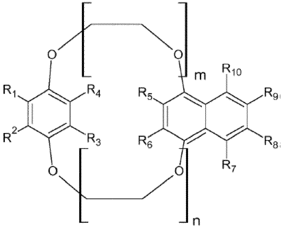
- Composant optoélectronique selon l'une quelconque des revendications précédentes, caractérisé en ce que les éthers-couronnes sont choisis dans un groupe de formule générale (Ia) ou (Ib) :

 où Ar = phényle, biphényle, triphényle, naphtyle, binaphtyle, 3-6 cycles phényle condensés, anthracényle, phénanthrényle, pyrényleHetar = thiophène, pyrrole, furane, oxazole, thiazole, oxadiazole, thiadiazole, triazole, pyridine, pyrimidine, pyrazine, benzothiophènes, benzopyrrole, benzofurane, benzothiophène, benzopyrrole, benzofurane, benzoxazole, benzothiazole, thiénothiophènes, thiénopyrrole, thiénofurane, 3-6 hétérocycles condensés, dithiénothiophène, dithiénopyrrole, dithiénobenzène, dithiénocyclopentadiènes, dipyrrolobenzène
ponts éther en liaison 1,2, 1,3 et 1,4 au cycle phényle (position ortho, méta et para), cycle naphtyle, cycle phényle condensé, ainsi que cycle hétéroaryle et cycle hétéroaryle condensé, respectif,m et n représentent indépendamment l'un de l'autre 1, 2, 3, 4, 5, 6o et p représentent indépendamment l'un de l'autre 0, 1, 2, 3, 4, 5, 6. - Composant optoélectronique selon la revendication 13, caractérisé en ce que les éthers-couronnes sont des composés de structures suivantes :


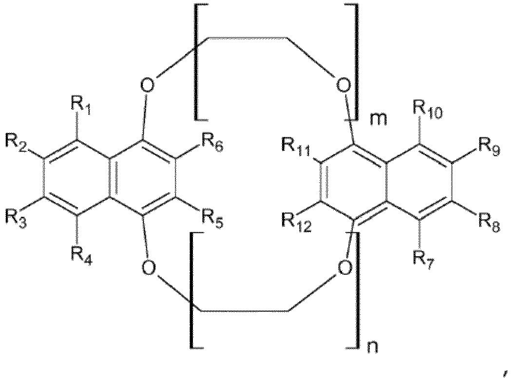 étant entendu qu'en chaque cas : n et m sont choisis indépendamment l'un de l'autre parmi 3, 4 ou 5, etR1, R2, R3, R4, R5, R6, R7, R8, R9, R10, R11 et R12 sont choisis indépendamment les uns des autres parmi H, CH3, C2H5, C3H7, C4H9, C5H11, C6H13, isobutyle, CF3, C2F5, C3F7, C4F9, C5F11, C6F13, OH, O-CH3, CH2-O-CH3, CH2-O-CH2-CH3, CN, phényle, thiophène.
 - Composant optoélectronique selon l'une quelconque des revendications 1 à 12, caractérisé en ce que les éthers-couronnes présentent la formule générale (II) suivante :
 où Ar = phényle, biphényle, triphényle, naphtyle, binaphtyle, 3-6 cycles phényle condensés (anthracényle, phénanthrényle, pyrényle,...)Hetar = thiophène, pyrrole, furane, oxazole, thiazole, oxadiazole, thiadiazole, triazole, pyridine, pyrimidine, pyrazine, benzothiophènes, benzopyrrole, benzofurane, benzothiophène, benzopyrrole, benzofurane, benzoxazole, benzothiazole, thiénothiophènes, thiénopyrrole, thiénofurane, 3-6 hétérocycles condensés, dithiénothiophène, dithiénopyrrole, dithiénobenzène, dithiénocyclopentadiènes, dipyrrolobenzène
ponts éther en liaison 1,2, 1,3 et 1,4 au cycle phényle (position ortho, méta et para), cycle naphtyle, cycle phényle condensé, ainsi que cycle hétéroaryle et cycle hétéroaryle condensé, respectif,m et n représentent indépendamment l'un de l'autre 1, 2, 3, 4, 5, 6p et q représentent indépendamment l'un de l'autre 1, 2, 3, 4, 5, 6. - Utilisation d'éthers-couronnes selon l'une quelconque des revendications 1 à 15 dans des couches photoactives de composants optoélectroniques.
- Composant optoélectronique selon l'une quelconque des revendications précédentes, caractérisé en ce que le composant optoélectronique (1) est une cellule solaire organique.
Applications Claiming Priority (3)
| Application Number | Priority Date | Filing Date | Title |
|---|---|---|---|
| DE102013101715 | 2013-02-21 | ||
| DE201310110373 DE102013110373A1 (de) | 2013-09-19 | 2013-09-19 | Optoelektronisches Bauelement |
| PCT/EP2014/053479 WO2014128278A1 (fr) | 2013-02-21 | 2014-02-21 | Composant optoélectronique |
Publications (2)
| Publication Number | Publication Date |
|---|---|
| EP2959520A1 EP2959520A1 (fr) | 2015-12-30 |
| EP2959520B1 true EP2959520B1 (fr) | 2017-02-01 |
Family
ID=50272573
Family Applications (1)
| Application Number | Title | Priority Date | Filing Date |
|---|---|---|---|
| EP14709574.9A Active EP2959520B1 (fr) | 2013-02-21 | 2014-02-21 | Composant optoélectronique |
Country Status (9)
| Country | Link |
|---|---|
| US (1) | US10950811B2 (fr) |
| EP (1) | EP2959520B1 (fr) |
| JP (1) | JP6329181B2 (fr) |
| KR (1) | KR101972437B1 (fr) |
| CN (1) | CN105308768B (fr) |
| DK (1) | DK2959520T3 (fr) |
| ES (1) | ES2623258T3 (fr) |
| SG (1) | SG10201706775RA (fr) |
| WO (1) | WO2014128278A1 (fr) |
Families Citing this family (9)
| Publication number | Priority date | Publication date | Assignee | Title |
|---|---|---|---|---|
| CN105914297B (zh) * | 2016-04-27 | 2017-04-19 | 扬州鑫晶光伏科技有限公司 | 一种有机光伏电池及其制备方法 |
| CN105837601A (zh) * | 2016-05-03 | 2016-08-10 | 沈荣存 | 一种芳环修饰有机光伏电池及其制备方法 |
| DE102016118177A1 (de) | 2016-09-26 | 2018-03-29 | Heliatek Gmbh | Organisches Bauelement zur Umwandlung von Licht in elektrische Energie mit verbesserter Effizienz und Lebensdauer bei Teilverschattung |
| TWI829640B (zh) * | 2017-07-10 | 2024-01-21 | 美商陶氏有機矽公司 | 可固化聚矽氧組合物及光學半導體裝置 |
| DE202019102792U1 (de) | 2019-05-17 | 2020-05-20 | Heliatek Gmbh | Säule mit mindestens einem photovoltaischen Element und Verwendung eines photovoltaischen Elements an einer Säule |
| DE102019113016A1 (de) * | 2019-05-17 | 2020-11-19 | Heliatek Gmbh | Säule mit mindestens einem photovoltaischen Element und Verwendung eines photovoltaischen Elements an einer Säule |
| DE102019129355A1 (de) | 2019-10-30 | 2021-05-06 | Heliatek Gmbh | Photovoltaisches Element mit verbesserter Effizienz bei Verschattung und Verfahren zur Herstellung eines solchen photovoltaischen Elements |
| DE102019129832A1 (de) | 2019-11-05 | 2021-05-06 | Heliatek Gmbh | Optoelektronisches Bauelement, sowie Verfahren zur Kontaktierung eines optoelektronischen Bauelements |
| EP3890041A1 (fr) | 2020-03-31 | 2021-10-06 | Heliatek GmbH | Nouveaux composés chimiques, éléments optoélectroniques comprenant au moins un nouveau composé chimique et utilisation de nouveaux composés chimiques dans un élément optoélectronique |
Family Cites Families (23)
| Publication number | Priority date | Publication date | Assignee | Title |
|---|---|---|---|---|
| EP0238556A1 (fr) | 1985-09-20 | 1987-09-30 | Kenneth Francis GODWELL | Appareil de vaporisation |
| JP2610861B2 (ja) | 1987-03-09 | 1997-05-14 | 株式会社リコー | 電子写真用感光体 |
| US4863822A (en) | 1987-03-09 | 1989-09-05 | Ricoh Company Ltd. | Electrophotographic photoconductor comprising charge generating and transport layers containing adjuvants |
| KR100977905B1 (ko) | 2003-03-19 | 2010-08-24 | 헬리아텍 게엠베하 | 유기층을 포함하는 광활성 부품 |
| GB0307975D0 (en) * | 2003-04-05 | 2003-05-14 | Univ Cambridge Tech | Composite structure |
| US20050164019A1 (en) | 2004-01-22 | 2005-07-28 | General Electric Company | Charge transfer-promoting materials and electronic devices incorporating same |
| DE102004021989A1 (de) * | 2004-05-04 | 2005-12-15 | Covion Organic Semiconductors Gmbh | Organische elektronische Vorrichtungen |
| DE102005010978A1 (de) | 2005-03-04 | 2006-09-07 | Technische Universität Dresden | Photoaktives Bauelement mit organischen Schichten |
| EP1861881B1 (fr) | 2005-03-21 | 2017-09-06 | Merck Patent GmbH | Cellule photovoltaique polymerique |
| US8053024B2 (en) * | 2005-04-27 | 2011-11-08 | Konica Minolta Holdings, Inc. | Method for manufacturing organic electroluminescent device |
| KR20070080683A (ko) | 2006-02-08 | 2007-08-13 | 삼성전자주식회사 | 광전소자용 전해질 및 이를 채용한 염료감응 태양전지 |
| JP4872805B2 (ja) | 2007-05-28 | 2012-02-08 | パナソニック電工株式会社 | 有機エレクトロルミネッセンス素子 |
| JP5258037B2 (ja) * | 2008-09-08 | 2013-08-07 | 国立大学法人京都大学 | 光電変換素子、その製造方法、及び太陽電池 |
| WO2010084865A1 (fr) * | 2009-01-20 | 2010-07-29 | 東レ株式会社 | Matériau pour élément photovoltaïque, et élément photovoltaïque |
| DK2513995T3 (en) * | 2009-12-16 | 2016-08-29 | Heliatek Gmbh | PHOTOACTIVE COMPONENT WITH ORGANIC LAYERS |
| ES2857904T3 (es) | 2010-05-04 | 2021-09-29 | Heliatek Gmbh | Componente fotoactivo con capas orgánicas |
| WO2011158592A1 (fr) * | 2010-06-18 | 2011-12-22 | コニカミノルタホールディングス株式会社 | Elément électroluminescent organique et procédé de fabrication d'un élément électroluminescent organique |
| DE102010030500A1 (de) | 2010-06-24 | 2011-12-29 | Heliatek Gmbh | Verdampfbares organisch halbleitendes Material und dessen Verwendung in einem optoelektronischen Bauelement |
| EP2400575B1 (fr) | 2010-06-24 | 2016-03-23 | heliatek GmbH | Composant optoélectronique doté de couches organiques |
| DE102010033026B4 (de) | 2010-07-29 | 2014-10-09 | Mainrad Martus | Verfahren zum Aufbau einer als Tandemzelle weitergebildeten organischen Kunststoffsolarzelle |
| WO2012053444A1 (fr) | 2010-10-22 | 2012-04-26 | 住友化学株式会社 | Composé organique présentant une structure cyclique |
| CN102153733B (zh) * | 2011-01-28 | 2012-09-26 | 华南理工大学 | 超分子聚合物光电材料及其应用 |
| TWI480309B (zh) * | 2011-12-06 | 2015-04-11 | Nat Univ Tsing Hua | 具有電洞阻擋功能的高分子與接枝有電子注入/傳遞功能的金屬離子鑲嵌入冠醚側鏈之共軛高分子之複合材料及其於oled及有機太陽能電池的用途 |
-
2014
- 2014-02-21 EP EP14709574.9A patent/EP2959520B1/fr active Active
- 2014-02-21 WO PCT/EP2014/053479 patent/WO2014128278A1/fr active Application Filing
- 2014-02-21 DK DK14709574.9T patent/DK2959520T3/en active
- 2014-02-21 KR KR1020157026006A patent/KR101972437B1/ko active IP Right Grant
- 2014-02-21 SG SG10201706775RA patent/SG10201706775RA/en unknown
- 2014-02-21 ES ES14709574.9T patent/ES2623258T3/es active Active
- 2014-02-21 CN CN201480016298.3A patent/CN105308768B/zh active Active
- 2014-02-21 JP JP2015558471A patent/JP6329181B2/ja active Active
- 2014-02-21 US US14/769,469 patent/US10950811B2/en active Active
Also Published As
| Publication number | Publication date |
|---|---|
| CN105308768A (zh) | 2016-02-03 |
| EP2959520A1 (fr) | 2015-12-30 |
| US10950811B2 (en) | 2021-03-16 |
| KR20150140282A (ko) | 2015-12-15 |
| JP6329181B2 (ja) | 2018-05-23 |
| SG10201706775RA (en) | 2017-09-28 |
| JP2016513371A (ja) | 2016-05-12 |
| ES2623258T3 (es) | 2017-07-10 |
| DK2959520T3 (en) | 2017-05-08 |
| KR101972437B1 (ko) | 2019-04-25 |
| WO2014128278A1 (fr) | 2014-08-28 |
| US20160020419A1 (en) | 2016-01-21 |
| CN105308768B (zh) | 2017-12-29 |
Similar Documents
| Publication | Publication Date | Title |
|---|---|---|
| EP2959520B1 (fr) | Composant optoélectronique | |
| DE102004014046B4 (de) | Photoaktives Bauelement mit organischen Schichten | |
| DE102009051142B4 (de) | Photoaktives Bauelement mit invertierter Schichtfolge und Verfahren zu seiner Herstellung | |
| EP2398056B1 (fr) | Cellule solaire organique dotée de plusieurs systèmes de couches de transport | |
| EP2400575B1 (fr) | Composant optoélectronique doté de couches organiques | |
| WO2010031833A1 (fr) | Utilisation du dibenzotétraphénylpériflanthène dans des cellules solaires organiques | |
| DE202006021034U1 (de) | Organisches photoaktives Bauelement | |
| DE102010030500A1 (de) | Verdampfbares organisch halbleitendes Material und dessen Verwendung in einem optoelektronischen Bauelement | |
| WO2014206860A1 (fr) | Composant semi-conducteur organique | |
| WO2010049512A1 (fr) | Mérocyanines pour la fabrication de couches photoactives pour des cellules solaires organiques et des photodétecteurs organiques | |
| EP2867932A2 (fr) | Électrode transparente pour composants optoélectroniques | |
| DE102009038633B4 (de) | Photoaktives Bauelement mit organischen Doppel- bzw. Mehrfachmischschichten | |
| DE102012104247B4 (de) | Halbleitendes organisches Material für optoelektronische Bauelemente | |
| DE102009024956A1 (de) | Invertierte oder transparente organische Solarzelle oder Photodetektor mit verbesserter Absorption | |
| WO2014006566A1 (fr) | Agencement d'électrodes pour des composants électro-optiques | |
| WO2010139782A1 (fr) | Élément de construction organique absorbant la lumière | |
| EP4271677A1 (fr) | Composé pour composant optoélectronique et composant optoélectronique contenant le composé | |
| DE102019125715A1 (de) | Verbindungen mit einer Furopyrrol- oder einer Thienopyrrolgruppe, optoelektronische Bauelemente mit einer solchen Verbindung, und Verwendung einer solchen Verbindung in optoelektronischen Bauelementen | |
| DE102013110373A1 (de) | Optoelektronisches Bauelement | |
| WO2010133205A1 (fr) | Cellule solaire organique ou photodétecteur à absorption améliorée | |
| WO2021223814A1 (fr) | Système laser pour composant électronique organique | |
| DE102012105809A1 (de) | Transparente Elektrode für optoelektronische Bauelemente | |
| DE102012105810A1 (de) | Transparente Elektrode für optoelektronische Bauelemente | |
| DE102019120457A1 (de) | Organische halbleitende Verbindung mit einer Indolgruppe, organisches optoelektronisches Bauelement mit einer solchen Verbindung, und Verwendung einer solchen Verbindung | |
| WO2012093180A1 (fr) | Composant électronique ou optoélectronique comprenant des couches organiques |
Legal Events
| Date | Code | Title | Description |
|---|---|---|---|
| PUAI | Public reference made under article 153(3) epc to a published international application that has entered the european phase |
Free format text: ORIGINAL CODE: 0009012 |
|
| 17P | Request for examination filed |
Effective date: 20151105 |
|
| AK | Designated contracting states |
Kind code of ref document: A1 Designated state(s): AL AT BE BG CH CY CZ DE DK EE ES FI FR GB GR HR HU IE IS IT LI LT LU LV MC MK MT NL NO PL PT RO RS SE SI SK SM TR |
|
| AX | Request for extension of the european patent |
Extension state: BA ME |
|
| RIN1 | Information on inventor provided before grant (corrected) |
Inventor name: LEVICHKOVA, MARIETA Inventor name: WEISS, ANDRE Inventor name: UHRICH, CHRISTIAN Inventor name: PFEIFFER, MARTIN Inventor name: WALZER, KARSTEN Inventor name: MATTERSTEIG, GUNTER |
|
| DAX | Request for extension of the european patent (deleted) | ||
| GRAP | Despatch of communication of intention to grant a patent |
Free format text: ORIGINAL CODE: EPIDOSNIGR1 |
|
| INTG | Intention to grant announced |
Effective date: 20160901 |
|
| GRAS | Grant fee paid |
Free format text: ORIGINAL CODE: EPIDOSNIGR3 |
|
| GRAA | (expected) grant |
Free format text: ORIGINAL CODE: 0009210 |
|
| AK | Designated contracting states |
Kind code of ref document: B1 Designated state(s): AL AT BE BG CH CY CZ DE DK EE ES FI FR GB GR HR HU IE IS IT LI LT LU LV MC MK MT NL NO PL PT RO RS SE SI SK SM TR |
|
| REG | Reference to a national code |
Ref country code: GB Ref legal event code: FG4D Free format text: NOT ENGLISH |
|
| REG | Reference to a national code |
Ref country code: CH Ref legal event code: EP Ref country code: AT Ref legal event code: REF Ref document number: 866225 Country of ref document: AT Kind code of ref document: T Effective date: 20170215 |
|
| REG | Reference to a national code |
Ref country code: IE Ref legal event code: FG4D Free format text: LANGUAGE OF EP DOCUMENT: GERMAN |
|
| REG | Reference to a national code |
Ref country code: FR Ref legal event code: PLFP Year of fee payment: 4 |
|
| REG | Reference to a national code |
Ref country code: DE Ref legal event code: R096 Ref document number: 502014002624 Country of ref document: DE |
|
| REG | Reference to a national code |
Ref country code: NL Ref legal event code: FP |
|
| REG | Reference to a national code |
Ref country code: DK Ref legal event code: T3 Effective date: 20170502 |
|
| REG | Reference to a national code |
Ref country code: LT Ref legal event code: MG4D |
|
| REG | Reference to a national code |
Ref country code: ES Ref legal event code: FG2A Ref document number: 2623258 Country of ref document: ES Kind code of ref document: T3 Effective date: 20170710 |
|
| PG25 | Lapsed in a contracting state [announced via postgrant information from national office to epo] |
Ref country code: HR Free format text: LAPSE BECAUSE OF FAILURE TO SUBMIT A TRANSLATION OF THE DESCRIPTION OR TO PAY THE FEE WITHIN THE PRESCRIBED TIME-LIMIT Effective date: 20170201 Ref country code: NO Free format text: LAPSE BECAUSE OF FAILURE TO SUBMIT A TRANSLATION OF THE DESCRIPTION OR TO PAY THE FEE WITHIN THE PRESCRIBED TIME-LIMIT Effective date: 20170501 Ref country code: IS Free format text: LAPSE BECAUSE OF FAILURE TO SUBMIT A TRANSLATION OF THE DESCRIPTION OR TO PAY THE FEE WITHIN THE PRESCRIBED TIME-LIMIT Effective date: 20170601 Ref country code: LT Free format text: LAPSE BECAUSE OF FAILURE TO SUBMIT A TRANSLATION OF THE DESCRIPTION OR TO PAY THE FEE WITHIN THE PRESCRIBED TIME-LIMIT Effective date: 20170201 Ref country code: GR Free format text: LAPSE BECAUSE OF FAILURE TO SUBMIT A TRANSLATION OF THE DESCRIPTION OR TO PAY THE FEE WITHIN THE PRESCRIBED TIME-LIMIT Effective date: 20170502 Ref country code: FI Free format text: LAPSE BECAUSE OF FAILURE TO SUBMIT A TRANSLATION OF THE DESCRIPTION OR TO PAY THE FEE WITHIN THE PRESCRIBED TIME-LIMIT Effective date: 20170201 |
|
| PG25 | Lapsed in a contracting state [announced via postgrant information from national office to epo] |
Ref country code: LV Free format text: LAPSE BECAUSE OF FAILURE TO SUBMIT A TRANSLATION OF THE DESCRIPTION OR TO PAY THE FEE WITHIN THE PRESCRIBED TIME-LIMIT Effective date: 20170201 Ref country code: BG Free format text: LAPSE BECAUSE OF FAILURE TO SUBMIT A TRANSLATION OF THE DESCRIPTION OR TO PAY THE FEE WITHIN THE PRESCRIBED TIME-LIMIT Effective date: 20170501 Ref country code: PL Free format text: LAPSE BECAUSE OF FAILURE TO SUBMIT A TRANSLATION OF THE DESCRIPTION OR TO PAY THE FEE WITHIN THE PRESCRIBED TIME-LIMIT Effective date: 20170201 Ref country code: PT Free format text: LAPSE BECAUSE OF FAILURE TO SUBMIT A TRANSLATION OF THE DESCRIPTION OR TO PAY THE FEE WITHIN THE PRESCRIBED TIME-LIMIT Effective date: 20170601 Ref country code: RS Free format text: LAPSE BECAUSE OF FAILURE TO SUBMIT A TRANSLATION OF THE DESCRIPTION OR TO PAY THE FEE WITHIN THE PRESCRIBED TIME-LIMIT Effective date: 20170201 Ref country code: SE Free format text: LAPSE BECAUSE OF FAILURE TO SUBMIT A TRANSLATION OF THE DESCRIPTION OR TO PAY THE FEE WITHIN THE PRESCRIBED TIME-LIMIT Effective date: 20170201 |
|
| PG25 | Lapsed in a contracting state [announced via postgrant information from national office to epo] |
Ref country code: SK Free format text: LAPSE BECAUSE OF FAILURE TO SUBMIT A TRANSLATION OF THE DESCRIPTION OR TO PAY THE FEE WITHIN THE PRESCRIBED TIME-LIMIT Effective date: 20170201 Ref country code: CZ Free format text: LAPSE BECAUSE OF FAILURE TO SUBMIT A TRANSLATION OF THE DESCRIPTION OR TO PAY THE FEE WITHIN THE PRESCRIBED TIME-LIMIT Effective date: 20170201 Ref country code: RO Free format text: LAPSE BECAUSE OF FAILURE TO SUBMIT A TRANSLATION OF THE DESCRIPTION OR TO PAY THE FEE WITHIN THE PRESCRIBED TIME-LIMIT Effective date: 20170201 Ref country code: EE Free format text: LAPSE BECAUSE OF FAILURE TO SUBMIT A TRANSLATION OF THE DESCRIPTION OR TO PAY THE FEE WITHIN THE PRESCRIBED TIME-LIMIT Effective date: 20170201 |
|
| REG | Reference to a national code |
Ref country code: DE Ref legal event code: R097 Ref document number: 502014002624 Country of ref document: DE |
|
| REG | Reference to a national code |
Ref country code: IE Ref legal event code: MM4A |
|
| PG25 | Lapsed in a contracting state [announced via postgrant information from national office to epo] |
Ref country code: SM Free format text: LAPSE BECAUSE OF FAILURE TO SUBMIT A TRANSLATION OF THE DESCRIPTION OR TO PAY THE FEE WITHIN THE PRESCRIBED TIME-LIMIT Effective date: 20170201 Ref country code: MC Free format text: LAPSE BECAUSE OF FAILURE TO SUBMIT A TRANSLATION OF THE DESCRIPTION OR TO PAY THE FEE WITHIN THE PRESCRIBED TIME-LIMIT Effective date: 20170201 |
|
| PLBE | No opposition filed within time limit |
Free format text: ORIGINAL CODE: 0009261 |
|
| STAA | Information on the status of an ep patent application or granted ep patent |
Free format text: STATUS: NO OPPOSITION FILED WITHIN TIME LIMIT |
|
| PG25 | Lapsed in a contracting state [announced via postgrant information from national office to epo] |
Ref country code: LU Free format text: LAPSE BECAUSE OF NON-PAYMENT OF DUE FEES Effective date: 20170221 |
|
| 26N | No opposition filed |
Effective date: 20171103 |
|
| REG | Reference to a national code |
Ref country code: FR Ref legal event code: PLFP Year of fee payment: 5 |
|
| PG25 | Lapsed in a contracting state [announced via postgrant information from national office to epo] |
Ref country code: IE Free format text: LAPSE BECAUSE OF NON-PAYMENT OF DUE FEES Effective date: 20170221 Ref country code: SI Free format text: LAPSE BECAUSE OF FAILURE TO SUBMIT A TRANSLATION OF THE DESCRIPTION OR TO PAY THE FEE WITHIN THE PRESCRIBED TIME-LIMIT Effective date: 20170201 |
|
| PG25 | Lapsed in a contracting state [announced via postgrant information from national office to epo] |
Ref country code: MT Free format text: LAPSE BECAUSE OF FAILURE TO SUBMIT A TRANSLATION OF THE DESCRIPTION OR TO PAY THE FEE WITHIN THE PRESCRIBED TIME-LIMIT Effective date: 20170201 |
|
| PG25 | Lapsed in a contracting state [announced via postgrant information from national office to epo] |
Ref country code: HU Free format text: LAPSE BECAUSE OF FAILURE TO SUBMIT A TRANSLATION OF THE DESCRIPTION OR TO PAY THE FEE WITHIN THE PRESCRIBED TIME-LIMIT; INVALID AB INITIO Effective date: 20140221 |
|
| PG25 | Lapsed in a contracting state [announced via postgrant information from national office to epo] |
Ref country code: CY Free format text: LAPSE BECAUSE OF FAILURE TO SUBMIT A TRANSLATION OF THE DESCRIPTION OR TO PAY THE FEE WITHIN THE PRESCRIBED TIME-LIMIT Effective date: 20170201 |
|
| PG25 | Lapsed in a contracting state [announced via postgrant information from national office to epo] |
Ref country code: MK Free format text: LAPSE BECAUSE OF FAILURE TO SUBMIT A TRANSLATION OF THE DESCRIPTION OR TO PAY THE FEE WITHIN THE PRESCRIBED TIME-LIMIT Effective date: 20170201 |
|
| PG25 | Lapsed in a contracting state [announced via postgrant information from national office to epo] |
Ref country code: TR Free format text: LAPSE BECAUSE OF FAILURE TO SUBMIT A TRANSLATION OF THE DESCRIPTION OR TO PAY THE FEE WITHIN THE PRESCRIBED TIME-LIMIT Effective date: 20170201 |
|
| REG | Reference to a national code |
Ref country code: AT Ref legal event code: MM01 Ref document number: 866225 Country of ref document: AT Kind code of ref document: T Effective date: 20190221 |
|
| PG25 | Lapsed in a contracting state [announced via postgrant information from national office to epo] |
Ref country code: AT Free format text: LAPSE BECAUSE OF NON-PAYMENT OF DUE FEES Effective date: 20190221 |
|
| PG25 | Lapsed in a contracting state [announced via postgrant information from national office to epo] |
Ref country code: AL Free format text: LAPSE BECAUSE OF FAILURE TO SUBMIT A TRANSLATION OF THE DESCRIPTION OR TO PAY THE FEE WITHIN THE PRESCRIBED TIME-LIMIT Effective date: 20170201 |
|
| REG | Reference to a national code |
Ref country code: DE Ref legal event code: R079 Ref document number: 502014002624 Country of ref document: DE Free format text: PREVIOUS MAIN CLASS: H01L0051420000 Ipc: H10K0030000000 |
|
| PGFP | Annual fee paid to national office [announced via postgrant information from national office to epo] |
Ref country code: NL Payment date: 20230222 Year of fee payment: 10 |
|
| PGFP | Annual fee paid to national office [announced via postgrant information from national office to epo] |
Ref country code: FR Payment date: 20230223 Year of fee payment: 10 Ref country code: ES Payment date: 20230321 Year of fee payment: 10 Ref country code: DK Payment date: 20230223 Year of fee payment: 10 Ref country code: CH Payment date: 20230307 Year of fee payment: 10 |
|
| PGFP | Annual fee paid to national office [announced via postgrant information from national office to epo] |
Ref country code: IT Payment date: 20230220 Year of fee payment: 10 Ref country code: GB Payment date: 20230214 Year of fee payment: 10 Ref country code: DE Payment date: 20230227 Year of fee payment: 10 Ref country code: BE Payment date: 20230222 Year of fee payment: 10 |
|
| PGFP | Annual fee paid to national office [announced via postgrant information from national office to epo] |
Ref country code: NL Payment date: 20240226 Year of fee payment: 11 Ref country code: ES Payment date: 20240307 Year of fee payment: 11 |