EP2954101B1 - Method and system for forming a sic crystal - Google Patents
Method and system for forming a sic crystal Download PDFInfo
- Publication number
- EP2954101B1 EP2954101B1 EP13824055.1A EP13824055A EP2954101B1 EP 2954101 B1 EP2954101 B1 EP 2954101B1 EP 13824055 A EP13824055 A EP 13824055A EP 2954101 B1 EP2954101 B1 EP 2954101B1
- Authority
- EP
- European Patent Office
- Prior art keywords
- seed
- crystal
- lid
- graphite
- sic
- Prior art date
- Legal status (The legal status is an assumption and is not a legal conclusion. Google has not performed a legal analysis and makes no representation as to the accuracy of the status listed.)
- Active
Links
Images

Classifications
-
- C—CHEMISTRY; METALLURGY
- C30—CRYSTAL GROWTH
- C30B—SINGLE-CRYSTAL GROWTH; UNIDIRECTIONAL SOLIDIFICATION OF EUTECTIC MATERIAL OR UNIDIRECTIONAL DEMIXING OF EUTECTOID MATERIAL; REFINING BY ZONE-MELTING OF MATERIAL; PRODUCTION OF A HOMOGENEOUS POLYCRYSTALLINE MATERIAL WITH DEFINED STRUCTURE; SINGLE CRYSTALS OR HOMOGENEOUS POLYCRYSTALLINE MATERIAL WITH DEFINED STRUCTURE; AFTER-TREATMENT OF SINGLE CRYSTALS OR A HOMOGENEOUS POLYCRYSTALLINE MATERIAL WITH DEFINED STRUCTURE; APPARATUS THEREFOR
- C30B23/00—Single-crystal growth by condensing evaporated or sublimed materials
- C30B23/02—Epitaxial-layer growth
- C30B23/025—Epitaxial-layer growth characterised by the substrate
-
- C—CHEMISTRY; METALLURGY
- C23—COATING METALLIC MATERIAL; COATING MATERIAL WITH METALLIC MATERIAL; CHEMICAL SURFACE TREATMENT; DIFFUSION TREATMENT OF METALLIC MATERIAL; COATING BY VACUUM EVAPORATION, BY SPUTTERING, BY ION IMPLANTATION OR BY CHEMICAL VAPOUR DEPOSITION, IN GENERAL; INHIBITING CORROSION OF METALLIC MATERIAL OR INCRUSTATION IN GENERAL
- C23C—COATING METALLIC MATERIAL; COATING MATERIAL WITH METALLIC MATERIAL; SURFACE TREATMENT OF METALLIC MATERIAL BY DIFFUSION INTO THE SURFACE, BY CHEMICAL CONVERSION OR SUBSTITUTION; COATING BY VACUUM EVAPORATION, BY SPUTTERING, BY ION IMPLANTATION OR BY CHEMICAL VAPOUR DEPOSITION, IN GENERAL
- C23C14/00—Coating by vacuum evaporation, by sputtering or by ion implantation of the coating forming material
- C23C14/06—Coating by vacuum evaporation, by sputtering or by ion implantation of the coating forming material characterised by the coating material
- C23C14/0635—Carbides
-
- C—CHEMISTRY; METALLURGY
- C23—COATING METALLIC MATERIAL; COATING MATERIAL WITH METALLIC MATERIAL; CHEMICAL SURFACE TREATMENT; DIFFUSION TREATMENT OF METALLIC MATERIAL; COATING BY VACUUM EVAPORATION, BY SPUTTERING, BY ION IMPLANTATION OR BY CHEMICAL VAPOUR DEPOSITION, IN GENERAL; INHIBITING CORROSION OF METALLIC MATERIAL OR INCRUSTATION IN GENERAL
- C23C—COATING METALLIC MATERIAL; COATING MATERIAL WITH METALLIC MATERIAL; SURFACE TREATMENT OF METALLIC MATERIAL BY DIFFUSION INTO THE SURFACE, BY CHEMICAL CONVERSION OR SUBSTITUTION; COATING BY VACUUM EVAPORATION, BY SPUTTERING, BY ION IMPLANTATION OR BY CHEMICAL VAPOUR DEPOSITION, IN GENERAL
- C23C14/00—Coating by vacuum evaporation, by sputtering or by ion implantation of the coating forming material
- C23C14/22—Coating by vacuum evaporation, by sputtering or by ion implantation of the coating forming material characterised by the process of coating
- C23C14/24—Vacuum evaporation
- C23C14/243—Crucibles for source material
-
- C—CHEMISTRY; METALLURGY
- C23—COATING METALLIC MATERIAL; COATING MATERIAL WITH METALLIC MATERIAL; CHEMICAL SURFACE TREATMENT; DIFFUSION TREATMENT OF METALLIC MATERIAL; COATING BY VACUUM EVAPORATION, BY SPUTTERING, BY ION IMPLANTATION OR BY CHEMICAL VAPOUR DEPOSITION, IN GENERAL; INHIBITING CORROSION OF METALLIC MATERIAL OR INCRUSTATION IN GENERAL
- C23C—COATING METALLIC MATERIAL; COATING MATERIAL WITH METALLIC MATERIAL; SURFACE TREATMENT OF METALLIC MATERIAL BY DIFFUSION INTO THE SURFACE, BY CHEMICAL CONVERSION OR SUBSTITUTION; COATING BY VACUUM EVAPORATION, BY SPUTTERING, BY ION IMPLANTATION OR BY CHEMICAL VAPOUR DEPOSITION, IN GENERAL
- C23C14/00—Coating by vacuum evaporation, by sputtering or by ion implantation of the coating forming material
- C23C14/22—Coating by vacuum evaporation, by sputtering or by ion implantation of the coating forming material characterised by the process of coating
- C23C14/24—Vacuum evaporation
- C23C14/26—Vacuum evaporation by resistance or inductive heating of the source
-
- C—CHEMISTRY; METALLURGY
- C23—COATING METALLIC MATERIAL; COATING MATERIAL WITH METALLIC MATERIAL; CHEMICAL SURFACE TREATMENT; DIFFUSION TREATMENT OF METALLIC MATERIAL; COATING BY VACUUM EVAPORATION, BY SPUTTERING, BY ION IMPLANTATION OR BY CHEMICAL VAPOUR DEPOSITION, IN GENERAL; INHIBITING CORROSION OF METALLIC MATERIAL OR INCRUSTATION IN GENERAL
- C23C—COATING METALLIC MATERIAL; COATING MATERIAL WITH METALLIC MATERIAL; SURFACE TREATMENT OF METALLIC MATERIAL BY DIFFUSION INTO THE SURFACE, BY CHEMICAL CONVERSION OR SUBSTITUTION; COATING BY VACUUM EVAPORATION, BY SPUTTERING, BY ION IMPLANTATION OR BY CHEMICAL VAPOUR DEPOSITION, IN GENERAL
- C23C14/00—Coating by vacuum evaporation, by sputtering or by ion implantation of the coating forming material
- C23C14/22—Coating by vacuum evaporation, by sputtering or by ion implantation of the coating forming material characterised by the process of coating
- C23C14/54—Controlling or regulating the coating process
- C23C14/542—Controlling the film thickness or evaporation rate
-
- C—CHEMISTRY; METALLURGY
- C30—CRYSTAL GROWTH
- C30B—SINGLE-CRYSTAL GROWTH; UNIDIRECTIONAL SOLIDIFICATION OF EUTECTIC MATERIAL OR UNIDIRECTIONAL DEMIXING OF EUTECTOID MATERIAL; REFINING BY ZONE-MELTING OF MATERIAL; PRODUCTION OF A HOMOGENEOUS POLYCRYSTALLINE MATERIAL WITH DEFINED STRUCTURE; SINGLE CRYSTALS OR HOMOGENEOUS POLYCRYSTALLINE MATERIAL WITH DEFINED STRUCTURE; AFTER-TREATMENT OF SINGLE CRYSTALS OR A HOMOGENEOUS POLYCRYSTALLINE MATERIAL WITH DEFINED STRUCTURE; APPARATUS THEREFOR
- C30B23/00—Single-crystal growth by condensing evaporated or sublimed materials
- C30B23/002—Controlling or regulating
- C30B23/005—Controlling or regulating flux or flow of depositing species or vapour
-
- C—CHEMISTRY; METALLURGY
- C30—CRYSTAL GROWTH
- C30B—SINGLE-CRYSTAL GROWTH; UNIDIRECTIONAL SOLIDIFICATION OF EUTECTIC MATERIAL OR UNIDIRECTIONAL DEMIXING OF EUTECTOID MATERIAL; REFINING BY ZONE-MELTING OF MATERIAL; PRODUCTION OF A HOMOGENEOUS POLYCRYSTALLINE MATERIAL WITH DEFINED STRUCTURE; SINGLE CRYSTALS OR HOMOGENEOUS POLYCRYSTALLINE MATERIAL WITH DEFINED STRUCTURE; AFTER-TREATMENT OF SINGLE CRYSTALS OR A HOMOGENEOUS POLYCRYSTALLINE MATERIAL WITH DEFINED STRUCTURE; APPARATUS THEREFOR
- C30B23/00—Single-crystal growth by condensing evaporated or sublimed materials
- C30B23/02—Epitaxial-layer growth
- C30B23/06—Heating of the deposition chamber, the substrate or the materials to be evaporated
- C30B23/066—Heating of the material to be evaporated
-
- C—CHEMISTRY; METALLURGY
- C30—CRYSTAL GROWTH
- C30B—SINGLE-CRYSTAL GROWTH; UNIDIRECTIONAL SOLIDIFICATION OF EUTECTIC MATERIAL OR UNIDIRECTIONAL DEMIXING OF EUTECTOID MATERIAL; REFINING BY ZONE-MELTING OF MATERIAL; PRODUCTION OF A HOMOGENEOUS POLYCRYSTALLINE MATERIAL WITH DEFINED STRUCTURE; SINGLE CRYSTALS OR HOMOGENEOUS POLYCRYSTALLINE MATERIAL WITH DEFINED STRUCTURE; AFTER-TREATMENT OF SINGLE CRYSTALS OR A HOMOGENEOUS POLYCRYSTALLINE MATERIAL WITH DEFINED STRUCTURE; APPARATUS THEREFOR
- C30B29/00—Single crystals or homogeneous polycrystalline material with defined structure characterised by the material or by their shape
- C30B29/10—Inorganic compounds or compositions
- C30B29/36—Carbides
-
- H—ELECTRICITY
- H10—SEMICONDUCTOR DEVICES; ELECTRIC SOLID-STATE DEVICES NOT OTHERWISE PROVIDED FOR
- H10P—GENERIC PROCESSES OR APPARATUS FOR THE MANUFACTURE OR TREATMENT OF DEVICES COVERED BY CLASS H10
- H10P90/00—Preparation of wafers not covered by a single main group of this subclass, e.g. wafer reinforcement
- H10P90/12—Preparing bulk and homogeneous wafers
-
- H—ELECTRICITY
- H10—SEMICONDUCTOR DEVICES; ELECTRIC SOLID-STATE DEVICES NOT OTHERWISE PROVIDED FOR
- H10D—INORGANIC ELECTRIC SEMICONDUCTOR DEVICES
- H10D62/00—Semiconductor bodies, or regions thereof, of devices having potential barriers
- H10D62/80—Semiconductor bodies, or regions thereof, of devices having potential barriers characterised by the materials
- H10D62/83—Semiconductor bodies, or regions thereof, of devices having potential barriers characterised by the materials being Group IV materials, e.g. B-doped Si or undoped Ge
- H10D62/832—Semiconductor bodies, or regions thereof, of devices having potential barriers characterised by the materials being Group IV materials, e.g. B-doped Si or undoped Ge being Group IV materials comprising two or more elements, e.g. SiGe
- H10D62/8325—Silicon carbide
-
- Y—GENERAL TAGGING OF NEW TECHNOLOGICAL DEVELOPMENTS; GENERAL TAGGING OF CROSS-SECTIONAL TECHNOLOGIES SPANNING OVER SEVERAL SECTIONS OF THE IPC; TECHNICAL SUBJECTS COVERED BY FORMER USPC CROSS-REFERENCE ART COLLECTIONS [XRACs] AND DIGESTS
- Y10—TECHNICAL SUBJECTS COVERED BY FORMER USPC
- Y10T—TECHNICAL SUBJECTS COVERED BY FORMER US CLASSIFICATION
- Y10T428/00—Stock material or miscellaneous articles
- Y10T428/24—Structurally defined web or sheet [e.g., overall dimension, etc.]
- Y10T428/24273—Structurally defined web or sheet [e.g., overall dimension, etc.] including aperture
Definitions
- the disclosed invention relates to manufacturing of silicon carbide (SiC) crystals and wafers.
- SiC Silicon carbide
- SiC is a crystalline semiconductor material, recognized by those familiar with materials science, electronics and physics as being advantageous for its wide band gap properties and also for extreme hardness, high thermal conductivity and chemical inert properties. These properties make SiC a very attractive semiconductor for fabrication of power semiconductor devices, enabling power density and performance enhancement over devices made from more common materials like silicon.
- SiC consist of cubic or hexagonal arrangements of atoms.
- the stacking of Si and C layers can take on many forms, known as polytypes.
- the type of silicon carbide crystal is denoted by a number denoting the number of repeat units in the stacking sequence followed by a letter representing the crystalline format.
- the 3C-SiC polytype refers to a repeat unit of 3 and a cubic (C) lattice
- a 4H-SiC polytype refers to repeat unit of 4 and a hexagonal (H) lattice.
- the different silicon carbide polytypes have some variations in materials properties, most notably electrical properties.
- the 4H-SiC polytype has the relatively larger bandgap while the 3C-SiC has a smaller bandgap, with the bandgaps for most other polytypes falling in between.
- the material is more capable, in theory, to offer relatively higher power and thermal conductivity performance.
- SiC crystals do not occur in nature and as such must be synthesized. Growth of SiC crystals can be executed by sublimation/physical vapor transport or chemical vapor deposition.
- SiC abrasive materials formed by processes like the Acheson method were used as the source of the Si and C atoms for the crystal, and as the technology matured groups developed means to synthesize SiC source powder specifically for SiC crystal growth.
- the growth is usually performed in a graphite container within a vacuum chamber.
- the graphite container is heated by either resistive methods or induction methods.
- the container is insulated in a careful manner so as to create controlled temperature gradients within the volume.
- a seed crystal is used, which is usually shaped like a plate or disc.
- the seed crystal is typically oriented with its growth surface facing the source material.
- the location of the seed crystal in the container is designed such that when the container is heated, the seed is at a relatively lower temperature position , while the Si-C source materials are at the higher temperature position.
- the container is heated to a temperature sufficient to sublime the source material, the vapors will travel towards the low temperature region and condense on the seed crystal. While this appears simple in concept, in practice the growth of SiC is very complicated and recognized by those who practice as very difficult to perform.
- defects can be categorized as inclusions and crystal dislocations.
- the primary crystalline defects in SiC crystals are screw dislocations. Among these are a special case known as a micropipe or hollow core screw dislocations. Additionally, there are basal plane dislocations and threading edge dislocations. These defects originate from many sources. For example, defects contained in the seed crystal can be passed to the newly grown crystal volume. Stresses arising from temperature gradients and thermal expansion mismatch and imparted to the seed and the crystal during growth can result in formation of dislocations.
- Deviation of the stoichiometry in the sublimation vapor stream from that needed to form SiC can result in unstable polytype growth; in turn leading to polytype inclusions in the grown crystal, which leads to dislocation formation at the polytype boundaries. Even interactions between dislocations can create or eliminate dislocations.
- SiC crystals produced by methods identified have large concentrations of dislocations.
- the commonly reported values of screw dislocation and basal plane concentration are nominally 5,000-10,000/cm 2 , respectively.
- the dislocations are most commonly assessed by sectioning the crystal in the plane normal to the crystal axis of symmetry. Etching the exposed crystal surface with molten salt, like potassium hydroxide, at temperatures in the 350-500°C range will reveal the dislocations.
- molten salt like potassium hydroxide
- Each dislocation type has a unique shape so they can be uniquely counted.
- the dislocations are commonly counted and reported as a number divided by the inspection area. This characterization method is useful as it allows for easy correlation of defects contained in planar semiconductor devices formed on the crystal plane.
- SiC films In order to build semiconductor devices on SiC wafers additional crystalline SiC films must be deposited on the wafers to create the device active regions with the required conductivity value and conductor type. This is typically done using chemical vapor deposition (CVD) methods. Techniques for growth of SiC by CVD epitaxy have been published from groups in Russia, Japan and the United States since the 1970's. The most common chemistry for growth of SiC by CVD is a mixture of a silicon containing source gas (e.g., monosilanes or chlorosilanes) and a carbon containing source gas (e.g., a hydrocarbon gas).
- a silicon containing source gas e.g., monosilanes or chlorosilanes
- a carbon containing source gas e.g., a hydrocarbon gas
- a key element to growth of low defect epitaxial layers is that the substrate surface is tilted away from the crystal axis of symmetry to allow the chemical atoms to attach to the surface in the stacking order established by the substrate crystal.
- the CVD process will produce three dimensional defects on the surface, and such defects will result in non-operational semiconductor devices.
- Surface imperfections such as cracks, subsurface damage, pits, particles, scratches or contamination will interrupt the replication of the wafer's crystal structure by the CVD process (see, for example, Powell and Larkin, Phys. Stat. Sol. (b) 202, 529 (1997 )). It is important that the polishing and cleaning processes used to fabricate the wafer minimize surface imperfections.
- Hull reported shift to lower values in the distribution of high voltage diode reverse bias leakage current when the diodes were fabricated on substrates having lower screw dislocation density ( Hull, et. al., Mat. Sci. forum, Vol. 600-603, p. 931-934 (2009 )).
- Lendenmann reported forward voltage degradation in bipolar diodes was linked to basal plane dislocations in the epilayer that originate from basal plane dislocations in the substrate ( Lendenmann et. al., Mat. Sci. Forum, Vols 338-342, pp. 1161-1166 (2000 )).
- crystals of SiC may be grown by PVT in a reaction cell which is typically formed from solid graphite.
- the cell is typically a right angle cylinder and the grade of graphite is chosen so that its thermal expansion coefficient is close to that of SiC in order to minimize stresses imparted by the differences in the respective coefficients of expansion.
- the SiC seed crystal is typically provided in a disk shape.
- the seed crystal is polished and can be coated on the side opposite the growth surface with a material which is stable at the growth temperatures.
- the presence of a protective carbon coating can help to suppress deterioration of the seed during the crystal growth process, as voids ("thermal evaporation cavities") may form in the seed when the protection is absent.
- the seed is generally oriented in the reaction cell so that the major axis of the cylindrical reaction cell and the plane of the seed wafer are nominally at right angles to each other.
- the seed crystal is placed above the Si/C source feedstock to aid in controlling vapor flow as well as keeping the seed free of debris and contamination during growth.
- the seed is typically supported above the vapor source by rigid or mechanical attachment of the seed to the lid of the reaction cell.
- the seed may be attached to the lid by adhesive, cement, retaining rings, and the like.
- the act of mounting the seed to the reaction cell lid or seed holder can lead to undesirable effects during crystal growth.
- the reaction cell It is important to support the seed crystal in the reaction cell in a position where the temperature can be controlled to allow condensation of the vapor stream on the seed surface.
- the reaction cell is typically made from a different material than the seed crystal, the rigid attachment methods often create stresses in the crystal during growth. For example, when the seeds are mounted to the reaction cell or lid using an adhesive, it is possible for the seed to be bent during the mounting process, which results in undesirable stress in the crystal.
- JP 2011-20860 relies on pressure differentials to create vacuum that holds the seed against the lid.
- contact between the crystal and holder is such that stress on the crystal may still occur during growth.
- pressure differential forces may deform the seed.
- the lid's surface is not smooth and flat, it will create pressure points on the back surface of the seed, thereby generating strains in the seed.
- any particulate material that may inadvertently be captured between the seed and the lid would create pressure point.
- BPD Basal plane dislocation
- US2010295059 describes an SiC single-crystal substrate wherein, when the SiC single-crystal substrate is divided into 5-mm square regions, such regions in which dislocation pairs or dislocation rows have intervals between their dislocation end positions of 5 ⁇ m or less are present among the dislocations that have ends at the substrate surface account for 50% or less of all such regions within the substrate surface and the dislocation density in the substrate of dislocations other than the dislocation pairs or dislocation rows is 8,000/cm 2 .
- US2011206929 provides a single-crystal silicon carbide and a single-crystal silicon carbide wafer that are low in dislocations, micropipes and other crystal defects and enable high yield and high performance when applied to a device, wherein the ratio of doping element concentrations on opposite sides in the direction of crystal growth of the interface between the seed crystal and the grown crystal is 5 or less and the doping element concentration of the grown crystal in the vicinity of the seed crystal is 2x10 19 cm -3 to 6x10 20 cm -3 .
- EP2371997 relates to a method for manufacturing crystals, in particular of silicon carbide, from gaseous phase, said crystals being applicable in high power electronics and optoelectronics as substrate materials for epitaxial structures.
- the method consists in that a monocrystalline seed in a form of a wafer, mounted in a ring of a high purity graphite such that only its edge abuts directly with the ring, is placed in the upper part of the growth chamber filled with an inert gas or with a gas ensuring doping of the crystal, with the feedstock deposited on its bottom, after which the seed is heated up to the crystallization temperature at the condition of a high pressure of the gas filling the chamber and a higher temperature in the lower part of the chamber is maintained while preserving the temperature difference between the feedstock and the seed in the range of 50°C to 300°C.
- a cerium-containing compound is added to the environment of the growth process, in the amount of 0.1g to 10g or in the weight ratio of 0.01% to 1%, with respect to the feedstock.
- US2002083892 describes a method wherein an SiC source material powder and an SiC seed crystal are disposed inside a graphite crucible, and the SiC source material powder is thermally sublimated and recrystallized on a front surface of the SiC seed crystal to grow an SiC single crystal.
- a protection layer is provided on a back surface of the SiC seed crystal.
- the SiC seed crystal is mechanically supported by a supporting part disposed on the graphite crucible.
- JP2012171800 provides a method and an apparatus for producing a silicon carbide single crystal wherein a seed crystal is fixed to a fixing member so that a main surface of the seed crystal is faced to the open part side, and that a main surface of the seed crystal is faced to the bottom part side, and the main surface of a silicon carbide member is faced to the main surface of the seed crystal, and a space S is provided between the main surface of the silicon carbide member and the main surface of the seed crystal, to thereby fix the silicon carbide member.
- the present invention relates to a method of forming an SiC crystal by vapor transport onto a seed crystal; a system for forming an SiC crystal; and a graphite container for use in a furnace for performing SiC crystal growth on a disk-shaped seed having a known diameter; as claimed.
- Preferred embodiments of the invention are set forth in the dependent claims. Associated methods are also described herein to aid in the understanding of the invention, but these do not form part of the claimed invention. Examples or embodiments described herein which do not fall under the definition of the claims do not form part of the present invention
- the seed crystal of the vapor transport growth method is not subjected to external stress during crystal growth.
- Polytype 4H-SiC crystals can be grown using seeds of diameter as small as 76 mm or up to and exceeding 150 mm diameter.
- a 4H-SiC substrate cut from a SiC crystal and having an averaged micropipe density of less than about 1/cm 2 , a screw dislocation density of less than about 5,000/cm 2 , and a basal plane dislocation density of less than about 5,000/cm 2 as determined from at least 9 measurements made on the 4H-SiC substrate.
- the following provides examples of fabrication methods which result in substrates of relatively large diameter while exhibiting low micropipes, screw and basal plane dislocations densities.
- the apparatus and method employed are designed to exert no stress on the seed, so as to limit defects in the grown crystal. No clamping, bonding or mechanical attachments are used to retain the seed in place, and the seed is allowed to thermally expand without constraints, but the vertical movement is limited such that the back surface of the seed is prevented from contacting the surface of the lid.
- the following illustrates how the seed can be retained in place without physically attaching it to the lid, although other examples may be used to achieve the same effect.
- the process begins with an SiC seed, which is generally in the shape of a circular wafer of the same diameter as the grown crystal.
- the seed crystals are polished and or etched on the carbon face to ensure that the surface is free of mechanical damage.
- Methods of the invention provide several advantages over prior art methods and apparatus for seed crystal growth.
- Most prior art methods connect the seed with contact between the back surface of the seed and the top of the crucible or reaction cell/lid.
- we have found that such contact is unnecessary and may be detrimental to crystal formation.
- This configuration of the support minimizes damage to or bending of the seed crystal during the mounting process, and because the seed crystal is mechanically decoupled from the reaction cell, the seed crystal may expand and contract independently of the reaction cell during growth.
- Fig. 1 shows a generic arrangement for growth of SiC crystals by physical vapor transport, indicative of the prior art.
- PVT reaction cell 40 having lid 43 is illustrated which is configured for SiC crystal growth.
- the reaction cell is typically formed from a graphite vessel.
- Granulized SiC or silicon and carbon material 42 is placed in the bottom of the cell.
- a seed crystal 48 mounted to the inside of the top of the cell, e.g, clamped or bonded to lid 43.
- the back surface of the seed 48 contacts the bottom surface of the lid 43, whether by physical attachment, such as adhesive or clamp, or by pressure differential, as explained in JP 2011-20860 .
- the entire vessel is surrounded with insulation 54 such as graphite felt or foam.
- the reaction cell 40 is placed in a vacuum furnace 70 which is pumped by a vacuum pump.
- the vacuum furnace 70 may be comprised of steel if the cell is resistively heated, or it may be comprised of glass if the cell is inductively heated. In the examples shown, the vacuum furnace is comprised of glass and is heated by an RF induction coil 72. Silicon and carbon evaporate from the source material 42 and condense onto the seed 48. Silicon and carbon that has not condensed onto the seed is diffused out of the reaction vessel and into the vacuum furnace. This diffusion is driven by pressure gradient between the interior of the reaction vessel and the vacuum furnace. Gases that are being injected into the vacuum furnace, such as nitrogen, argon, and dopants, diffuse through the graphite crucible walls and into the reaction vessel. This diffusion is driven by concentration gradient between the vacuum chamber and the interior of the reaction vessel.
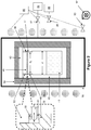
- the reaction cell 40 is preferably formed from a graphite vessel and has lid 43. Granulized SiC or silicon and carbon material 42 is placed in the bottom of the cell.
- the cell has an interior diameter designated as "d” in Figure 2 , which is equal to or larger than the diameter of the seed 48.
- a shelf 46 is provided in the upper portion of the cell. The shelf 46 has an inner diameter, designated "d s " in Figure 2 , which is slightly smaller than the diameter of the seed 48.
- the walls of the shelf need not be vertical, but instead may be slanted, as shown by the dotted line, in which case the diameter "d s " can have a larger value on the source side of the shelf than on the seed side.
- the shelf 46 can be made as a ring of graphite bonded to the sidewall of the vessel.
- the shelf 46 is made integrally with the vessel, e.g., the vessel may be formed with the shelf as integrated part of the interior sidewall of the vessel 40.
- Support 46 is used for supporting the seed crystal 48 at its peripheral edge, without any physical attachment. Rather, cushion rings 50, 51 are placed above and or below the seed, contacting the upper and lower surface of the seed 48 at its periphery.
- the cushion rings allow the seed to flex and expand while keeping the seed in the desired location relative to the cell and prevent the seed from physically contacting the lid 43 throughout the growth process.
- the cushion rings may be made of material that is softer than SiC, is malleable, and can withstand the process conditions and chemical reactions associated with SiC crystal growth. For example, molybdenum or graphite can be used to fabricate the cushion rings 50 and 51.
- a graphite retainer, 53 is positioned above the upper cushion ring 50, so as to maintain the seed's vertical position and prevent the seed from contacting the lid.
- the upper ring 50 and retainer ring 53 need not press on the seed, but rather should allow free movement of the seed in the horizontal direction, as illustrated by the double-headed arrow in the callout. That is, the bottom cushion ring 51 is placed on the shelf 46, the seed 48 is then placed on top of the bottom cushion ring 51 and the top cushion ring 50 is placed on top of the seed 48. The retainer ring 53 is placed over the top cushion ring 50 and then the lid 43 is attached to the cell 40.
- This overall arrangement allows the seed to be in a controlled vertical position, and yet be free to expand and contract without creating stress in the seed upon heating and cooling.
- Finite element modeling shows that this geometrical arrangement to position the seed will correspond to a maximum stress in a bulk SiC crystal of less than 5 ⁇ 10 6 dynes/cm 2 .
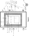
- Figure 3 illustrates another embodiment for forming the shelf 46 as integral part of the cell 40.
- the cell 40 is fabricated such that its interior diameter is slightly smaller than that of the seed 48, similar to diameter d s in the embodiment of Figure 2 .
- the upper part of the cell 40 is fabricated to have a diameter that is slightly larger than the diameter of seed 48, i.e., similar to diameter d in the embodiment of Figure 2 .
- the difference between the two diameters forms shelf 46, upon which the bottom cushion ring 51 rests.
- various configuration can be used to facilitate the shelf 46, and the particular configuration used is not essential, provided that the seed can be placed with the cushion rings on the shelf, such that the seed can expand and contract freely without having horizontal physical constraints, while at the same time preventing the seed rom physically contacting the surface of the lid 43.
- the embodiment of Figure 3 also illustrates making the retainer ring 53 as integral part of the lid 43.
- the lid 43 is fabricated with a protruding ring 53, serving to limit the vertical motion of the cushion ring 50, and thereby limiting the vertical motion of the seed 48.
- the ring 53 may directly contact the peripheral edge of the seed 48, or it may contact the cushion ring 50, when cushion ring 50 is used.
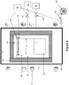
- Figure 4 illustrates yet another embodiment for supporting seed 48 without imparting stresses and enabling free expansion and contraction.
- the shelve 46 is fabricated close to the top opening of the cell 40, such that the retainer is not needed. Instead, the lid 43 serves to restrict the vertical motion of the upper cushion ring 50 by contacting the cushion ring 50, such that the seed cannot contact the surface of the lid 43.
- Another feature shown in Figure 4 is the upper cushion ring 50 being thicker than the bottom cushion ring 51. This is done in order to keep the seed 48 sufficiently far from the lid 43 and reduce the thermal influence of the lid 43 on the seed 48.
- the entire vessel is surrounded with insulation 54 such as graphite felt or foam.
- insulation 54 such as graphite felt or foam.
- the thickness, thermal conductivity, and porosity of the insulation are chosen so as to achieve a desired temperature distribution in the reaction cell.
- the arrangement for growth of SiC crystals can include a controller 80 for controlling a valve 82 to dopant gas, e.g., a nitrogen source 84, which is connected to the vacuum furnace 70, and for controlling a valve 86 to an argon source 88, also connected to the vacuum furnace 70.
- the vacuum inside vacuum furnace 70 is controlled by valve 90 leading to vacuum pump 92.
- controller 80 is configured to control vacuum valve 90 and pump 92 so as to maintain a user-set vacuum level inside the vacuum furnace 70, regardless of argon and/or nitrogen flow into the vacuum furnace. For example, if nitrogen flow into the chamber is increased, controller 80 opens the vacuum valve 90 to increase vacuum pumping from the furnace and maintain the set vacuum level. Controller 80 also controls the operation of the heater, such as the power applied to RF induction coil 72.
- the cell 40 is loaded with the source material 42 and seed 48, it is sealed and is placed into an RF induction furnace 70.
- the furnace is evacuated using pump 92, thereby creating a pressure differential between the interior of the furnace 70 and the interior of the cell 40.
- cell 40 is constructed such that the lid does not seal the cell fully hermetically and so, gaseous matter from inside the cell 40 leaks to the interior of furnace 70 and is pumped out.
- the walls of cell 40 are somewhat porous to gases and leak into the interior of furnace 70. Consequently, the pumping action of pump 92 also evacuates the interior of cell 40 by creating the pressure differential between the interior of cell 40 and the interior of furnace 70.
- furnace 70 is backfilled with a non oxidizing gas such as argon from argon source 88.
- a non oxidizing gas such as argon from argon source 88.
- Pressure is established near atmospheric pressure (500-700 torr) by controlling vacuum valve 90, and the container is heated to approximately 1,600-2,500°C by energizing coils 72.
- the pressure is subsequently reduced to initiate the vapor transport process.
- the pressure is first reduced to the range of 10-100 torr.
- Nitrogen gas can be added to the furnace to control the conductivity of the grown crystal, but regardless of nitrogen flow, the controller maintains the pressure at the set value, i.e., in the range of 10-100 torr.
- the pressure, temperature and nitrogen flow are controlled to achieve the conditions needed to form the bulk SiC crystal on the seed.
- the thickness of the remaining crystal grown is in the range of 5-50 mm. Typical values of pressure are in the range of 0.1-10.0 torr and temperature in the range of 2,000-2,500°C.
- the pressure is raised to approximately 600 torr. This suppresses any more vapor transport.
- the furnace is then cooled to room temperature. When the container is opened, a single crystal of SiC with the same polytype as the seed crystal has formed on the seed crystal.
- New seeds can be created by slicing the crystals grown by this method, and the new seeds can be used to grow new crystals. It is found that each generation of crystals grown shows reduced dislocation density.
- the method disclosed herein involve holding a seed in a vapor transport reaction cell such that the stress imparted to the SiC crystal during growth is minimized to less than 5 ⁇ 10 6 dynes/cm 2 and, as such, the method can be integrated into any strategy to grow large crystals, e.g., having diameter larger than 76 mm and length longer than 25 mm.
- Micropipes can be tested by first revealing them with molten salt etching and counting via manual and automated methods, or by scanning the polished slice with a laser light scattering spectrometer and an image processing algorithm to count the micropipes. Methods such as this are described in J. Wan, et. al., "A New Method of Mapping and Counting Micropipes in SiC Wafers" Proc. 2005 Int'l Conf. On SiC and Related Materials, Materials Science Forum (2006), p. 447 , and J.
- Screw dislocations and basal plane dislocations require either molten salt etching as described above or x-ray topography.
- Counting is generally done by sampling several areas on the slice and counting the defects.
- the method typically used to report defects consists of a measurement at the center of the wafer, four sites 90 degrees apart at 50% of the wafer radius and four sites 90 degrees apart at >80% of the wafer radius, and rotated 45 degrees to the points at 50% of the radius. The total counts in each site are summed, and then the sum is divided by the measurement area to derive a defect density in counts per unit area. Since the sampling method of larger wafers is important to assessing the wafer, it is often pertinent to report the site count values as well as the net count of defects
- a graphite vessel was formed and loaded with a source mixture of silicon and carbon totaling approximately 800 grams.
- a 4H-SiC seed of approximately 70 mm diameter was fixtured into the cell per the methods described earlier with the C-face facing the source.
- the graphite assembly was wrapped with graphite felt and placed into a RF induction heated vacuum furnace.
- the vacuum chamber was evacuated to base pressure and then backfilled with argon gas.
- the pressure was set to 600 T and the system was heated to achieve a temperature of approximately 2200°C as read by a pyrometer focused on the lid of the graphite vessel.
- N2 gas was delivered to the chamber at this time and the pressure was dropped below 10 T to initiate sublimation of the source.
- the N2 gas flow was set to a level to deliver a nitrogen concentration in the crystal within the range 3-8E18/cm 3 . After about 100 hrs the pressure was raised to 600 T to stop sublimation and then the system was cooled to retrieve the crystal.
- the resulting crystal designated BH9013, was 19 mm long on the tapered side. Crystal was sliced into wafers which were offcut 4 degrees toward ⁇ 11-20> and the wafers were polished using diamond abrasives to achieve a smooth specular surface.
- Resistivity measurements performed on the wafers shows the values in the crystal ranged 0.016-0.026 ohm-cm.
- One of the slices was etched in molten KOH to reveal the dislocations.
- Micropipes were measured by counting all the micropipes on the wafer and dividing by the wafer area . In this case 10 micropipes were identified and this corresponds to a micropipe density of 0.12/cm 2 .
- Dislocations were measured at 9 sites on the wafer arranged by radius and angle. The test locations consists of a measurement at the center of the wafer, four sites 90 degrees apart at 50% of the wafer radius and four sites 90 degrees apart at >80% of the wafer radius, and rotated 45 degrees to the points at 50% of the radius.
Landscapes
- Chemical & Material Sciences (AREA)
- Engineering & Computer Science (AREA)
- Materials Engineering (AREA)
- Metallurgy (AREA)
- Organic Chemistry (AREA)
- Crystallography & Structural Chemistry (AREA)
- Chemical Kinetics & Catalysis (AREA)
- Mechanical Engineering (AREA)
- Inorganic Chemistry (AREA)
- Crystals, And After-Treatments Of Crystals (AREA)
Description
- This application claims priority benefit from
U.S. Patent Application Serial Number 14/058,167, filed on October 18, 2013 andU.S. Provisional Patent Application Serial Number 61/761,171, filed on February 5, 2013 - The disclosed invention relates to manufacturing of silicon carbide (SiC) crystals and wafers.
- Silicon carbide, SiC, is a crystalline semiconductor material, recognized by those familiar with materials science, electronics and physics as being advantageous for its wide band gap properties and also for extreme hardness, high thermal conductivity and chemical inert properties. These properties make SiC a very attractive semiconductor for fabrication of power semiconductor devices, enabling power density and performance enhancement over devices made from more common materials like silicon.
- The most common forms of SiC consist of cubic or hexagonal arrangements of atoms. The stacking of Si and C layers can take on many forms, known as polytypes. The type of silicon carbide crystal is denoted by a number denoting the number of repeat units in the stacking sequence followed by a letter representing the crystalline format. For example the 3C-SiC polytype refers to a repeat unit of 3 and a cubic (C) lattice, while a 4H-SiC polytype refers to repeat unit of 4 and a hexagonal (H) lattice.
- The different silicon carbide polytypes have some variations in materials properties, most notably electrical properties. The 4H-SiC polytype has the relatively larger bandgap while the 3C-SiC has a smaller bandgap, with the bandgaps for most other polytypes falling in between. For high performance power device applications when the bandgap is larger, the material is more capable, in theory, to offer relatively higher power and thermal conductivity performance.
- SiC crystals do not occur in nature and as such must be synthesized. Growth of SiC crystals can be executed by sublimation/physical vapor transport or chemical vapor deposition.
- Growth of SiC by sublimation is very challenging. Temperatures in excess of 2,000°C are required to generate vapor stream of Si/ C species by sublimation, which places great limitations on the reaction cell components and the furnace design. Originally SiC abrasive materials formed by processes like the Acheson method were used as the source of the Si and C atoms for the crystal, and as the technology matured groups developed means to synthesize SiC source powder specifically for SiC crystal growth. The growth is usually performed in a graphite container within a vacuum chamber. The graphite container is heated by either resistive methods or induction methods. The container is insulated in a careful manner so as to create controlled temperature gradients within the volume. A seed crystal is used, which is usually shaped like a plate or disc. The seed crystal is typically oriented with its growth surface facing the source material. The location of the seed crystal in the container is designed such that when the container is heated, the seed is at a relatively lower temperature position , while the Si-C source materials are at the higher temperature position. When the container is heated to a temperature sufficient to sublime the source material, the vapors will travel towards the low temperature region and condense on the seed crystal. While this appears simple in concept, in practice the growth of SiC is very complicated and recognized by those who practice as very difficult to perform.
- Historically, initial progress in SiC sublimation-based crystal growth is described first by Lely (
US 2,854,364 ) whose method of unseeded crystal growth resulted in small hexagonal SiC platelets. In the 1970s and 1980s the art to produce the first crystals of size attractive for producing devices was done in Russia by Tairov and Tsvetkov (Journal of Crystal Growth, 52 (1981) p. 146-50 and Progress in Controlling the Growth of Polytypic Crystals in Crystal Growth and Characterization of Polytype Structures, P. Krishna, ed., Pergammon Press, London, p. 111 (1983)). Their approach used a Lely crystal as a seed, and conducted growth by sublimation and transport as described above. These results showed methods for polytype control by choice of seeds, pressure control and temperature gradients. Later, Davis (US 4,866,005 ) revealed improvements by judicious selection of source materials and gradient controls. Refinements on the methods of Tairov, Tsvetkov and Davis continue to be revealed to this day. - When methods to produce larger crystals emerged, focus also moved to control defects in the crystals. Defects can be categorized as inclusions and crystal dislocations. The primary crystalline defects in SiC crystals are screw dislocations. Among these are a special case known as a micropipe or hollow core screw dislocations. Additionally, there are basal plane dislocations and threading edge dislocations. These defects originate from many sources. For example, defects contained in the seed crystal can be passed to the newly grown crystal volume. Stresses arising from temperature gradients and thermal expansion mismatch and imparted to the seed and the crystal during growth can result in formation of dislocations. Deviation of the stoichiometry in the sublimation vapor stream from that needed to form SiC can result in unstable polytype growth; in turn leading to polytype inclusions in the grown crystal, which leads to dislocation formation at the polytype boundaries. Even interactions between dislocations can create or eliminate dislocations.
- SiC crystals produced by methods identified have large concentrations of dislocations. As of this filing, the commonly reported values of screw dislocation and basal plane concentration are nominally 5,000-10,000/cm2, respectively. The dislocations are most commonly assessed by sectioning the crystal in the plane normal to the crystal axis of symmetry. Etching the exposed crystal surface with molten salt, like potassium hydroxide, at temperatures in the 350-500°C range will reveal the dislocations. Each dislocation type has a unique shape so they can be uniquely counted. The dislocations are commonly counted and reported as a number divided by the inspection area. This characterization method is useful as it allows for easy correlation of defects contained in planar semiconductor devices formed on the crystal plane. There are many examples in the literature which show that dislocations are not uniformly distributed in the plane of observation. The large count of dislocations makes it very impractical to count every single one, especially as today inspections can be required on sections greater than or equal to the equivalent of 100 mm diameter circles. So the etched area is sampled to determine the amount of dislocations. Incorrect sampling methods can lead to errors in the estimation of the dislocation concentration associated with larger crystals. In most reports, the details of the sampling method are not provided, so replication of reported results can often be difficult, if not impossible.
- Scientists experienced in solid state physics and semiconductor devices know that dislocations result in device performance below the theoretical properties of the material. Therefore, modern effort focused on improvements of semiconductor SiC crystal quality look to identify and control the factors which can reduce defects originating in crystal growth.
- Once large enough crystals are produced, the crystal must be cut and fabricated into wafers in order to be useful to fabricate semiconductor devices using planar fabrication methods. As many semiconductor crystals (e.g., silicon, gallium arsenide) have been successfully developed and commercialized into wafer products, the methods to fabricate wafers from bulk crystals are known. A review of the common approaches to, and requirements for wafer fabrication and standard methods of characterization, can be found in Wolf and Tauber, Silicon Processing for the VLSI Era, Vol.1 - Process Technology, Chapter 1 (Lattice Press -1986).
- Due to its hardness, fabrication of SiC into wafer substrates presents unique challenges compared to processing other common semiconductor crystals like silicon or gallium arsenide. Modifications must be made to the machines and the choices of abrasives changed beyond commonly used materials. It has been reported that substantial subsurface damage is observable on mirror polished SiC wafers, and this can be reduced or removed by using chemical enhanced mechanical polishing methods similar to that used in the silicon industry (Zhou, L., et al., Chemomechanical Polishing of Silicon Carbide, J. Electrochem. Soc., Vol. 144, no. 6, June 1997, pp. L161-L163).
- In order to build semiconductor devices on SiC wafers additional crystalline SiC films must be deposited on the wafers to create the device active regions with the required conductivity value and conductor type. This is typically done using chemical vapor deposition (CVD) methods. Techniques for growth of SiC by CVD epitaxy have been published from groups in Russia, Japan and the United States since the 1970's. The most common chemistry for growth of SiC by CVD is a mixture of a silicon containing source gas (e.g., monosilanes or chlorosilanes) and a carbon containing source gas (e.g., a hydrocarbon gas). A key element to growth of low defect epitaxial layers is that the substrate surface is tilted away from the crystal axis of symmetry to allow the chemical atoms to attach to the surface in the stacking order established by the substrate crystal. When the tilt is not adequate, the CVD process will produce three dimensional defects on the surface, and such defects will result in non-operational semiconductor devices. Surface imperfections, such as cracks, subsurface damage, pits, particles, scratches or contamination will interrupt the replication of the wafer's crystal structure by the CVD process (see, for example, Powell and Larkin, Phys. Stat. Sol. (b) 202, 529 (1997)). It is important that the polishing and cleaning processes used to fabricate the wafer minimize surface imperfections. In the presence of these surface imperfections several defects can be generated in the epitaxial films including basal plane dislocations and cubic SiC inclusions (see for example, Powell, et. al. Transactions Third International High-Temperature Electronics Conference, Volume 1, pp. II-3 - II-8, Sandia National Laboratories, Albuquerque, NM USA, 9-14 June 1996).
- Defects in SiC are known to limit or destroy operation of semiconductor devices formed over the defects. Neudeck and Powell reported that hollow core screw dislocations (micropipes) severely limited voltage blocking performance in SiC diodes (P. G. Neudeck and J. A. Powell, IEEE Electron Device Letters, vol. 15, no. 2, pp. 63-65, (1994)). Neudeck reviewed the impact of crystal (wafer) and epitaxy originated defects on power devices in 1994, highlighting limitations of power device function due to screw dislocations and morphological epitaxy defects (Neudeck, Mat. Sci. Forum, Vols 338-342, pp. 1161-1166 (2000)). Hull reported shift to lower values in the distribution of high voltage diode reverse bias leakage current when the diodes were fabricated on substrates having lower screw dislocation density (Hull, et. al., Mat. Sci. forum, Vol. 600-603, p. 931-934 (2009)). Lendenmann reported forward voltage degradation in bipolar diodes was linked to basal plane dislocations in the epilayer that originate from basal plane dislocations in the substrate (Lendenmann et. al., Mat. Sci. Forum, Vols 338-342, pp. 1161-1166 (2000)).
- Modern technology for growth of 4H-SiC crystals has not been successful to develop a commercial method for a crystal growth process that allows simultaneous control over the gamut of dislocation types.
- Various methods disclosed in the prior art are often lacking in details regarding the specific steps employed in the crystal growth or the methods employed to assess the concentration of defects and demonstrate repeatability.
- In recent years, it has become desirable to grow larger crystals as silicon carbide and gallium nitride as such materials which are useful in building high efficiency power/RF diodes and transistor devices. However, large bulk crystals of silicon carbide (SiC) are difficult to grow, in part because such processes require high temperatures of up to 2,500°C. Currently, most growth processes utilize vapor-based transport methods such as physical vapor transport (PVT) sublimation methods.
- For example, crystals of SiC may be grown by PVT in a reaction cell which is typically formed from solid graphite. The cell is typically a right angle cylinder and the grade of graphite is chosen so that its thermal expansion coefficient is close to that of SiC in order to minimize stresses imparted by the differences in the respective coefficients of expansion. The SiC seed crystal is typically provided in a disk shape. The seed crystal is polished and can be coated on the side opposite the growth surface with a material which is stable at the growth temperatures. The presence of a protective carbon coating can help to suppress deterioration of the seed during the crystal growth process, as voids ("thermal evaporation cavities") may form in the seed when the protection is absent.
- The seed is generally oriented in the reaction cell so that the major axis of the cylindrical reaction cell and the plane of the seed wafer are nominally at right angles to each other. In most PVT reaction cells, the seed crystal is placed above the Si/C source feedstock to aid in controlling vapor flow as well as keeping the seed free of debris and contamination during growth. In this type of PVT reaction cell arrangement, the seed is typically supported above the vapor source by rigid or mechanical attachment of the seed to the lid of the reaction cell. The seed may be attached to the lid by adhesive, cement, retaining rings, and the like. However, the act of mounting the seed to the reaction cell lid or seed holder can lead to undesirable effects during crystal growth.
- For example, during the mounting process, scratching of the coated seed back may occur. In addition, a void may be created between the seed and reaction cell ceiling interface during the mounting process. Such occurrences may exacerbate formation of evaporation cavities of the seed backside, resulting in defect formation. Moreover, differences in thermal expansion between the seed and lid can cause stresses in the seed. See, for example, discussion in Japanese patent publication
JP 2011-20860 - It is important to support the seed crystal in the reaction cell in a position where the temperature can be controlled to allow condensation of the vapor stream on the seed surface. However, because the reaction cell is typically made from a different material than the seed crystal, the rigid attachment methods often create stresses in the crystal during growth. For example, when the seeds are mounted to the reaction cell or lid using an adhesive, it is possible for the seed to be bent during the mounting process, which results in undesirable stress in the crystal.
- As a result, attempts have been made to develop alternative methods for supporting the seed crystal during growth. For example,
JP 2011-20860 - There are other problems with the approach disclosed in the
JP 2011-20860 - Accordingly, there is a need in the art for a method of SiC crystal growth, which results in crystal growth with minimized stress resulting in reduced defects such as micropipes, screw dislocations and basal plane dislocations.
- The following documents may be useful in the understanding of the invention. CHEN W ET AL, "Growth and characterization of 4H-SiC epilayers on substrates with different off-cut angles", JOURNAL OF APPLIED PHYSICS, vol. 98, no. 11, page 114907 investigates epitaxial growth on 4H-SiC (0001) substrates with 4° and 8° off-cut angles. Both growth rate and nitrogen doping show a dependence on the C/Si ratio and off-cut angle. Good surface morphologies were obtained on the 8° off-angle substrates over a wide range of C/Si ratios, while macrostep bunching was observed on the 4° off-angle substrates depending on C/Si ratios. Step bunching behaviors on both substrate orientations were investigated by Nomarski microscopy and atomic force microscopy, and possible step bunching mechanisms were proposed to explain the results. Basal plane dislocation (BPD) densities were examined by means of molten KOH etching. Low off-cut angle was found to enhance the conversion of BPDs into threading edge dislocations. A BPD density of 2.6 cm-2 was achieved on the 4° off-angle substrate under optimized growth conditions. The effects of changing the C/Si ratio on BPD densities were also investigated.
US2010295059 describes an SiC single-crystal substrate wherein, when the SiC single-crystal substrate is divided into 5-mm square regions, such regions in which dislocation pairs or dislocation rows have intervals between their dislocation end positions of 5 µm or less are present among the dislocations that have ends at the substrate surface account for 50% or less of all such regions within the substrate surface and the dislocation density in the substrate of dislocations other than the dislocation pairs or dislocation rows is 8,000/cm2.US2011206929 provides a single-crystal silicon carbide and a single-crystal silicon carbide wafer that are low in dislocations, micropipes and other crystal defects and enable high yield and high performance when applied to a device, wherein the ratio of doping element concentrations on opposite sides in the direction of crystal growth of the interface between the seed crystal and the grown crystal is 5 or less and the doping element concentration of the grown crystal in the vicinity of the seed crystal is 2x1019 cm-3 to 6x1020 cm-3.EP2371997 relates to a method for manufacturing crystals, in particular of silicon carbide, from gaseous phase, said crystals being applicable in high power electronics and optoelectronics as substrate materials for epitaxial structures. The method consists in that a monocrystalline seed in a form of a wafer, mounted in a ring of a high purity graphite such that only its edge abuts directly with the ring, is placed in the upper part of the growth chamber filled with an inert gas or with a gas ensuring doping of the crystal, with the feedstock deposited on its bottom, after which the seed is heated up to the crystallization temperature at the condition of a high pressure of the gas filling the chamber and a higher temperature in the lower part of the chamber is maintained while preserving the temperature difference between the feedstock and the seed in the range of 50°C to 300°C. Preferably, a cerium-containing compound is added to the environment of the growth process, in the amount of 0.1g to 10g or in the weight ratio of 0.01% to 1%, with respect to the feedstock.US2002083892 describes a method wherein an SiC source material powder and an SiC seed crystal are disposed inside a graphite crucible, and the SiC source material powder is thermally sublimated and recrystallized on a front surface of the SiC seed crystal to grow an SiC single crystal. In this sublimation-recrystallization method, a protection layer is provided on a back surface of the SiC seed crystal. The SiC seed crystal is mechanically supported by a supporting part disposed on the graphite crucible.JP2012171800 - The following summary of the invention is included in order to provide a basic understanding of the invention.
- The present invention relates to a method of forming an SiC crystal by vapor transport onto a seed crystal; a system for forming an SiC crystal; and a graphite container for use in a furnace for performing SiC crystal growth on a disk-shaped seed having a known diameter; as claimed. Preferred embodiments of the invention are set forth in the dependent claims. Associated methods are also described herein to aid in the understanding of the invention, but these do not form part of the claimed invention. Examples or embodiments described herein which do not fall under the definition of the claims do not form part of the present invention
- The seed crystal of the vapor transport growth method is not subjected to external stress during crystal growth.
- Also discussed are methods to produce a 4H-SiC crystal/wafer with micropipe density of less than 1/cm2, screw dislocation density of less than 5,000/cm2 and basal plane dislocation density of less than 5,000/cm2. All the defect metrics are achieved simultaneously.
- Polytype 4H-SiC crystals can be grown using seeds of diameter as small as 76 mm or up to and exceeding 150 mm diameter.
- Also disclosed herein is a 4H-SiC substrate cut from a SiC crystal and having an averaged micropipe density of less than about 1/cm2, a screw dislocation density of less than about 5,000/cm2, and a basal plane dislocation density of less than about 5,000/cm2 as determined from at least 9 measurements made on the 4H-SiC substrate.
- The invention is further described below with reference to the following drawings.
- The accompanying drawings, which are incorporated in and constitute a part of this specification, and together with the description, serve to explain and illustrate the invention. The drawings are intended to illustrate major features of the exemplary embodiments in a diagrammatic manner. The drawings are not intended to depict every feature of actual embodiments nor relative dimensions of the depicted elements, and are not drawn to scale.
-
Fig. 1 shows a generic arrangement for growth of SiC crystals by physical vapor transport, indicative of the prior art. -
Fig. 2 shows a physical vapor transport PVT reaction cell, which is configured for SiC crystal growth according to one embodiment. -
Fig. 3 shows a PVT reaction cell, which is configured for SiC crystal growth according to another embodiment. -
Fig. 4 shows a PVT reaction cell, which is configured for SiC crystal growth according to yet another embodiment. - The following provides examples of fabrication methods which result in substrates of relatively large diameter while exhibiting low micropipes, screw and basal plane dislocations densities. The apparatus and method employed are designed to exert no stress on the seed, so as to limit defects in the grown crystal. No clamping, bonding or mechanical attachments are used to retain the seed in place, and the seed is allowed to thermally expand without constraints, but the vertical movement is limited such that the back surface of the seed is prevented from contacting the surface of the lid. The following illustrates how the seed can be retained in place without physically attaching it to the lid, although other examples may be used to achieve the same effect.
- The process begins with an SiC seed, which is generally in the shape of a circular wafer of the same diameter as the grown crystal. The seed crystals are polished and or etched on the carbon face to ensure that the surface is free of mechanical damage.
- Methods of the invention provide several advantages over prior art methods and apparatus for seed crystal growth. Most prior art methods connect the seed with contact between the back surface of the seed and the top of the crucible or reaction cell/lid. However, we have found that such contact is unnecessary and may be detrimental to crystal formation. We have unexpectedly found that by supporting a seed crystal in a configuration in which the seed is contacted only at its periphery, the stresses imparted to the crystal during growth are minimized. We have also unexpectedly found an improvement in the quality of the grown crystal as evidenced by the low crystal defect density.
- This configuration of the support minimizes damage to or bending of the seed crystal during the mounting process, and because the seed crystal is mechanically decoupled from the reaction cell, the seed crystal may expand and contract independently of the reaction cell during growth.
-
Fig. 1 shows a generic arrangement for growth of SiC crystals by physical vapor transport, indicative of the prior art.PVT reaction cell 40 havinglid 43 is illustrated which is configured for SiC crystal growth. The reaction cell is typically formed from a graphite vessel. Granulized SiC or silicon andcarbon material 42 is placed in the bottom of the cell. Positioned in the upper portion of the vessel is aseed crystal 48 mounted to the inside of the top of the cell, e.g, clamped or bonded tolid 43. Notably, in the configuration ofFigure 1 , during processing the back surface of theseed 48 contacts the bottom surface of thelid 43, whether by physical attachment, such as adhesive or clamp, or by pressure differential, as explained inJP 2011-20860 - The entire vessel is surrounded with
insulation 54 such as graphite felt or foam. Thereaction cell 40 is placed in avacuum furnace 70 which is pumped by a vacuum pump. Thevacuum furnace 70 may be comprised of steel if the cell is resistively heated, or it may be comprised of glass if the cell is inductively heated. In the examples shown, the vacuum furnace is comprised of glass and is heated by anRF induction coil 72. Silicon and carbon evaporate from thesource material 42 and condense onto theseed 48. Silicon and carbon that has not condensed onto the seed is diffused out of the reaction vessel and into the vacuum furnace. This diffusion is driven by pressure gradient between the interior of the reaction vessel and the vacuum furnace. Gases that are being injected into the vacuum furnace, such as nitrogen, argon, and dopants, diffuse through the graphite crucible walls and into the reaction vessel. This diffusion is driven by concentration gradient between the vacuum chamber and the interior of the reaction vessel. - Referring now to
Fig. 2 , a PVT reaction cell according to the invention is illustrated, which is configured for low-stress, low-defect, SiC crystal growth. Thereaction cell 40 is preferably formed from a graphite vessel and haslid 43. Granulized SiC or silicon andcarbon material 42 is placed in the bottom of the cell. The cell has an interior diameter designated as "d" inFigure 2 , which is equal to or larger than the diameter of theseed 48. Additionally, ashelf 46 is provided in the upper portion of the cell. Theshelf 46 has an inner diameter, designated "ds" inFigure 2 , which is slightly smaller than the diameter of theseed 48. Of course, the walls of the shelf need not be vertical, but instead may be slanted, as shown by the dotted line, in which case the diameter "ds" can have a larger value on the source side of the shelf than on the seed side. Whilst not in accordance with the invention, theshelf 46 can be made as a ring of graphite bonded to the sidewall of the vessel. In accordance with the invention, theshelf 46 is made integrally with the vessel, e.g., the vessel may be formed with the shelf as integrated part of the interior sidewall of thevessel 40. -
Shelf 46 is used for supporting theseed crystal 48 at its peripheral edge, without any physical attachment. Rather, cushion rings 50, 51 are placed above and or below the seed, contacting the upper and lower surface of theseed 48 at its periphery. The cushion rings allow the seed to flex and expand while keeping the seed in the desired location relative to the cell and prevent the seed from physically contacting thelid 43 throughout the growth process. The cushion rings may be made of material that is softer than SiC, is malleable, and can withstand the process conditions and chemical reactions associated with SiC crystal growth. For example, molybdenum or graphite can be used to fabricate the cushion rings 50 and 51. Optionally, a graphite retainer, 53, is positioned above theupper cushion ring 50, so as to maintain the seed's vertical position and prevent the seed from contacting the lid. However, it should be appreciated that theupper ring 50 andretainer ring 53 need not press on the seed, but rather should allow free movement of the seed in the horizontal direction, as illustrated by the double-headed arrow in the callout. That is, thebottom cushion ring 51 is placed on theshelf 46, theseed 48 is then placed on top of thebottom cushion ring 51 and thetop cushion ring 50 is placed on top of theseed 48. Theretainer ring 53 is placed over thetop cushion ring 50 and then thelid 43 is attached to thecell 40. This overall arrangement allows the seed to be in a controlled vertical position, and yet be free to expand and contract without creating stress in the seed upon heating and cooling. Finite element modeling shows that this geometrical arrangement to position the seed will correspond to a maximum stress in a bulk SiC crystal of less than 5 × 10⁶ dynes/cm2. -
Figure 3 illustrates another embodiment for forming theshelf 46 as integral part of thecell 40. Specifically, thecell 40 is fabricated such that its interior diameter is slightly smaller than that of theseed 48, similar to diameter ds in the embodiment ofFigure 2 . The upper part of thecell 40 is fabricated to have a diameter that is slightly larger than the diameter ofseed 48, i.e., similar to diameter d in the embodiment ofFigure 2 . The difference between the twodiameters forms shelf 46, upon which thebottom cushion ring 51 rests. Thus, as can be understood, various configuration can be used to facilitate theshelf 46, and the particular configuration used is not essential, provided that the seed can be placed with the cushion rings on the shelf, such that the seed can expand and contract freely without having horizontal physical constraints, while at the same time preventing the seed rom physically contacting the surface of thelid 43. - The embodiment of
Figure 3 also illustrates making theretainer ring 53 as integral part of thelid 43. Specifically, as illustrated inFigure 3 , thelid 43 is fabricated with a protrudingring 53, serving to limit the vertical motion of thecushion ring 50, and thereby limiting the vertical motion of theseed 48. Thering 53 may directly contact the peripheral edge of theseed 48, or it may contact thecushion ring 50, whencushion ring 50 is used. -
Figure 4 illustrates yet another embodiment for supportingseed 48 without imparting stresses and enabling free expansion and contraction. Specifically, theshelve 46 is fabricated close to the top opening of thecell 40, such that the retainer is not needed. Instead, thelid 43 serves to restrict the vertical motion of theupper cushion ring 50 by contacting thecushion ring 50, such that the seed cannot contact the surface of thelid 43. Another feature shown inFigure 4 is theupper cushion ring 50 being thicker than thebottom cushion ring 51. This is done in order to keep theseed 48 sufficiently far from thelid 43 and reduce the thermal influence of thelid 43 on theseed 48. - The following description is applicable regardless of the specific embodiment utilized. The entire vessel is surrounded with
insulation 54 such as graphite felt or foam. The thickness, thermal conductivity, and porosity of the insulation are chosen so as to achieve a desired temperature distribution in the reaction cell. The arrangement for growth of SiC crystals can include acontroller 80 for controlling avalve 82 to dopant gas, e.g., anitrogen source 84, which is connected to thevacuum furnace 70, and for controlling avalve 86 to anargon source 88, also connected to thevacuum furnace 70. The vacuum insidevacuum furnace 70 is controlled byvalve 90 leading tovacuum pump 92. In this embodiment,controller 80 is configured to controlvacuum valve 90 and pump 92 so as to maintain a user-set vacuum level inside thevacuum furnace 70, regardless of argon and/or nitrogen flow into the vacuum furnace. For example, if nitrogen flow into the chamber is increased,controller 80 opens thevacuum valve 90 to increase vacuum pumping from the furnace and maintain the set vacuum level.Controller 80 also controls the operation of the heater, such as the power applied toRF induction coil 72. - Once the
cell 40 is loaded with thesource material 42 andseed 48, it is sealed and is placed into anRF induction furnace 70. The furnace is evacuated usingpump 92, thereby creating a pressure differential between the interior of thefurnace 70 and the interior of thecell 40. However,cell 40 is constructed such that the lid does not seal the cell fully hermetically and so, gaseous matter from inside thecell 40 leaks to the interior offurnace 70 and is pumped out. Similarly, the walls ofcell 40 are somewhat porous to gases and leak into the interior offurnace 70. Consequently, the pumping action ofpump 92 also evacuates the interior ofcell 40 by creating the pressure differential between the interior ofcell 40 and the interior offurnace 70. - Once the interior of
cell 40 andfurnace 70 have been evacuated, the interior offurnace 70 is backfilled with a non oxidizing gas such as argon fromargon source 88. Pressure is established near atmospheric pressure (500-700 torr) by controllingvacuum valve 90, and the container is heated to approximately 1,600-2,500°C by energizingcoils 72. - The pressure is subsequently reduced to initiate the vapor transport process. In this method, the pressure is first reduced to the range of 10-100 torr. Nitrogen gas can be added to the furnace to control the conductivity of the grown crystal, but regardless of nitrogen flow, the controller maintains the pressure at the set value, i.e., in the range of 10-100 torr.
- At this point, the pressure, temperature and nitrogen flow are controlled to achieve the conditions needed to form the bulk SiC crystal on the seed. The thickness of the remaining crystal grown is in the range of 5-50 mm. Typical values of pressure are in the range of 0.1-10.0 torr and temperature in the range of 2,000-2,500°C.
- At the end of the growth process, the pressure is raised to approximately 600 torr. This suppresses any more vapor transport. The furnace is then cooled to room temperature. When the container is opened, a single crystal of SiC with the same polytype as the seed crystal has formed on the seed crystal.
- New seeds can be created by slicing the crystals grown by this method, and the new seeds can be used to grow new crystals. It is found that each generation of crystals grown shows reduced dislocation density.
- As can be appreciated from the above, the method disclosed herein involve holding a seed in a vapor transport reaction cell such that the stress imparted to the SiC crystal during growth is minimized to less than 5 × 10⁶ dynes/cm2 and, as such, the method can be integrated into any strategy to grow large crystals, e.g., having diameter larger than 76 mm and length longer than 25 mm.
- To assess the dislocations in the crystal, the crystal is sliced and all slices are polished. Micropipes can be tested by first revealing them with molten salt etching and counting via manual and automated methods, or by scanning the polished slice with a laser light scattering spectrometer and an image processing algorithm to count the micropipes. Methods such as this are described in J. Wan, et. al., "A New Method of Mapping and Counting Micropipes in SiC Wafers" Proc. 2005 Int'l Conf. On SiC and Related Materials, Materials Science Forum (2006), p. 447, and J. Wan, et, al., "A Comparative Study of Micropipe Decoration and Counting in Conductive and Semi-Insulating Silicon Carbide Wafers," J. Electronic Materials, Vol. 34 (10), p. 1342. Once the total number of defects is counted, this value is divided by the area of the slice measured to derive a defect density in counts per unit area.
- Screw dislocations and basal plane dislocations require either molten salt etching as described above or x-ray topography. Counting is generally done by sampling several areas on the slice and counting the defects. The method typically used to report defects consists of a measurement at the center of the wafer, four
sites 90 degrees apart at 50% of the wafer radius and foursites 90 degrees apart at >80% of the wafer radius, and rotated 45 degrees to the points at 50% of the radius. The total counts in each site are summed, and then the sum is divided by the measurement area to derive a defect density in counts per unit area. Since the sampling method of larger wafers is important to assessing the wafer, it is often pertinent to report the site count values as well as the net count of defects - A graphite vessel was formed and loaded with a source mixture of silicon and carbon totaling approximately 800 grams. A 4H-SiC seed of approximately 70 mm diameter was fixtured into the cell per the methods described earlier with the C-face facing the source. The graphite assembly was wrapped with graphite felt and placed into a RF induction heated vacuum furnace. The vacuum chamber was evacuated to base pressure and then backfilled with argon gas. The pressure was set to 600 T and the system was heated to achieve a temperature of approximately 2200°C as read by a pyrometer focused on the lid of the graphite vessel. N2 gas was delivered to the chamber at this time and the pressure was dropped below 10 T to initiate sublimation of the source. The N2 gas flow was set to a level to deliver a nitrogen concentration in the crystal within the range 3-8E18/cm3. After about 100 hrs the pressure was raised to 600 T to stop sublimation and then the system was cooled to retrieve the crystal.
- The resulting crystal, designated BH9013, was 19 mm long on the tapered side. Crystal was sliced into wafers which were offcut 4 degrees toward <11-20> and the wafers were polished using diamond abrasives to achieve a smooth specular surface.
- Resistivity measurements performed on the wafers shows the values in the crystal ranged 0.016-0.026 ohm-cm.
- One of the slices was etched in molten KOH to reveal the dislocations. Micropipes were measured by counting all the micropipes on the wafer and dividing by the wafer area . In this case 10 micropipes were identified and this corresponds to a micropipe density of 0.12/cm2. Dislocations were measured at 9 sites on the wafer arranged by radius and angle. The test locations consists of a measurement at the center of the wafer, four
sites 90 degrees apart at 50% of the wafer radius and foursites 90 degrees apart at >80% of the wafer radius, and rotated 45 degrees to the points at 50% of the radius. Microscope images were taken at each site and the etch pit density ((EPD) which is the sum of all threading, basal and screw dislocations), basal plane dislocation density and screw dislocation density were determined from the images. The data is tabulated below:Site EPD (cm-2) Basal Plane Dislocation Density (cm-2) Screw Dislocation Density (cm-2) 1 1.25E+03 0 0 2 2.00E+04 500 0 3 2.50E+03 0 0 4 6.00E+03 250 0 5 1.50E+03 250 500 6 5.00E+03 0 0 7 5.25E+03 500 0 8 4.50E+03 0 0 9 0.00E+00 0 0
Claims (11)
- A method of forming an SiC crystal by vapor transport onto a seed crystal (48), the method comprising:a. providing a graphite container (40) having a sidewall and a shelf (46) made as integrated part of interior of the sidewall, and placing a source of silicon and carbon atoms (42) in the graphite container (40), wherein the source of silicon and carbon atoms is for transport to the seed crystal (48) to grow the SiC crystal;b. placing the seed crystal (48) in the graphite container (40), and supporting the seed crystal (48) on the shelf (46) within the graphite container without physically attaching the seed crystal to any part of the graphite container;c. placing a lid (43) over the container such that the lid does not contact the seed crystal, and without physically attaching the seed to the lid, so as to allow free movement of the seed in the horizontal direction such that the seed is free to expand and contract upon heating and cooling, and placing the graphite container in a vacuum furnace (70);d. evacuating the furnace and establishing a flow of inert gas, and controlling the pressure at a value > 79993.4 Pascal (600 torr)e. heating the furnace to a temperature from 2,000°C to about 2,500°C;f. evacuating the furnace to a pressure from 1333.22 Pascal (10 Torr) to about 13332.2 Pascal (100 Torr);g. controlling the pressure from 13.3322 and 13332.2 Pascal (0.1 and 100 torr)h. maintaining the furnace to support crystal growth to thereby form the SiC crystal, while preventing the seed from contacting the lid throughout the crystal growth process.
- The method of claim 1, further comprising flowing nitrogen gas into the furnace.
- The method of claim 2, wherein the furnace is maintained to support crystal growth to thereby form the SiC crystal having a thickness of about 0.1 mm to about 50 mm, and wherein nitrogen flow is maintained such that nitrogen concentration of the grown SiC crystal is from 1 × 10¹⁵/cm3 to 1 × 10¹⁹/cm3.
- The method of claim 1, wherein the seed crystal is a 4H-SiC crystal having an offcut of 0 to 4 degrees toward (11-20) crystal orientation and wherein the nitrogen concentration of the seed crystal is from 1 × 10¹⁶/cm3 to 8 × 10¹⁸/cm3.
- The method of claim 1, further comprising placing a cushion ring (51) between the shelf and the seed, placing a cushion ring between the seed and the lid (50), or placing a cushion ring between the seed and the lid and between the shelf and the seed.
- The method of claim 1 or 5, wherein preventing the seed from contacting the lid comprises placing a retaining ring (53) between the seed and the lid.
- A system for forming an SiC crystal, the system comprising:a. a graphite container (40) having a lid (43) and a shelf (46) for positioning a seed (48) thereupon;b. cushion rings (50), (51), made of molybdenum or graphite, allowing the seed to flex and expand while preventing the seed from contacting the lid;c. a heater (72) for heating an induction furnace to a temperature from 2,000°C to 2,500°C;d. a pump (92) for evacuating the induction furnace to a pressure from 13.3322 Pascal (0.1 Torr) to > 79993.4 Pascal (600 Torr); ande. gas inlet (86) for filling the induction furnace with an inert gas.
- The system of claim 7, wherein the cushion rings comprise a first cushion ring (51) positioned below the seed and a second cushion ring (50) positioned above the seed and a graphite retaining ring positioned above the second cushion ring.
- The system of claim 8, wherein the lid comprises a graphite retaining ring (53) extending from bottom surface of the lid.
- A graphite container for use in a furnace for performing SiC crystal growth on a disk-shaped seed having a known diameter, comprising:a graphite cylindrical container (40) having a sidewall and an open top configured for accepting a graphite lid;a cylindrical shelf (46) formed on an upper part of the sidewall and which is made as integrated part of interior of the sidewall, the cylindrical shelf being formed at a defined distance below the open top, thereby enabling placing and supporting the seed thereupon;a graphite lid (43) configured for forming a closure with the open top; and,means (50), (53) for preventing the seed from contacting the lid.
- The graphite container of claim 10, wherein the means (50), (53) for preventing the seed from contacting the lid comprises a graphite retaining ring.
Applications Claiming Priority (3)
| Application Number | Priority Date | Filing Date | Title |
|---|---|---|---|
| US201361761171P | 2013-02-05 | 2013-02-05 | |
| US14/058,167 US9797064B2 (en) | 2013-02-05 | 2013-10-18 | Method for growing a SiC crystal by vapor deposition onto a seed crystal provided on a support shelf which permits thermal expansion |
| PCT/US2013/077285 WO2014123635A1 (en) | 2013-02-05 | 2013-12-20 | Sic crystal and wafer cut from crystal with low dislocation density |
Publications (2)
| Publication Number | Publication Date |
|---|---|
| EP2954101A1 EP2954101A1 (en) | 2015-12-16 |
| EP2954101B1 true EP2954101B1 (en) | 2020-02-19 |
Family
ID=51259444
Family Applications (1)
| Application Number | Title | Priority Date | Filing Date |
|---|---|---|---|
| EP13824055.1A Active EP2954101B1 (en) | 2013-02-05 | 2013-12-20 | Method and system for forming a sic crystal |
Country Status (6)
| Country | Link |
|---|---|
| US (2) | US9797064B2 (en) |
| EP (1) | EP2954101B1 (en) |
| JP (1) | JP6663548B2 (en) |
| KR (1) | KR102137672B1 (en) |
| CN (2) | CN111676513A (en) |
| WO (1) | WO2014123635A1 (en) |
Cited By (4)
| Publication number | Priority date | Publication date | Assignee | Title |
|---|---|---|---|---|
| EP4617409A1 (en) * | 2024-03-11 | 2025-09-17 | SiCrystal GmbH | Production method for sic bulk single crystal |
| DE112014004073B4 (en) | 2013-09-06 | 2026-04-30 | Gtat Corporation | Sublimation oven |
| DE112014004088B4 (en) | 2013-09-06 | 2026-05-13 | Gtat Corporation | Process for the formation of silicon carbide |
| DE112014004096B4 (en) * | 2013-09-06 | 2026-05-13 | Gtat Corporation | Process for the production of bulk silicon carbide |
Families Citing this family (45)
| Publication number | Priority date | Publication date | Assignee | Title |
|---|---|---|---|---|
| US8860040B2 (en) | 2012-09-11 | 2014-10-14 | Dow Corning Corporation | High voltage power semiconductor devices on SiC |
| US9797064B2 (en) | 2013-02-05 | 2017-10-24 | Dow Corning Corporation | Method for growing a SiC crystal by vapor deposition onto a seed crystal provided on a support shelf which permits thermal expansion |
| US9738991B2 (en) | 2013-02-05 | 2017-08-22 | Dow Corning Corporation | Method for growing a SiC crystal by vapor deposition onto a seed crystal provided on a supporting shelf which permits thermal expansion |
| US9919972B2 (en) | 2013-05-02 | 2018-03-20 | Melior Innovations, Inc. | Pressed and self sintered polymer derived SiC materials, applications and devices |
| US9657409B2 (en) | 2013-05-02 | 2017-05-23 | Melior Innovations, Inc. | High purity SiOC and SiC, methods compositions and applications |
| US11091370B2 (en) | 2013-05-02 | 2021-08-17 | Pallidus, Inc. | Polysilocarb based silicon carbide materials, applications and devices |
| US10322936B2 (en) | 2013-05-02 | 2019-06-18 | Pallidus, Inc. | High purity polysilocarb materials, applications and processes |
| US10403509B2 (en) * | 2014-04-04 | 2019-09-03 | The Government Of The United States Of America, As Represented By The Secretary Of The Navy | Basal plane dislocation elimination in 4H—SiC by pulsed rapid thermal annealing |
| US9279192B2 (en) | 2014-07-29 | 2016-03-08 | Dow Corning Corporation | Method for manufacturing SiC wafer fit for integration with power device manufacturing technology |
| US10753010B2 (en) | 2014-09-25 | 2020-08-25 | Pallidus, Inc. | Vapor deposition apparatus and techniques using high puritiy polymer derived silicon carbide |
| CN105658846B (en) * | 2014-09-30 | 2018-08-28 | 昭和电工株式会社 | The manufacturing method of silicon carbide single crystal wafer and single-crystal silicon carbide ingot |
| KR102478709B1 (en) * | 2014-12-19 | 2022-12-16 | 타타 스틸 네덜란드 테크날러지 베.뷔. | Filter device to remove particles from a vapour stream |
| JP6668674B2 (en) * | 2015-10-15 | 2020-03-18 | 住友電気工業株式会社 | Silicon carbide substrate |
| JP6597381B2 (en) * | 2016-02-22 | 2019-10-30 | 住友電気工業株式会社 | Method for manufacturing silicon carbide substrate, method for manufacturing silicon carbide epitaxial substrate, and method for manufacturing silicon carbide semiconductor device |
| US11339498B2 (en) * | 2016-12-20 | 2022-05-24 | Senic Inc. | Method for growing single crystal silicon carbide ingot having large diameter |
| CN106894089B (en) * | 2017-03-09 | 2018-03-09 | 中科钢研节能科技有限公司 | The preparation method of single-crystal silicon carbide |
| EP3382068B1 (en) * | 2017-03-29 | 2022-05-18 | SiCrystal GmbH | Silicon carbide substrate and method of growing sic single crystal boules |
| KR20250113525A (en) | 2017-03-29 | 2025-07-25 | 팔리두스, 인크. | Sic volumetric shapes and methods of forming boules |
| JP7012518B2 (en) * | 2017-11-24 | 2022-01-28 | 昭和電工株式会社 | SiC epitaxial growth device |
| JP7422479B2 (en) * | 2017-12-22 | 2024-01-26 | 株式会社レゾナック | SiC ingot and method for producing SiC ingot |
| CN109137076A (en) * | 2018-10-17 | 2019-01-04 | 福建北电新材料科技有限公司 | A kind of fixed device of seed wafer and its application method of growth single-crystal silicon carbide |
| US11680340B2 (en) * | 2018-12-13 | 2023-06-20 | Axt, Inc. | Low etch pit density 6 inch semi-insulating gallium arsenide wafers |
| CN109825882A (en) * | 2019-02-18 | 2019-05-31 | 国宏中晶集团有限公司 | A kind of annealing device and method of silicon carbide electric-resistivity method growth crystal |
| CN109913949A (en) * | 2019-02-18 | 2019-06-21 | 国宏中晶集团有限公司 | A kind of thermal field simulation system of silicon carbide electric-resistivity method growth crystal |
| CN109898139A (en) * | 2019-02-18 | 2019-06-18 | 国宏中晶集团有限公司 | A kind of material processing device and method of silicon carbide electric-resistivity method growth crystal |
| JP7393900B2 (en) * | 2019-09-24 | 2023-12-07 | 一般財団法人電力中央研究所 | Method for manufacturing silicon carbide single crystal wafer and silicon carbide single crystal ingot |
| KR102340110B1 (en) | 2019-10-29 | 2021-12-17 | 주식회사 쎄닉 | Silicon carbide ingot, wafer and manufacturing method of the same |
| CN111321472B (en) * | 2020-03-25 | 2022-02-22 | 哈尔滨科友半导体产业装备与技术研究院有限公司 | Device and method for accurately expanding AlN seed crystals |
| CN113512758B (en) * | 2020-04-09 | 2024-07-05 | 赛尼克公司 | Silicon carbide ingot and method for manufacturing the same, and system for manufacturing the silicon carbide ingot |
| KR102235858B1 (en) | 2020-04-09 | 2021-04-02 | 에스케이씨 주식회사 | Manufacturing method for silicon carbide ingot and system for manufacturing silicon carbide ingot |
| CN113174631A (en) * | 2020-06-05 | 2021-07-27 | 北京世纪金光半导体有限公司 | High-thickness low-defect six-inch silicon carbide crystal growth method meeting industrial production |
| DE102020117661A1 (en) | 2020-07-03 | 2022-01-20 | Friedrich-Alexander-Universität Erlangen-Nürnberg | Crystal growing facility for the production of a single crystal |
| US11987902B2 (en) * | 2020-07-27 | 2024-05-21 | Globalwafers Co., Ltd. | Manufacturing method of silicon carbide wafer and semiconductor structure |
| CN112430845B (en) * | 2020-11-26 | 2022-07-08 | 山东天岳先进科技股份有限公司 | Silicon carbide single crystal and production method and application thereof |
| CN112609238B (en) * | 2020-11-26 | 2022-11-29 | 山东天岳先进科技股份有限公司 | Crucible, device and application for growth of N-type silicon carbide single crystal |
| CN112626619B (en) * | 2020-11-26 | 2022-07-12 | 山东天岳先进科技股份有限公司 | Silicon carbide single crystal ingot, substrate and preparation method thereof |
| CN112466929B (en) * | 2020-11-26 | 2023-04-28 | 山东天岳先进科技股份有限公司 | Silicon carbide substrate, ingot and preparation method thereof |
| CN112501687B (en) * | 2020-11-26 | 2022-07-12 | 山东天岳先进科技股份有限公司 | Silicon carbide wafer, crystal ingot and preparation method thereof |
| CN112501694B (en) * | 2020-11-26 | 2022-07-08 | 山东天岳先进科技股份有限公司 | Silicon carbide wafer, ingot and preparation method thereof |
| WO2022110634A1 (en) * | 2020-11-26 | 2022-06-02 | 山东天岳先进科技股份有限公司 | Silicon carbide single crystal wafer and ingot, and preparation method therefor |
| JP7494768B2 (en) * | 2021-03-16 | 2024-06-04 | 信越半導体株式会社 | Method for evaluating crystal defects in silicon carbide single crystal wafers |
| EP4060098A1 (en) | 2021-03-19 | 2022-09-21 | SiCrystal GmbH | Method for producing sic-volume single crystal of inhomogeneous screw dislocation distribution and sic substrate |
| CN113652751B (en) * | 2021-08-19 | 2022-04-19 | 福建北电新材料科技有限公司 | Crystal growth apparatus and crystal growth method |
| US11971216B1 (en) | 2021-12-23 | 2024-04-30 | Rolls-Royce High Temperature Composites, Inc. | Retort with loading window |
| KR102858294B1 (en) | 2022-03-04 | 2025-09-11 | 서울대학교병원 | Survival information prediction system for lung disease patient using chest radiographic image and survival information prediction method |
Citations (1)
| Publication number | Priority date | Publication date | Assignee | Title |
|---|---|---|---|---|
| JP2012171800A (en) * | 2011-02-17 | 2012-09-10 | Bridgestone Corp | Method and apparatus for producing silicon carbide single crystal |
Family Cites Families (253)
| Publication number | Priority date | Publication date | Assignee | Title |
|---|---|---|---|---|
| NL87348C (en) | 1954-03-19 | 1900-01-01 | ||
| US3691694A (en) | 1970-11-02 | 1972-09-19 | Ibm | Wafer polishing machine |
| US4582561A (en) | 1979-01-25 | 1986-04-15 | Sharp Kabushiki Kaisha | Method for making a silicon carbide substrate |
| US4866005A (en) | 1987-10-26 | 1989-09-12 | North Carolina State University | Sublimation of silicon carbide to produce large, device quality single crystals of silicon carbide |
| US4912064A (en) | 1987-10-26 | 1990-03-27 | North Carolina State University | Homoepitaxial growth of alpha-SiC thin films and semiconductor devices fabricated thereon |
| US4912063A (en) | 1987-10-26 | 1990-03-27 | North Carolina State University | Growth of beta-sic thin films and semiconductor devices fabricated thereon |
| JP2534525B2 (en) | 1987-12-19 | 1996-09-18 | 富士通株式会社 | Method for manufacturing β-silicon carbide layer |
| JPH0831419B2 (en) | 1990-12-25 | 1996-03-27 | 名古屋大学長 | Method for producing compound semiconductor single crystal on single crystal silicon substrate |
| JP2804860B2 (en) | 1991-04-18 | 1998-09-30 | 新日本製鐵株式会社 | SiC single crystal and growth method thereof |
| US5192987A (en) | 1991-05-17 | 1993-03-09 | Apa Optics, Inc. | High electron mobility transistor with GaN/Alx Ga1-x N heterojunctions |
| US5248385A (en) | 1991-06-12 | 1993-09-28 | The United States Of America, As Represented By The Administrator, National Aeronautics And Space Administration | Process for the homoepitaxial growth of single-crystal silicon carbide films on silicon carbide wafers |
| US5149338A (en) | 1991-07-22 | 1992-09-22 | Fulton Kenneth W | Superpolishing agent, process for polishing hard ceramic materials, and polished hard ceramics |
| US5238532A (en) | 1992-02-27 | 1993-08-24 | Hughes Aircraft Company | Method and apparatus for removal of subsurface damage in semiconductor materials by plasma etching |
| US5709745A (en) | 1993-01-25 | 1998-01-20 | Ohio Aerospace Institute | Compound semi-conductors and controlled doping thereof |
| JPH06316499A (en) | 1993-04-30 | 1994-11-15 | Sharp Corp | Method for producing silicon carbide single crystal |
| US5416465A (en) | 1993-06-04 | 1995-05-16 | Lin; Chion-Dong | Steering wheel controlled car light piloting system |
| JP2827885B2 (en) | 1994-02-12 | 1998-11-25 | 信越半導体株式会社 | Semiconductor single crystal substrate and method of manufacturing the same |
| US5679153A (en) | 1994-11-30 | 1997-10-21 | Cree Research, Inc. | Method for reducing micropipe formation in the epitaxial growth of silicon carbide and resulting silicon carbide structures |
| FI972315A0 (en) | 1994-12-01 | 1997-05-30 | Siemens Ag | Method and apparatus for preparing silicon carbide single crystals by sublimation culture |
| US5899743A (en) | 1995-03-13 | 1999-05-04 | Komatsu Electronic Metals Co., Ltd. | Method for fabricating semiconductor wafers |
| SE9503428D0 (en) | 1995-10-04 | 1995-10-04 | Abb Research Ltd | A method for growing epitaxially and a device for such growth |
| RU2094547C1 (en) | 1996-01-22 | 1997-10-27 | Юрий Александрович Водаков | Sublimation method for growing silicon carbide monocrystals and silicon carbide source involved |
| JP3620554B2 (en) | 1996-03-25 | 2005-02-16 | 信越半導体株式会社 | Semiconductor wafer manufacturing method |
| US5944890A (en) | 1996-03-29 | 1999-08-31 | Denso Corporation | Method of producing single crystals and a seed crystal used in the method |
| JP3777662B2 (en) | 1996-07-30 | 2006-05-24 | 信越半導体株式会社 | Epitaxial wafer manufacturing method |
| US5895583A (en) | 1996-11-20 | 1999-04-20 | Northrop Grumman Corporation | Method of preparing silicon carbide wafers for epitaxial growth |
| US5954881A (en) | 1997-01-28 | 1999-09-21 | Northrop Grumman Corporation | Ceiling arrangement for an epitaxial growth reactor |
| US6261931B1 (en) | 1997-06-20 | 2001-07-17 | The Regents Of The University Of California | High quality, semi-insulating gallium nitride and method and system for forming same |
| TW358764B (en) | 1997-07-07 | 1999-05-21 | Super Silicon Crystal Res Inst | A method of double-side lapping a wafer and an apparatus therefor |
| US6336971B1 (en) | 1997-09-12 | 2002-01-08 | Showa Denko Kabushiki Kaisha | Method and apparatus for producing silicon carbide single crystal |
| JPH11121311A (en) | 1997-10-13 | 1999-04-30 | Mitsui Eng & Shipbuild Co Ltd | Silicon carbide material, method for producing the same, and silicon carbide wafer |
| JPH11135464A (en) | 1997-10-30 | 1999-05-21 | Komatsu Electron Metals Co Ltd | Method for manufacturing semiconductor wafer |
| US5888887A (en) | 1997-12-15 | 1999-03-30 | Chartered Semiconductor Manufacturing, Ltd. | Trenchless buried contact process technology |
| US6214108B1 (en) | 1998-05-19 | 2001-04-10 | Kabushiki Kaisha Toyota Chuo Kenkyusho | Method of manufacturing silicon carbide single crystal and silicon carbide single crystal manufactured by the same |
| DE19823904A1 (en) | 1998-05-28 | 1999-12-02 | Wacker Siltronic Halbleitermat | Plateau silicon wafer and method for manufacturing semiconductor wafers |
| JP3664593B2 (en) | 1998-11-06 | 2005-06-29 | 信越半導体株式会社 | Semiconductor wafer and manufacturing method thereof |
| JP3329288B2 (en) | 1998-11-26 | 2002-09-30 | 信越半導体株式会社 | Semiconductor wafer and method of manufacturing the same |
| DE19905737C2 (en) | 1999-02-11 | 2000-12-14 | Wacker Siltronic Halbleitermat | Method for producing a semiconductor wafer with improved flatness |
| US6306211B1 (en) | 1999-03-23 | 2001-10-23 | Matsushita Electric Industrial Co., Ltd. | Method for growing semiconductor film and method for fabricating semiconductor device |
| US6406539B1 (en) | 1999-04-28 | 2002-06-18 | Showa Denko K.K, | Process for producing silicon carbide single crystal and production apparatus therefor |
| JP4185215B2 (en) | 1999-05-07 | 2008-11-26 | 弘之 松波 | SiC wafer, SiC semiconductor device, and method of manufacturing SiC wafer |
| US6579359B1 (en) | 1999-06-02 | 2003-06-17 | Technologies And Devices International, Inc. | Method of crystal growth and resulted structures |
| US6329088B1 (en) | 1999-06-24 | 2001-12-11 | Advanced Technology Materials, Inc. | Silicon carbide epitaxial layers grown on substrates offcut towards <1{overscore (1)}00> |
| WO2001004390A1 (en) | 1999-07-07 | 2001-01-18 | Siemens Aktiengesellschaft | Seed crystal holder with a lateral border for an sic seed crystal |
| US6716722B1 (en) | 1999-07-15 | 2004-04-06 | Shin-Etsu Handotai Co., Ltd. | Method of producing a bonded wafer and the bonded wafer |
| DE19938340C1 (en) | 1999-08-13 | 2001-02-15 | Wacker Siltronic Halbleitermat | Production of semiconductor wafer comprises simultaneously polishing the front and rear sides of wafer between rotating polishing plates using an alkaline polishing sol and then an alcohol, cleaning, drying and applying an epitaxial layer |
| DE60020737T2 (en) | 1999-09-06 | 2006-03-16 | Sixon Inc. | SIC-EINKRISTALL AND MANUFACTURING METHOD THEREFOR |
| WO2001018872A1 (en) | 1999-09-07 | 2001-03-15 | Sixon Inc. | SiC WAFER, SiC SEMICONDUCTOR DEVICE, AND PRODUCTION METHOD OF SiC WAFER |
| US6827638B2 (en) | 2000-01-31 | 2004-12-07 | Shin-Etsu Handotai Co., Ltd. | Polishing device and method |
| JP2001291690A (en) | 2000-01-31 | 2001-10-19 | Shin Etsu Handotai Co Ltd | Apparatus and method for polishing |
| US6508880B2 (en) * | 2000-02-15 | 2003-01-21 | The Fox Group, Inc. | Apparatus for growing low defect density silicon carbide |
| EP1439246B1 (en) | 2000-04-07 | 2008-06-25 | Hoya Corporation | Process for producing silicon carbide single crystal |
| JP3650727B2 (en) | 2000-08-10 | 2005-05-25 | Hoya株式会社 | Silicon carbide manufacturing method |
| DE10043599A1 (en) | 2000-09-01 | 2002-03-14 | Aixtron Ag | Device for depositing, in particular, crystalline layers on one or more, in particular likewise, crystalline substrates |
| US6956238B2 (en) | 2000-10-03 | 2005-10-18 | Cree, Inc. | Silicon carbide power metal-oxide semiconductor field effect transistors having a shorting channel and methods of fabricating silicon carbide metal-oxide semiconductor field effect transistors having a shorting channel |
| JP2002134375A (en) | 2000-10-25 | 2002-05-10 | Canon Inc | Semiconductor substrate, method of manufacturing the same, and method of measuring surface shape of bonded substrate |
| JP4275308B2 (en) * | 2000-12-28 | 2009-06-10 | 株式会社デンソー | Method for manufacturing silicon carbide single crystal and apparatus for manufacturing the same |
| JP4903946B2 (en) | 2000-12-28 | 2012-03-28 | 株式会社ブリヂストン | Method and apparatus for producing silicon carbide single crystal |
| JP2002220299A (en) | 2001-01-19 | 2002-08-09 | Hoya Corp | Single crystal SiC and method of manufacturing the same, SiC semiconductor device, and SiC composite material |
| JP3811624B2 (en) | 2001-04-27 | 2006-08-23 | 松下電器産業株式会社 | Semiconductor device |
| US7527869B2 (en) | 2001-06-04 | 2009-05-05 | Kwansei Gakuin Educational Foundation | Single crystal silicon carbide and method for producing the same |
| JP2003068654A (en) | 2001-08-27 | 2003-03-07 | Hoya Corp | Production method for compound single crystal |
| JP4463448B2 (en) | 2001-09-07 | 2010-05-19 | パナソニック株式会社 | SiC substrate and method of manufacturing SiC semiconductor device |
| JP3845563B2 (en) | 2001-09-10 | 2006-11-15 | 株式会社東芝 | Silicon carbide film CVD method, CVD apparatus, and susceptor for CVD apparatus |
| DE10247017B4 (en) | 2001-10-12 | 2009-06-10 | Denso Corp., Kariya-shi | SiC single crystal, a method of producing a SiC single crystal, SiC wafers with an epitaxial film, and a method of producing a SiC wafer having an epitaxial film |
| EP1306890A2 (en) | 2001-10-25 | 2003-05-02 | Matsushita Electric Industrial Co., Ltd. | Semiconductor substrate and device comprising SiC and method for fabricating the same |
| US6849874B2 (en) | 2001-10-26 | 2005-02-01 | Cree, Inc. | Minimizing degradation of SiC bipolar semiconductor devices |
| DE10159833C1 (en) | 2001-12-06 | 2003-06-18 | Wacker Siltronic Halbleitermat | Process for the production of a large number of semiconductor wafers |
| US6562127B1 (en) | 2002-01-16 | 2003-05-13 | The United States Of America As Represented By The Secretary Of The Navy | Method of making mosaic array of thin semiconductor material of large substrates |
| JP3881562B2 (en) | 2002-02-22 | 2007-02-14 | 三井造船株式会社 | SiC monitor wafer manufacturing method |
| EP1491662B1 (en) | 2002-03-19 | 2012-02-22 | Central Research Institute of Electric Power Industry | METHOD FOR PREPARING SiC CRYSTAL |
| US7316747B2 (en) | 2002-06-24 | 2008-01-08 | Cree, Inc. | Seeded single crystal silicon carbide growth and resulting crystals |
| US7601441B2 (en) | 2002-06-24 | 2009-10-13 | Cree, Inc. | One hundred millimeter high purity semi-insulating single crystal silicon carbide wafer |
| FR2843061B1 (en) | 2002-08-02 | 2004-09-24 | Soitec Silicon On Insulator | MATERIAL WAFER POLISHING PROCESS |
| JP2004099340A (en) | 2002-09-05 | 2004-04-02 | Nippon Steel Corp | Seed crystal for growing silicon carbide single crystal, silicon carbide single crystal ingot, and method for producing same |
| US20040134418A1 (en) | 2002-11-08 | 2004-07-15 | Taisuke Hirooka | SiC substrate and method of manufacturing the same |
| US20060249073A1 (en) | 2003-03-10 | 2006-11-09 | The New Industry Research Organization | Method of heat treatment and heat treatment apparatus |
| JP4593099B2 (en) | 2003-03-10 | 2010-12-08 | 学校法人関西学院 | Liquid crystal epitaxial growth method of single crystal silicon carbide and heat treatment apparatus used therefor |
| US7625447B2 (en) | 2003-03-19 | 2009-12-01 | Japan Science And Technology Agency | Method of growing semiconductor crystal |
| JP2004299018A (en) | 2003-03-31 | 2004-10-28 | Japan Science & Technology Agency | Method for forming ultra-smooth crystal plane by polishing SiC single crystal substrate etc. |
| US6818061B2 (en) | 2003-04-10 | 2004-11-16 | Honeywell International, Inc. | Method for growing single crystal GaN on silicon |
| US7064073B1 (en) | 2003-05-09 | 2006-06-20 | Newport Fab, Llc | Technique for reducing contaminants in fabrication of semiconductor wafers |
| JP4480349B2 (en) | 2003-05-30 | 2010-06-16 | 株式会社ブリヂストン | Method and apparatus for producing silicon carbide single crystal |
| JP2005051299A (en) | 2003-07-29 | 2005-02-24 | Toshiba Corp | Packet transmission device, packet reception device, packet transmission method and packet reception method |
| JP3761546B2 (en) | 2003-08-19 | 2006-03-29 | 株式会社Neomax | Method for manufacturing SiC single crystal substrate |
| US20050059247A1 (en) | 2003-09-16 | 2005-03-17 | Matsushita Electric Industrial Co., Ltd. | Method for manufacturing SiC substrate |
| US7018554B2 (en) | 2003-09-22 | 2006-03-28 | Cree, Inc. | Method to reduce stacking fault nucleation sites and reduce forward voltage drift in bipolar devices |
| US7230274B2 (en) | 2004-03-01 | 2007-06-12 | Cree, Inc | Reduction of carrot defects in silicon carbide epitaxy |
| WO2005090515A1 (en) * | 2004-03-24 | 2005-09-29 | Meijo University | Phosphor and light-emitting diode |
| KR100853991B1 (en) | 2004-03-26 | 2008-08-25 | 간사이 덴료쿠 가부시키가이샤 | Bipolar semiconductor device and manufacturing method thereof |
| WO2005099388A2 (en) | 2004-04-08 | 2005-10-27 | Ii-Vi Incorporated | Chemical-mechanical polishing of sic surfaces using hydrogen peroixde or ozonated water solutions in combination with colloidal abrasive |
| JP4694144B2 (en) | 2004-05-14 | 2011-06-08 | 住友電気工業株式会社 | Method for growing SiC single crystal and SiC single crystal grown thereby |
| JPWO2005116307A1 (en) | 2004-05-27 | 2008-04-03 | 株式会社ブリヂストン | Method for manufacturing silicon carbide single crystal wafer |
| JP2006032655A (en) | 2004-07-16 | 2006-02-02 | Kyoto Univ | Method for manufacturing silicon carbide substrate |
| EP1619276B1 (en) | 2004-07-19 | 2017-01-11 | Norstel AB | Homoepitaxial growth of SiC on low off-axis SiC wafers |
| EP1790757B1 (en) | 2004-07-22 | 2013-08-14 | Toyo Tanso Co., Ltd. | Susceptor |
| JP2007182330A (en) | 2004-08-24 | 2007-07-19 | Bridgestone Corp | Silicon carbide single crystal wafer and manufacturing method thereof |
| JP4923452B2 (en) | 2004-08-27 | 2012-04-25 | 株式会社デンソー | Method for producing SiC single crystal |
| JP4442366B2 (en) | 2004-08-27 | 2010-03-31 | 住友電気工業株式会社 | Epitaxial SiC film, manufacturing method thereof, and SiC semiconductor device |
| WO2006031641A2 (en) | 2004-09-10 | 2006-03-23 | Cree, Inc. | Method of manufacturing carrier wafer and resulting carrier wafer structures |
| US7294324B2 (en) | 2004-09-21 | 2007-11-13 | Cree, Inc. | Low basal plane dislocation bulk grown SiC wafers |
| US7314521B2 (en) | 2004-10-04 | 2008-01-01 | Cree, Inc. | Low micropipe 100 mm silicon carbide wafer |
| US7314520B2 (en) | 2004-10-04 | 2008-01-01 | Cree, Inc. | Low 1c screw dislocation 3 inch silicon carbide wafer |
| JP5068423B2 (en) | 2004-10-13 | 2012-11-07 | 新日本製鐵株式会社 | Silicon carbide single crystal ingot, silicon carbide single crystal wafer, and manufacturing method thereof |
| JP2006120897A (en) | 2004-10-22 | 2006-05-11 | Matsushita Electric Ind Co Ltd | Silicon carbide element and method for manufacturing the same |
| US7300519B2 (en) | 2004-11-17 | 2007-11-27 | Cree, Inc. | Reduction of subsurface damage in the production of bulk SiC crystals |
| JP4556634B2 (en) | 2004-11-18 | 2010-10-06 | パナソニック株式会社 | Seed crystal fixing part and seed crystal fixing method |
| US20060108325A1 (en) | 2004-11-19 | 2006-05-25 | Everson William J | Polishing process for producing damage free surfaces on semi-insulating silicon carbide wafers |
| US7563321B2 (en) | 2004-12-08 | 2009-07-21 | Cree, Inc. | Process for producing high quality large size silicon carbide crystals |
| WO2006070480A1 (en) | 2004-12-27 | 2006-07-06 | Nippon Steel Corporation | Silicon carbide single crystal, silicon carbide single crystal wafer, and process for producing the same |
| US7687383B2 (en) | 2005-02-04 | 2010-03-30 | Asm America, Inc. | Methods of depositing electrically active doped crystalline Si-containing films |
| US7816550B2 (en) | 2005-02-10 | 2010-10-19 | Praxair Technology, Inc. | Processes for the production of organometallic compounds |
| CN101155640A (en) | 2005-02-14 | 2008-04-02 | 普莱克斯技术有限公司 | Organoaluminum Precursor Compounds |
| WO2006090432A1 (en) | 2005-02-22 | 2006-08-31 | Neomax Co., Ltd. | PROCESS FOR PRODUCING SiC SINGLE-CRYSTAL SUBSTRATE |
| JP4613078B2 (en) | 2005-03-01 | 2011-01-12 | 学校法人 名城大学 | Manufacturing method of semiconductor substrate |
| US7422634B2 (en) | 2005-04-07 | 2008-09-09 | Cree, Inc. | Three inch silicon carbide wafer with low warp, bow, and TTV |
| US7608524B2 (en) | 2005-04-19 | 2009-10-27 | Ii-Vi Incorporated | Method of and system for forming SiC crystals having spatially uniform doping impurities |
| JP2006321707A (en) | 2005-04-22 | 2006-11-30 | Bridgestone Corp | Silicon carbide single crystal wafer and manufacturing method thereof |
| DE102005024073A1 (en) | 2005-05-25 | 2006-11-30 | Siltronic Ag | Semiconductor layer structure and method for producing a semiconductor layer structure |
| JP2007002268A (en) | 2005-06-21 | 2007-01-11 | Plasma Ion Assist Co Ltd | Surface treatment method for polishing member, and article obtained thereby |
| US7391058B2 (en) | 2005-06-27 | 2008-06-24 | General Electric Company | Semiconductor devices and methods of making same |
| JP4897948B2 (en) | 2005-09-02 | 2012-03-14 | 古河電気工業株式会社 | Semiconductor element |
| US7404858B2 (en) | 2005-09-16 | 2008-07-29 | Mississippi State University | Method for epitaxial growth of silicon carbide |
| JP5228268B2 (en) | 2005-09-16 | 2013-07-03 | コニカミノルタ株式会社 | Organic electroluminescence element and liquid crystal display device |
| DE102005045339B4 (en) | 2005-09-22 | 2009-04-02 | Siltronic Ag | Epitaxial silicon wafer and process for producing epitaxially coated silicon wafers |
| DE102005046707B3 (en) | 2005-09-29 | 2007-05-03 | Siced Electronics Development Gmbh & Co. Kg | SiC-PN power diode |
| JP2007131504A (en) | 2005-11-14 | 2007-05-31 | Shikusuon:Kk | SiC epitaxial wafer and semiconductor device using the same |
| KR100755011B1 (en) | 2005-12-14 | 2007-09-06 | 주식회사 실트론 | Polishing plate, polishing device and polishing method using same |
| JP4818754B2 (en) | 2006-03-01 | 2011-11-16 | 新日本製鐵株式会社 | Method for producing silicon carbide single crystal ingot |
| JP2008001537A (en) | 2006-06-20 | 2008-01-10 | Toyota Motor Corp | Method for producing silicon carbide single crystal |
| JP2008001569A (en) | 2006-06-23 | 2008-01-10 | Shin Etsu Chem Co Ltd | Single crystal SiC, method for manufacturing the same, and apparatus for manufacturing single crystal SiC |
| JP4946202B2 (en) | 2006-06-26 | 2012-06-06 | 日立金属株式会社 | A method for manufacturing a silicon carbide semiconductor epitaxial substrate. |
| US8980445B2 (en) * | 2006-07-06 | 2015-03-17 | Cree, Inc. | One hundred millimeter SiC crystal grown on off-axis seed |
| DE102006032455A1 (en) | 2006-07-13 | 2008-04-10 | Siltronic Ag | Method for simultaneous double-sided grinding of a plurality of semiconductor wafers and semiconductor wafer with excellent flatness |
| AU2007275780B2 (en) | 2006-07-19 | 2011-02-24 | Sk Siltron Css, Llc | Method of manufacturing substrates having improved carrier lifetimes |
| JP4946264B2 (en) | 2006-08-23 | 2012-06-06 | 日立金属株式会社 | Method for manufacturing silicon carbide semiconductor epitaxial substrate |
| JP2008053178A (en) | 2006-08-28 | 2008-03-06 | Matsushita Electric Works Ltd | Electrodeless discharge lamp device and lighting fixture |
| EP1901345A1 (en) | 2006-08-30 | 2008-03-19 | Siltronic AG | Multilayered semiconductor wafer and process for manufacturing the same |
| CN101536168A (en) | 2006-09-14 | 2009-09-16 | 科锐有限公司 | Micropipe-free silicon carbide and related method of manufacture |
| JP4954654B2 (en) | 2006-09-21 | 2012-06-20 | 新日本製鐵株式会社 | Epitaxial silicon carbide single crystal substrate and manufacturing method thereof |
| JP4937685B2 (en) | 2006-09-21 | 2012-05-23 | 新日本製鐵株式会社 | Epitaxial silicon carbide single crystal substrate and manufacturing method thereof |
| EP2069557A2 (en) | 2006-09-27 | 2009-06-17 | II-VI Incorporated | Sic single crystals with reduced dislocation density grown by step-wise periodic perturbation technique |
| JP4844330B2 (en) | 2006-10-03 | 2011-12-28 | 富士電機株式会社 | Silicon carbide semiconductor device manufacturing method and silicon carbide semiconductor device |
| JP4022569B1 (en) | 2006-10-20 | 2007-12-19 | 三菱電機株式会社 | Wafer manufacturing method |
| JP4842094B2 (en) | 2006-11-02 | 2011-12-21 | 新日本製鐵株式会社 | Epitaxial silicon carbide single crystal substrate manufacturing method |
| US7449065B1 (en) | 2006-12-02 | 2008-11-11 | Ohio Aerospace Institute | Method for the growth of large low-defect single crystals |
| JP5509520B2 (en) | 2006-12-21 | 2014-06-04 | 富士電機株式会社 | Method for manufacturing silicon carbide semiconductor device |
| KR100845946B1 (en) | 2007-01-10 | 2008-07-11 | 동의대학교 산학협력단 | SiC single crystal growth method |
| KR101460993B1 (en) | 2007-01-31 | 2014-11-13 | 신에쯔 한도타이 가부시키가이샤 | A chamfering device for a silicon wafer, a method for manufacturing a silicon wafer, |
| US7399217B1 (en) | 2007-02-05 | 2008-07-15 | P.R. Hoffman Machine Products | Lapping machine |
| JP5242068B2 (en) | 2007-03-23 | 2013-07-24 | 古河電気工業株式会社 | GaN-based semiconductor device and manufacturing method thereof |
| JP4964672B2 (en) * | 2007-05-23 | 2012-07-04 | 新日本製鐵株式会社 | Low resistivity silicon carbide single crystal substrate |
| JP2008311541A (en) | 2007-06-18 | 2008-12-25 | Fuji Electric Device Technology Co Ltd | Method for manufacturing silicon carbide semiconductor substrate |
| US8449671B2 (en) | 2007-06-27 | 2013-05-28 | Ii-Vi Incorporated | Fabrication of SiC substrates with low warp and bow |
| JP5130468B2 (en) | 2007-07-26 | 2013-01-30 | 株式会社エコトロン | Method for manufacturing SiC epitaxial substrate |
| US8409351B2 (en) | 2007-08-08 | 2013-04-02 | Sic Systems, Inc. | Production of bulk silicon carbide with hot-filament chemical vapor deposition |
| CN101802273B (en) | 2007-09-12 | 2013-04-17 | 昭和电工株式会社 | Epitaxial SIC single crystal substrate and method for manufacturing epitaxial SIC single crystal substrate |
| JP5301802B2 (en) | 2007-09-25 | 2013-09-25 | Sumco Techxiv株式会社 | Manufacturing method of semiconductor wafer |
| JP2009088223A (en) | 2007-09-28 | 2009-04-23 | Hitachi Cable Ltd | Silicon carbide semiconductor substrate and silicon carbide semiconductor device using the same |
| US8652255B2 (en) | 2007-10-12 | 2014-02-18 | The United States Of America, As Represented By The Secretary Of The Navy | Method of producing epitaxial layers with low basal plane dislocation concentrations |
| JP4732423B2 (en) | 2007-11-13 | 2011-07-27 | 株式会社デンソー | Method for manufacturing silicon carbide semiconductor device |
| JP2009130266A (en) | 2007-11-27 | 2009-06-11 | Toshiba Corp | Semiconductor substrate, semiconductor device, and method for manufacturing semiconductor device |
| JP5504597B2 (en) | 2007-12-11 | 2014-05-28 | 住友電気工業株式会社 | Silicon carbide semiconductor device and manufacturing method thereof |
| KR101566020B1 (en) | 2007-12-12 | 2015-11-04 | 다우 코닝 코포레이션 | Method to manufacture large uniform ingots of silicon carbide by sublimation/condensation processes |
| JP2009149481A (en) | 2007-12-21 | 2009-07-09 | Siltronic Ag | Manufacturing method of semiconductor substrate |
| DE102008006745B3 (en) | 2008-01-30 | 2009-10-08 | Siltronic Ag | Method for producing a semiconductor structure |
| JP2009182126A (en) | 2008-01-30 | 2009-08-13 | Sumitomo Electric Ind Ltd | Compound semiconductor substrate processing method and compound semiconductor substrate |
| US8221546B2 (en) | 2008-03-26 | 2012-07-17 | Ss Sc Ip, Llc | Epitaxial growth on low degree off-axis SiC substrates and semiconductor devices made thereby |
| JP2009256146A (en) | 2008-04-18 | 2009-11-05 | U-Vix Corp | Method of working optical glass into sheet |
| JP2009272380A (en) | 2008-05-01 | 2009-11-19 | Sumitomo Electric Ind Ltd | Group-iii nitride crystal and its surface treatment method, group-iii nitride laminate and its manufacturing method, and group-iii nitride semiconductor device and its manufacturing method |
| JP5458509B2 (en) | 2008-06-04 | 2014-04-02 | 日立金属株式会社 | Silicon carbide semiconductor substrate |
| JP5233479B2 (en) | 2008-07-30 | 2013-07-10 | 東レ株式会社 | Polishing pad |
| JP2010045279A (en) | 2008-08-18 | 2010-02-25 | Nippon Steel Corp | Method for polishing both surface of semiconductor substrate |
| JP2010089983A (en) | 2008-10-07 | 2010-04-22 | Ecotron:Kk | METHOD FOR FORMING SiC SINGLE CRYSTAL |
| CN101724344A (en) | 2008-10-14 | 2010-06-09 | 周海 | Polishing liquid of silicon carbide substrate |
| JP2010095397A (en) | 2008-10-15 | 2010-04-30 | Nippon Steel Corp | Silicon carbide single crystal and silicon carbide single crystal wafer |
| DE102009038942B4 (en) | 2008-10-22 | 2022-06-23 | Peter Wolters Gmbh | Device for machining flat workpieces on both sides and method for machining a plurality of semiconductor wafers simultaneously by removing material from both sides |
| JP2010109151A (en) | 2008-10-30 | 2010-05-13 | Takashi Yunogami | Method for recycling of used semiconductor wafer |
| US8235364B2 (en) | 2008-11-11 | 2012-08-07 | Praxair Technology, Inc. | Reagent dispensing apparatuses and delivery methods |
| US8536582B2 (en) | 2008-12-01 | 2013-09-17 | Cree, Inc. | Stable power devices on low-angle off-cut silicon carbide crystals |
| JP4719314B2 (en) | 2009-01-30 | 2011-07-06 | 新日本製鐵株式会社 | Epitaxial silicon carbide single crystal substrate and manufacturing method thereof |
| US20110156058A1 (en) | 2009-02-04 | 2011-06-30 | Hitachi Metals, Ltd. | Silicon carbide monocrystal substrate and manufacturing method therefor |
| US20100216373A1 (en) | 2009-02-25 | 2010-08-26 | Araca, Inc. | Method for cmp uniformity control |
| JP4547031B2 (en) | 2009-03-06 | 2010-09-22 | 新日本製鐵株式会社 | Crucible for producing silicon carbide single crystal, and apparatus and method for producing silicon carbide single crystal |
| JP5244007B2 (en) | 2009-03-26 | 2013-07-24 | 国立大学法人名古屋大学 | Method for producing 3C-SiC single crystal |
| EP2411569B1 (en) | 2009-03-26 | 2021-09-22 | II-VI Incorporated | Sic single crystal sublimation growth method and apparatus |
| CN102422396B (en) | 2009-03-26 | 2014-07-02 | 佳能安内华股份有限公司 | Method for treating substrate, and process for manufacturing crystalline silicon carbide (SIC) substrate |
| DE102009016132B4 (en) | 2009-04-03 | 2012-12-27 | Sicrystal Ag | A method for producing a long volume single crystal of SiC or AlN and long volume single crystal of SiC or AlN |
| WO2010119792A1 (en) | 2009-04-15 | 2010-10-21 | 住友電気工業株式会社 | Substrate, substrate provided with thin film, semiconductor device, and method for manufacturing semiconductor device |
| JP5501654B2 (en) | 2009-04-24 | 2014-05-28 | 新日鐵住金株式会社 | Silicon carbide single crystal substrate and manufacturing method thereof |
| JP5453899B2 (en) | 2009-04-24 | 2014-03-26 | 新日鐵住金株式会社 | Method for manufacturing silicon carbide single crystal substrate and silicon carbide single crystal substrate |
| JPWO2010131572A1 (en) | 2009-05-11 | 2012-11-01 | 住友電気工業株式会社 | Semiconductor device |
| JP5564311B2 (en) | 2009-05-19 | 2014-07-30 | 株式会社日立国際電気 | Semiconductor device manufacturing method, substrate processing apparatus, and substrate manufacturing method |
| US8044408B2 (en) | 2009-05-20 | 2011-10-25 | Nippon Steel Corporation | SiC single-crystal substrate and method of producing SiC single-crystal substrate |
| JP5403671B2 (en) * | 2009-06-10 | 2014-01-29 | 昭和電工株式会社 | Silicon carbide single crystal manufacturing equipment |
| JP5146418B2 (en) * | 2009-07-13 | 2013-02-20 | 新日鐵住金株式会社 | Crucible for producing silicon carbide single crystal and method for producing silicon carbide single crystal |
| EP2471981A4 (en) | 2009-08-27 | 2013-04-17 | Nippon Steel & Sumitomo Metal Corp | SIC MONOCRYSTAL WAFER AND METHOD FOR MANUFACTURING THE SAME |
| JP2011077502A (en) | 2009-09-04 | 2011-04-14 | Hitachi Kokusai Electric Inc | Thermal treatment apparatus |
| CN102596804A (en) | 2009-09-15 | 2012-07-18 | Ii-Vi有限公司 | Sublimation Growth of SiC Single Crystal |
| US20120070605A1 (en) | 2009-09-24 | 2012-03-22 | Sumitomo Electric Industries, Ltd. | Silicon carbide ingot, silicon carbide substrate, manufacturing method thereof, crucible, and semiconductor substrate |
| WO2011040240A1 (en) | 2009-09-29 | 2011-04-07 | 富士電機ホールディングス株式会社 | Sic single crystal and method for producing same |
| JP5446681B2 (en) | 2009-09-30 | 2014-03-19 | 富士電機株式会社 | SiC single crystal manufacturing method |
| KR20120022932A (en) | 2009-10-13 | 2012-03-12 | 스미토모덴키고교가부시키가이샤 | Silicon carbide substrate manufacturing method, silicon carbide substrate, and semiconductor device |
| JP5345499B2 (en) | 2009-10-15 | 2013-11-20 | Hoya株式会社 | Compound single crystal and method for producing the same |
| MX2012006043A (en) | 2009-11-24 | 2012-11-16 | Univ Columbia | Systems and methods for non-periodic pulse sequential lateral solidification. |
| JP4827963B2 (en) | 2009-12-11 | 2011-11-30 | 国立大学法人九州大学 | Silicon carbide polishing liquid and polishing method thereof |
| JP4887418B2 (en) | 2009-12-14 | 2012-02-29 | 昭和電工株式会社 | Method for manufacturing SiC epitaxial wafer |
| CN102107391B (en) | 2009-12-24 | 2014-01-15 | 北京天科合达蓝光半导体有限公司 | A kind of processing method of SiC single crystal wafer |
| US8165706B2 (en) | 2009-12-29 | 2012-04-24 | Memc Electronic Materials, Inc. | Methods for generating representations of flatness defects on wafers |
| WO2011083552A1 (en) | 2010-01-08 | 2011-07-14 | 三菱電機株式会社 | Epitaxial wafer and semiconductor element |
| JPWO2011096109A1 (en) | 2010-02-05 | 2013-06-10 | 住友電気工業株式会社 | Method for manufacturing silicon carbide substrate |
| PL234396B1 (en) | 2010-04-01 | 2020-02-28 | Instytut Tech Materialow Elektronicznych | Process for the preparation of crystals, especially silicon carbide from the gas phase |
| JP5304713B2 (en) | 2010-04-07 | 2013-10-02 | 新日鐵住金株式会社 | Silicon carbide single crystal substrate, silicon carbide epitaxial wafer, and thin film epitaxial wafer |
| JP4850960B2 (en) | 2010-04-07 | 2012-01-11 | 新日本製鐵株式会社 | Epitaxial silicon carbide single crystal substrate manufacturing method |
| US8377806B2 (en) | 2010-04-28 | 2013-02-19 | Cree, Inc. | Method for controlled growth of silicon carbide and structures produced by same |
| WO2011142074A1 (en) | 2010-05-10 | 2011-11-17 | 三菱電機株式会社 | Silicon carbide epitaxial wafer and process for production thereof, silicon carbide bulk substrate for epitaxial growth purposes and process for production thereof, and heat treatment apparatus |
| JP4880052B2 (en) | 2010-05-11 | 2012-02-22 | 新日本製鐵株式会社 | Epitaxial silicon carbide single crystal substrate and manufacturing method thereof |
| JP2011243619A (en) | 2010-05-14 | 2011-12-01 | Sumitomo Electric Ind Ltd | Manufacturing method of silicon carbide substrate, manufacturing method of semiconductor device, and silicon carbide substrate and semiconductor device |
| JP2011243770A (en) | 2010-05-19 | 2011-12-01 | Sumitomo Electric Ind Ltd | Silicon carbide substrate, semiconductor device, and silicon carbide substrate manufacturing method |
| JP5236687B2 (en) | 2010-05-26 | 2013-07-17 | 兵庫県 | Surface treatment method and surface treatment apparatus |
| US8445386B2 (en) | 2010-05-27 | 2013-05-21 | Cree, Inc. | Smoothing method for semiconductor material and wafers produced by same |
| DE102010029755B4 (en) | 2010-06-07 | 2023-09-21 | Sicrystal Gmbh | Manufacturing process for a SiC bulk single crystal without facet and single crystal SiC substrate with homogeneous resistance distribution |
| JP5529634B2 (en) | 2010-06-10 | 2014-06-25 | 株式会社日立国際電気 | Substrate processing apparatus, semiconductor device manufacturing method, and substrate manufacturing method |
| JP2012004269A (en) | 2010-06-16 | 2012-01-05 | Sumitomo Electric Ind Ltd | Method of manufacturing silicon carbide semiconductor device and apparatus of manufacturing silicon carbide semiconductor device |
| JP2012004494A (en) | 2010-06-21 | 2012-01-05 | Sumitomo Electric Ind Ltd | Manufacturing method and manufacturing apparatus of silicon carbide substrate |
| JP5598706B2 (en) | 2010-07-07 | 2014-10-01 | アイシン精機株式会社 | Relief valve |
| JP2012028565A (en) | 2010-07-23 | 2012-02-09 | Kansai Electric Power Co Inc:The | Bipolar semiconductor device manufacturing method and bipolar semiconductor device |
| JP5839315B2 (en) | 2010-07-30 | 2016-01-06 | 株式会社デンソー | Silicon carbide single crystal and method for producing the same |
| JP5698043B2 (en) | 2010-08-04 | 2015-04-08 | 株式会社ニューフレアテクノロジー | Semiconductor manufacturing equipment |
| JP5506938B2 (en) | 2010-08-24 | 2014-05-28 | 三菱電機株式会社 | Epitaxial wafer and semiconductor device |
| JP5276068B2 (en) | 2010-08-26 | 2013-08-28 | 株式会社豊田中央研究所 | Method for producing SiC single crystal |
| US8927396B2 (en) | 2010-11-17 | 2015-01-06 | Nippon Steel & Sumitomo Metal Corporation | Production process of epitaxial silicon carbide single crystal substrate |
| JP2012114210A (en) | 2010-11-24 | 2012-06-14 | Sumitomo Electric Ind Ltd | Method of manufacturing silicon carbide semiconductor device and manufacturing apparatus for silicon carbide semiconductor device |
| CN102534805B (en) | 2010-12-14 | 2014-08-06 | 北京天科合达蓝光半导体有限公司 | Silicon carbide crystal annealing process |
| CN102569055B (en) | 2010-12-14 | 2014-05-21 | 北京天科合达蓝光半导体有限公司 | A method for adjusting the surface and flatness of a silicon carbide single crystal wafer |
| CN103370454B (en) | 2011-04-21 | 2015-09-09 | 新日铁住金株式会社 | Epitaxial silicon carbide single crystal substrate and manufacturing method thereof |
| JP5958949B2 (en) | 2011-05-26 | 2016-08-02 | 一般財団法人電力中央研究所 | Silicon carbide substrate, silicon carbide wafer, silicon carbide wafer manufacturing method, and silicon carbide semiconductor element |
| JP2013014469A (en) | 2011-07-04 | 2013-01-24 | Panasonic Corp | Sic epitaxial substrate and method for manufacturing the same |
| JP5897834B2 (en) | 2011-07-19 | 2016-03-30 | 昭和電工株式会社 | Method for manufacturing SiC epitaxial wafer |
| JP5803934B2 (en) | 2011-07-20 | 2015-11-04 | 住友電気工業株式会社 | Silicon carbide substrate, semiconductor device and manufacturing method thereof |
| DE112012003260T5 (en) | 2011-08-05 | 2014-05-15 | Sumitomo Electric Industries, Ltd. | Substrate, semiconductor device and method of making the same |
| JP5316612B2 (en) | 2011-08-09 | 2013-10-16 | 日立金属株式会社 | Method for manufacturing silicon carbide semiconductor epitaxial substrate |
| JP5696630B2 (en) | 2011-09-21 | 2015-04-08 | 住友電気工業株式会社 | Silicon carbide substrate and method for manufacturing the same |
| US9393669B2 (en) | 2011-10-21 | 2016-07-19 | Strasbaugh | Systems and methods of processing substrates |
| JP5076020B2 (en) | 2011-10-25 | 2012-11-21 | 昭和電工株式会社 | SiC epitaxial wafer |
| KR101971597B1 (en) | 2011-10-26 | 2019-04-24 | 엘지이노텍 주식회사 | Wafer and method of fabrication thin film |
| US8747982B2 (en) * | 2011-12-28 | 2014-06-10 | Sicrystal Aktiengesellschaft | Production method for an SiC volume monocrystal with a homogeneous lattice plane course and a monocrystalline SiC substrate with a homogeneous lattice plane course |
| JP2013252998A (en) | 2012-06-07 | 2013-12-19 | Sumitomo Electric Ind Ltd | Method for producing silicon carbide crystal |
| KR20140013247A (en) | 2012-07-23 | 2014-02-05 | 삼성전자주식회사 | Nitride based semiconductor device and preparing method for the same |
| US8889439B2 (en) | 2012-08-24 | 2014-11-18 | Tsmc Solid State Lighting Ltd. | Method and apparatus for packaging phosphor-coated LEDs |
| US8860040B2 (en) | 2012-09-11 | 2014-10-14 | Dow Corning Corporation | High voltage power semiconductor devices on SiC |
| US9797064B2 (en) | 2013-02-05 | 2017-10-24 | Dow Corning Corporation | Method for growing a SiC crystal by vapor deposition onto a seed crystal provided on a support shelf which permits thermal expansion |
| US9738991B2 (en) * | 2013-02-05 | 2017-08-22 | Dow Corning Corporation | Method for growing a SiC crystal by vapor deposition onto a seed crystal provided on a supporting shelf which permits thermal expansion |
-
2013
- 2013-10-18 US US14/058,167 patent/US9797064B2/en active Active
- 2013-12-20 CN CN202010625896.8A patent/CN111676513A/en active Pending
- 2013-12-20 WO PCT/US2013/077285 patent/WO2014123635A1/en not_active Ceased
- 2013-12-20 JP JP2015556013A patent/JP6663548B2/en active Active
- 2013-12-20 EP EP13824055.1A patent/EP2954101B1/en active Active
- 2013-12-20 CN CN201380074914.6A patent/CN105051268A/en active Pending
- 2013-12-20 KR KR1020157024105A patent/KR102137672B1/en active Active
-
2017
- 2017-01-30 US US15/419,993 patent/US10435810B2/en active Active
Patent Citations (1)
| Publication number | Priority date | Publication date | Assignee | Title |
|---|---|---|---|---|
| JP2012171800A (en) * | 2011-02-17 | 2012-09-10 | Bridgestone Corp | Method and apparatus for producing silicon carbide single crystal |
Cited By (4)
| Publication number | Priority date | Publication date | Assignee | Title |
|---|---|---|---|---|
| DE112014004073B4 (en) | 2013-09-06 | 2026-04-30 | Gtat Corporation | Sublimation oven |
| DE112014004088B4 (en) | 2013-09-06 | 2026-05-13 | Gtat Corporation | Process for the formation of silicon carbide |
| DE112014004096B4 (en) * | 2013-09-06 | 2026-05-13 | Gtat Corporation | Process for the production of bulk silicon carbide |
| EP4617409A1 (en) * | 2024-03-11 | 2025-09-17 | SiCrystal GmbH | Production method for sic bulk single crystal |
Also Published As
| Publication number | Publication date |
|---|---|
| JP6663548B2 (en) | 2020-03-13 |
| JP2016506902A (en) | 2016-03-07 |
| EP2954101A1 (en) | 2015-12-16 |
| CN111676513A (en) | 2020-09-18 |
| US20140220296A1 (en) | 2014-08-07 |
| KR102137672B1 (en) | 2020-07-24 |
| CN105051268A (en) | 2015-11-11 |
| KR20150115902A (en) | 2015-10-14 |
| US10435810B2 (en) | 2019-10-08 |
| WO2014123635A1 (en) | 2014-08-14 |
| US9797064B2 (en) | 2017-10-24 |
| US20170137963A1 (en) | 2017-05-18 |
Similar Documents
| Publication | Publication Date | Title |
|---|---|---|
| US10435810B2 (en) | Graphite crucible for sublimation growth of SiC crystal | |
| EP2954100B1 (en) | Method for manufacturing a sic crystal with low dislocation density | |
| US9017804B2 (en) | Method to reduce dislocations in SiC crystal growth | |
| TWI716354B (en) | Large diameter semiconductor wafer for integration with power device manufacturing technology | |
| US9337277B2 (en) | High voltage power semiconductor device on SiC | |
| US20120248463A1 (en) | Epitaxial growth on low degree off-axis silicon carbide substrates and semiconductor devices made thereby | |
| US20230203708A1 (en) | Silicon carbide ingot manufacturing method, silicon carbide ingots, and growth system therefor |
Legal Events
| Date | Code | Title | Description |
|---|---|---|---|
| PUAI | Public reference made under article 153(3) epc to a published international application that has entered the european phase |
Free format text: ORIGINAL CODE: 0009012 |
|
| 17P | Request for examination filed |
Effective date: 20150810 |
|
| AK | Designated contracting states |
Kind code of ref document: A1 Designated state(s): AL AT BE BG CH CY CZ DE DK EE ES FI FR GB GR HR HU IE IS IT LI LT LU LV MC MK MT NL NO PL PT RO RS SE SI SK SM TR |
|
| AX | Request for extension of the european patent |
Extension state: BA ME |
|
| RIN1 | Information on inventor provided before grant (corrected) |
Inventor name: SANCHEZ, EDWARD Inventor name: LOBODA, MARK Inventor name: DRACHEV, ROMAN Inventor name: HANSEN, DARREN |
|
| DAX | Request for extension of the european patent (deleted) | ||
| STAA | Information on the status of an ep patent application or granted ep patent |
Free format text: STATUS: EXAMINATION IS IN PROGRESS |
|
| 17Q | First examination report despatched |
Effective date: 20180613 |
|
| RAP1 | Party data changed (applicant data changed or rights of an application transferred) |
Owner name: DOW SILICONES CORPORATION |
|
| GRAP | Despatch of communication of intention to grant a patent |
Free format text: ORIGINAL CODE: EPIDOSNIGR1 |
|
| STAA | Information on the status of an ep patent application or granted ep patent |
Free format text: STATUS: GRANT OF PATENT IS INTENDED |
|
| RIC1 | Information provided on ipc code assigned before grant |
Ipc: H01L 29/16 20060101ALN20190828BHEP Ipc: C30B 29/36 20060101ALI20190828BHEP Ipc: C30B 23/00 20060101AFI20190828BHEP Ipc: C30B 23/02 20060101ALI20190828BHEP Ipc: H01L 21/02 20060101ALI20190828BHEP |
|
| RIC1 | Information provided on ipc code assigned before grant |
Ipc: H01L 21/02 20060101ALI20190909BHEP Ipc: H01L 29/16 20060101ALN20190909BHEP Ipc: C30B 23/02 20060101ALI20190909BHEP Ipc: C30B 23/00 20060101AFI20190909BHEP Ipc: C30B 29/36 20060101ALI20190909BHEP |
|
| INTG | Intention to grant announced |
Effective date: 20191002 |
|
| GRAS | Grant fee paid |
Free format text: ORIGINAL CODE: EPIDOSNIGR3 |
|
| GRAA | (expected) grant |
Free format text: ORIGINAL CODE: 0009210 |
|
| STAA | Information on the status of an ep patent application or granted ep patent |
Free format text: STATUS: THE PATENT HAS BEEN GRANTED |
|
| RAP1 | Party data changed (applicant data changed or rights of an application transferred) |
Owner name: DDP SPECIALTY ELECTRONIC MATERIALS US 9, LLC |
|
| AK | Designated contracting states |
Kind code of ref document: B1 Designated state(s): AL AT BE BG CH CY CZ DE DK EE ES FI FR GB GR HR HU IE IS IT LI LT LU LV MC MK MT NL NO PL PT RO RS SE SI SK SM TR |
|
| REG | Reference to a national code |
Ref country code: GB Ref legal event code: FG4D |
|
| REG | Reference to a national code |
Ref country code: CH Ref legal event code: EP |
|
| REG | Reference to a national code |
Ref country code: DE Ref legal event code: R096 Ref document number: 602013065998 Country of ref document: DE |
|
| REG | Reference to a national code |
Ref country code: AT Ref legal event code: REF Ref document number: 1235062 Country of ref document: AT Kind code of ref document: T Effective date: 20200315 |
|
| REG | Reference to a national code |
Ref country code: IE Ref legal event code: FG4D |
|
| REG | Reference to a national code |
Ref country code: SE Ref legal event code: TRGR |
|
| REG | Reference to a national code |
Ref country code: DE Ref legal event code: R081 Ref document number: 602013065998 Country of ref document: DE Owner name: SK SILTRON CSS, LLC, WILMINGTON, US Free format text: FORMER OWNER: DDP SPECIALTY ELECTRONIC MATERIALS US 9, LLC, WILMINGTON, DE, US |
|
| RAP2 | Party data changed (patent owner data changed or rights of a patent transferred) |
Owner name: SK SILTRON CSS, LLC |
|
| REG | Reference to a national code |
Ref country code: NL Ref legal event code: MP Effective date: 20200219 |
|
| PG25 | Lapsed in a contracting state [announced via postgrant information from national office to epo] |
Ref country code: FI Free format text: LAPSE BECAUSE OF FAILURE TO SUBMIT A TRANSLATION OF THE DESCRIPTION OR TO PAY THE FEE WITHIN THE PRESCRIBED TIME-LIMIT Effective date: 20200219 Ref country code: NO Free format text: LAPSE BECAUSE OF FAILURE TO SUBMIT A TRANSLATION OF THE DESCRIPTION OR TO PAY THE FEE WITHIN THE PRESCRIBED TIME-LIMIT Effective date: 20200519 Ref country code: RS Free format text: LAPSE BECAUSE OF FAILURE TO SUBMIT A TRANSLATION OF THE DESCRIPTION OR TO PAY THE FEE WITHIN THE PRESCRIBED TIME-LIMIT Effective date: 20200219 |
|
| REG | Reference to a national code |
Ref country code: LT Ref legal event code: MG4D |
|
| PG25 | Lapsed in a contracting state [announced via postgrant information from national office to epo] |
Ref country code: BG Free format text: LAPSE BECAUSE OF FAILURE TO SUBMIT A TRANSLATION OF THE DESCRIPTION OR TO PAY THE FEE WITHIN THE PRESCRIBED TIME-LIMIT Effective date: 20200519 Ref country code: IS Free format text: LAPSE BECAUSE OF FAILURE TO SUBMIT A TRANSLATION OF THE DESCRIPTION OR TO PAY THE FEE WITHIN THE PRESCRIBED TIME-LIMIT Effective date: 20200619 Ref country code: HR Free format text: LAPSE BECAUSE OF FAILURE TO SUBMIT A TRANSLATION OF THE DESCRIPTION OR TO PAY THE FEE WITHIN THE PRESCRIBED TIME-LIMIT Effective date: 20200219 Ref country code: LV Free format text: LAPSE BECAUSE OF FAILURE TO SUBMIT A TRANSLATION OF THE DESCRIPTION OR TO PAY THE FEE WITHIN THE PRESCRIBED TIME-LIMIT Effective date: 20200219 Ref country code: GR Free format text: LAPSE BECAUSE OF FAILURE TO SUBMIT A TRANSLATION OF THE DESCRIPTION OR TO PAY THE FEE WITHIN THE PRESCRIBED TIME-LIMIT Effective date: 20200520 |
|
| PG25 | Lapsed in a contracting state [announced via postgrant information from national office to epo] |
Ref country code: NL Free format text: LAPSE BECAUSE OF FAILURE TO SUBMIT A TRANSLATION OF THE DESCRIPTION OR TO PAY THE FEE WITHIN THE PRESCRIBED TIME-LIMIT Effective date: 20200219 |
|
| PG25 | Lapsed in a contracting state [announced via postgrant information from national office to epo] |
Ref country code: ES Free format text: LAPSE BECAUSE OF FAILURE TO SUBMIT A TRANSLATION OF THE DESCRIPTION OR TO PAY THE FEE WITHIN THE PRESCRIBED TIME-LIMIT Effective date: 20200219 Ref country code: RO Free format text: LAPSE BECAUSE OF FAILURE TO SUBMIT A TRANSLATION OF THE DESCRIPTION OR TO PAY THE FEE WITHIN THE PRESCRIBED TIME-LIMIT Effective date: 20200219 Ref country code: CZ Free format text: LAPSE BECAUSE OF FAILURE TO SUBMIT A TRANSLATION OF THE DESCRIPTION OR TO PAY THE FEE WITHIN THE PRESCRIBED TIME-LIMIT Effective date: 20200219 Ref country code: LT Free format text: LAPSE BECAUSE OF FAILURE TO SUBMIT A TRANSLATION OF THE DESCRIPTION OR TO PAY THE FEE WITHIN THE PRESCRIBED TIME-LIMIT Effective date: 20200219 Ref country code: SK Free format text: LAPSE BECAUSE OF FAILURE TO SUBMIT A TRANSLATION OF THE DESCRIPTION OR TO PAY THE FEE WITHIN THE PRESCRIBED TIME-LIMIT Effective date: 20200219 Ref country code: SM Free format text: LAPSE BECAUSE OF FAILURE TO SUBMIT A TRANSLATION OF THE DESCRIPTION OR TO PAY THE FEE WITHIN THE PRESCRIBED TIME-LIMIT Effective date: 20200219 Ref country code: EE Free format text: LAPSE BECAUSE OF FAILURE TO SUBMIT A TRANSLATION OF THE DESCRIPTION OR TO PAY THE FEE WITHIN THE PRESCRIBED TIME-LIMIT Effective date: 20200219 Ref country code: DK Free format text: LAPSE BECAUSE OF FAILURE TO SUBMIT A TRANSLATION OF THE DESCRIPTION OR TO PAY THE FEE WITHIN THE PRESCRIBED TIME-LIMIT Effective date: 20200219 Ref country code: PT Free format text: LAPSE BECAUSE OF FAILURE TO SUBMIT A TRANSLATION OF THE DESCRIPTION OR TO PAY THE FEE WITHIN THE PRESCRIBED TIME-LIMIT Effective date: 20200712 |
|
| REG | Reference to a national code |
Ref country code: AT Ref legal event code: MK05 Ref document number: 1235062 Country of ref document: AT Kind code of ref document: T Effective date: 20200219 |
|
| REG | Reference to a national code |
Ref country code: DE Ref legal event code: R097 Ref document number: 602013065998 Country of ref document: DE |
|
| PLBE | No opposition filed within time limit |
Free format text: ORIGINAL CODE: 0009261 |
|
| STAA | Information on the status of an ep patent application or granted ep patent |
Free format text: STATUS: NO OPPOSITION FILED WITHIN TIME LIMIT |
|
| 26N | No opposition filed |
Effective date: 20201120 |
|
| PG25 | Lapsed in a contracting state [announced via postgrant information from national office to epo] |
Ref country code: AT Free format text: LAPSE BECAUSE OF FAILURE TO SUBMIT A TRANSLATION OF THE DESCRIPTION OR TO PAY THE FEE WITHIN THE PRESCRIBED TIME-LIMIT Effective date: 20200219 |
|
| PG25 | Lapsed in a contracting state [announced via postgrant information from national office to epo] |
Ref country code: SI Free format text: LAPSE BECAUSE OF FAILURE TO SUBMIT A TRANSLATION OF THE DESCRIPTION OR TO PAY THE FEE WITHIN THE PRESCRIBED TIME-LIMIT Effective date: 20200219 Ref country code: PL Free format text: LAPSE BECAUSE OF FAILURE TO SUBMIT A TRANSLATION OF THE DESCRIPTION OR TO PAY THE FEE WITHIN THE PRESCRIBED TIME-LIMIT Effective date: 20200219 |
|
| REG | Reference to a national code |
Ref country code: GB Ref legal event code: 732E Free format text: REGISTERED BETWEEN 20210520 AND 20210526 |
|
| REG | Reference to a national code |
Ref country code: CH Ref legal event code: PL |
|
| PG25 | Lapsed in a contracting state [announced via postgrant information from national office to epo] |
Ref country code: MC Free format text: LAPSE BECAUSE OF FAILURE TO SUBMIT A TRANSLATION OF THE DESCRIPTION OR TO PAY THE FEE WITHIN THE PRESCRIBED TIME-LIMIT Effective date: 20200219 |
|
| PG25 | Lapsed in a contracting state [announced via postgrant information from national office to epo] |
Ref country code: LU Free format text: LAPSE BECAUSE OF NON-PAYMENT OF DUE FEES Effective date: 20201220 Ref country code: IE Free format text: LAPSE BECAUSE OF NON-PAYMENT OF DUE FEES Effective date: 20201220 |
|
| PG25 | Lapsed in a contracting state [announced via postgrant information from national office to epo] |
Ref country code: LI Free format text: LAPSE BECAUSE OF NON-PAYMENT OF DUE FEES Effective date: 20201231 Ref country code: CH Free format text: LAPSE BECAUSE OF NON-PAYMENT OF DUE FEES Effective date: 20201231 |
|
| PG25 | Lapsed in a contracting state [announced via postgrant information from national office to epo] |
Ref country code: TR Free format text: LAPSE BECAUSE OF FAILURE TO SUBMIT A TRANSLATION OF THE DESCRIPTION OR TO PAY THE FEE WITHIN THE PRESCRIBED TIME-LIMIT Effective date: 20200219 Ref country code: MT Free format text: LAPSE BECAUSE OF FAILURE TO SUBMIT A TRANSLATION OF THE DESCRIPTION OR TO PAY THE FEE WITHIN THE PRESCRIBED TIME-LIMIT Effective date: 20200219 Ref country code: CY Free format text: LAPSE BECAUSE OF FAILURE TO SUBMIT A TRANSLATION OF THE DESCRIPTION OR TO PAY THE FEE WITHIN THE PRESCRIBED TIME-LIMIT Effective date: 20200219 |
|
| PG25 | Lapsed in a contracting state [announced via postgrant information from national office to epo] |
Ref country code: MK Free format text: LAPSE BECAUSE OF FAILURE TO SUBMIT A TRANSLATION OF THE DESCRIPTION OR TO PAY THE FEE WITHIN THE PRESCRIBED TIME-LIMIT Effective date: 20200219 Ref country code: AL Free format text: LAPSE BECAUSE OF FAILURE TO SUBMIT A TRANSLATION OF THE DESCRIPTION OR TO PAY THE FEE WITHIN THE PRESCRIBED TIME-LIMIT Effective date: 20200219 |
|
| PGFP | Annual fee paid to national office [announced via postgrant information from national office to epo] |
Ref country code: IT Payment date: 20250924 Year of fee payment: 13 |
|
| PGFP | Annual fee paid to national office [announced via postgrant information from national office to epo] |
Ref country code: BE Payment date: 20250922 Year of fee payment: 13 |
|
| PGFP | Annual fee paid to national office [announced via postgrant information from national office to epo] |
Ref country code: FR Payment date: 20250925 Year of fee payment: 13 |
|
| PGFP | Annual fee paid to national office [announced via postgrant information from national office to epo] |
Ref country code: SE Payment date: 20250923 Year of fee payment: 13 |
|
| PGFP | Annual fee paid to national office [announced via postgrant information from national office to epo] |
Ref country code: DE Payment date: 20250922 Year of fee payment: 13 |
|
| PGFP | Annual fee paid to national office [announced via postgrant information from national office to epo] |
Ref country code: GB Payment date: 20251001 Year of fee payment: 13 |