JP4880052B2 - Epitaxial silicon carbide single crystal substrate and manufacturing method thereof - Google Patents
Epitaxial silicon carbide single crystal substrate and manufacturing method thereof Download PDFInfo
- Publication number
- JP4880052B2 JP4880052B2 JP2010109105A JP2010109105A JP4880052B2 JP 4880052 B2 JP4880052 B2 JP 4880052B2 JP 2010109105 A JP2010109105 A JP 2010109105A JP 2010109105 A JP2010109105 A JP 2010109105A JP 4880052 B2 JP4880052 B2 JP 4880052B2
- Authority
- JP
- Japan
- Prior art keywords
- doped layer
- epitaxial
- single crystal
- silicon carbide
- crystal substrate
- Prior art date
- Legal status (The legal status is an assumption and is not a legal conclusion. Google has not performed a legal analysis and makes no representation as to the accuracy of the status listed.)
- Active
Links
- 239000000758 substrate Substances 0.000 title claims description 72
- HBMJWWWQQXIZIP-UHFFFAOYSA-N silicon carbide Chemical compound [Si+]#[C-] HBMJWWWQQXIZIP-UHFFFAOYSA-N 0.000 title claims description 54
- 229910010271 silicon carbide Inorganic materials 0.000 title claims description 52
- 239000013078 crystal Substances 0.000 title claims description 39
- 238000004519 manufacturing process Methods 0.000 title claims description 9
- 238000000034 method Methods 0.000 claims description 27
- 239000012535 impurity Substances 0.000 claims description 15
- 239000000463 material Substances 0.000 claims description 14
- XUIMIQQOPSSXEZ-UHFFFAOYSA-N Silicon Chemical compound [Si] XUIMIQQOPSSXEZ-UHFFFAOYSA-N 0.000 claims description 12
- OKTJSMMVPCPJKN-UHFFFAOYSA-N Carbon Chemical compound [C] OKTJSMMVPCPJKN-UHFFFAOYSA-N 0.000 claims description 11
- 229910052799 carbon Inorganic materials 0.000 claims description 11
- 229910052710 silicon Inorganic materials 0.000 claims description 11
- 239000010703 silicon Substances 0.000 claims description 11
- 238000005229 chemical vapour deposition Methods 0.000 claims description 7
- 238000010030 laminating Methods 0.000 claims description 2
- 239000010408 film Substances 0.000 description 56
- 239000007789 gas Substances 0.000 description 28
- 230000007547 defect Effects 0.000 description 16
- IJGRMHOSHXDMSA-UHFFFAOYSA-N Atomic nitrogen Chemical compound N#N IJGRMHOSHXDMSA-UHFFFAOYSA-N 0.000 description 14
- 235000012431 wafers Nutrition 0.000 description 11
- 125000004429 atom Chemical group 0.000 description 10
- 230000003746 surface roughness Effects 0.000 description 10
- 229910052757 nitrogen Inorganic materials 0.000 description 8
- 238000010586 diagram Methods 0.000 description 5
- UFHFLCQGNIYNRP-UHFFFAOYSA-N Hydrogen Chemical compound [H][H] UFHFLCQGNIYNRP-UHFFFAOYSA-N 0.000 description 4
- 230000000052 comparative effect Effects 0.000 description 2
- 230000003247 decreasing effect Effects 0.000 description 2
- 238000009826 distribution Methods 0.000 description 2
- 230000000694 effects Effects 0.000 description 2
- 230000006872 improvement Effects 0.000 description 2
- 238000003475 lamination Methods 0.000 description 2
- 125000004433 nitrogen atom Chemical group N* 0.000 description 2
- 238000000879 optical micrograph Methods 0.000 description 2
- 239000010409 thin film Substances 0.000 description 2
- 239000006061 abrasive grain Substances 0.000 description 1
- 230000002411 adverse Effects 0.000 description 1
- XAGFODPZIPBFFR-UHFFFAOYSA-N aluminium Chemical compound [Al] XAGFODPZIPBFFR-UHFFFAOYSA-N 0.000 description 1
- 229910052782 aluminium Inorganic materials 0.000 description 1
- 238000000137 annealing Methods 0.000 description 1
- 230000004888 barrier function Effects 0.000 description 1
- 230000015572 biosynthetic process Effects 0.000 description 1
- 125000004432 carbon atom Chemical group C* 0.000 description 1
- 230000015556 catabolic process Effects 0.000 description 1
- 230000008859 change Effects 0.000 description 1
- 238000007796 conventional method Methods 0.000 description 1
- 230000007423 decrease Effects 0.000 description 1
- 229910003460 diamond Inorganic materials 0.000 description 1
- 239000010432 diamond Substances 0.000 description 1
- 239000002019 doping agent Substances 0.000 description 1
- -1 for example Chemical compound 0.000 description 1
- 238000002513 implantation Methods 0.000 description 1
- 239000011261 inert gas Substances 0.000 description 1
- 238000005468 ion implantation Methods 0.000 description 1
- 238000005259 measurement Methods 0.000 description 1
- 238000005498 polishing Methods 0.000 description 1
- 230000008569 process Effects 0.000 description 1
- 230000009467 reduction Effects 0.000 description 1
- 239000004065 semiconductor Substances 0.000 description 1
- 238000002230 thermal chemical vapour deposition Methods 0.000 description 1
- ZDHXKXAHOVTTAH-UHFFFAOYSA-N trichlorosilane Chemical compound Cl[SiH](Cl)Cl ZDHXKXAHOVTTAH-UHFFFAOYSA-N 0.000 description 1
- 239000005052 trichlorosilane Substances 0.000 description 1
- 238000007740 vapor deposition Methods 0.000 description 1
Images


Classifications
-
- C—CHEMISTRY; METALLURGY
- C30—CRYSTAL GROWTH
- C30B—SINGLE-CRYSTAL GROWTH; UNIDIRECTIONAL SOLIDIFICATION OF EUTECTIC MATERIAL OR UNIDIRECTIONAL DEMIXING OF EUTECTOID MATERIAL; REFINING BY ZONE-MELTING OF MATERIAL; PRODUCTION OF A HOMOGENEOUS POLYCRYSTALLINE MATERIAL WITH DEFINED STRUCTURE; SINGLE CRYSTALS OR HOMOGENEOUS POLYCRYSTALLINE MATERIAL WITH DEFINED STRUCTURE; AFTER-TREATMENT OF SINGLE CRYSTALS OR A HOMOGENEOUS POLYCRYSTALLINE MATERIAL WITH DEFINED STRUCTURE; APPARATUS THEREFOR
- C30B25/00—Single-crystal growth by chemical reaction of reactive gases, e.g. chemical vapour-deposition growth
- C30B25/02—Epitaxial-layer growth
- C30B25/18—Epitaxial-layer growth characterised by the substrate
- C30B25/20—Epitaxial-layer growth characterised by the substrate the substrate being of the same materials as the epitaxial layer
-
- H—ELECTRICITY
- H01—ELECTRIC ELEMENTS
- H01L—SEMICONDUCTOR DEVICES NOT COVERED BY CLASS H10
- H01L21/00—Processes or apparatus adapted for the manufacture or treatment of semiconductor or solid state devices or of parts thereof
- H01L21/02—Manufacture or treatment of semiconductor devices or of parts thereof
- H01L21/02104—Forming layers
- H01L21/02365—Forming inorganic semiconducting materials on a substrate
- H01L21/02367—Substrates
- H01L21/02433—Crystal orientation
-
- C—CHEMISTRY; METALLURGY
- C23—COATING METALLIC MATERIAL; COATING MATERIAL WITH METALLIC MATERIAL; CHEMICAL SURFACE TREATMENT; DIFFUSION TREATMENT OF METALLIC MATERIAL; COATING BY VACUUM EVAPORATION, BY SPUTTERING, BY ION IMPLANTATION OR BY CHEMICAL VAPOUR DEPOSITION, IN GENERAL; INHIBITING CORROSION OF METALLIC MATERIAL OR INCRUSTATION IN GENERAL
- C23C—COATING METALLIC MATERIAL; COATING MATERIAL WITH METALLIC MATERIAL; SURFACE TREATMENT OF METALLIC MATERIAL BY DIFFUSION INTO THE SURFACE, BY CHEMICAL CONVERSION OR SUBSTITUTION; COATING BY VACUUM EVAPORATION, BY SPUTTERING, BY ION IMPLANTATION OR BY CHEMICAL VAPOUR DEPOSITION, IN GENERAL
- C23C16/00—Chemical coating by decomposition of gaseous compounds, without leaving reaction products of surface material in the coating, i.e. chemical vapour deposition [CVD] processes
- C23C16/22—Chemical coating by decomposition of gaseous compounds, without leaving reaction products of surface material in the coating, i.e. chemical vapour deposition [CVD] processes characterised by the deposition of inorganic material, other than metallic material
- C23C16/30—Deposition of compounds, mixtures or solid solutions, e.g. borides, carbides, nitrides
- C23C16/32—Carbides
- C23C16/325—Silicon carbide
-
- C—CHEMISTRY; METALLURGY
- C30—CRYSTAL GROWTH
- C30B—SINGLE-CRYSTAL GROWTH; UNIDIRECTIONAL SOLIDIFICATION OF EUTECTIC MATERIAL OR UNIDIRECTIONAL DEMIXING OF EUTECTOID MATERIAL; REFINING BY ZONE-MELTING OF MATERIAL; PRODUCTION OF A HOMOGENEOUS POLYCRYSTALLINE MATERIAL WITH DEFINED STRUCTURE; SINGLE CRYSTALS OR HOMOGENEOUS POLYCRYSTALLINE MATERIAL WITH DEFINED STRUCTURE; AFTER-TREATMENT OF SINGLE CRYSTALS OR A HOMOGENEOUS POLYCRYSTALLINE MATERIAL WITH DEFINED STRUCTURE; APPARATUS THEREFOR
- C30B25/00—Single-crystal growth by chemical reaction of reactive gases, e.g. chemical vapour-deposition growth
- C30B25/02—Epitaxial-layer growth
- C30B25/18—Epitaxial-layer growth characterised by the substrate
-
- C—CHEMISTRY; METALLURGY
- C30—CRYSTAL GROWTH
- C30B—SINGLE-CRYSTAL GROWTH; UNIDIRECTIONAL SOLIDIFICATION OF EUTECTIC MATERIAL OR UNIDIRECTIONAL DEMIXING OF EUTECTOID MATERIAL; REFINING BY ZONE-MELTING OF MATERIAL; PRODUCTION OF A HOMOGENEOUS POLYCRYSTALLINE MATERIAL WITH DEFINED STRUCTURE; SINGLE CRYSTALS OR HOMOGENEOUS POLYCRYSTALLINE MATERIAL WITH DEFINED STRUCTURE; AFTER-TREATMENT OF SINGLE CRYSTALS OR A HOMOGENEOUS POLYCRYSTALLINE MATERIAL WITH DEFINED STRUCTURE; APPARATUS THEREFOR
- C30B29/00—Single crystals or homogeneous polycrystalline material with defined structure characterised by the material or by their shape
- C30B29/10—Inorganic compounds or compositions
- C30B29/36—Carbides
-
- H—ELECTRICITY
- H01—ELECTRIC ELEMENTS
- H01L—SEMICONDUCTOR DEVICES NOT COVERED BY CLASS H10
- H01L21/00—Processes or apparatus adapted for the manufacture or treatment of semiconductor or solid state devices or of parts thereof
- H01L21/02—Manufacture or treatment of semiconductor devices or of parts thereof
- H01L21/02104—Forming layers
- H01L21/02365—Forming inorganic semiconducting materials on a substrate
- H01L21/02367—Substrates
- H01L21/0237—Materials
- H01L21/02373—Group 14 semiconducting materials
- H01L21/02378—Silicon carbide
-
- H—ELECTRICITY
- H01—ELECTRIC ELEMENTS
- H01L—SEMICONDUCTOR DEVICES NOT COVERED BY CLASS H10
- H01L21/00—Processes or apparatus adapted for the manufacture or treatment of semiconductor or solid state devices or of parts thereof
- H01L21/02—Manufacture or treatment of semiconductor devices or of parts thereof
- H01L21/02104—Forming layers
- H01L21/02365—Forming inorganic semiconducting materials on a substrate
- H01L21/02436—Intermediate layers between substrates and deposited layers
- H01L21/02439—Materials
- H01L21/02441—Group 14 semiconducting materials
- H01L21/02447—Silicon carbide
-
- H—ELECTRICITY
- H01—ELECTRIC ELEMENTS
- H01L—SEMICONDUCTOR DEVICES NOT COVERED BY CLASS H10
- H01L21/00—Processes or apparatus adapted for the manufacture or treatment of semiconductor or solid state devices or of parts thereof
- H01L21/02—Manufacture or treatment of semiconductor devices or of parts thereof
- H01L21/02104—Forming layers
- H01L21/02365—Forming inorganic semiconducting materials on a substrate
- H01L21/02436—Intermediate layers between substrates and deposited layers
- H01L21/02494—Structure
- H01L21/02496—Layer structure
- H01L21/02505—Layer structure consisting of more than two layers
- H01L21/02507—Alternating layers, e.g. superlattice
-
- H—ELECTRICITY
- H01—ELECTRIC ELEMENTS
- H01L—SEMICONDUCTOR DEVICES NOT COVERED BY CLASS H10
- H01L21/00—Processes or apparatus adapted for the manufacture or treatment of semiconductor or solid state devices or of parts thereof
- H01L21/02—Manufacture or treatment of semiconductor devices or of parts thereof
- H01L21/02104—Forming layers
- H01L21/02365—Forming inorganic semiconducting materials on a substrate
- H01L21/02518—Deposited layers
- H01L21/02521—Materials
- H01L21/02524—Group 14 semiconducting materials
- H01L21/02529—Silicon carbide
-
- H—ELECTRICITY
- H01—ELECTRIC ELEMENTS
- H01L—SEMICONDUCTOR DEVICES NOT COVERED BY CLASS H10
- H01L21/00—Processes or apparatus adapted for the manufacture or treatment of semiconductor or solid state devices or of parts thereof
- H01L21/02—Manufacture or treatment of semiconductor devices or of parts thereof
- H01L21/02104—Forming layers
- H01L21/02365—Forming inorganic semiconducting materials on a substrate
- H01L21/02518—Deposited layers
- H01L21/0257—Doping during depositing
- H01L21/02573—Conductivity type
-
- H—ELECTRICITY
- H01—ELECTRIC ELEMENTS
- H01L—SEMICONDUCTOR DEVICES NOT COVERED BY CLASS H10
- H01L21/00—Processes or apparatus adapted for the manufacture or treatment of semiconductor or solid state devices or of parts thereof
- H01L21/02—Manufacture or treatment of semiconductor devices or of parts thereof
- H01L21/02104—Forming layers
- H01L21/02365—Forming inorganic semiconducting materials on a substrate
- H01L21/02612—Formation types
- H01L21/02617—Deposition types
- H01L21/0262—Reduction or decomposition of gaseous compounds, e.g. CVD
-
- H—ELECTRICITY
- H01—ELECTRIC ELEMENTS
- H01L—SEMICONDUCTOR DEVICES NOT COVERED BY CLASS H10
- H01L21/00—Processes or apparatus adapted for the manufacture or treatment of semiconductor or solid state devices or of parts thereof
- H01L21/02—Manufacture or treatment of semiconductor devices or of parts thereof
- H01L21/04—Manufacture or treatment of semiconductor devices or of parts thereof the devices having at least one potential-jump barrier or surface barrier, e.g. PN junction, depletion layer or carrier concentration layer
- H01L21/18—Manufacture or treatment of semiconductor devices or of parts thereof the devices having at least one potential-jump barrier or surface barrier, e.g. PN junction, depletion layer or carrier concentration layer the devices having semiconductor bodies comprising elements of Group IV of the Periodic System or AIIIBV compounds with or without impurities, e.g. doping materials
- H01L21/20—Deposition of semiconductor materials on a substrate, e.g. epitaxial growth solid phase epitaxy
Description
本発明は、エピタキシャル炭化珪素(SiC)単結晶基板及びその製造方法に関するものである。 The present invention relates to an epitaxial silicon carbide (SiC) single crystal substrate and a method for manufacturing the same.
炭化珪素(SiC)は、耐熱性及び機械的強度に優れ、物理的、化学的に安定なことから、耐環境性半導体材料として注目されている。また、近年、高周波高耐圧電子デバイス等の基板としてSiC単結晶基板の需要が高まっている。 Silicon carbide (SiC) has attracted attention as an environmentally resistant semiconductor material because it is excellent in heat resistance and mechanical strength and is physically and chemically stable. In recent years, the demand for SiC single crystal substrates has increased as a substrate for high-frequency, high-voltage electronic devices.
SiC単結晶基板を用いて、電力デバイス、高周波デバイス等を作製する場合には、通常、基板上に熱CVD法(熱化学蒸着法)と呼ばれる方法を用いてSiC薄膜をエピタキシャル成長させたり、イオン注入法により直接ドーパントを打ち込んだりするのが一般的であるが、後者の場合には、注入後に高温でのアニールが必要となるため、エピタキシャル成長による薄膜形成が多用されている。 When manufacturing power devices, high-frequency devices, etc. using a SiC single crystal substrate, a SiC thin film is epitaxially grown on the substrate using a method called thermal CVD (thermochemical vapor deposition) or ion implantation is usually used. In general, a dopant is directly implanted by a method, but in the latter case, annealing at a high temperature is required after implantation, and therefore thin film formation by epitaxial growth is frequently used.
エピタキシャル膜上にデバイスを形成する場合、設計通りのデバイスを安定して製造するためには、エピタキシャル膜の膜厚およびドーピング密度、特にドーピング密度のウェーハ面内均一性が重要になる。近年、ウェーハの大口径化が進むとともに、デバイスの面積も大きくなり、デバイス歩留まり向上のためには、ドーピング密度の均一性がより重要となっている。現在の主流である、3および4インチウェーハ上SiCエピタキシャル膜のドーピング密度面内均一性は、標準偏差/平均値(σ/mean)で表すと、5〜10%であるが、この値を5%以下にすることが必要である。 In the case of forming a device on an epitaxial film, in order to stably manufacture a device as designed, the thickness of the epitaxial film and the doping density, in particular, the uniformity of the doping density within the wafer surface are important. In recent years, as the diameter of a wafer has increased, the area of a device has increased, and uniformity of doping density has become more important for improving device yield. The in-plane uniformity of doping density of SiC epitaxial films on 3 and 4 inch wafers, which is the current mainstream, is 5 to 10% in terms of standard deviation / mean value (σ / mean), but this value is 5%. % Or less is necessary.
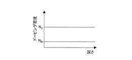
一方、基板の口径が3インチ以上の場合、基底面転位等の欠陥密度を下げ、またSiCインゴットからの基板の収率を上げる等の観点から、基板のオフ角度は従来の8°から約4°乃至それ以下が用いられている。このような小さいオフ角度を持つ基板上のエピタキシャル成長の場合、成長時に流す材料ガス中の珪素原子数に対する炭素原子数の比(C/Si比)は、従来よりも低くすることが一般的である。これは、オフ角度が小さくなるに従って表面のステップ数が減少し、ステップフロー成長が起こりにくくなって、ステップバンチングやエピタキシャル欠陥が増加しやすくなることを抑えるためである。しかし、C/Si比を低くすると、所謂サイトコンペティション(site-competition)が顕著となり、エピタキシャル成長時に、雰囲気から窒素原子のような不純物の取り込みが大きくなる。取り込まれた窒素原子はSiC中でドナーとなり、電子を供給するため、キャリア密度が上昇する。成長雰囲気中には、残留窒素が存在するため、不純物元素を添加せずに形成したノンドープ層であってもsite-competitionは生じ、C/Si比を下げて成長したノンドープ層の残留キャリア密度は、従来のC/Si比の場合よりも高くなる。この点について、図1を用いて以下で説明する。 On the other hand, when the diameter of the substrate is 3 inches or more, the off-angle of the substrate is about 4 from the conventional 8 ° from the viewpoint of decreasing the defect density such as basal plane dislocation and increasing the yield of the substrate from the SiC ingot. ° or less is used. In the case of epitaxial growth on a substrate having such a small off-angle, the ratio of the number of carbon atoms to the number of silicon atoms (C / Si ratio) in the material gas flowing during growth is generally lower than before. . This is to prevent the number of steps on the surface from decreasing as the off-angle decreases, making it difficult for step flow growth to easily increase step bunching and epitaxial defects. However, when the C / Si ratio is lowered, so-called site-competition becomes prominent, and impurities such as nitrogen atoms are taken up from the atmosphere during epitaxial growth. The incorporated nitrogen atoms become donors in SiC and supply electrons, so that the carrier density increases. Since residual nitrogen exists in the growth atmosphere, site-competition occurs even in the non-doped layer formed without adding the impurity element, and the residual carrier density of the non-doped layer grown with the C / Si ratio lowered is It becomes higher than the conventional C / Si ratio. This point will be described below with reference to FIG.
従来のようなオフ角度(8°)の基板に対して、C/Si比をXとして成長させた場合のノンドープ層の残留キャリア密度をNXとすると、約4°乃至それ以下のオフ角の基板上に成長させる場合に必要な低いC/Si比Y(通常1.0程度)で成長させた場合のノンドープ層の残留キャリア密度は、NY(通常0.8〜1×1015cm-3程度)になる。一方、デバイス動作に必要なキャリアレベルNCは、例えば1〜5×1015cm-3であって、これは、ほぼNYの程度であるため、C/Si比がYの時には、意図的にドーピングガスである窒素を導入してキャリアレベルを制御することが困難になる。さらに、厳密には、ウェーハ上の全ての部分でC/Si比が一定ではないため、局所的にC/Si比がYより小さい場合が発生し、その場合には、図1から分かるように、残留キャリア密度がNCよりも大きくなる。 When the residual carrier density of the non-doped layer when the C / Si ratio is grown as X with respect to a conventional off-angle (8 °) substrate is N X , the off-angle is about 4 ° or less. The residual carrier density of the non-doped layer when grown at the low C / Si ratio Y (usually around 1.0) required for growth on the substrate is N Y (usually around 0.8 to 1 × 10 15 cm -3 ) Become. On the other hand, the carrier level N C necessary for device operation is, for example, 1 to 5 × 10 15 cm −3 , which is about N Y , and is intentional when the C / Si ratio is Y. It is difficult to control the carrier level by introducing nitrogen, which is a doping gas. Strictly speaking, since the C / Si ratio is not constant in all parts on the wafer, there is a case where the C / Si ratio is locally smaller than Y. In this case, as can be seen from FIG. The residual carrier density becomes larger than N C.
図2aにC/Si比がYの部分でドーピングを行った場合のドーピング密度プロファイルを示し、図2bにC/Si比がYより小さい部分(0.8〜0.9程度)でドーピングを行った場合のドーピング密度プロファイルを示す。NB1とNB2がそれぞれの部分での残留キャリア密度とすると、通常NB1は0.8〜1×1015cm-3程度であり、NB2は1〜3×1015cm-3程度であるため、NB1<NB2≒NCとなる。ウェーハ内の図2aの部分において、NCが得られるようにドーピングを行ったとすると、NC−NB1がドーピング量になるため、図2bの部分では、必然的にNC−NB1+NB2がドーピング値となる。従って、NB2−NB1が図2aと図2bの部分でのドーピングばらつきとなり、これはNCの10%程度よりも大きい値となり得るため、ドーピング密度の面内分布を大きく低下させることになる。 FIG. 2a shows a doping density profile when doping is performed at the portion where the C / Si ratio is Y, and FIG. 2b shows doping when the doping is performed at the portion where the C / Si ratio is smaller than Y (about 0.8 to 0.9). A density profile is shown. When N B1 and N B2 is the residual carrier density in each part, usually N B1 is about 0.8~1 × 10 15 cm -3, N B2 is about 1~3 × 10 15 cm -3 Therefore , N B1 <N B2 ≈N C. If doping is performed so that N C can be obtained in the portion of FIG. 2 a in the wafer, N C −N B1 becomes the doping amount, and therefore, in the portion of FIG. 2 b, N C −N B1 + N B2 Is the doping value. Therefore, N B2 −N B1 becomes a doping variation in the portions of FIGS. 2 a and 2 b, which can be a value larger than about 10% of N C , thereby greatly reducing the in-plane distribution of the doping density. .
したがって、今後デバイスへの応用が期待されるSiCエピタキシャル成長基板であるが、基板のオフ角度を従来の8°から約4°乃至それ以下にすると、C/Si比を下げて成長しなければならないことに起因するドーピング密度のウェーハ面内均一性が劣化し、デバイス応用上問題であった。 Therefore, it is a SiC epitaxial growth substrate that is expected to be applied to devices in the future. However, if the off-angle of the substrate is reduced from about 8 ° to about 4 ° or less, it must be grown with a reduced C / Si ratio. The uniformity in the wafer surface of the doping density due to this deteriorated, which was a problem in device application.
ところで、本発明者等は、オフ角度が4°以下のSiC単結晶基板上に高品質のエピタキシャル膜を形成する方法として、エピタキシャル膜の材料ガス中に含まれる炭素と珪素の原子数比(C/Si)を0.5以上1.0未満にして成長させた層(欠陥低減層)と、C/Siを1.0以上1.5以下にして成長させた層(活性層)とを形成する方法を提案している(特許文献1参照)。ところが、この方法は、三角形状のエピタキシャル欠陥や表面荒れの少ないエピタキシャル膜を得ることを目的とするものであり、ウェーハ面内におけるエピタキシャル膜のドーピング密度について、均一性を担保する直接の手段を教える記載はない。 By the way, as a method of forming a high-quality epitaxial film on a SiC single crystal substrate having an off angle of 4 ° or less, the present inventors have used an atomic ratio (C) of carbon and silicon contained in the material gas of the epitaxial film. / Si) between 0.5 and 1.0 and grown (defect reduction layer) and C / Si grown between 1.0 and 1.5 (active layer) The method to do is proposed (refer patent document 1). However, this method is intended to obtain a triangular epitaxial defect and an epitaxial film with less surface roughness, and teaches a direct means for ensuring uniformity of the epitaxial film doping density in the wafer plane. There is no description.
本発明は、オフ角度が1°以上6°以下の基板を用いたエピタキシャル成長において、炭素と珪素の原子数比(C/Si)を低くした場合でも、ばらつきを抑えて、ドーピング密度のウェーハ面内均一性に優れた高品質エピタキシャル膜を有したエピタキシャルSiC単結晶基板、及びその製造方法を提供するものである。 In the present invention, even when the atomic ratio of carbon to silicon (C / Si) is lowered in epitaxial growth using a substrate with an off angle of 1 ° or more and 6 ° or less, variation is suppressed and the doping density is within the wafer surface. An epitaxial SiC single crystal substrate having a high quality epitaxial film excellent in uniformity and a method for manufacturing the same are provided.
本発明は、エピタキシャル成長時に、不純物元素を添加せずに形成したノンドープ層と、不純物元素を添加しながら形成したドープ層とをそれぞれ複数層積層し、尚且つ、そのノンドープ層及びドープ層を成長させる際のC/Si比と、それらの厚みを変えることで、上記課題を解決できることを見出し、完成したものである。 In the present invention, during epitaxial growth, a plurality of non-doped layers formed without adding an impurity element and a doped layer formed while adding an impurity element are stacked, and the non-doped layer and the doped layer are grown. The present inventors have found out that the above-mentioned problems can be solved by changing the C / Si ratio and the thickness thereof.
即ち、本発明は、
(1)オフ角度が1°以上6°以下である炭化珪素単結晶基板上に、化学気相堆積法によって形成された炭化珪素エピタキシャル膜を有するエピタキシャル炭化珪素単結晶基板であって、
該エピタキシャル膜が、不純物元素を添加しながら形成した厚さ0.5μm以下のドープ層と、不純物元素を添加せずに形成した厚さ0.1μm以下のノンドープ層とを交互に積層して、ドープ層及びノンドープ層をそれぞれ2層以上有してなり、前記ドープ層が、エピタキシャル膜の材料ガス中に含まれる炭素と珪素の原子数比(C/Si)を1.5以上2.0以下にして形成され、また、前記ノンドープ層が、エピタキシャル膜の材料ガス中に含まれる炭素と珪素の原子数比(C/Si)を0.5以上1.5未満にして形成されたことを特徴とするエピタキシャル炭化珪素単結晶基板、
(2)前記ドープ層と前記ノンドープ層をそれぞれ20回以上積層することを特徴とする上記(1)に記載のエピタキシャル炭化珪素単結晶基板、
(3)前記ドープ層の厚さが前記ノンドープ層の厚さよりも大きいことを特徴とする上記(1)又は(2)に記載のエピタキシャル炭化珪素単結晶基板、
(4)前記ドープ層のドーピング原子数密度が1×1015cm-3以上であることを特徴とする上記(1)〜(3)のいずれかに記載のエピタキシャル炭化珪素単結晶基板、
(5)オフ角度が1°以上6°以下である炭化珪素単結晶基板上に、化学気相堆積法によって炭化珪素エピタキシャル膜を形成して、エピタキシャル炭化珪素単結晶基板を製造する方法であって、
エピタキシャル膜の材料ガス中に含まれる炭素と珪素の原子数比(C/Si)を1.5以上2.0以下にして、不純物元素を添加しながら形成する厚さ0.5μm以下のドープ層と、
エピタキシャル膜の材料ガス中に含まれる炭素と珪素の原子数比(C/Si)を0.5以上1.5未満にして、不純物元素を添加せずに形成する厚さ0.1μm以下のノンドープ層と、
を交互に成長させて、ドープ層及びノンドープ層をそれぞれ2層以上有するようにして炭化珪素エピタキシャル膜を形成することを特徴とするエピタキシャル炭化珪素単結晶基板の製造方法、
である。
That is, the present invention
(1) An epitaxial silicon carbide single crystal substrate having a silicon carbide epitaxial film formed by a chemical vapor deposition method on a silicon carbide single crystal substrate having an off angle of 1 ° to 6 °,
The epitaxial film is formed by alternately laminating a doped layer having a thickness of 0.5 μm or less formed while adding an impurity element and a non-doped layer having a thickness of 0.1 μm or less formed without adding an impurity element, Each of the doped layers has two or more doped layers and non-doped layers, and the doped layer has an atomic ratio (C / Si) of carbon to silicon contained in the material gas of the epitaxial film of 1.5 to 2.0. The non-doped layer is formed with a carbon / silicon atomic ratio (C / Si) contained in the material gas of the epitaxial film of 0.5 to less than 1.5. An epitaxial silicon carbide single crystal substrate,
(2) The epitaxial silicon carbide single crystal substrate according to (1), wherein the doped layer and the non-doped layer are each laminated 20 times or more ,
(3) The epitaxial silicon carbide single crystal substrate according to (1) or (2), wherein the thickness of the doped layer is larger than the thickness of the non-doped layer,
(4) The epitaxial silicon carbide single crystal substrate according to any one of (1) to (3), wherein the doped layer has a doping atom number density of 1 × 10 15 cm −3 or more,
(5) A method of manufacturing an epitaxial silicon carbide single crystal substrate by forming a silicon carbide epitaxial film by a chemical vapor deposition method on a silicon carbide single crystal substrate having an off angle of 1 ° to 6 °. ,
Doped layer having a thickness of 0.5 μm or less formed while adding an impurity element with an atomic ratio (C / Si) of carbon to silicon contained in the material gas of the epitaxial film being 1.5 to 2.0 When,
Non-doped with a thickness of 0.1 μm or less formed without adding an impurity element by setting the atomic ratio (C / Si) of carbon and silicon contained in the material gas of the epitaxial film to 0.5 to less than 1.5 Layers,
An epitaxial silicon carbide single crystal substrate, characterized in that a silicon carbide epitaxial film is formed by alternately growing the silicon carbide epitaxial film so as to have two or more doped layers and non-doped layers,
It is.
本発明によれば、オフ角度が1°以上6°以下の基板上に形成したエピタキシャル膜において、ドーピング密度のウェーハ面内均一性に優れた、高品質なエピタキシャルSiC単結晶基板を提供することが可能である。 According to the present invention, it is possible to provide a high-quality epitaxial SiC single crystal substrate that is excellent in uniformity in the wafer surface of a doping density in an epitaxial film formed on a substrate having an off angle of 1 ° to 6 °. Is possible.
また、本発明の製造方法は、CVD法(Chemical Vapor Deposition:化学気相堆積法)を用いるため、装置構成が容易で制御性にも優れ、均一性、再現性の高いエピタキシャル膜が得られる。 In addition, since the manufacturing method of the present invention uses a CVD method (Chemical Vapor Deposition), an epitaxial film with an easy apparatus configuration and excellent controllability and high uniformity and reproducibility can be obtained.
さらに、本発明のエピタキシャルSiC単結晶基板を用いたデバイスは、ドーピング密度のウェーハ面内均一性に優れた高品質エピタキシャル膜上に形成されるため、その特性及び歩留りが向上する。 Furthermore, since the device using the epitaxial SiC single crystal substrate of the present invention is formed on a high-quality epitaxial film excellent in uniformity in the wafer surface of the doping density, its characteristics and yield are improved.
本発明の具体的な内容について述べる。
まず、SiC単結晶基板上へのエピタキシャル成長について述べる。
本発明で好適にエピタキシャル成長に用いる装置は、横型のCVD装置である。CVD法は、装置構成が簡単であり、ガスのon/offで成長を制御できるため、エピタキシャル膜の制御性、再現性に優れた成長方法である。
The specific contents of the present invention will be described.
First, epitaxial growth on a SiC single crystal substrate will be described.
The apparatus suitably used for epitaxial growth in the present invention is a horizontal CVD apparatus. The CVD method has a simple apparatus configuration and can control growth by gas on / off, and is therefore a growth method with excellent controllability and reproducibility of the epitaxial film.
図3に、従来のエピタキシャル膜成長を行う際の典型的な成長シーケンスを、ガスの導入タイミングと併せて示す。まず、成長炉に基板をセットし、成長炉内を真空排気した後、水素ガスを導入して圧力を1×10⁴〜3×10⁴Paに調整する。その後、圧力を一定に保ちながら成長炉の温度を上げ、成長温度である1550〜1650℃に達した後、材料ガスであるSiH4とC2H4およびドーピングガスであるN2を導入して成長を開始する。SiH4流量は毎分40〜50cm3、C2H4流量は毎分20〜40cm3であり、成長速度は毎時6〜7μmである。この成長速度は、通常利用されるエピタキシャル層の膜厚が10μm程度であるため、生産性を考慮して決定されたものである。一定時間成長し、所望の膜厚が得られた時点でSiH4、C2H4およびN2の導入を止め、水素ガスのみ流した状態で温度を下げる。温度が常温まで下がった後、水素ガスの導入を止め、成長室内を真空排気し、不活性ガスを成長室に導入して、成長室を大気圧に戻してから、基板を取り出す。また、この従来方式で成長を行う場合のC/Si比とN2ガス流量の変化を図4に示す。図4より、成長開始から終了までC/Si比とN2ガス流量は変化させず、一定である。 FIG. 3 shows a typical growth sequence when performing conventional epitaxial film growth together with the gas introduction timing. First, a substrate is set in a growth furnace, the inside of the growth furnace is evacuated, and then hydrogen gas is introduced to adjust the pressure to 1 × 10 4 to 3 × 10 4 Pa. Thereafter, the temperature of the growth furnace was raised while keeping the pressure constant, and after reaching the growth temperature of 1550 to 1650 ° C., the material gases SiH 4 and C 2 H 4 and the doping gas N 2 were introduced. Start growing. The SiH 4 flow rate is 40-50 cm 3 / min, the C 2 H 4 flow rate is 20-40 cm 3 / min, and the growth rate is 6-7 μm / hr. This growth rate is determined in consideration of productivity because the film thickness of the normally used epitaxial layer is about 10 μm. When the film is grown for a certain period of time and a desired film thickness is obtained, the introduction of SiH 4 , C 2 H 4 and N 2 is stopped, and the temperature is lowered with only hydrogen gas flowing. After the temperature has dropped to room temperature, the introduction of hydrogen gas is stopped, the growth chamber is evacuated, an inert gas is introduced into the growth chamber, the growth chamber is returned to atmospheric pressure, and the substrate is taken out. FIG. 4 shows changes in the C / Si ratio and N 2 gas flow rate when growth is performed by this conventional method. From FIG. 4, the C / Si ratio and the N 2 gas flow rate are not changed from the start to the end of the growth, and are constant.
次に、本発明の内容を図5の成長シーケンスで説明する。SiC単結晶基板をセットし、成長を開始するまでは、図3と同様である。成長開始直後は、SiH4とC2H4の流量比がC/Si比で1.5未満になるようにしてノンドープ層を0.1μm程度成長させる。その後SiH4とC2H4の流量比がC/Si比で1.5以上になるようにして0.2μm程度成長させるが、その時にドーピングガスである窒素を導入してドープ層とする。その後は、ノンドープ層とドープ層を繰り返し成長させて、所望の膜厚が得られた時点でSiH4、C2H4およびN2の導入を止める。その後の手順は、図3の場合と同様である。この場合のC/Si比とN2ガス流量の変化を図6に示す。このように、低いC/Si比でノンドープ層を成長させ、高いC/Si比でドープ層を成長させることにより、site-competitionが起こりにくい状態でドーピングが行えるため、制御性に優れたドーピングが可能になる。さらに、本発明では、ノンドープ層の厚さを全体的に薄くするため、前述したドーピング密度の面内不均一性も抑制される。この点について、図7を用いて、下記で一例を挙げながら説明する。 Next, the contents of the present invention will be described with reference to the growth sequence of FIG. The process is the same as in FIG. 3 until the SiC single crystal substrate is set and the growth is started. Immediately after the start of growth, the non-doped layer is grown by about 0.1 μm so that the flow ratio of SiH 4 and C 2 H 4 is less than 1.5 in terms of C / Si ratio. Thereafter, growth is carried out to about 0.2 μm so that the flow ratio of SiH 4 and C 2 H 4 is 1.5 or more in terms of C / Si ratio. At that time, nitrogen as a doping gas is introduced to form a doped layer. Thereafter, the non-doped layer and the doped layer are repeatedly grown, and the introduction of SiH 4 , C 2 H 4 and N 2 is stopped when the desired film thickness is obtained. The subsequent procedure is the same as in FIG. FIG. 6 shows changes in the C / Si ratio and the N 2 gas flow rate in this case. In this way, by growing a non-doped layer with a low C / Si ratio and growing a doped layer with a high C / Si ratio, doping can be performed in a state where site-competition hardly occurs, so doping with excellent controllability can be achieved. It becomes possible. Furthermore, in the present invention, since the thickness of the non-doped layer is reduced as a whole, the above-described in-plane non-uniformity of the doping density is also suppressed. This will be described with reference to FIG. 7 with an example.
図7aは図2aと同様の場所に、本発明を適用してドーピングした場合のドーピングプロファイルであり、理想的なドーピングプロファイルが得られた時には、ドーピング密度は点線のようになる。つまり、ドーピングガスである窒素を導入しながら形成するドープ層では、C/Si比を図1における値Yよりも高く、1.5以上にしているため、残留キャリア密度の影響を受けることなくNCが得られるようにドーピングされる。一方、ドーピングガスである窒素を導入せずに形成するノンドープ層では、C/Si比が図1における値Yである、1.0程度のため、図2aのNB1の残留キャリア密度を示すようになる。しかし実際には、ドープ層とノンドープ層の間のドーピング密度変化は連続的であるため、実線のようなプロファイルになる。そして、実効的なドーピング密度はNC1程度と考えられる。 FIG. 7a shows a doping profile when doping is performed by applying the present invention in the same place as in FIG. 2a. When an ideal doping profile is obtained, the doping density becomes a dotted line. That is, in the doped layer formed while introducing nitrogen as a doping gas, the C / Si ratio is higher than the value Y in FIG. 1 and 1.5 or more, so that N is not affected by the residual carrier density. Doped to obtain C. On the other hand, in the non-doped layer formed without introducing nitrogen as a doping gas, the C / Si ratio is about 1.0, which is the value Y in FIG. 1, so that the residual carrier density of N B1 in FIG. become. However, in practice, since the doping density change between the doped layer and the non-doped layer is continuous, the profile becomes a solid line. The effective doping density is considered to be about N C1 .
一方、図7bは図2bと同様の場所であり、図7aと同様に点線が理想的なドーピングプロファイルを示す。この場合、C/Si比が1.5以上と図1における値Yよりも高いドープ層のNCの値は残留不純物の影響を受けないため、図7aのNCと同様になるが、C/Si比が図1における値Yよりも小さい、0.8〜0.9になっているノンドープ層の残留キャリア密度は、残留不純物密度が高いため、図2bのNB2と同じになる。そして、実効的なドーピング密度はNC2程度と考えられる。従って、NC1とNC2の差が小さくなり、ドーピング密度の面内均一性が改善される。 On the other hand, FIG. 7b is the same place as FIG. 2b, and the dotted line shows an ideal doping profile as in FIG. 7a. In this case, the N C value of the doped layer having a C / Si ratio of 1.5 or higher and higher than the value Y in FIG. 1 is not affected by the residual impurities, and is similar to N C in FIG. / Si ratio is less than the value Y in FIG. 1, the residual carrier density of the undoped layer that is a 0.8 to 0.9, since the residual impurity concentration is high, the same as the N B2 of Fig 2b. The effective doping density is considered to be about N C2 . Therefore, the difference between N C1 and N C2 is reduced, and the in-plane uniformity of the doping density is improved.
本発明により、1°以上6°以下のオフ角を持った基板上のエピタキシャル膜において、ドーピングの面内均一性が高い良好なエピタキシャル膜が得られるようになるが、低いC/Si比で成長するノンドープ層は、小さいオフ角を持つ基板上の成長に必須であるため、薄すぎるとエピタキシャル欠陥等が生じ膜質が劣化する。また、厚すぎると全体のドーピング密度の面内均一性に悪影響を与えるとともに、基板に垂直に電流を流す現状のデバイスにおいては抵抗が高くなるという問題が発生する。一方、高いC/Si比で成長するドープ層は、ノンドープ層より薄いとドーピング密度の面内均一性の向上に対する寄与が小さく、厚すぎると膜質の劣化につながる。 According to the present invention, in an epitaxial film on a substrate having an off angle of 1 ° or more and 6 ° or less, a good epitaxial film with high in-plane doping uniformity can be obtained, but it is grown with a low C / Si ratio. Since the non-doped layer is essential for growth on a substrate having a small off angle, if it is too thin, an epitaxial defect or the like occurs and the film quality deteriorates. On the other hand, if the thickness is too large, the in-plane uniformity of the entire doping density is adversely affected, and the current device in which current flows perpendicularly to the substrate has a problem of increased resistance. On the other hand, if the doped layer grown at a high C / Si ratio is thinner than the non-doped layer, the contribution to the improvement of in-plane uniformity of the doping density is small, and if it is too thick, the film quality is deteriorated.
以上の状況を考慮し、発明者らが検討した結果、ノンドープ層の厚さは0.1μm以下、より好適には0.05〜0.1μmであり、ドープ層の厚さは0.5μm以下、より好適には0.2〜0.5μmである。さらに、ドープ層及びノンドープ層は、それぞれ2層以上有するようにするが、ノンドープ層とドープ層の積層回数は、多い方がエピタキシャル膜全体でのドーピング密度の平均化が進み、面内均一性の向上に効果的であるため、実際に必要とされるエピタキシャル膜全体の厚さも考慮すると、ノンドープ層とドープ層の積層回数は、それぞれが20回程度より多いことが好適である。ノンドープ層とドープ層の積層順番に関しては、SiC基板上に成長を開始する時は、小さいオフ角を持つ基板上の成長になるため、低いC/Si比、すなわちノンドープ層が必要である。一方、最表面は、デバイスの電極と接触する部分であるため、ドープ層が必要である。 As a result of examination by the inventors in view of the above situation, the thickness of the non-doped layer is 0.1 μm or less, more preferably 0.05 to 0.1 μm, and the thickness of the doped layer is 0.5 μm or less. More preferably, the thickness is 0.2 to 0.5 μm. Furthermore, each of the doped layer and the non-doped layer is made to have two or more layers. However, the more the number of laminations of the non-doped layer and the doped layer, the more the doping density is averaged over the entire epitaxial film, and the in-plane uniformity is more Considering the thickness of the entire epitaxial film that is actually required, it is preferable that the number of laminations of the non-doped layer and the doped layer is more than about 20 each because it is effective for improvement. Regarding the stacking order of the non-doped layer and the doped layer, a low C / Si ratio, that is, a non-doped layer is required when starting growth on a SiC substrate because growth is performed on a substrate having a small off angle. On the other hand, since the outermost surface is a part that contacts the electrode of the device, a doped layer is necessary.
また、ノンドープ層を成長する時のC/Si比は、低オフ角基板上の成長を考慮すると0.5以上1.5未満であることが必要である。0.5未満では、過剰なSi原子が基板表面に凝縮するSiドロップレットと呼ばれる欠陥が形成され易く、1.5以上になると表面荒れやエピタキシャル欠陥が増加する。より好適には0.8〜1.2である。一方、ドープ層を成長する時のC/Si比は、低すぎるとsite-competitionの影響が現れ、高すぎると三角形欠陥等のエピタキシャル欠陥が増加するため、1.5以上2.0以下、より好適には1.5〜1.8である。さらに、ドープ層のドーピング原子数密度は、図7a、図7bより、NB1およびNB2より大きい事が必要であって、そのためには1×1015cm-3以上が必要であるが、ドーピング原子数密度が高すぎると表面荒れが生じるため、より好適には1×1015cm-3以上1×1017cm-3以下である。 In addition, the C / Si ratio when growing the non-doped layer needs to be 0.5 or more and less than 1.5 in consideration of the growth on the low off-angle substrate. If it is less than 0.5, defects called Si droplets in which excessive Si atoms condense on the substrate surface are likely to be formed, and if it is 1.5 or more, surface roughness and epitaxial defects increase. More preferably, it is 0.8 to 1.2. On the other hand, if the C / Si ratio when growing the doped layer is too low, the effect of site-competition appears, and if it is too high, epitaxial defects such as triangular defects increase. Preferably it is 1.5-1.8. Furthermore, the doping atom number density of the doped layer needs to be larger than N B1 and N B2 from FIGS. 7a and 7b, and for this purpose, it is necessary to be 1 × 10 15 cm −3 or more. When the atomic number density is too high, surface roughness occurs, and therefore, it is more preferably 1 × 10 15 cm −3 or more and 1 × 10 17 cm −3 or less.
エピタキシャル膜全体の厚さについては、通常形成されるデバイスの耐圧、エピタキシャル膜の生産性等を考慮した場合、5μm以上50μm以下が好ましい。また、基板のオフ角が1°以上6°以下であるのは、1°未満であるとオフ角が小さすぎて、本発明の効果を十分に発揮することができず、6°を超えると、C/Si比が高い状態で成長でき、本発明を用いなくても面内均一性を上げられるからである。 The total thickness of the epitaxial film is preferably 5 μm or more and 50 μm or less in consideration of the breakdown voltage of a device that is normally formed, the productivity of the epitaxial film, and the like. Further, the off angle of the substrate is not less than 1 ° and not more than 6 °. If the angle is less than 1 °, the off angle is too small to fully exhibit the effects of the present invention. This is because the film can be grown with a high C / Si ratio and the in-plane uniformity can be improved without using the present invention.
そして、本発明によれば、SiC単結晶基板にエピタキシャル膜を成長する際に、ノンドープ層とドープ層をそれぞれ複数層積層し、そのノンドープ層とドープ層を成長する時のC/Si比および厚さを変えることで、ドーピング密度の面内均一性をσ/meanで5%以下にすることができる。ただしこの場合は、図7から分かるように、ノンドープ層とドープ層との積層部分のドーピング密度の平均値を、通常の容量−電圧測定から得られるドーピングプロファイルで求めることはできないため、エピタキシャル膜の表面と基板裏面にオーミック電極を形成し、電極間の電流値をドーピング密度と等価とみなし、その面内均一性で評価する。 According to the present invention, when an epitaxial film is grown on a SiC single crystal substrate, a plurality of non-doped layers and doped layers are stacked, and the C / Si ratio and thickness when growing the non-doped layers and doped layers are increased. By changing the thickness, the in-plane uniformity of the doping density can be reduced to 5% or less in terms of σ / mean. However, in this case, as can be seen from FIG. 7, the average value of the doping density of the laminated portion of the non-doped layer and the doped layer cannot be obtained by the doping profile obtained from the normal capacitance-voltage measurement. Ohmic electrodes are formed on the front surface and the back surface of the substrate, and the current value between the electrodes is regarded as equivalent to the doping density, and the in-plane uniformity is evaluated.
本発明においてエピタキシャル膜を形成する際に添加する不純物元素は、主に窒素を例に説明したが、窒素以外にも、例えばアルミニウム等を用いてドープ層を形成するようにしてもよい。また、エピタキシャル膜の材料ガスについては、SiH4とC2H4を例に説明したが、これら以外の珪素源や炭素源を用いてもよいことは勿論である。 In the present invention, the impurity element added when forming the epitaxial film has been described mainly using nitrogen as an example. However, other than nitrogen, for example, aluminum or the like may be used to form a doped layer. In addition, as the material gas for the epitaxial film, SiH 4 and C 2 H 4 have been described as examples, but it is needless to say that other silicon sources or carbon sources may be used.
このようにして成長されたエピタキシャル膜を有する本発明の基板上に好適に形成されるデバイスの例としては、ショットキーバリアダイオード、PINダイオード、MOSダイオード、MOSトランジスタ等が挙げられ、特に電力制御用に用いられるデバイスが好適な例である。 Examples of devices suitably formed on the substrate of the present invention having the epitaxial film thus grown include Schottky barrier diodes, PIN diodes, MOS diodes, MOS transistors, etc., particularly for power control. The device used for is a suitable example.
(実施例1)
3インチ(76mm)ウェーハ用SiC単結晶インゴットから、約400μmの厚さでスライスし、粗削りとダイヤモンド砥粒による通常研磨を実施して、4H型のポリタイプを有するSiC単結晶基板を用意した。この基板のSi面に、エピタキシャル成長を実施した。基板のオフ角は4°である。成長の手順としては、成長炉に基板をセットし、成長炉内を真空排気した後、水素ガスを毎分150L導入しながら圧力を1.0×10⁴Paに調整した。その後、圧力を一定に保ちながら成長炉の温度を1600℃まで上げ、SiH4流量を毎分40cm3、C2H4流量を毎分22cm3(C/Si比1.1)にしてノンドープ層の成長を開始した。ノンドープ層を0.1μm成長させた後、SiH4流量を毎分40cm3、C2H4流量を毎分30cm3(C/Si比1.5)にし、さらにドーピングガスであるN2流量を毎分30cm3にして(ドーピング原子数密度1×1016 cm-3)、ドープ層を0.2μm成長させた。その後、N2の導入を止め、再びノンドープ層を0.1μm成長させて、更に、N2流量を毎分30cm3にしてドープ層を0.2μm成長させて、以降このようにして、ノンドープ層とドープ層をそれぞれ合計30回成長させ、最上層がドープ層となるようにした。
Example 1
A SiC single crystal substrate having a 4H type polytype was prepared by slicing from a SiC single crystal ingot for a 3-inch (76 mm) wafer to a thickness of about 400 μm, roughing and normal polishing with diamond abrasive grains. Epitaxial growth was performed on the Si surface of the substrate. The off angle of the substrate is 4 °. As a growth procedure, a substrate was set in a growth furnace, the inside of the growth furnace was evacuated, and then the pressure was adjusted to 1.0 × 10 4 Pa while introducing 150 L of hydrogen gas per minute. Thereafter, the temperature of the growth furnace is raised to 1600 ° C. while keeping the pressure constant, and the SiH 4 flow rate is 40 cm 3 / min and the C 2 H 4 flow rate is 22 cm 3 / min (C / Si ratio 1.1). Started. After growing the non-doped layer by 0.1 μm, the flow rate of SiH 4 is 40 cm 3 / min, the flow rate of C 2 H 4 is 30 cm 3 / min (C / Si ratio 1.5), and the flow rate of N 2 as a doping gas is changed per minute The doped layer was grown to 0.2 μm with 30 cm 3 (doping
このようにしてエピタキシャル成長を行った膜の光学顕微鏡写真を図8に示す。図8より、表面荒れや欠陥の少ない良好な膜が得られていることが分かる。このエピタキシャル膜のドーピング密度を電流値により評価した結果を図9に示す。均一性は良好であり、σ/meanで表した面内均一性は4.5%であった。 An optical micrograph of the film epitaxially grown in this way is shown in FIG. FIG. 8 shows that a good film with less surface roughness and defects is obtained. FIG. 9 shows the result of evaluating the doping density of this epitaxial film based on the current value. The uniformity was good, and the in-plane uniformity represented by σ / mean was 4.5%.
(実施例2)
実施例1と同様にスライス、粗削り、通常研磨を行った、4H型のポリタイプを有する3インチ(76mm)のSiC単結晶基板のSi面に、エピタキシャル成長を実施した。基板のオフ角は4°である。成長開始までの手順、温度等は、実施例1と同様であり、SiH4流量を毎分40cm3、C2H4流量を毎分22cm3(C/Si比1.1)にしてノンドープ層の成長を開始した。ノンドープ層を0.05μm成長させた後、SiH4流量を毎分40cm3、C2H4流量を毎分30cm3(C/Si比1.5)にし、さらにドーピングガスであるN2流量を毎分3cm3にして(ドーピング原子数密度1×1015 cm-3)、ドープ層を0.5μm成長させた。その後、N2の導入を止め、再びノンドープ層を0.05μm成長させて、更に、N2流量を毎分3cm3にしてドープ層を0.5μm成長させて、以降このようにして、ノンドープ層とドープ層をそれぞれ合計20回成長させた。このようにしてエピタキシャル成長を行った膜は、表面荒れや欠陥の少ない良好な膜であり、電流値で評価した面内均一性のσ/meanは3.5%であった。
(Example 2)
Epitaxial growth was carried out on the Si surface of a 3 inch (76 mm) SiC single crystal substrate having a 4H type polytype, which was sliced, roughly ground, and normally polished as in Example 1. The off angle of the substrate is 4 °. The procedure up to the start of growth, the temperature, etc. are the same as in Example 1, and the growth of the non-doped layer is performed by setting the SiH 4 flow rate to 40 cm 3 / min and the C 2 H 4 flow rate to 22 cm 3 / C (Si ratio 1.1). Started. After growing the non-doped layer by 0.05 μm, the flow rate of SiH 4 is 40 cm 3 / min, the flow rate of C 2 H 4 is 30 cm 3 / min (C / Si ratio 1.5), and the flow rate of N 2 as a doping gas is changed per minute in the 3 cm 3 (the number of
(実施例3)
実施例1と同様にスライス、粗削り、通常研磨を行った、4H型のポリタイプを有する3インチ(76mm)のSiC単結晶基板のSi面に、エピタキシャル成長を実施した。基板のオフ角は4°である。成長開始までの手順、温度等は、実施例1と同様であり、SiH4流量を毎分40cm3、C2H4流量を毎分10cm3(C/Si比0.5)にしてノンドープ層の成長を開始した。ノンドープ層を0.1μm成長させた後、SiH4流量を毎分40cm3、C2H4流量を毎分40cm3(C/Si比2.0)にし、さらにドーピングガスであるN2流量を毎分30cm3(ドーピング原子数密度1×1016 cm-3)にしてドープ層を0.2μm成長させた。その後、N2の導入を止め、再びノンドープ層を0.1μm成長させて、更に、N2流量を毎分30cm3にしてドープ層を0.2μm成長させて、以降このようにして、ノンドープ層とドープ層をそれぞれ合計30回成長させた。このようにしてエピタキシャル成長を行った膜は、表面荒れや欠陥の少ない良好な膜であり、電流値で評価した面内均一性のσ/meanは4.7%であった。
(Example 3)
Epitaxial growth was carried out on the Si surface of a 3 inch (76 mm) SiC single crystal substrate having a 4H type polytype, which was sliced, roughly ground, and normally polished as in Example 1. The off angle of the substrate is 4 °. The procedure up to the start of growth, the temperature, etc. are the same as in Example 1, and the growth of the non-doped layer is performed by setting the SiH 4 flow rate to 40 cm 3 / min and the C 2 H 4 flow rate to 10 cm 3 / min (C / Si ratio 0.5). Started. After the non-doped layer was 0.1μm grown, the SiH 4 min flow rate 40cm 3, C 2 H 4 per minute flow rate 40cm 3 (C / Si ratio 2.0), per minute N 2 flow rate is more doping gas The doped layer was grown to 0.2 μm at 30 cm 3 (doping
(実施例4)
実施例1と同様にスライス、粗削り、通常研磨を行った、4H型のポリタイプを有する3インチ(76mm)のSiC単結晶基板のSi面に、エピタキシャル成長を実施した。基板のオフ角は4°である。成長開始までの手順、温度等は、実施例1と同様であり、SiH4流量を毎分40cm3、C2H4流量を毎分10cm3(C/Si比0.5)にしてノンドープ層の成長を開始した。ノンドープ層を0.05μm成長させた後、SiH4流量を毎分40cm3、C2H4流量を毎分40cm3(C/Si比2.0)にし、さらにドーピングガスであるN2流量を毎分300cm3(ドーピング原子数密度1×1017 cm-3)にして、ドープ層を0.5μm成長させた。その後、N2の導入を止め、再びノンドープ層を0.05μm成長させて、更に、N2流量を毎分300cm3にしてドープ層を0.5μm成長させて、以降このようにして、ノンドープ層とドープ層をそれぞれ合計20回成長させた。このようにしてエピタキシャル成長を行った膜は、表面荒れや欠陥の少ない良好な膜であり、電流値で評価した面内均一性のσ/meanは4.0%であった。
Example 4
Epitaxial growth was carried out on the Si surface of a 3 inch (76 mm) SiC single crystal substrate having a 4H type polytype, which was sliced, roughly ground, and normally polished as in Example 1. The off angle of the substrate is 4 °. The procedure up to the start of growth, the temperature, etc. are the same as in Example 1, and the growth of the non-doped layer is performed by setting the SiH 4 flow rate to 40 cm 3 / min and the C 2 H 4 flow rate to 10 cm 3 / min (C / Si ratio 0.5). Started. After the non-doped layer is 0.05μm grown, the SiH 4 min flow rate 40cm 3, C 2 H 4 per minute flow rate 40cm 3 (C / Si ratio 2.0), per minute N 2 flow rate is more doping gas The doped layer was grown to 0.5 μm at 300 cm 3 (doping
(実施例5)
実施例1と同様にスライス、粗削り、通常研磨を行った、4H型のポリタイプを有する3インチ(76mm)のSiC単結晶基板のSi面に、エピタキシャル成長を実施した。基板のオフ角は1°である。成長開始までの手順、温度等は、実施例1と同様であり、SiH4流量を毎分40cm3、C2H4流量を毎分10cm3(C/Si比0.5)にしてノンドープ層の成長を開始した。ノンドープ層を0.1μm成長させた後、SiH4流量を毎分40cm3、C2H4流量を毎分30cm3(C/Si比1.5)にし、さらにドーピングガスであるN2流量を毎分30cm3(ドーピング原子数密度1×1016 cm-3)にして、ドープ層を0.2μm成長させた。その後、N2の導入を止め、再びノンドープ層を0.1μm成長させて、更に、N2流量を毎分30cm3にしてドープ層を0.2μm成長させて、以降このようにして、ノンドープ層とドープ層をそれぞれ合計30回成長させた。このようにしてエピタキシャル成長を行った膜は、表面荒れや欠陥の少ない良好な膜であり、電流値で評価した面内均一性のσ/meanは4.8%であった。
(Example 5)
Epitaxial growth was carried out on the Si surface of a 3 inch (76 mm) SiC single crystal substrate having a 4H type polytype, which was sliced, roughly ground, and normally polished as in Example 1. The off angle of the substrate is 1 °. The procedure up to the start of growth, the temperature, etc. are the same as in Example 1, and the growth of the non-doped layer is performed by setting the SiH 4 flow rate to 40 cm 3 / min and the C 2 H 4 flow rate to 10 cm 3 / min (C / Si ratio 0.5). Started. After growing the non-doped layer by 0.1 μm, the flow rate of SiH 4 is 40 cm 3 / min, the flow rate of C 2 H 4 is 30 cm 3 / min (C / Si ratio 1.5), and the flow rate of N 2 as a doping gas is changed per minute The doped layer was grown to 0.2 μm at 30 cm 3 (doping
(実施例6)
実施例1と同様にスライス、粗削り、通常研磨を行った、4H型のポリタイプを有する3インチ(76mm)のSiC単結晶基板のSi面に、エピタキシャル成長を実施した。基板のオフ角は6°である。成長開始までの手順、温度等は、実施例1と同様であり、SiH4流量を毎分40cm3、C2H4流量を毎分22cm3(C/Si比1.1)にしてノンドープ層の成長を開始した。ノンドープ層を0.1μm成長させた後、SiH4流量を毎分40cm3、C2H4流量を毎分30cm3(C/Si比1.5)にし、さらにドーピングガスであるN2流量を毎分30cm3(ドーピング原子数密度1×1016 cm-3)にして、ドープ層を0.2μm成長させた。その後、N2の導入を止め、再びノンドープ層を0.1μm成長させて、更に、N2流量を毎分30cm3にしてドープ層を0.2μm成長させて、以降このようにして、ノンドープ層とドープ層をそれぞれ合計30回成長させた。このようにしてエピタキシャル成長を行った膜は、表面荒れや欠陥の少ない良好な膜であり、電流値で評価した面内均一性のσ/meanは4.2%であった。
(Example 6)
Epitaxial growth was carried out on the Si surface of a 3 inch (76 mm) SiC single crystal substrate having a 4H type polytype, which was sliced, roughly ground, and normally polished as in Example 1. The off angle of the substrate is 6 °. The procedure up to the start of growth, the temperature, etc. are the same as in Example 1, and the growth of the non-doped layer is performed by setting the SiH 4 flow rate to 40 cm 3 / min and the C 2 H 4 flow rate to 22 cm 3 / C (Si ratio 1.1). Started. After growing the non-doped layer by 0.1 μm, the flow rate of SiH 4 is 40 cm 3 / min, the flow rate of C 2 H 4 is 30 cm 3 / min (C / Si ratio 1.5), and the flow rate of N 2 as a doping gas is changed per minute The doped layer was grown to 0.2 μm at 30 cm 3 (doping
(比較例1)
比較例として、実施例1と同様にスライス、粗削り、通常研磨を行った、4H型のポリタイプを有する3インチ(76mm)のSiC単結晶基板のSi面に、エピタキシャル成長を実施した。基板のオフ角は4°である。成長開始までの手順、温度等は、実施例1と同様であるが、成長は、SiH4流量を毎分40cm3、C2H4流量を毎分22cm3(C/Si比1.1)にし、さらにドーピングガスであるN2流量を1cm3(ドーピング原子数密度1×1016 cm-3)にして、ドープ層を10μm成長した。このようにしてエピタキシャル成長を行った膜は、表面荒れや欠陥の少ない良好な膜であるが、電流値で評価した面内均一性のσ/meanは15%であった。
(Comparative Example 1)
As a comparative example, epitaxial growth was performed on the Si surface of a 3 inch (76 mm) SiC single crystal substrate having a 4H type polytype, which was sliced, roughly cut, and normally polished as in Example 1. The off angle of the substrate is 4 °. The procedure up to the start of growth, temperature, and the like are the same as in Example 1. However, the growth is performed by setting the SiH 4 flow rate to 40 cm 3 / min, the C 2 H 4 flow rate to 22 cm 3 / min (C / Si ratio 1.1), Further, the N 2 flow rate as a doping gas was set to 1 cm 3 (doping
この発明によれば、SiC単結晶基板上へのエピタキシャル成長において、ドーピング密度の面内均一性に優れた高品質エピタキシャル膜を有するエピタキシャルSiC単結晶基板を作成することが可能である。そのため、このような基板上に電子デバイスを形成すればデバイスの特性及び歩留まりが向上することが期待できる。本実施例においては、材料ガスとしてSiH4及びC2H4を用いているが、Si源としてトリクロルシランを用い、C源としてC3H8等を用いた場合についても同様である。 According to the present invention, it is possible to produce an epitaxial SiC single crystal substrate having a high quality epitaxial film excellent in in-plane uniformity of doping density in epitaxial growth on the SiC single crystal substrate. Therefore, if an electronic device is formed on such a substrate, it can be expected that the characteristics and yield of the device are improved. In this embodiment, SiH 4 and C 2 H 4 are used as the material gas, but the same applies to the case where trichlorosilane is used as the Si source and C 3 H 8 is used as the C source.
Claims (5)
該エピタキシャル膜が、不純物元素を添加しながら形成した厚さ0.5μm以下のドープ層と、不純物元素を添加せずに形成した厚さ0.1μm以下のノンドープ層とを交互に積層して、ドープ層及びノンドープ層をそれぞれ2層以上有してなり、前記ドープ層が、エピタキシャル膜の材料ガス中に含まれる炭素と珪素の原子数比(C/Si)を1.5以上2.0以下にして形成され、また、前記ノンドープ層が、エピタキシャル膜の材料ガス中に含まれる炭素と珪素の原子数比(C/Si)を0.5以上1.5未満にして形成されたことを特徴とするエピタキシャル炭化珪素単結晶基板。 An epitaxial silicon carbide single crystal substrate having a silicon carbide epitaxial film formed by a chemical vapor deposition method on a silicon carbide single crystal substrate having an off angle of 1 ° to 6 °,
The epitaxial film is formed by alternately laminating a doped layer having a thickness of 0.5 μm or less formed while adding an impurity element and a non-doped layer having a thickness of 0.1 μm or less formed without adding an impurity element, Each of the doped layers has two or more doped layers and non-doped layers, and the doped layer has an atomic ratio (C / Si) of carbon to silicon contained in the material gas of the epitaxial film of 1.5 to 2.0. The non-doped layer is formed with a carbon / silicon atomic ratio (C / Si) contained in the material gas of the epitaxial film of 0.5 to less than 1.5. An epitaxial silicon carbide single crystal substrate.
エピタキシャル膜の材料ガス中に含まれる炭素と珪素の原子数比(C/Si)を1.5以上2.0以下にして、不純物元素を添加しながら形成する厚さ0.5μm以下のドープ層と、
エピタキシャル膜の材料ガス中に含まれる炭素と珪素の原子数比(C/Si)を0.5以上1.5未満にして、不純物元素を添加せずに形成する厚さ0.1μm以下のノンドープ層と、
を交互に成長させて、ドープ層及びノンドープ層をそれぞれ2層以上有するようにして炭化珪素エピタキシャル膜を形成することを特徴とするエピタキシャル炭化珪素単結晶基板の製造方法。 A method for producing an epitaxial silicon carbide single crystal substrate by forming a silicon carbide epitaxial film by a chemical vapor deposition method on a silicon carbide single crystal substrate having an off angle of 1 ° to 6 °,
Doped layer having a thickness of 0.5 μm or less formed while adding an impurity element with an atomic ratio (C / Si) of carbon to silicon contained in the material gas of the epitaxial film being 1.5 to 2.0 When,
Non-doped with a thickness of 0.1 μm or less formed without adding an impurity element by setting the atomic ratio (C / Si) of carbon and silicon contained in the material gas of the epitaxial film to 0.5 to less than 1.5 Layers,
A method of manufacturing an epitaxial silicon carbide single crystal substrate, wherein a silicon carbide epitaxial film is formed by alternately growing and forming a silicon carbide epitaxial film so as to have two or more doped layers and non-doped layers.
Priority Applications (6)
| Application Number | Priority Date | Filing Date | Title |
|---|---|---|---|
| JP2010109105A JP4880052B2 (en) | 2010-05-11 | 2010-05-11 | Epitaxial silicon carbide single crystal substrate and manufacturing method thereof |
| CN201180018417.5A CN102844474B (en) | 2010-05-11 | 2011-05-10 | Epitaxial silicon carbide single crystal substrate and manufacture method thereof |
| KR1020127025335A KR101430217B1 (en) | 2010-05-11 | 2011-05-10 | Epitaxial silicon carbide single-crystal substrate and method for producing the same |
| EP11780725.5A EP2570522B1 (en) | 2010-05-11 | 2011-05-10 | Epitaxial silicon carbide single-crystal substrate and method for producing the same |
| US13/697,211 US8901570B2 (en) | 2010-05-11 | 2011-05-10 | Epitaxial silicon carbide single crystal substrate and process for producing the same |
| PCT/JP2011/061124 WO2011142470A1 (en) | 2010-05-11 | 2011-05-10 | Epitaxial silicon carbide single-crystal substrate and method for producing the same |
Applications Claiming Priority (1)
| Application Number | Priority Date | Filing Date | Title |
|---|---|---|---|
| JP2010109105A JP4880052B2 (en) | 2010-05-11 | 2010-05-11 | Epitaxial silicon carbide single crystal substrate and manufacturing method thereof |
Publications (2)
| Publication Number | Publication Date |
|---|---|
| JP2011236085A JP2011236085A (en) | 2011-11-24 |
| JP4880052B2 true JP4880052B2 (en) | 2012-02-22 |
Family
ID=44914519
Family Applications (1)
| Application Number | Title | Priority Date | Filing Date |
|---|---|---|---|
| JP2010109105A Active JP4880052B2 (en) | 2010-05-11 | 2010-05-11 | Epitaxial silicon carbide single crystal substrate and manufacturing method thereof |
Country Status (6)
| Country | Link |
|---|---|
| US (1) | US8901570B2 (en) |
| EP (1) | EP2570522B1 (en) |
| JP (1) | JP4880052B2 (en) |
| KR (1) | KR101430217B1 (en) |
| CN (1) | CN102844474B (en) |
| WO (1) | WO2011142470A1 (en) |
Families Citing this family (30)
| Publication number | Priority date | Publication date | Assignee | Title |
|---|---|---|---|---|
| KR101926694B1 (en) * | 2012-05-30 | 2018-12-07 | 엘지이노텍 주식회사 | Silicon carbide epi wafer and method of fabricating the same |
| KR101926678B1 (en) * | 2012-05-31 | 2018-12-11 | 엘지이노텍 주식회사 | Silicon carbide epi wafer and method of fabricating the same |
| US8860040B2 (en) | 2012-09-11 | 2014-10-14 | Dow Corning Corporation | High voltage power semiconductor devices on SiC |
| US9018639B2 (en) | 2012-10-26 | 2015-04-28 | Dow Corning Corporation | Flat SiC semiconductor substrate |
| TW201417149A (en) * | 2012-10-31 | 2014-05-01 | Lg Innotek Co Ltd | Epitaxial wafer |
| US9797064B2 (en) | 2013-02-05 | 2017-10-24 | Dow Corning Corporation | Method for growing a SiC crystal by vapor deposition onto a seed crystal provided on a support shelf which permits thermal expansion |
| US9017804B2 (en) | 2013-02-05 | 2015-04-28 | Dow Corning Corporation | Method to reduce dislocations in SiC crystal growth |
| US9738991B2 (en) | 2013-02-05 | 2017-08-22 | Dow Corning Corporation | Method for growing a SiC crystal by vapor deposition onto a seed crystal provided on a supporting shelf which permits thermal expansion |
| US8940614B2 (en) | 2013-03-15 | 2015-01-27 | Dow Corning Corporation | SiC substrate with SiC epitaxial film |
| US20170170279A1 (en) * | 2014-02-27 | 2017-06-15 | Kyocera Corporation | Silicon carbide crystal ingot, silicon carbide wafer, and method for producing silicon carbide crystal ingot and silicon carbide wafer |
| JP6289952B2 (en) | 2014-03-19 | 2018-03-07 | 株式会社東芝 | SiC epitaxial substrate manufacturing method, semiconductor device manufacturing method |
| JP6306411B2 (en) * | 2014-04-17 | 2018-04-04 | 株式会社日立国際電気 | Semiconductor device manufacturing method, substrate processing apparatus, and program |
| WO2015170500A1 (en) * | 2014-05-08 | 2015-11-12 | 三菱電機株式会社 | Sic epitaxial wafer and method for manufacturing silicon carbide semiconductor device |
| US9279192B2 (en) | 2014-07-29 | 2016-03-08 | Dow Corning Corporation | Method for manufacturing SiC wafer fit for integration with power device manufacturing technology |
| KR102203025B1 (en) * | 2014-08-06 | 2021-01-14 | 엘지이노텍 주식회사 | Method of fabricating silicone carbide epi wafer |
| CN111799324A (en) * | 2015-05-18 | 2020-10-20 | 住友电气工业株式会社 | Silicon carbide epitaxial substrate, silicon carbide semiconductor device, and method for manufacturing silicon carbide semiconductor device |
| WO2017043165A1 (en) * | 2015-09-11 | 2017-03-16 | 住友電気工業株式会社 | Silicon carbide epitaxial substrate, and method for manufacturing silicon carbide semiconductor device |
| JP6584253B2 (en) * | 2015-09-16 | 2019-10-02 | ローム株式会社 | SiC epitaxial wafer, SiC epitaxial wafer manufacturing apparatus, SiC epitaxial wafer manufacturing method, and semiconductor device |
| DE112016004600T5 (en) * | 2015-10-07 | 2018-06-21 | Sumitomo Electric Industries, Ltd. | Epitaxial silicon carbide substrate and method of manufacturing a silicon carbide semiconductor device |
| US9679763B1 (en) | 2015-11-20 | 2017-06-13 | International Business Machines Corporation | Silicon-on-insulator fin field-effect transistor device formed on a bulk substrate |
| JP6351874B2 (en) | 2015-12-02 | 2018-07-04 | 三菱電機株式会社 | Silicon carbide epitaxial substrate and silicon carbide semiconductor device |
| US9537011B1 (en) | 2015-12-14 | 2017-01-03 | International Business Machines Corporation | Partially dielectric isolated fin-shaped field effect transistor (FinFET) |
| US11430882B2 (en) | 2016-06-24 | 2022-08-30 | Wolfspeed, Inc. | Gallium nitride high-electron mobility transistors with p-type layers and process for making the same |
| US10892356B2 (en) | 2016-06-24 | 2021-01-12 | Cree, Inc. | Group III-nitride high-electron mobility transistors with buried p-type layers and process for making the same |
| US10840334B2 (en) | 2016-06-24 | 2020-11-17 | Cree, Inc. | Gallium nitride high-electron mobility transistors with deep implanted p-type layers in silicon carbide substrates for power switching and radio frequency applications and process for making the same |
| US10192980B2 (en) * | 2016-06-24 | 2019-01-29 | Cree, Inc. | Gallium nitride high-electron mobility transistors with deep implanted p-type layers in silicon carbide substrates for power switching and radio frequency applications and process for making the same |
| CN107068539B (en) * | 2016-12-15 | 2019-11-22 | 中国电子科技集团公司第五十五研究所 | The method for reducing silicon carbide epitaxy base plane dislocation density |
| JP6748572B2 (en) * | 2016-12-28 | 2020-09-02 | 昭和電工株式会社 | P-type SiC epitaxial wafer and manufacturing method thereof |
| US11929428B2 (en) | 2021-05-17 | 2024-03-12 | Wolfspeed, Inc. | Circuits and group III-nitride high-electron mobility transistors with buried p-type layers improving overload recovery and process for implementing the same |
| CN117448955B (en) * | 2023-12-21 | 2024-03-29 | 南京百识电子科技有限公司 | Preparation method of silicon carbide epitaxial structure |
Family Cites Families (15)
| Publication number | Priority date | Publication date | Assignee | Title |
|---|---|---|---|---|
| CA2269912A1 (en) * | 1997-08-27 | 1999-03-04 | Makoto Kitabatake | Silicon carbide substrate, process for producing the same, and semiconductor element containing silicon carbide substrate |
| US6306211B1 (en) | 1999-03-23 | 2001-10-23 | Matsushita Electric Industrial Co., Ltd. | Method for growing semiconductor film and method for fabricating semiconductor device |
| JP2003264154A (en) * | 1999-03-23 | 2003-09-19 | Matsushita Electric Ind Co Ltd | Method of growing semiconductor film and method for manufacturing semiconductor device |
| JP3443379B2 (en) * | 1999-03-23 | 2003-09-02 | 松下電器産業株式会社 | Method for growing semiconductor film and method for manufacturing semiconductor device |
| JP3811624B2 (en) * | 2001-04-27 | 2006-08-23 | 松下電器産業株式会社 | Semiconductor device |
| EP1306890A2 (en) * | 2001-10-25 | 2003-05-02 | Matsushita Electric Industrial Co., Ltd. | Semiconductor substrate and device comprising SiC and method for fabricating the same |
| JP2003234301A (en) * | 2001-10-25 | 2003-08-22 | Matsushita Electric Ind Co Ltd | Semiconductor substrate, semiconductor element and method for manufacturing the same |
| TW200307064A (en) * | 2002-03-19 | 2003-12-01 | Central Res Inst Elect | Method for preparing SiC crystal with reduced micro-pipes extended from substrate, SiC crystal, SiC monocrystalline film, SiC semiconductor component, SiC monocrystalline substrate and electronic device, and method for producing large SiC crystal |
| US7199442B2 (en) * | 2004-07-15 | 2007-04-03 | Fairchild Semiconductor Corporation | Schottky diode structure to reduce capacitance and switching losses and method of making same |
| EP1619276B1 (en) * | 2004-07-19 | 2017-01-11 | Norstel AB | Homoepitaxial growth of SiC on low off-axis SiC wafers |
| JP2007182330A (en) * | 2004-08-24 | 2007-07-19 | Bridgestone Corp | Silicon carbide monocrystal wafer and its manufacturing method |
| US7391058B2 (en) * | 2005-06-27 | 2008-06-24 | General Electric Company | Semiconductor devices and methods of making same |
| WO2009048997A1 (en) * | 2007-10-12 | 2009-04-16 | The Government Of The United States Of America, As Represented By The Secretary Of The Navy | Producing epitaxial layers with low basal plane dislocation concentrations |
| JP4987792B2 (en) * | 2008-04-17 | 2012-07-25 | 新日本製鐵株式会社 | Epitaxial silicon carbide single crystal substrate manufacturing method |
| JP5458509B2 (en) * | 2008-06-04 | 2014-04-02 | 日立金属株式会社 | Silicon carbide semiconductor substrate |
-
2010
- 2010-05-11 JP JP2010109105A patent/JP4880052B2/en active Active
-
2011
- 2011-05-10 KR KR1020127025335A patent/KR101430217B1/en active IP Right Grant
- 2011-05-10 CN CN201180018417.5A patent/CN102844474B/en active Active
- 2011-05-10 US US13/697,211 patent/US8901570B2/en active Active
- 2011-05-10 WO PCT/JP2011/061124 patent/WO2011142470A1/en active Application Filing
- 2011-05-10 EP EP11780725.5A patent/EP2570522B1/en active Active
Also Published As
| Publication number | Publication date |
|---|---|
| EP2570522A1 (en) | 2013-03-20 |
| CN102844474B (en) | 2015-11-25 |
| JP2011236085A (en) | 2011-11-24 |
| KR20120132531A (en) | 2012-12-05 |
| KR101430217B1 (en) | 2014-08-18 |
| CN102844474A (en) | 2012-12-26 |
| US20130049014A1 (en) | 2013-02-28 |
| US8901570B2 (en) | 2014-12-02 |
| EP2570522A4 (en) | 2015-04-01 |
| WO2011142470A1 (en) | 2011-11-17 |
| EP2570522B1 (en) | 2017-01-18 |
Similar Documents
| Publication | Publication Date | Title |
|---|---|---|
| JP4880052B2 (en) | Epitaxial silicon carbide single crystal substrate and manufacturing method thereof | |
| EP2557205B1 (en) | Process for producing epitaxial single-crystal silicon carbide substrate | |
| KR101333337B1 (en) | Epitaxial silicon carbide single crystal substrate and method for producing same | |
| JP4987792B2 (en) | Epitaxial silicon carbide single crystal substrate manufacturing method | |
| US9748410B2 (en) | N-type aluminum nitride single-crystal substrate and vertical nitride semiconductor device | |
| EP3330415A1 (en) | Method for producing epitaxial silicon carbide single-crystal wafer | |
| JP6742477B2 (en) | Epitaxial silicon carbide single crystal wafer manufacturing method and epitaxial silicon carbide single crystal wafer | |
| JP2013239606A (en) | Method for manufacturing silicon carbide epitaxial wafer | |
| JP5664534B2 (en) | Method for manufacturing epitaxial silicon carbide wafer | |
| JP6052465B2 (en) | Method for manufacturing epitaxial silicon carbide wafer | |
| JP2013045805A (en) | Silicon epitaxial wafer manufacturing method | |
| JP2017100911A (en) | Method for manufacturing epitaxial silicon carbide single crystal wafer | |
| JP2014013835A (en) | Silicon epitaxial wafer manufacturing method |
Legal Events
| Date | Code | Title | Description |
|---|---|---|---|
| A131 | Notification of reasons for refusal |
Free format text: JAPANESE INTERMEDIATE CODE: A131 Effective date: 20110809 |
|
| A521 | Request for written amendment filed |
Free format text: JAPANESE INTERMEDIATE CODE: A523 Effective date: 20110930 |
|
| TRDD | Decision of grant or rejection written | ||
| A01 | Written decision to grant a patent or to grant a registration (utility model) |
Free format text: JAPANESE INTERMEDIATE CODE: A01 Effective date: 20111108 |
|
| A01 | Written decision to grant a patent or to grant a registration (utility model) |
Free format text: JAPANESE INTERMEDIATE CODE: A01 |
|
| A61 | First payment of annual fees (during grant procedure) |
Free format text: JAPANESE INTERMEDIATE CODE: A61 Effective date: 20111130 |
|
| R151 | Written notification of patent or utility model registration |
Ref document number: 4880052 Country of ref document: JP Free format text: JAPANESE INTERMEDIATE CODE: R151 |
|
| FPAY | Renewal fee payment (event date is renewal date of database) |
Free format text: PAYMENT UNTIL: 20141209 Year of fee payment: 3 |
|
| FPAY | Renewal fee payment (event date is renewal date of database) |
Free format text: PAYMENT UNTIL: 20141209 Year of fee payment: 3 |
|
| S533 | Written request for registration of change of name |
Free format text: JAPANESE INTERMEDIATE CODE: R313533 |
|
| FPAY | Renewal fee payment (event date is renewal date of database) |
Free format text: PAYMENT UNTIL: 20141209 Year of fee payment: 3 |
|
| R350 | Written notification of registration of transfer |
Free format text: JAPANESE INTERMEDIATE CODE: R350 |
|
| S111 | Request for change of ownership or part of ownership |
Free format text: JAPANESE INTERMEDIATE CODE: R313113 |
|
| R350 | Written notification of registration of transfer |
Free format text: JAPANESE INTERMEDIATE CODE: R350 |
|
| S111 | Request for change of ownership or part of ownership |
Free format text: JAPANESE INTERMEDIATE CODE: R313111 |
|
| R350 | Written notification of registration of transfer |
Free format text: JAPANESE INTERMEDIATE CODE: R350 |
|
| S531 | Written request for registration of change of domicile |
Free format text: JAPANESE INTERMEDIATE CODE: R313531 |
|
| R350 | Written notification of registration of transfer |
Free format text: JAPANESE INTERMEDIATE CODE: R350 |