EP2946417B1 - Matériau piézoélectrique, élément piézoélectrique et équipement électronique - Google Patents
Matériau piézoélectrique, élément piézoélectrique et équipement électronique Download PDFInfo
- Publication number
- EP2946417B1 EP2946417B1 EP14705586.7A EP14705586A EP2946417B1 EP 2946417 B1 EP2946417 B1 EP 2946417B1 EP 14705586 A EP14705586 A EP 14705586A EP 2946417 B1 EP2946417 B1 EP 2946417B1
- Authority
- EP
- European Patent Office
- Prior art keywords
- piezoelectric
- piezoelectric element
- electrode
- piezoelectric material
- present
- Prior art date
- Legal status (The legal status is an assumption and is not a legal conclusion. Google has not performed a legal analysis and makes no representation as to the accuracy of the status listed.)
- Active
Links
- 239000000463 material Substances 0.000 title claims description 148
- 239000007788 liquid Substances 0.000 claims description 77
- 239000000428 dust Substances 0.000 claims description 49
- 230000003287 optical effect Effects 0.000 claims description 35
- 229910044991 metal oxide Inorganic materials 0.000 claims description 30
- 150000004706 metal oxides Chemical class 0.000 claims description 30
- 229910052761 rare earth metal Inorganic materials 0.000 claims description 27
- 229910052802 copper Inorganic materials 0.000 claims description 10
- 229910052692 Dysprosium Inorganic materials 0.000 claims description 6
- 229910052759 nickel Inorganic materials 0.000 claims description 6
- 229910052691 Erbium Inorganic materials 0.000 claims description 5
- 229910052689 Holmium Inorganic materials 0.000 claims description 5
- 229910052765 Lutetium Inorganic materials 0.000 claims description 5
- 229910052779 Neodymium Inorganic materials 0.000 claims description 5
- 229910052772 Samarium Inorganic materials 0.000 claims description 5
- 229910052769 Ytterbium Inorganic materials 0.000 claims description 5
- 229910052693 Europium Inorganic materials 0.000 claims description 4
- 229910052688 Gadolinium Inorganic materials 0.000 claims description 4
- 229910052771 Terbium Inorganic materials 0.000 claims description 4
- 229910052775 Thulium Inorganic materials 0.000 claims description 4
- 229910052763 palladium Inorganic materials 0.000 claims description 4
- 229910052709 silver Inorganic materials 0.000 claims description 4
- 238000004891 communication Methods 0.000 claims description 3
- 239000010949 copper Substances 0.000 description 38
- 230000000052 comparative effect Effects 0.000 description 30
- 239000012071 phase Substances 0.000 description 30
- 238000000034 method Methods 0.000 description 25
- 239000000843 powder Substances 0.000 description 25
- 239000011734 sodium Substances 0.000 description 23
- 238000005245 sintering Methods 0.000 description 21
- 239000010936 titanium Substances 0.000 description 19
- 239000010955 niobium Substances 0.000 description 18
- 230000010287 polarization Effects 0.000 description 18
- 239000013078 crystal Substances 0.000 description 15
- 239000000919 ceramic Substances 0.000 description 14
- 229910052751 metal Inorganic materials 0.000 description 14
- 239000000203 mixture Substances 0.000 description 14
- 238000009413 insulation Methods 0.000 description 13
- 229910002113 barium titanate Inorganic materials 0.000 description 12
- 230000010355 oscillation Effects 0.000 description 12
- 239000002994 raw material Substances 0.000 description 12
- 230000007704 transition Effects 0.000 description 11
- 239000002184 metal Substances 0.000 description 10
- UYLYBEXRJGPQSH-UHFFFAOYSA-N sodium;oxido(dioxo)niobium Chemical compound [Na+].[O-][Nb](=O)=O UYLYBEXRJGPQSH-UHFFFAOYSA-N 0.000 description 10
- JRPBQTZRNDNNOP-UHFFFAOYSA-N barium titanate Chemical compound [Ba+2].[Ba+2].[O-][Ti]([O-])([O-])[O-] JRPBQTZRNDNNOP-UHFFFAOYSA-N 0.000 description 9
- CDBYLPFSWZWCQE-UHFFFAOYSA-L Sodium Carbonate Chemical compound [Na+].[Na+].[O-]C([O-])=O CDBYLPFSWZWCQE-UHFFFAOYSA-L 0.000 description 8
- 239000011230 binding agent Substances 0.000 description 7
- 238000004544 sputter deposition Methods 0.000 description 7
- 229910052719 titanium Inorganic materials 0.000 description 7
- 230000007547 defect Effects 0.000 description 6
- 230000007812 deficiency Effects 0.000 description 6
- 238000011156 evaluation Methods 0.000 description 6
- 229910052746 lanthanum Inorganic materials 0.000 description 6
- MRELNEQAGSRDBK-UHFFFAOYSA-N lanthanum(3+);oxygen(2-) Chemical compound [O-2].[O-2].[O-2].[La+3].[La+3] MRELNEQAGSRDBK-UHFFFAOYSA-N 0.000 description 6
- NRNCYVBFPDDJNE-UHFFFAOYSA-N pemoline Chemical compound O1C(N)=NC(=O)C1C1=CC=CC=C1 NRNCYVBFPDDJNE-UHFFFAOYSA-N 0.000 description 6
- 229920002037 poly(vinyl butyral) polymer Polymers 0.000 description 6
- QPLDLSVMHZLSFG-UHFFFAOYSA-N Copper oxide Chemical compound [Cu]=O QPLDLSVMHZLSFG-UHFFFAOYSA-N 0.000 description 5
- 238000002441 X-ray diffraction Methods 0.000 description 5
- 230000000694 effects Effects 0.000 description 5
- 238000010304 firing Methods 0.000 description 5
- 239000010931 gold Substances 0.000 description 5
- 239000012535 impurity Substances 0.000 description 5
- 238000004519 manufacturing process Methods 0.000 description 5
- 230000011514 reflex Effects 0.000 description 5
- 230000004044 response Effects 0.000 description 5
- 239000002002 slurry Substances 0.000 description 5
- 239000006104 solid solution Substances 0.000 description 5
- 239000000758 substrate Substances 0.000 description 5
- ZLMJMSJWJFRBEC-UHFFFAOYSA-N Potassium Chemical compound [K] ZLMJMSJWJFRBEC-UHFFFAOYSA-N 0.000 description 4
- 229910052788 barium Inorganic materials 0.000 description 4
- 150000001875 compounds Chemical class 0.000 description 4
- DOIRQSBPFJWKBE-UHFFFAOYSA-N dibutyl phthalate Chemical compound CCCCOC(=O)C1=CC=CC=C1C(=O)OCCCC DOIRQSBPFJWKBE-UHFFFAOYSA-N 0.000 description 4
- 229910052700 potassium Inorganic materials 0.000 description 4
- 239000011591 potassium Substances 0.000 description 4
- 229910000029 sodium carbonate Inorganic materials 0.000 description 4
- 239000005751 Copper oxide Substances 0.000 description 3
- 229910052777 Praseodymium Inorganic materials 0.000 description 3
- 230000009471 action Effects 0.000 description 3
- 230000008859 change Effects 0.000 description 3
- 238000000224 chemical solution deposition Methods 0.000 description 3
- 229910000431 copper oxide Inorganic materials 0.000 description 3
- 238000006073 displacement reaction Methods 0.000 description 3
- 238000009826 distribution Methods 0.000 description 3
- 239000007772 electrode material Substances 0.000 description 3
- 230000007613 environmental effect Effects 0.000 description 3
- 230000006870 function Effects 0.000 description 3
- 229910052737 gold Inorganic materials 0.000 description 3
- 238000010438 heat treatment Methods 0.000 description 3
- 238000003384 imaging method Methods 0.000 description 3
- 229910052451 lead zirconate titanate Inorganic materials 0.000 description 3
- 238000005259 measurement Methods 0.000 description 3
- 229910052758 niobium Inorganic materials 0.000 description 3
- 229910052760 oxygen Inorganic materials 0.000 description 3
- 239000001301 oxygen Substances 0.000 description 3
- -1 oxygen anion Chemical class 0.000 description 3
- 238000003825 pressing Methods 0.000 description 3
- 230000009467 reduction Effects 0.000 description 3
- 229910052712 strontium Inorganic materials 0.000 description 3
- 238000010897 surface acoustic wave method Methods 0.000 description 3
- 229910052715 tantalum Inorganic materials 0.000 description 3
- 229910052718 tin Inorganic materials 0.000 description 3
- 238000012546 transfer Methods 0.000 description 3
- JPVYNHNXODAKFH-UHFFFAOYSA-N Cu2+ Chemical compound [Cu+2] JPVYNHNXODAKFH-UHFFFAOYSA-N 0.000 description 2
- 229910003378 NaNbO3 Inorganic materials 0.000 description 2
- GWEVSGVZZGPLCZ-UHFFFAOYSA-N Titan oxide Chemical compound O=[Ti]=O GWEVSGVZZGPLCZ-UHFFFAOYSA-N 0.000 description 2
- RTAQQCXQSZGOHL-UHFFFAOYSA-N Titanium Chemical compound [Ti] RTAQQCXQSZGOHL-UHFFFAOYSA-N 0.000 description 2
- 239000000853 adhesive Substances 0.000 description 2
- 230000001070 adhesive effect Effects 0.000 description 2
- 229910052782 aluminium Inorganic materials 0.000 description 2
- QVGXLLKOCUKJST-UHFFFAOYSA-N atomic oxygen Chemical compound [O] QVGXLLKOCUKJST-UHFFFAOYSA-N 0.000 description 2
- 239000011324 bead Substances 0.000 description 2
- 230000008901 benefit Effects 0.000 description 2
- 229910052796 boron Inorganic materials 0.000 description 2
- 229910052804 chromium Inorganic materials 0.000 description 2
- 230000008602 contraction Effects 0.000 description 2
- RKTYLMNFRDHKIL-UHFFFAOYSA-N copper;5,10,15,20-tetraphenylporphyrin-22,24-diide Chemical compound [Cu+2].C1=CC(C(=C2C=CC([N-]2)=C(C=2C=CC=CC=2)C=2C=CC(N=2)=C(C=2C=CC=CC=2)C2=CC=C3[N-]2)C=2C=CC=CC=2)=NC1=C3C1=CC=CC=C1 RKTYLMNFRDHKIL-UHFFFAOYSA-N 0.000 description 2
- 238000007606 doctor blade method Methods 0.000 description 2
- 230000005684 electric field Effects 0.000 description 2
- 238000002149 energy-dispersive X-ray emission spectroscopy Methods 0.000 description 2
- 239000007789 gas Substances 0.000 description 2
- 230000002706 hydrostatic effect Effects 0.000 description 2
- 229910052738 indium Inorganic materials 0.000 description 2
- 238000009616 inductively coupled plasma Methods 0.000 description 2
- 150000002500 ions Chemical class 0.000 description 2
- 229910052741 iridium Inorganic materials 0.000 description 2
- 229910052742 iron Inorganic materials 0.000 description 2
- 239000007791 liquid phase Substances 0.000 description 2
- 230000015654 memory Effects 0.000 description 2
- 150000002739 metals Chemical class 0.000 description 2
- 239000002245 particle Substances 0.000 description 2
- 238000005192 partition Methods 0.000 description 2
- 229920003023 plastic Polymers 0.000 description 2
- 239000004033 plastic Substances 0.000 description 2
- 239000004014 plasticizer Substances 0.000 description 2
- 229910052697 platinum Inorganic materials 0.000 description 2
- 238000005498 polishing Methods 0.000 description 2
- 229920002451 polyvinyl alcohol Polymers 0.000 description 2
- 239000011148 porous material Substances 0.000 description 2
- 238000004549 pulsed laser deposition Methods 0.000 description 2
- 239000004065 semiconductor Substances 0.000 description 2
- 229910052708 sodium Inorganic materials 0.000 description 2
- MUPJWXCPTRQOKY-UHFFFAOYSA-N sodium;niobium(5+);oxygen(2-) Chemical compound [O-2].[O-2].[O-2].[Na+].[Nb+5] MUPJWXCPTRQOKY-UHFFFAOYSA-N 0.000 description 2
- 239000002904 solvent Substances 0.000 description 2
- 230000002269 spontaneous effect Effects 0.000 description 2
- 239000000126 substance Substances 0.000 description 2
- 229960005196 titanium dioxide Drugs 0.000 description 2
- 239000004925 Acrylic resin Substances 0.000 description 1
- 229920000178 Acrylic resin Polymers 0.000 description 1
- ZOXJGFHDIHLPTG-UHFFFAOYSA-N Boron Chemical compound [B] ZOXJGFHDIHLPTG-UHFFFAOYSA-N 0.000 description 1
- RYGMFSIKBFXOCR-UHFFFAOYSA-N Copper Chemical compound [Cu] RYGMFSIKBFXOCR-UHFFFAOYSA-N 0.000 description 1
- 229920001651 Cyanoacrylate Polymers 0.000 description 1
- 239000004593 Epoxy Substances 0.000 description 1
- MWCLLHOVUTZFKS-UHFFFAOYSA-N Methyl cyanoacrylate Chemical compound COC(=O)C(=C)C#N MWCLLHOVUTZFKS-UHFFFAOYSA-N 0.000 description 1
- 229910001252 Pd alloy Inorganic materials 0.000 description 1
- OAICVXFJPJFONN-UHFFFAOYSA-N Phosphorus Chemical compound [P] OAICVXFJPJFONN-UHFFFAOYSA-N 0.000 description 1
- 238000001069 Raman spectroscopy Methods 0.000 description 1
- 230000002159 abnormal effect Effects 0.000 description 1
- 239000000443 aerosol Substances 0.000 description 1
- 229910045601 alloy Inorganic materials 0.000 description 1
- 239000000956 alloy Substances 0.000 description 1
- AYJRCSIUFZENHW-UHFFFAOYSA-L barium carbonate Chemical compound [Ba+2].[O-]C([O-])=O AYJRCSIUFZENHW-UHFFFAOYSA-L 0.000 description 1
- 230000005540 biological transmission Effects 0.000 description 1
- 230000015572 biosynthetic process Effects 0.000 description 1
- 238000001354 calcination Methods 0.000 description 1
- 239000003990 capacitor Substances 0.000 description 1
- 238000005266 casting Methods 0.000 description 1
- 230000015556 catabolic process Effects 0.000 description 1
- 238000006243 chemical reaction Methods 0.000 description 1
- 238000005229 chemical vapour deposition Methods 0.000 description 1
- 229910017052 cobalt Inorganic materials 0.000 description 1
- 239000010941 cobalt Substances 0.000 description 1
- GUTLYIVDDKVIGB-UHFFFAOYSA-N cobalt atom Chemical compound [Co] GUTLYIVDDKVIGB-UHFFFAOYSA-N 0.000 description 1
- 239000004020 conductor Substances 0.000 description 1
- 239000000470 constituent Substances 0.000 description 1
- 238000001816 cooling Methods 0.000 description 1
- 230000008878 coupling Effects 0.000 description 1
- 238000010168 coupling process Methods 0.000 description 1
- 238000005859 coupling reaction Methods 0.000 description 1
- 238000005520 cutting process Methods 0.000 description 1
- 230000003247 decreasing effect Effects 0.000 description 1
- 238000006731 degradation reaction Methods 0.000 description 1
- 238000000151 deposition Methods 0.000 description 1
- 238000009792 diffusion process Methods 0.000 description 1
- 238000007599 discharging Methods 0.000 description 1
- 238000005485 electric heating Methods 0.000 description 1
- 238000002003 electron diffraction Methods 0.000 description 1
- 238000004993 emission spectroscopy Methods 0.000 description 1
- 238000005516 engineering process Methods 0.000 description 1
- 238000001704 evaporation Methods 0.000 description 1
- 230000008020 evaporation Effects 0.000 description 1
- 238000001125 extrusion Methods 0.000 description 1
- 239000012530 fluid Substances 0.000 description 1
- 239000000446 fuel Substances 0.000 description 1
- PCHJSUWPFVWCPO-UHFFFAOYSA-N gold Chemical compound [Au] PCHJSUWPFVWCPO-UHFFFAOYSA-N 0.000 description 1
- 238000005469 granulation Methods 0.000 description 1
- 230000003179 granulation Effects 0.000 description 1
- 238000001513 hot isostatic pressing Methods 0.000 description 1
- 238000001027 hydrothermal synthesis Methods 0.000 description 1
- 230000006872 improvement Effects 0.000 description 1
- HFGPZNIAWCZYJU-UHFFFAOYSA-N lead zirconate titanate Chemical compound [O-2].[O-2].[O-2].[O-2].[O-2].[Ti+4].[Zr+4].[Pb+2] HFGPZNIAWCZYJU-UHFFFAOYSA-N 0.000 description 1
- 229910052748 manganese Inorganic materials 0.000 description 1
- 230000007246 mechanism Effects 0.000 description 1
- 238000002844 melting Methods 0.000 description 1
- 230000008018 melting Effects 0.000 description 1
- 239000012528 membrane Substances 0.000 description 1
- 238000002488 metal-organic chemical vapour deposition Methods 0.000 description 1
- 238000009768 microwave sintering Methods 0.000 description 1
- 239000011812 mixed powder Substances 0.000 description 1
- 238000012986 modification Methods 0.000 description 1
- 230000004048 modification Effects 0.000 description 1
- GUCVJGMIXFAOAE-UHFFFAOYSA-N niobium atom Chemical compound [Nb] GUCVJGMIXFAOAE-UHFFFAOYSA-N 0.000 description 1
- URLJKFSTXLNXLG-UHFFFAOYSA-N niobium(5+);oxygen(2-) Chemical compound [O-2].[O-2].[O-2].[O-2].[O-2].[Nb+5].[Nb+5] URLJKFSTXLNXLG-UHFFFAOYSA-N 0.000 description 1
- ORQBXQOJMQIAOY-UHFFFAOYSA-N nobelium Chemical compound [No] ORQBXQOJMQIAOY-UHFFFAOYSA-N 0.000 description 1
- 230000003534 oscillatory effect Effects 0.000 description 1
- 239000011574 phosphorus Substances 0.000 description 1
- 229910052698 phosphorus Inorganic materials 0.000 description 1
- 230000000704 physical effect Effects 0.000 description 1
- 238000007639 printing Methods 0.000 description 1
- 230000008569 process Effects 0.000 description 1
- 238000012545 processing Methods 0.000 description 1
- 229910001404 rare earth metal oxide Inorganic materials 0.000 description 1
- 150000002910 rare earth metals Chemical class 0.000 description 1
- 238000003980 solgel method Methods 0.000 description 1
- 239000007787 solid Substances 0.000 description 1
- 239000000243 solution Substances 0.000 description 1
- 238000001694 spray drying Methods 0.000 description 1
- 239000007858 starting material Substances 0.000 description 1
- 238000012916 structural analysis Methods 0.000 description 1
- 238000012360 testing method Methods 0.000 description 1
- 239000004408 titanium dioxide Substances 0.000 description 1
- OGIDPMRJRNCKJF-UHFFFAOYSA-N titanium oxide Inorganic materials [Ti]=O OGIDPMRJRNCKJF-UHFFFAOYSA-N 0.000 description 1
- 239000012780 transparent material Substances 0.000 description 1
- 238000003826 uniaxial pressing Methods 0.000 description 1
- 229910052720 vanadium Inorganic materials 0.000 description 1
- 238000007740 vapor deposition Methods 0.000 description 1
- XLYOFNOQVPJJNP-UHFFFAOYSA-N water Substances O XLYOFNOQVPJJNP-UHFFFAOYSA-N 0.000 description 1
- 238000005303 weighing Methods 0.000 description 1
- 229910052725 zinc Inorganic materials 0.000 description 1
- 229910052726 zirconium Inorganic materials 0.000 description 1
Images


Classifications
-
- C—CHEMISTRY; METALLURGY
- C04—CEMENTS; CONCRETE; ARTIFICIAL STONE; CERAMICS; REFRACTORIES
- C04B—LIME, MAGNESIA; SLAG; CEMENTS; COMPOSITIONS THEREOF, e.g. MORTARS, CONCRETE OR LIKE BUILDING MATERIALS; ARTIFICIAL STONE; CERAMICS; REFRACTORIES; TREATMENT OF NATURAL STONE
- C04B35/00—Shaped ceramic products characterised by their composition; Ceramics compositions; Processing powders of inorganic compounds preparatory to the manufacturing of ceramic products
- C04B35/01—Shaped ceramic products characterised by their composition; Ceramics compositions; Processing powders of inorganic compounds preparatory to the manufacturing of ceramic products based on oxide ceramics
- C04B35/495—Shaped ceramic products characterised by their composition; Ceramics compositions; Processing powders of inorganic compounds preparatory to the manufacturing of ceramic products based on oxide ceramics based on vanadium, niobium, tantalum, molybdenum or tungsten oxides or solid solutions thereof with other oxides, e.g. vanadates, niobates, tantalates, molybdates or tungstates
-
- B—PERFORMING OPERATIONS; TRANSPORTING
- B06—GENERATING OR TRANSMITTING MECHANICAL VIBRATIONS IN GENERAL
- B06B—METHODS OR APPARATUS FOR GENERATING OR TRANSMITTING MECHANICAL VIBRATIONS OF INFRASONIC, SONIC, OR ULTRASONIC FREQUENCY, e.g. FOR PERFORMING MECHANICAL WORK IN GENERAL
- B06B1/00—Methods or apparatus for generating mechanical vibrations of infrasonic, sonic, or ultrasonic frequency
- B06B1/02—Methods or apparatus for generating mechanical vibrations of infrasonic, sonic, or ultrasonic frequency making use of electrical energy
- B06B1/06—Methods or apparatus for generating mechanical vibrations of infrasonic, sonic, or ultrasonic frequency making use of electrical energy operating with piezoelectric effect or with electrostriction
-
- B—PERFORMING OPERATIONS; TRANSPORTING
- B41—PRINTING; LINING MACHINES; TYPEWRITERS; STAMPS
- B41J—TYPEWRITERS; SELECTIVE PRINTING MECHANISMS, i.e. MECHANISMS PRINTING OTHERWISE THAN FROM A FORME; CORRECTION OF TYPOGRAPHICAL ERRORS
- B41J2/00—Typewriters or selective printing mechanisms characterised by the printing or marking process for which they are designed
- B41J2/005—Typewriters or selective printing mechanisms characterised by the printing or marking process for which they are designed characterised by bringing liquid or particles selectively into contact with a printing material
- B41J2/01—Ink jet
- B41J2/135—Nozzles
- B41J2/14—Structure thereof only for on-demand ink jet heads
- B41J2/14201—Structure of print heads with piezoelectric elements
- B41J2/14233—Structure of print heads with piezoelectric elements of film type, deformed by bending and disposed on a diaphragm
-
- G—PHYSICS
- G02—OPTICS
- G02B—OPTICAL ELEMENTS, SYSTEMS OR APPARATUS
- G02B27/00—Optical systems or apparatus not provided for by any of the groups G02B1/00 - G02B26/00, G02B30/00
- G02B27/0006—Optical systems or apparatus not provided for by any of the groups G02B1/00 - G02B26/00, G02B30/00 with means to keep optical surfaces clean, e.g. by preventing or removing dirt, stains, contamination, condensation
-
- G—PHYSICS
- G02—OPTICS
- G02B—OPTICAL ELEMENTS, SYSTEMS OR APPARATUS
- G02B7/00—Mountings, adjusting means, or light-tight connections, for optical elements
- G02B7/02—Mountings, adjusting means, or light-tight connections, for optical elements for lenses
- G02B7/04—Mountings, adjusting means, or light-tight connections, for optical elements for lenses with mechanism for focusing or varying magnification
- G02B7/09—Mountings, adjusting means, or light-tight connections, for optical elements for lenses with mechanism for focusing or varying magnification adapted for automatic focusing or varying magnification
-
- H—ELECTRICITY
- H02—GENERATION; CONVERSION OR DISTRIBUTION OF ELECTRIC POWER
- H02N—ELECTRIC MACHINES NOT OTHERWISE PROVIDED FOR
- H02N2/00—Electric machines in general using piezoelectric effect, electrostriction or magnetostriction
- H02N2/0005—Electric machines in general using piezoelectric effect, electrostriction or magnetostriction producing non-specific motion; Details common to machines covered by H02N2/02 - H02N2/16
- H02N2/001—Driving devices, e.g. vibrators
-
- H—ELECTRICITY
- H02—GENERATION; CONVERSION OR DISTRIBUTION OF ELECTRIC POWER
- H02N—ELECTRIC MACHINES NOT OTHERWISE PROVIDED FOR
- H02N2/00—Electric machines in general using piezoelectric effect, electrostriction or magnetostriction
- H02N2/10—Electric machines in general using piezoelectric effect, electrostriction or magnetostriction producing rotary motion, e.g. rotary motors
- H02N2/106—Langevin motors
-
- H—ELECTRICITY
- H02—GENERATION; CONVERSION OR DISTRIBUTION OF ELECTRIC POWER
- H02N—ELECTRIC MACHINES NOT OTHERWISE PROVIDED FOR
- H02N2/00—Electric machines in general using piezoelectric effect, electrostriction or magnetostriction
- H02N2/10—Electric machines in general using piezoelectric effect, electrostriction or magnetostriction producing rotary motion, e.g. rotary motors
- H02N2/16—Electric machines in general using piezoelectric effect, electrostriction or magnetostriction producing rotary motion, e.g. rotary motors using travelling waves, i.e. Rayleigh surface waves
- H02N2/163—Motors with ring stator
-
- H—ELECTRICITY
- H04—ELECTRIC COMMUNICATION TECHNIQUE
- H04N—PICTORIAL COMMUNICATION, e.g. TELEVISION
- H04N23/00—Cameras or camera modules comprising electronic image sensors; Control thereof
- H04N23/80—Camera processing pipelines; Components thereof
- H04N23/81—Camera processing pipelines; Components thereof for suppressing or minimising disturbance in the image signal generation
- H04N23/811—Camera processing pipelines; Components thereof for suppressing or minimising disturbance in the image signal generation by dust removal, e.g. from surfaces of the image sensor or processing of the image signal output by the electronic image sensor
-
- H—ELECTRICITY
- H10—SEMICONDUCTOR DEVICES; ELECTRIC SOLID-STATE DEVICES NOT OTHERWISE PROVIDED FOR
- H10N—ELECTRIC SOLID-STATE DEVICES NOT OTHERWISE PROVIDED FOR
- H10N30/00—Piezoelectric or electrostrictive devices
- H10N30/01—Manufacture or treatment
- H10N30/09—Forming piezoelectric or electrostrictive materials
- H10N30/093—Forming inorganic materials
- H10N30/097—Forming inorganic materials by sintering
-
- H—ELECTRICITY
- H10—SEMICONDUCTOR DEVICES; ELECTRIC SOLID-STATE DEVICES NOT OTHERWISE PROVIDED FOR
- H10N—ELECTRIC SOLID-STATE DEVICES NOT OTHERWISE PROVIDED FOR
- H10N30/00—Piezoelectric or electrostrictive devices
- H10N30/20—Piezoelectric or electrostrictive devices with electrical input and mechanical output, e.g. functioning as actuators or vibrators
- H10N30/204—Piezoelectric or electrostrictive devices with electrical input and mechanical output, e.g. functioning as actuators or vibrators using bending displacement, e.g. unimorph, bimorph or multimorph cantilever or membrane benders
- H10N30/2047—Membrane type
-
- H—ELECTRICITY
- H10—SEMICONDUCTOR DEVICES; ELECTRIC SOLID-STATE DEVICES NOT OTHERWISE PROVIDED FOR
- H10N—ELECTRIC SOLID-STATE DEVICES NOT OTHERWISE PROVIDED FOR
- H10N30/00—Piezoelectric or electrostrictive devices
- H10N30/50—Piezoelectric or electrostrictive devices having a stacked or multilayer structure
-
- H—ELECTRICITY
- H10—SEMICONDUCTOR DEVICES; ELECTRIC SOLID-STATE DEVICES NOT OTHERWISE PROVIDED FOR
- H10N—ELECTRIC SOLID-STATE DEVICES NOT OTHERWISE PROVIDED FOR
- H10N30/00—Piezoelectric or electrostrictive devices
- H10N30/80—Constructional details
- H10N30/85—Piezoelectric or electrostrictive active materials
- H10N30/853—Ceramic compositions
- H10N30/8542—Alkali metal based oxides, e.g. lithium, sodium or potassium niobates
-
- H—ELECTRICITY
- H10—SEMICONDUCTOR DEVICES; ELECTRIC SOLID-STATE DEVICES NOT OTHERWISE PROVIDED FOR
- H10N—ELECTRIC SOLID-STATE DEVICES NOT OTHERWISE PROVIDED FOR
- H10N30/00—Piezoelectric or electrostrictive devices
- H10N30/80—Constructional details
- H10N30/87—Electrodes or interconnections, e.g. leads or terminals
- H10N30/871—Single-layered electrodes of multilayer piezoelectric or electrostrictive devices, e.g. internal electrodes
-
- B—PERFORMING OPERATIONS; TRANSPORTING
- B41—PRINTING; LINING MACHINES; TYPEWRITERS; STAMPS
- B41J—TYPEWRITERS; SELECTIVE PRINTING MECHANISMS, i.e. MECHANISMS PRINTING OTHERWISE THAN FROM A FORME; CORRECTION OF TYPOGRAPHICAL ERRORS
- B41J2202/00—Embodiments of or processes related to ink-jet or thermal heads
- B41J2202/01—Embodiments of or processes related to ink-jet heads
- B41J2202/03—Specific materials used
-
- C—CHEMISTRY; METALLURGY
- C04—CEMENTS; CONCRETE; ARTIFICIAL STONE; CERAMICS; REFRACTORIES
- C04B—LIME, MAGNESIA; SLAG; CEMENTS; COMPOSITIONS THEREOF, e.g. MORTARS, CONCRETE OR LIKE BUILDING MATERIALS; ARTIFICIAL STONE; CERAMICS; REFRACTORIES; TREATMENT OF NATURAL STONE
- C04B2235/00—Aspects relating to ceramic starting mixtures or sintered ceramic products
- C04B2235/02—Composition of constituents of the starting material or of secondary phases of the final product
- C04B2235/30—Constituents and secondary phases not being of a fibrous nature
- C04B2235/32—Metal oxides, mixed metal oxides, or oxide-forming salts thereof, e.g. carbonates, nitrates, (oxy)hydroxides, chlorides
- C04B2235/3201—Alkali metal oxides or oxide-forming salts thereof
-
- C—CHEMISTRY; METALLURGY
- C04—CEMENTS; CONCRETE; ARTIFICIAL STONE; CERAMICS; REFRACTORIES
- C04B—LIME, MAGNESIA; SLAG; CEMENTS; COMPOSITIONS THEREOF, e.g. MORTARS, CONCRETE OR LIKE BUILDING MATERIALS; ARTIFICIAL STONE; CERAMICS; REFRACTORIES; TREATMENT OF NATURAL STONE
- C04B2235/00—Aspects relating to ceramic starting mixtures or sintered ceramic products
- C04B2235/02—Composition of constituents of the starting material or of secondary phases of the final product
- C04B2235/30—Constituents and secondary phases not being of a fibrous nature
- C04B2235/32—Metal oxides, mixed metal oxides, or oxide-forming salts thereof, e.g. carbonates, nitrates, (oxy)hydroxides, chlorides
- C04B2235/3205—Alkaline earth oxides or oxide forming salts thereof, e.g. beryllium oxide
- C04B2235/3215—Barium oxides or oxide-forming salts thereof
-
- C—CHEMISTRY; METALLURGY
- C04—CEMENTS; CONCRETE; ARTIFICIAL STONE; CERAMICS; REFRACTORIES
- C04B—LIME, MAGNESIA; SLAG; CEMENTS; COMPOSITIONS THEREOF, e.g. MORTARS, CONCRETE OR LIKE BUILDING MATERIALS; ARTIFICIAL STONE; CERAMICS; REFRACTORIES; TREATMENT OF NATURAL STONE
- C04B2235/00—Aspects relating to ceramic starting mixtures or sintered ceramic products
- C04B2235/02—Composition of constituents of the starting material or of secondary phases of the final product
- C04B2235/30—Constituents and secondary phases not being of a fibrous nature
- C04B2235/32—Metal oxides, mixed metal oxides, or oxide-forming salts thereof, e.g. carbonates, nitrates, (oxy)hydroxides, chlorides
- C04B2235/3224—Rare earth oxide or oxide forming salts thereof, e.g. scandium oxide
- C04B2235/3227—Lanthanum oxide or oxide-forming salts thereof
-
- C—CHEMISTRY; METALLURGY
- C04—CEMENTS; CONCRETE; ARTIFICIAL STONE; CERAMICS; REFRACTORIES
- C04B—LIME, MAGNESIA; SLAG; CEMENTS; COMPOSITIONS THEREOF, e.g. MORTARS, CONCRETE OR LIKE BUILDING MATERIALS; ARTIFICIAL STONE; CERAMICS; REFRACTORIES; TREATMENT OF NATURAL STONE
- C04B2235/00—Aspects relating to ceramic starting mixtures or sintered ceramic products
- C04B2235/02—Composition of constituents of the starting material or of secondary phases of the final product
- C04B2235/30—Constituents and secondary phases not being of a fibrous nature
- C04B2235/32—Metal oxides, mixed metal oxides, or oxide-forming salts thereof, e.g. carbonates, nitrates, (oxy)hydroxides, chlorides
- C04B2235/3231—Refractory metal oxides, their mixed metal oxides, or oxide-forming salts thereof
- C04B2235/3232—Titanium oxides or titanates, e.g. rutile or anatase
- C04B2235/3234—Titanates, not containing zirconia
- C04B2235/3236—Alkaline earth titanates
-
- C—CHEMISTRY; METALLURGY
- C04—CEMENTS; CONCRETE; ARTIFICIAL STONE; CERAMICS; REFRACTORIES
- C04B—LIME, MAGNESIA; SLAG; CEMENTS; COMPOSITIONS THEREOF, e.g. MORTARS, CONCRETE OR LIKE BUILDING MATERIALS; ARTIFICIAL STONE; CERAMICS; REFRACTORIES; TREATMENT OF NATURAL STONE
- C04B2235/00—Aspects relating to ceramic starting mixtures or sintered ceramic products
- C04B2235/02—Composition of constituents of the starting material or of secondary phases of the final product
- C04B2235/30—Constituents and secondary phases not being of a fibrous nature
- C04B2235/32—Metal oxides, mixed metal oxides, or oxide-forming salts thereof, e.g. carbonates, nitrates, (oxy)hydroxides, chlorides
- C04B2235/3231—Refractory metal oxides, their mixed metal oxides, or oxide-forming salts thereof
- C04B2235/3251—Niobium oxides, niobates, tantalum oxides, tantalates, or oxide-forming salts thereof
- C04B2235/3255—Niobates or tantalates, e.g. silver niobate
-
- C—CHEMISTRY; METALLURGY
- C04—CEMENTS; CONCRETE; ARTIFICIAL STONE; CERAMICS; REFRACTORIES
- C04B—LIME, MAGNESIA; SLAG; CEMENTS; COMPOSITIONS THEREOF, e.g. MORTARS, CONCRETE OR LIKE BUILDING MATERIALS; ARTIFICIAL STONE; CERAMICS; REFRACTORIES; TREATMENT OF NATURAL STONE
- C04B2235/00—Aspects relating to ceramic starting mixtures or sintered ceramic products
- C04B2235/02—Composition of constituents of the starting material or of secondary phases of the final product
- C04B2235/30—Constituents and secondary phases not being of a fibrous nature
- C04B2235/32—Metal oxides, mixed metal oxides, or oxide-forming salts thereof, e.g. carbonates, nitrates, (oxy)hydroxides, chlorides
- C04B2235/3281—Copper oxides, cuprates or oxide-forming salts thereof, e.g. CuO or Cu2O
-
- C—CHEMISTRY; METALLURGY
- C04—CEMENTS; CONCRETE; ARTIFICIAL STONE; CERAMICS; REFRACTORIES
- C04B—LIME, MAGNESIA; SLAG; CEMENTS; COMPOSITIONS THEREOF, e.g. MORTARS, CONCRETE OR LIKE BUILDING MATERIALS; ARTIFICIAL STONE; CERAMICS; REFRACTORIES; TREATMENT OF NATURAL STONE
- C04B2235/00—Aspects relating to ceramic starting mixtures or sintered ceramic products
- C04B2235/65—Aspects relating to heat treatments of ceramic bodies such as green ceramics or pre-sintered ceramics, e.g. burning, sintering or melting processes
- C04B2235/656—Aspects relating to heat treatments of ceramic bodies such as green ceramics or pre-sintered ceramics, e.g. burning, sintering or melting processes characterised by specific heating conditions during heat treatment
- C04B2235/6567—Treatment time
-
- C—CHEMISTRY; METALLURGY
- C04—CEMENTS; CONCRETE; ARTIFICIAL STONE; CERAMICS; REFRACTORIES
- C04B—LIME, MAGNESIA; SLAG; CEMENTS; COMPOSITIONS THEREOF, e.g. MORTARS, CONCRETE OR LIKE BUILDING MATERIALS; ARTIFICIAL STONE; CERAMICS; REFRACTORIES; TREATMENT OF NATURAL STONE
- C04B2235/00—Aspects relating to ceramic starting mixtures or sintered ceramic products
- C04B2235/70—Aspects relating to sintered or melt-casted ceramic products
- C04B2235/74—Physical characteristics
- C04B2235/76—Crystal structural characteristics, e.g. symmetry
- C04B2235/768—Perovskite structure ABO3
-
- C—CHEMISTRY; METALLURGY
- C04—CEMENTS; CONCRETE; ARTIFICIAL STONE; CERAMICS; REFRACTORIES
- C04B—LIME, MAGNESIA; SLAG; CEMENTS; COMPOSITIONS THEREOF, e.g. MORTARS, CONCRETE OR LIKE BUILDING MATERIALS; ARTIFICIAL STONE; CERAMICS; REFRACTORIES; TREATMENT OF NATURAL STONE
- C04B2235/00—Aspects relating to ceramic starting mixtures or sintered ceramic products
- C04B2235/70—Aspects relating to sintered or melt-casted ceramic products
- C04B2235/74—Physical characteristics
- C04B2235/78—Grain sizes and shapes, product microstructures, e.g. acicular grains, equiaxed grains, platelet-structures
- C04B2235/786—Micrometer sized grains, i.e. from 1 to 100 micron
Definitions
- the present invention relates to a piezoelectric material and more particularly to a lead-free piezoelectric material.
- the present invention also relates to a piezoelectric element, a multilayered piezoelectric element, a liquid discharge head, a liquid discharge apparatus, an ultrasonic motor, an optical apparatus, a vibratory apparatus, a dust removing device, an image pickup apparatus, and electronic equipment, each including the piezoelectric material.
- piezoelectric ceramics are ABO 3 perovskite-type metal oxides, such as lead zirconate titanate (hereinafter referred to as "PZT").
- PZT lead zirconate titanate
- PZT contains lead as an A site element, and its effect on the environment is regarded as a problem.
- lead-free perovskite-type metal oxides there is a demand for piezoelectric ceramics of lead-free perovskite-type metal oxides.
- NPL 1 discloses that, in a solid solution of a small amount of barium titanate in an antiferroelectric material sodium niobate, sodium niobate converts into a ferroelectric material. NPL 1 also discloses the remanent polarization, coercive field, piezoelectric constant, and electromechanical coupling coefficient of a compound having a barium titanate concentration in the range of 5% to 20% sintered at a temperature in the range of 1200°C to 1280°C. The material described in NPL 1 is free of lead and potassium. Potassium is responsible for poor sinterability and low moisture resistance.
- the Curie temperature of the material described in NPL 1 is higher than the Curie temperature (110°C to 120°C) of a typical lead-free piezoelectric material barium titanate.
- PTL 1 discloses that the addition of cobalt to a piezoelectric ceramic that is a solid solution of sodium niobate and barium titanate (NN-BT-Co) improves the piezoelectric constant. It is also disclosed that a sample of the piezoelectric materials described in PTL 1 was difficult to polarize because of a low insulation resistance as low as approximately 10 6 ⁇ .
- PTL 2 and PTL 3 disclose a piezoelectric material comprising a perovskite-type metal oxide represented by (Na x Ba 1-y )(Nb y Ti 1-y )O 3 (where 0.80 ⁇ x ⁇ 0.95 and 0.85 ⁇ y ⁇ 0.95 are satisfied), and y ⁇ 0.05 mol% or more to y ⁇ 2 mol% or less of copper with respect to 1 mol of the perovskite-type metal oxide.
- PTL 4 and PTL 5 disclose sodium-niobate-based piezoelectric ceramic compositions comprising potassium.
- NPL 2 and NPL 3 relates to the determination of impurity elements in niobium materials and titanium and titanium dioxide, respectively.
- Patent Literature PTL 1 Japanese Patent Laid-Open No. 2009-227535 PTL 2 WO 2012/118213 A1 PTL 3 US 2013/0335488 A1 PTL 4 EP 1 876 156 A1 PTL 5 US 2008/0252179 A1
- NN-BT barium titanate in sodium niobate
- the present invention solves such problems and provides a lead- and potassium-free piezoelectric material having a high piezoelectric constant and a satisfactory insulation property.
- the present invention also provides a piezoelectric element, a multilayered piezoelectric element, a liquid discharge head, a liquid discharge apparatus, an ultrasonic motor, an optical apparatus, a vibratory apparatus, a dust removing device, an image pickup apparatus, and electronic equipment, each including the piezoelectric material.
- a piezoelectric material according to one aspect of the present invention that solve the problems described above is defined in claims 1 to 3.
- a multilayered piezoelectric element includes piezoelectric material layers and electrode layers alternately stacked on top of one another.
- the electrode layers include an internal electrode.
- the piezoelectric material layers include the piezoelectric material described above.
- a liquid discharge head includes a liquid chamber and a discharge port in communication with the liquid chamber.
- the liquid chamber has a vibrating portion that includes the piezoelectric element or the multilayered piezoelectric element described above.
- a liquid discharge apparatus includes a stage configured to receive an object and the liquid discharge head described above.
- An ultrasonic motor includes a vibrating member and a moving body in contact with the vibrating member.
- the vibrating member includes the piezoelectric element or the multilayered piezoelectric element described above.
- An optical apparatus includes a drive unit that includes the ultrasonic motor described above.
- a vibratory apparatus includes a vibrating member that includes the piezoelectric element or the multilayered piezoelectric element described above.
- a dust removing device includes a vibrating portion including the vibratory apparatus described above.
- An image pickup apparatus includes the dust removing device described above and an image pickup element unit, wherein the dust removing device includes a vibrating component on a light-receiving surface side of the image pickup element unit.
- the present invention can provide a lead- and potassium-free piezoelectric material having a high piezoelectric constant and a satisfactory insulation property.
- the present invention can also provide a piezoelectric element, a multilayered piezoelectric element, a liquid discharge head, a liquid discharge apparatus, an ultrasonic motor, an optical apparatus, a vibratory apparatus, a dust removing device, an image pickup apparatus, and electronic equipment, each including the piezoelectric material.
- a piezoelectric material according to an embodiment of the present invention contains no lead and has a low environmental load.
- a piezoelectric material according to an embodiment of the present invention also contains no potassium and therefore has satisfactory sinterability and moisture resistance.
- the present invention provides a lead- and potassium-free piezoelectric material based on a solid solution of barium titanate in sodium niobate (NN-BT) and having a high piezoelectric constant and a satisfactory insulation property. Utilizing its dielectric characteristics, a piezoelectric material according to an embodiment of the present invention can be used in various applications, such as capacitors, memories, and sensors.
- N-BT sodium niobate
- a piezoelectric material contains a perovskite-type metal oxide having the following general formula (1) and at least one rare-earth element selected from La, Pr, Nd, Pm, Sm, Eu, Gd, Tb, Dy, Ho, Er, Tm, Yb, and Lu, wherein the rare-earth element content is more than 0 mol% and 5 mol% or less of the amount of perovskite-type metal oxide.
- x Ba 1-y (Nb y Ti 1-y ) O 3 (1) (wherein x satisfies 0.80 ⁇ x ⁇ 0.95, and y satisfies 0.85 ⁇ y ⁇ 0.95)
- perovskite-type metal oxide refers to a metal oxide having a perovskite-type structure, which is ideally a cubic structure, as described in Iwanami Rikagaku Jiten, 5th edition (Iwanami Shoten, published on February 20, 1998 ).
- a metal oxide having a perovskite-type structure is generally represented by the chemical formula ABO 3 .
- elements A and B in the form of ions occupy particular positions of a unit cell referred to as the A site and the B site, respectively.
- the element A occupies the vertexes of the cube
- the element B occupies the body-centered position of the cube.
- the element O as an oxygen anion occupies the face-centered positions of the cube.
- the metallic elements at the A site are Na and Ba
- the metallic elements at the B site are Nb and Ti.
- Na and Ba may partly occupy the B site.
- Nb and Ti may partly occupy the A site.
- the metal oxide has the perovskite-type structure as the primary phase.
- the perovskite-type structure of the metal oxide can be determined by structural analysis using X-ray diffraction or electron diffraction.
- a piezoelectric material according to an embodiment of the present invention may have any form, such as a ceramic, powder, single crystal, membrane, or slurry, and may be a ceramic.
- ceramic refers to an aggregate of crystal grains (also referred to as a bulk), that is, a polycrystalline material, containing a metal oxide as the base component and sintered by heat treatment.
- ceramic also includes a ceramic processed after sintering.
- the value x of the general formula (1) which represents the abundance of Na at the A site, may be in the range of 0.80 ⁇ x ⁇ 0.95.
- a value x of less than 0.80 results in a deficiency of Na relative to Nb and the formation of an impurity phase (a phase having a similar X-ray diffraction pattern to that of Ba 4 Nb 2 O 9 , Ba 6 Ti 7 Nb 9 O 42 , Ba 3 Nb 4 Ti 4 O 21 , or Ba 3 Nb 3.2 Ti 5 O 21 ).
- Metal oxide samples rich in such an impurity phase have a low resistivity in the range of 10 7 to 10 8 ⁇ cm and are difficult to polarize.
- a value x of more than 0.95 results in low piezoelectricity at room temperature. When x satisfies 0.80 ⁇ x ⁇ 0.95, the impurity phase rarely occurs, and the piezoelectric material has high piezoelectricity.
- the value x may be in the range of 0.80
- the Curie temperature is a temperature above which the piezoelectricity of a piezoelectric material disappears.
- a perovskite-type metal oxide according to an embodiment of the present invention has a successive phase transition temperature in a temperature range lower than the Curie temperature. At the successive phase transition temperature, successive phase transition occurs from a tetragonal crystal ferroelectric phase to an orthorhombic crystal ferroelectric phase. The relative dielectric constant is highest or has an inflection point at the successive phase transition temperature.
- the successive phase transition temperature can be determined from the temperature dependence of the relative dielectric constant.
- a solid solution 0.9NaNbO 3 -0.1BaTiO 3 makes a phase transition from an orthorhombic crystal to a tetragonal crystal and to a cubic crystal with an increase in temperature.
- the piezoelectric performance is highest in the vicinity of the successive phase transition temperature.
- the driving temperature range of the device for example, -30°C to 60°C
- the dielectric loss as well as the piezoelectric performance depends on the temperature.
- a piezoelectric material according to an embodiment of the present invention contains at least one rare-earth element (RE) selected from La, Pr, Nd, Pm, Sm, Eu, Gd, Tb, Dy, Ho, Er, Tm, Yb, and Lu. These elements are rare-earth elements, and their trivalent ions are stable.
- RE rare-earth element
- the rare-earth element content of a piezoelectric material according to an embodiment of the present invention is more than 0 mol% and 5 mol% or less, preferably more than 0 mol% and 3 mol% or less, of the amount of perovskite-type metal oxide.
- the rare-earth element content expressed in mol% is the molar ratio of the rare-earth element.
- a piezoelectric material according to an embodiment of the present invention that contains 5 mol% or less rare-earth element has a high insulation resistance and a small low-temperature dielectric loss. This is probably because the rare-earth element mainly occupies the A site and compensates for A site defects due to Na deficiency.
- a device including a piezoelectric material according to an embodiment of the present invention can have an excellent piezoelectric property also at 0°C or less.
- a piezoelectric material according to an embodiment of the present invention has a satisfactory insulation property because 5 mol% or less rare-earth element suppresses the reduction of Ti in firing in a reducing atmosphere.
- Lu, Yb, Er, Ho, and Dy can shift the successive phase transition temperature to a lower temperature.
- La, Nd, Sm, and Dy can improve piezoelectricity at room temperature.
- the rare-earth element content of more than 5 mol% results in low piezoelectricity at room temperature.
- the rare-earth element may be disposed on the A site or the B site or both or in ceramic grain boundaries.
- the rare-earth element on the A site can compensate for A site defects due to Na deficiency.
- the distribution of the rare-earth element in a sample and the occupation site in a crystal can be determined with an electron microscope, by energy dispersive X-ray spectroscopy, by X-ray diffraction, by Raman scattering, or with a transmission electron microscope.
- a piezoelectric material according to an embodiment of the present invention may contain the perovskite-type metal oxide, the rare-earth element, and Cu.
- the Cu content is more than 0 mol% and 2 mol% or less, preferably 1 mol% or less, of the amount of perovskite-type metal oxide.
- the Cu content expressed in mol% is the molar ratio of Cu on a metal basis.
- the Cu content of 2 mol% or less in a piezoelectric material according to an embodiment of the present invention can result in increased resistivity, piezoelectric constant, and relative density.
- relative density refers to the ratio of the measured density to the theoretical density.
- the theoretical density can be calculated from the molecular weight and the lattice constant of the material, for example.
- the measured density can be measured using Archimedes' principle, for example.
- the firing temperature may be decreased.
- the sintering temperature is the minimum firing temperature at which a sintered body having a relative density of 95% or more can be formed.
- Cu can reduce the pinning of spontaneous polarization in a piezoelectric material according to an embodiment of the present invention. Reduction of pinning makes it easy to change spontaneous polarization in the same direction through polarization treatment. This increases the impedance phase difference between resonance and non-resonance and increases the mechanical quality factor Qm. Because of its low melting point, Cu promotes liquid phase sintering. Thus, Cu may segregate in grain boundaries. Improvement of liquid phase sintering reduces the number of pores in the sintered body and increases the density of the sintered body. A reduction in the number of pores results in an increased mechanical quality factor Qm.
- Cu may be disposed on the A site or the B site or both or in ceramic grain boundaries.
- Sintering of crystals containing sodium niobate as a component may cause the evaporation or diffusion of Na, and the sample composition after sintering may lack Na relative to Nb.
- the A site has defects.
- weighing an excessive amount of Na raw powder may result in a poor insulation property of the sintered body.
- part of added Cu may compensate for the defects on the A site.
- the raw materials may be weighed such that the Na deficiency is not more than 5% relative to Nb in the composition after firing, and Cu may be added to the raw materials.
- the Cu content of the perovskite-type metal oxide is more than 2 mol%, this may result in the occurrence of an impurity phase and low piezoelectricity.
- a piezoelectric material according to an embodiment of the present invention may satisfy x ⁇ y in the general formula (1).
- a deficiency of Ba relative to Ti is unfavorable because it accelerates abnormal grain growth. Even if Cu occupies the Ba site, the effect described above cannot be produced because Cu has the same valence as Ba. Under the condition of x ⁇ y, Cu is taken in the crystal lattice as a donor and can easily produce its effect.
- the starting materials may have such a composition that x is less than y. When x is greater than or equal to y, the sample has a very poor insulation property.
- Ba may be partly substituted by a divalent metallic element, such as Sr or Ca.
- 20 mol% or less of Nb may be substituted by a pentavalent metallic element, such as Ta or V.
- 20 mol% or less of Ti may be substituted by Zr or Sn, or 15 mol% or less of Na may be substituted by Li.
- At least one element selected from Mn, Ni, and Zn may be added to the perovskite-type metal oxide having the general formula (1), wherein the at least one element constitutes 5 mol% or less of the perovskite-type metal oxide.
- 0.001 parts by weight or more and 4.000 parts by weight or less on a metal basis of an auxiliary component containing at least one selected from Si and B may be added to 100 parts by weight of the piezoelectric material.
- the green compact is a shaped solid of the raw powder.
- the raw powder may be of high purity.
- the compact can be formed by uniaxial pressing, cold hydrostatic pressing, hot hydrostatic pressing, casting, or extrusion molding.
- the compact may be formed from a granulated powder. Sintering of the compact formed from a granulated powder has an advantage that the grain size distribution of the sintered body tends to become uniform.
- a binder for use in granulation may be poly(vinyl alcohol) (PVA), poly(vinyl butyral) (PVB), or an acrylic resin.
- the amount of binder is preferably in the range of 1 to 10 parts by weight per 100 parts by weight of the raw material powder of the piezoelectric material, more preferably 2 to 5 parts by weight in order to increase the compact density.
- the compact may be sintered by any method.
- the sintering method include sintering in an electric furnace, sintering in a gas furnace, electric heating, microwave sintering, millimeter-wave sintering, and hot isostatic pressing (HIP).
- Sintering in an electric furnace or a gas furnace may be performed in a continuous furnace or a batch furnace.
- a piezoelectric material produced by sintering may be polished and then heat-treated at the Curie temperature or higher.
- Heat treatment of the piezoelectric material at the Curie temperature or higher can relieve the residual stress of the piezoelectric material resulting from mechanically polishing and thereby improves the piezoelectric property of the piezoelectric material.
- the heat-treatment time may be, but is not limited to, one hour or more.
- a piezoelectric material according to an embodiment of the present invention having a crystal grain size of more than 100 ⁇ m may have an insufficient strength in a cutting process and a polishing processing.
- An average grain size of less than 0.3 ⁇ m results in low piezoelectricity.
- the average grain size may be 0.3 ⁇ m or more and 100 ⁇ m or less.
- the film may be formed by any method, for example, a chemical solution deposition method (a CSD method), a solgel method, a metal-organic chemical vapor deposition method (a MOCVD method), a sputtering method, a pulsed laser deposition method (a PLD method), a hydrothermal synthesis method, or an aerosol deposition method (an AD method).
- the film may be formed by a chemical solution deposition method or a sputtering method.
- the area of the film can easily be increased using the chemical solution deposition method or the sputtering method.
- the substrate used for a piezoelectric material according to an embodiment of the present invention may be a single-crystal substrate having a polished (001) or (110) section. Use of such a single-crystal substrate having a particular polished crystal face allows the piezoelectric material film formed on the substrate surface to be strongly oriented in the same direction.
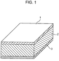
- Fig. 1 is a schematic view of a piezoelectric element according to an embodiment of the present invention.
- the piezoelectric element includes a first electrode 1, a piezoelectric material portion 2, and a second electrode 3.
- the piezoelectric material of the piezoelectric material portion 2 is a piezoelectric material according to an embodiment of the present invention.
- the piezoelectric property of the piezoelectric material can be evaluated by at least attaching the first electrode 1 and the second electrode 3 to the piezoelectric material portion 2 to form the piezoelectric element.
- Each of the first electrode 1 and the second electrode 3 is an electrically conductive layer having a thickness in the range of approximately 5 nm to 10 ⁇ m.
- the material of each of the first electrode 1 and the second electrode 3 is not particularly limited and may be any material that is commonly used for piezoelectric elements. Examples of such materials include metals, such as Ti, Pt, Ta, Ir, Sr, In, Sn, Au, Al, Fe, Cr, Ni, Pd, Ag, and Cu, and compounds thereof.
- the first electrode 1 and the second electrode 3 may be manufactured by any method, for example, by baking a metal paste or using a sputtering process or a vapor deposition method.
- the first electrode 1 and the second electrode 3 may have a desired pattern.
- the mechanical quality factor Qm of the piezoelectric element can be calculated from the resonance frequency and the antiresonant frequency measured with a commercially available impedance analyzer in accordance with a standard of Japan Electronics and Information Technology Industries Association (JEITA EM-4501). This method is hereinafter referred to as a resonance-antiresonance method.
- a multilayered piezoelectric element manufactured using a piezoelectric material according to an embodiment of the present invention will be described below.
- a multilayered piezoelectric element includes piezoelectric material layers and electrode layers alternately stacked on top of one another.
- the electrode layers include an internal electrode.
- the piezoelectric material layers include a piezoelectric material according to an embodiment of the present invention.
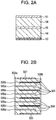
- FIGs. 2A and 2B are schematic cross-sectional views of a multilayered piezoelectric element according to an embodiment of the present invention.
- a multilayered piezoelectric element according to an embodiment of the present invention includes piezoelectric material layers 54 and electrode layers including an internal electrode 55.
- the multilayered piezoelectric element includes the piezoelectric material layers 54 and the layered electrodes alternately stacked on top of one another.
- the piezoelectric material layers 54 are made of the piezoelectric material described above.
- the electrodes may include external electrodes, such as a first electrode 51 and a second electrode 53, as well as the internal electrode 55.
- Fig. 2A illustrates the structure of a multilayered piezoelectric element according to an embodiment of the present invention.
- the multilayered piezoelectric element includes a layered body 56 between the first electrode 51 and the second electrode 53.
- the layered body 56 includes two piezoelectric material layers 54 with the internal electrode 55 interposed therebetween.
- the numbers of piezoelectric material layers and internal electrodes are not particularly limited and may be increased, as illustrated in Fig. 2B .
- the multilayered piezoelectric element illustrated in Fig. 2B includes a layered body between a first electrode 501 and a second electrode 503.
- the layered body includes nine piezoelectric material layers 504 and eight internal electrodes 505 (505a and 505b) alternately stacked on top of one another.
- the multilayered piezoelectric element further includes an external electrode 506a and an external electrode 506b for connecting the internal electrodes to each other.
- Each of the internal electrodes 55 and 505, the external electrodes 506a and 506b, the first electrodes 51 and 501, and the second electrodes 53 and 503 is an electrically conductive layer having a thickness in the range of approximately 5 to 2000 nm.
- the material of each of the electrodes is not particularly limited and may be any material that is commonly used for piezoelectric elements. Examples of such a material include metals, such as Ti, Pt, Ta, Ir, Sr, In, Sn, Au, Al, Fe, Cr, Ni, Pd, Ag, and Cu, and compounds thereof.
- Each of the internal electrodes 55 and 505 and the external electrodes 506a and 506b may be made of one of these materials or a mixture or an alloy thereof or may be a multilayer made of two or more of the materials. These electrodes may be made of different materials.
- the internal electrodes 55 and 505 may contain at least one of Ni and Cu, which are inexpensive electrode materials. When the internal electrodes 55 and 505 contain at least one of Ni and Cu, the multilayered piezoelectric element may be baked in a reducing atmosphere.
- the internal electrode 55 and the internal electrodes 505 of the multilayered piezoelectric element may contain Ag and Pd.
- the weight ratio M1/M2 of the weight M1 of Ag to the weight M2 of Pd is preferably in the range of 1.5 ⁇ M1/M2 ⁇ 9.0, more preferably 2.3 ⁇ M1/M2 ⁇ 4.0.
- a weight ratio M1/M2 of less than 1.5 is undesirable because of a high sintering temperature of the internal electrode(s).
- a weight ratio M1/M2 of more than 9.0 is also undesirable because the internal electrode(s) has an island structure and a heterogeneous surface.
- the plurality of electrodes including the internal electrodes 505 may be connected to each other in order to synchronize the driving voltage phases.
- the internal electrodes 505a may be connected to the first electrode 501 through the external electrode 506a.
- the internal electrodes 505b may be connected to the second electrode 503 through the external electrode 506b.
- the electrodes may be connected by any method.
- an electrode or an electric wire for connection may be disposed on a side surface of the multilayered piezoelectric element.
- a through-hole passing through the piezoelectric material layers 504 may be formed, and the inside of the through-hole may be coated with an electrically conductive material to connect the electrodes.
- a liquid discharge head includes a liquid chamber and a discharge port in communication with the liquid chamber.
- the liquid chamber has a vibrating portion that includes a piezoelectric element or a multilayered piezoelectric element according to an embodiment of the present invention.
- a liquid to be discharged from a liquid discharge head according to an embodiment of the present invention may be any fluid, for example, an aqueous liquid or a nonaqueous liquid, such as water, an ink, or a fuel.
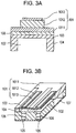
- Fig. 3B is a schematic view of the liquid discharge head.
- the liquid discharge head includes a discharge port 105, an individual liquid chamber 102, a communicating hole 106 that connects the individual liquid chamber 102 to the discharge port 105, a liquid chamber partition wall 104, a common liquid chamber 107, a diaphragm 103, and the piezoelectric element 101.
- the piezoelectric element 101 is rectangular in Fig. 3B
- the piezoelectric element 101 may be of another shape, such as elliptical, circular, or parallelogrammic.
- the piezoelectric material 1012 has a shape corresponding to the shape of the individual liquid chamber 102.
- Fig. 3A is a cross-sectional view of Fig. 3B in the width direction of the piezoelectric element.
- the piezoelectric element 101 may have a trapezoidal or inverted trapezoidal cross section.
- the first electrode 1011 is a lower electrode
- the second electrode 1013 is an upper electrode.
- the first electrode 1011 and the second electrode 1013 may be arranged differently.
- the first electrode 1011 may be a lower electrode or an upper electrode.
- the second electrode 1013 may be an upper electrode or a lower electrode.
- a buffer layer 108 may be disposed between the diaphragm 103 and the lower electrode.
- the diaphragm 103 bends upward and downward with the expansion and contraction of the piezoelectric material 1012, thereby applying pressure to a liquid in the individual liquid chamber 102. This allows the liquid to be discharged from the discharge port 105.
- a liquid discharge head according to an embodiment of the present invention can be used in printers and in the manufacture of electronic equipment.
- the diaphragm 103 has a thickness of 1.0 ⁇ m or more and 15 ⁇ m or less, preferably 1.5 ⁇ m or more and 8 ⁇ m or less.
- the material of the diaphragm is not particularly limited and may be Si. Si of the diaphragm may be doped with boron or phosphorus.
- the buffer layer and the electrode on the diaphragm may constitute the diaphragm.
- the buffer layer 108 has a thickness of 5 nm or more and 300 nm or less, preferably 10 nm or more and 200 nm or less.
- the discharge port 105 has an equivalent circular diameter of 5 ⁇ m or more and 40 ⁇ m or less.
- the discharge port 105 may be circular, star-shaped, square, or triangular.
- the liquid discharge apparatus includes a stage configured to receive an object and the liquid discharge head.
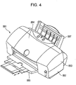
- the liquid discharge apparatus may be an ink jet recording apparatus, as illustrated in Figs. 4 and 5.
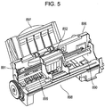
- Fig. 5 illustrates the liquid discharge apparatus (ink jet recording apparatus) 881 illustrated in Fig. 4 without exteriors 882 to 885 and 887.
- the ink jet recording apparatus 881 includes an automatic feeder 897 for automatically feeding a recording paper sheet as a transfer medium to the main body 896 of the apparatus.
- the ink jet recording apparatus 881 further includes a conveying unit 899 serving as a stage configured to receive an object, which conveys a recording paper sheet from the automatic feeder 897 to a predetermined recording position and from the recording position to an outlet 898, a recording unit 891 for recording to the recording paper at the recording position, and a recovering unit 890 for recovering the recording unit 891.
- the recording unit 891 includes a carriage 892 for housing a liquid discharge head according to an embodiment of the present invention. The carriage 892 travels along a rail.
- the carriage 892 travels along a rail in response to electric signals sent from a computer.
- the piezoelectric material Upon the application of a driving voltage to electrodes disposed on a piezoelectric material, the piezoelectric material is deformed.
- the piezoelectric material presses the individual liquid chamber 102 via the diaphragm 103 illustrated in Fig. 3B , thereby discharging an ink from the discharge port 105 to print characters.
- a liquid discharge apparatus can uniformly discharge a liquid at a high speed and can be reduced in size.
- a liquid discharge apparatus can be used in printing apparatuses, for example, ink jet recording apparatuses, such as facsimile machines, multifunction devices, and copying machines, industrial liquid discharge apparatuses, and drawing apparatuses for objects.
- ink jet recording apparatuses such as facsimile machines, multifunction devices, and copying machines
- industrial liquid discharge apparatuses such as facsimile machines, multifunction devices, and copying machines
- drawing apparatuses for objects.
- the liquid discharge head may move relative to a transfer medium disposed on a stage serving as a mounting portion.
- An ultrasonic motor includes a vibrating member and a moving body in contact with the vibrating member.
- the vibrating member includes a piezoelectric element or a multilayered piezoelectric element according to an embodiment of the present invention.
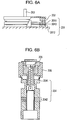
- Figs. 6A and 6B are schematic views of an ultrasonic motor according to an embodiment of the present invention.
- the ultrasonic motor illustrated in Fig. 6A includes a single plate of a piezoelectric element according to an embodiment of the present invention.
- the ultrasonic motor includes an oscillator 201, a rotor 202 pressed against a sliding surface of the oscillator 201 by the action of a pressure spring (not shown), and an output shaft 203, which is formed integrally with the rotor 202.
- the oscillator 201 includes a metal elastic ring 2011, a piezoelectric element 2012 according to an embodiment of the present invention, and an organic adhesive 2013 (epoxy or cyanoacrylate) that bonds the piezoelectric element 2012 to the elastic ring 2011.
- the piezoelectric element 2012 includes a piezoelectric material between a first electrode and a second electrode.
- a flexural traveling wave occurs in the oscillator 201, and points on the sliding surface of the oscillator 201 go through elliptical motion.
- the rotor 202 pressed against the sliding surface of the oscillator 201 receives friction force from the oscillator 201 and rotates in a direction opposite to the direction of the flexural traveling wave.
- a body to be driven (not shown) joined to the output shaft 203 is driven by the rotational force of the rotor 202.
- the piezoelectric material Upon the application of a voltage to a piezoelectric material, the piezoelectric material expands and contracts because of the transverse piezoelectric effect.
- An elastic body, such as a metal, joined to the piezoelectric element is bent with the expansion and contraction of the piezoelectric material.
- the ultrasonic motor described herein utilizes this principle.
- Fig. 6B illustrates an ultrasonic motor that includes a multilayered piezoelectric element.
- the oscillator 204 includes a multilayered piezoelectric element 2042 in a tubular metal elastic body 2041.
- the multilayered piezoelectric element 2042 includes a plurality of layered piezoelectric materials (not shown) and includes a first electrode and a second electrode on the outer surfaces of the layered piezoelectric materials and internal electrodes within the layered piezoelectric materials.
- the metal elastic body 2041 is fastened with a bolt to hold the piezoelectric element 2042, thereby constituting the oscillator 204.
- the oscillator 204 Upon the application of alternating voltages of different phases to the piezoelectric element 2042, the oscillator 204 causes two oscillations perpendicular to each other. The two oscillations are synthesized to form a circular oscillation for driving the tip of the oscillator 204.
- the oscillator 204 has an annular groove at its upper portion. The annular groove increases the oscillatory displacement for driving.
- a rotor 205 is pressed against the oscillator 204 by the action of a pressure spring 206 and receives friction force for driving.
- the rotor 205 is rotatably supported by a bearing.
- the optical apparatus includes a drive unit that includes the ultrasonic motor described above.
- Figs. 7A and 7B are cross-sectional views of an interchangeable lens barrel of a single-lens reflex camera, which is an optical apparatus according to an embodiment of the present invention.
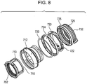
- Fig. 8 is an exploded perspective view of an interchangeable lens barrel of a single-lens reflex camera, which is an optical apparatus according to an embodiment of the present invention.
- a fixed barrel 712, a linear guide barrel 713, and a front lens group barrel 714 are fixed to a removable mount 711 of the camera. These components are fixed members of the interchangeable lens barrel.
- the linear guide barrel 713 has a linear guide groove 713a for a focus lens 702 in the optical axis direction.
- the focus lens 702 is supported by a rear lens group barrel 716.
- Cam rollers 717a and 717b protruding outwardly in the radial direction are fixed to the rear lens group barrel 716 with a screw 718.
- the cam roller 717a fits in the linear guide groove 713a.
- a cam ring 715 rotatably fits in the internal circumference of the linear guide barrel 713.
- a roller 719 fixed to the cam ring 715 is caught in an annular groove 713b of the linear guide barrel 713, thereby restricting the relative displacement of the linear guide barrel 713 and the cam ring 715 in the optical axis direction.
- the cam ring 715 has a cam groove 715a for the focus lens 702.
- the cam roller 717b also fits in the cam groove 715a.
- a rotation transmitting ring 720 is rotatably held by a ball race 727 at a fixed position on the periphery of the fixed barrel 712.
- a driven roller 722 is rotatably held by a shaft 720f extending radially from the rotation transmitting ring 720.
- a large-diameter portion 722a of the driven roller 722 is in contact with a mount side end face 724b of a manual focus ring 724.
- a small-diameter portion 722b of the driven roller 722 is in contact with a joint 729.
- Six driven rollers 722 are disposed at regular intervals on the periphery of the rotation transmitting ring 720. Each of the driven rollers 722 satisfies the structural relationship described above.
- a low-friction sheet (washer member) 733 is disposed on the inside of the manual focus ring 724.
- the low-friction sheet 733 is disposed between a mount side end face 712a of the fixed barrel 712 and a front end face 724a of the manual focus ring 724.
- the low-friction sheet 733 has a circular outer surface having a diameter that fits to the inner diameter 724c of the manual focus ring 724.
- the inner diameter 724c of the manual focus ring 724 fits to the diameter of an outer portion 712b of the fixed barrel 712.
- the low-friction sheet 733 can reduce friction in the rotating ring mechanism in which the manual focus ring 724 rotates about the optical axis relative to the fixed barrel 712.
- the large-diameter portion 722a of the driven roller 722 is pressed against the mount side end face 724b of the manual focus ring 724 because the wave washer 726 presses the ultrasonic motor 725 forward to the front of the lens. Likewise, because the wave washer 726 presses the ultrasonic motor 725 forward to the front of the lens, the small-diameter portion 722b of the driven roller 722 is pressed against the joint 729. The wave washer 726 is prevented from moving toward the mount by a washer 732 bayonet coupled to the fixed barrel 712.
- the spring force (impellent force) of the wave washer 726 is transmitted to the ultrasonic motor 725 and the driven roller 722 and furthermore presses the manual focus ring 724 against the mount side end face 712a of the fixed barrel 712.
- the manual focus ring 724 is pressed against the mount side end face 712a of the fixed barrel 712 via the low-friction sheet 733.
- the driven roller 722 rotates about the shaft 720f because the joint 729 is in frictional contact with the small-diameter portion 722b of the driven roller 722.
- the rotation of the driven roller 722 about the shaft 720f causes the rotation of the rotation transmitting ring 720 about the optical axis (automatic focusing).
- a manual input unit (not shown) provides the manual focus ring 724 with rotational force about the optical axis
- the driven roller 722 is rotated about the shaft 720f because of friction force.
- the rotation of the large-diameter portion 722a of the driven roller 722 about the shaft 720f causes the rotation of the rotation transmitting ring 720 about the optical axis.
- the ultrasonic motor 725 is not rotated because of the friction force between a rotor 725c and a stator 725b (manual focusing).
- the rotation transmitting ring 720 is provided with two focus keys 728 facing each other. These focus keys 728 fit into notches 715b at the tip of the cam ring 715.
- the rotation transmitting ring 720 is rotated about the optical axis, and the rotational force is transmitted to the cam ring 715 via the focus keys 728.
- the cam roller 717b moves the cam roller 717a and the rear group lens barrel 716 restricted by the linear guide groove 713a forward or backward along the cam groove 715a of the cam ring 715. This drives the focus lens 702 and allows focusing.
- optical apparatus may also be applied to optical apparatuses that include an ultrasonic motor in a drive unit, for example, cameras, such as compact cameras, electronic still cameras, and personal digital assistants including a camera.
- Vibratory apparatuses for conveying or removing particles, powders, and droplets are widely used in electronic equipment.
- a vibratory apparatus includes a vibrating member that includes the piezoelectric element or the multilayered piezoelectric element described above disposed on a diaphragm.
- the dust removing device includes a vibrating portion that includes the vibratory apparatus described above.
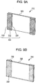
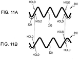
- Figs. 9A and 9B are schematic views of a dust removing device 310 according to an embodiment of the present invention.
- the dust removing device 310 includes a plate of the piezoelectric element 330 and the diaphragm 320.
- the piezoelectric element 330 may be a multilayered piezoelectric element according to an embodiment of the present invention.
- the diaphragm 320 may be made of any material. When the dust removing device 310 is used in optical devices, the diaphragm 320 may be made of a translucent or transparent material or a light reflective material.
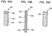
- Figs. 10A to 10C are schematic views of the piezoelectric element 330 illustrated in Figs. 9A and 9B .
- Figs. 10A and 10C illustrate the front and back sides of the piezoelectric element 330.
- Fig. 10B is a side view of the piezoelectric element 330.
- the piezoelectric element 330 includes a piezoelectric material 331, a first electrode 332, and a second electrode 333.
- the first electrode 332 and the second electrode 333 are disposed on opposite sides of the piezoelectric material 331.
- Figs. 10A to 10C are schematic views of the piezoelectric element 330 illustrated in Figs. 9A and 9B .
- Figs. 10A and 10C illustrate the front and back sides of the piezoelectric element 330.
- Fig. 10B is a side view of the piezoelectric element 330.
- the piezoelectric element 330 includes a piezoelectric material 331, a first
- the piezoelectric element 330 may be a multilayered piezoelectric element according to an embodiment of the present invention.
- the piezoelectric material 331 includes piezoelectric material layers and internal electrodes alternately stacked on top of one another. The internal electrodes are alternately connected to the first electrode 332 and the second electrode 333, thereby allowing the piezoelectric material layers to alternately have a drive waveform of a different phase.
- a surface of the piezoelectric element 330 on which the first electrode 332 is disposed is referred to as a first electrode surface 336.
- a surface of the piezoelectric element 330 on which the second electrode 333 is disposed is referred to as a second electrode surface 337.
- electrode surface refers to a surface of a piezoelectric element on which an electrode is disposed.
- the first electrode 332 may round a corner and extends to the second electrode surface 337.
- the first electrode surface 336 of the piezoelectric element 330 is bonded to the diaphragm 320.
- Actuation of the piezoelectric element 330 produces a stress between the piezoelectric element 330 and the diaphragm 320, causing out-of-plane oscillations on the diaphragm 320.
- the dust removing device 310 removes foreign matter, such as dust, on the diaphragm 320 by the action of out-of-plane oscillations.
- the term "out-of-plane oscillations" refers to elastic oscillations that cause displacements of a diaphragm in the optical axis direction or the diaphragm thickness direction.
- Figs. 11A and 11B are schematic views illustrating the vibration principle of the dust removing device 310.
- in-phase alternating voltages are applied to a left-and-right pair of the piezoelectric elements 330 to cause out-of-plane oscillations of the diaphragm 320.
- the direction of polarization of the piezoelectric material constituting the left-and-right pair of the piezoelectric elements 330 is the same as the thickness direction of the piezoelectric elements 330.
- the dust removing device 310 is driven in a seventh oscillation mode.
- Fig. 11A in-phase alternating voltages are applied to a left-and-right pair of the piezoelectric elements 330 to cause out-of-plane oscillations of the diaphragm 320.
- the direction of polarization of the piezoelectric material constituting the left-and-right pair of the piezoelectric elements 330 is the same as the thickness direction of the piezoelectric elements 330.
- the image pickup apparatus includes the dust removing device and an image pickup element unit, wherein the dust removing device includes a diaphragm on the light-receiving surface of the image pickup element unit.
- Figs. 12 and 13 illustrate a digital single-lens reflex camera, which is an image pickup apparatus according to an embodiment of the present invention.
- Fig. 12 is a front perspective view of the main body 601 of the camera viewed from the object side. An imaging lens unit has been removed.
- Fig. 13 is an exploded perspective view of the inside of the camera, illustrating surrounding structures of a dust removing device according to an embodiment of the present invention and an image pickup unit 400.
- the main body 601 of the camera includes a mirror box 605 to which an image light beam passing through an imaging lens is directed.
- the mirror box 605 includes a main mirror (quick return mirror) 606.
- the main mirror 606 can make an angle of 45 degrees with the optical axis to direct an image light beam to a penta roof mirror (not shown) or may avoid the image light beam in order to direct the image light beam to an image pickup element (not shown).
- the mirror box 605 and a shutter unit 200 are disposed in front of a main body chassis 300 of the main body 601 of the camera in this order from the object side.
- the image pickup unit 400 is disposed on the photographer side of the main body chassis 300.
- the image pickup unit 400 is installed such that an image pickup surface of the image pickup element is disposed at a predetermined distance from and parallel to the surface of a mount 602 to which an imaging lens unit is to be attached.
- the image pickup apparatus may be an interchangeable-lens camera, such as a mirrorless digital interchangeable-lens camera without the mirror box 605.
- an image pickup apparatus according to an embodiment of the present invention can particularly be applied to devices that require the removal of dust deposited on a surface of an optical component.
- Fig. 14 is a perspective view of the main body 931 of a digital camera, which is electronic equipment according to an embodiment of the present invention.
- An optical device 901, a microphone 914, an electronic flash unit 909, and a fill light unit 916 are disposed on the front surface of the main body 931.
- the microphone 914 is disposed within the main body and is indicated by a broken line.
- An opening for catching external sound is disposed in front of the microphone 914.
- a power switch 933, a loudspeaker 912, a zoom lever 932, and a release button 908 for focusing are disposed on the top surface of the main body 931.
- the loudspeaker 912 is disposed within the main body 931 and is indicated by a broken line.
- An opening for transmitting sound to the outside is disposed in front of the loudspeaker 912.
- the piezoelectric acoustic component may be used in at least one of the microphone 914, the loudspeaker 912, and a surface acoustic wave device.
- the electronic equipment may also be applied to electronic equipment that includes a piezoelectric acoustic component, such as audio-reproducing devices, audio-recording devices, mobile phones, and information terminals.
- a piezoelectric acoustic component such as audio-reproducing devices, audio-recording devices, mobile phones, and information terminals.
- a piezoelectric element and a multilayered piezoelectric element according to an embodiment of the present invention are suitable for liquid discharge heads, liquid discharge apparatuses, ultrasonic motors, optical apparatuses, vibratory apparatuses, dust removing devices, image pickup apparatuses, and electronic equipment.
- a liquid discharge head manufactured by using a piezoelectric element or a multilayered piezoelectric element according to an embodiment of the present invention can have a nozzle density and a discharge velocity higher than or equal to those of liquid discharge heads manufactured by using a lead-containing piezoelectric element.
- a liquid discharge apparatus manufactured by using a liquid discharge head according to an embodiment of the present invention can have a discharge velocity and discharge accuracy higher than or equal to those of liquid discharge apparatuses manufactured by using a lead-containing piezoelectric element.
- An ultrasonic motor manufactured by using a piezoelectric element or a multilayered piezoelectric element according to an embodiment of the present invention can have driving force and durability higher than or equal to those of ultrasonic motors manufactured by using a lead-containing piezoelectric element.
- An optical apparatus manufactured by using an ultrasonic motor according to an embodiment of the present invention can have durability and operation accuracy higher than or equal to those of optical apparatuses manufactured by using a lead-containing piezoelectric element.
- a vibratory apparatus manufactured by using a piezoelectric element or a multilayered piezoelectric element according to an embodiment of the present invention can have vibratory capacity and durability higher than or equal to those of ultrasonic motors manufactured by using a lead-containing piezoelectric element.
- a dust removing device manufactured by using a vibratory apparatus can have dust removal efficiency and durability higher than or equal to those of dust removing devices manufactured by using a lead-containing piezoelectric element.
- An image pickup apparatus manufactured by using a dust removing device can have a dust removal function higher than or equal to those of image pickup apparatuses manufactured by using a lead-containing piezoelectric element.
- a piezoelectric acoustic component that includes a piezoelectric element or a multilayered piezoelectric element according to an embodiment of the present invention can be used to provide electronic equipment that has sound production ability higher than or equal to those of electronic equipment manufactured by using a lead-containing piezoelectric element.
- a piezoelectric material according to an embodiment of the present invention may be used in ultrasonic transducers, piezoelectric actuators, piezoelectric sensors, and ferroelectric memories, as well as liquid discharge heads and motors.
- Table 1 shows the compositions of piezoelectric materials according to Examples 1 to 42 and sintered bodies according to Comparative Examples 1 to 9 of the present invention.
- Table 1 Sample RE x' x y z (mol%) w (mol%) Comparative example 1 None 0.88 0.86 0.88 0 0
- Example 1 La 0.88 0.86 0.88 0.25 0.50
- Example 2 La 0.88 0.86 0.88 0.75 0.50
- Example 3 La 0.88 0.86 0.88 5.00 0.50
- Comparative example 2 La 0.88 0.86 0.88 6.00 0.50
- Example 5 La 0.88 0.86 0.85 0.75 0.50
- Example 6 La 0.95 0.93 0.95 0.75 0.50
- Example 7 La 0.88 0.86 0.88 0.25 0
- Example 8 La 0.88 0.86 0.88 0.25 0.20
- Example 9 La 0.88 0.86 0.88 0.25 2.00 Comparative example 4 La 0.97 0.95 0.97 0.50
- the raw materials included powders of at least 99% pure sodium niobate (NaNbO 3 ), 99.95% pure barium carbonate (BaCO 3 ), at least 99% pure barium titanate (BaTiO 3 ), 99.9% pure copper oxide (Cu(II)O), and 99% pure sodium carbonate (Na 2 CO 3 ).
- a rare earth material represented by RE 2 O 3 (RE denotes at least one element selected from La, Pr, Nd, Pm, Sm, Eu, Gd, Tb, Dy, Ho, Er, Tm, Yb, and Lu) was a powder of at least 99% purity.
- the raw material of La was at least 99% pure La 2 O 3 .
- the La content of 0.25 mol% in Example 1 means that the weight of La 2 O 3 was 0.815 g (0.695 g of La) per mol of the perovskite-type metal oxide having the general formula (1) (171.75 g).
- Example 1 the raw materials were mixed such that the Cu (w) content corresponded to 0.50 mol% of the perovskite-type metal oxide.
- the raw material of Cu was 99.9% pure copper oxide (Cu(II)O).
- the Cu content of 0.50 mol% in Example 1 means that the weight of copper oxide was 0.398 g (0.317 g of Cu) per mol of the perovskite-type metal oxide having the general formula (1) (171.75 g).
- the mixed powder was calcined in the ambient atmosphere at a temperature in the range of 900°C to 1100°C for 2 to 5 hours.
- the calcined powder was pulverized and was granulated with a PVB binder.
- the weight of the PVB binder corresponded to 3% by weight of the calcined powder.
- the granulated powder was charged into a mold and was compressed at a pressure of 200 MPa, yielding a compact having a diameter of 17 mm and a thickness of approximately 1 mm.
- the compact was fired in the air at a temperature in the range of 1150°C to 1300°C for 2 to 6 hours to yield a sintered body.
- the density of the sintered body was measured using Archimedes' principle, and the relative density was calculated.
- the sintered bodies of the examples and the comparative examples had a relative density of 94% or more.
- the density of the samples containing Cu was 1% to 3% higher than the density of the samples having the same composition but not containing Cu.
- the addition of Cu reduced the calcination and firing temperatures by 50°C to 100°C.
- the sintered body was polished to a thickness of approximately 0.5 mm.
- the constituent phase and the lattice constant of the polished sintered body or a powder of the polished sintered body was determined by X-ray diffraction.
- the X-ray diffraction showed that the samples were substantially composed of a single phase of the perovskite structure.
- the composition of the sintered body was analyzed by inductively coupled plasma emission spectroscopy (ICP).
- Table 1 shows the results as x and y of the general formula (1) and RE (z) and Cu (w).
- the value x in Table 1 represents the molar ratio of Na in the sintered body.
- the value x' represents the molar ratio of Na in the raw materials.
- the value x in Table 1 denotes the molar ratio of Na. In all the samples, the molar ratio of Na was lower than the predictive value. The elements other than Na had the expected composition. The molar ratio (x/y) of Na (x) to Nb (y) was in the range of 94% to 98% except for Examples 5 and 18, indicating the deficiency of Na. The Cu content was low and therefore had a measurement error of ⁇ 50% in Table 1. The grain size of the sintered body was determined through observation with an optical microscope or an electron microscope.
- the sintered body had an average grain size in the range of 2 to 50 ⁇ m as measured with an electron microscope.
- the distribution of Cu in the sintered body was examined by energy dispersive X-ray spectroscopy. Most of added Cu was distributed in grain boundaries, and a small portion of Cu was present in the grains.
- piezoelectric elements were manufactured with the piezoelectric materials according to Examples 1 to 42.
- the polished sintered body was heat-treated in the air at a temperature in the range of 400°C to 500°C for 30 minutes.
- a gold electrode having a thickness of 400 nm was formed on the front and back sides of the polished sintered body by DC sputtering.
- a titanium film having a thickness of 30 nm was formed as an adhesion layer between the electrode and the sintered body.
- the sintered body having the electrode was cut to prepare a plate-like piezoelectric element 10 mm in length, 2.5 mm in width, and 0.5 mm in thickness.
- Resistivity was measured with a semiconductor parameter analyzer. A direct-current voltage of several tens to a hundred volts was applied to a sample, and the electrical resistance was measured 30 seconds after the start of voltage application. Resistivity was calculated from the measured electrical resistance and the dimensions of the sample. When the resistivity is 30 G ⁇ cm or more, preferably 100 G ⁇ cm or more, the piezoelectric material and the piezoelectric element have a satisfactory practical insulation property.
- Polarization treatment was performed before the evaluation of the piezoelectric property. More specifically, a voltage in the range of 1.5 to 5 kV/mm was applied to a sample in an oil bath at 150°C for 30 minutes, and the sample was cooled to room temperature while the voltage was maintained.
- the mechanical quality factor Qm of the plate-like piezoelectric element was measured using a resonance-antiresonance method.
- the piezoelectric constant (d 33 ) of the sample was measured with a Berlincourt d 33 meter. Dielectric loss was measured with an impedance analyzer in an environmental test box at -20°C. The measurement frequency was 1 kHz, and the applied alternating voltage was 500 mV. Measurement was performed after polarization treatment.
- the temperature dependence of the relative dielectric constant was measured from room temperature.
- the change in relative dielectric constant was measured while a sample was cooled from room temperature to -100°C and was then heated to 350°C.
- the Curie temperature was calculated from the maximum relative dielectric constant.
- the samples had a Curie temperature of 150°C or more.
- Table 2 shows the evaluation results of the samples.
- Table 2 Sample Piezoelectric constant d 33 (pC/N) Mechanical quality factor Qm (-) Resistivity (G ⁇ cm) Dielectric loss (%) Comparative example 1 145 170 5 1.5 Example 1 151 301 115 0.8 Example 2 140 310 220 0.6 Example 3 102 318 291 0.5 Comparative example 2 75 304 230 0.5 Comparative example 3 95 291 7 1.1 Example 4 117 300 101 0.6 Example 5 108 298 35 0.9 Example 6 101 303 106 0.6 Example 7 125 180 34 0.8 Example 8 138 225 119 0.9 Example 9 131 412 330 0.7 Comparative example 4 86 306 260 0.6 Example 10 148 287 118 0.8 Example 11 137 295 198 0.6 Example 12 150 288 116 0.8 Example 13 136 302 201 0.6 Example 14 149 298 113 0.8 Example 15 137 305 212 0.6 Example 16 109 309 288 0.5 Comparative example 5 74 2
- Comparative Example 1 which did not contain a rare-earth element and Cu, had a low electrical resistance and a significant dielectric loss. Comparative Example 2, which had a La content of 6 mol%, had a piezoelectric constant d 33 of less than 100 pC/N.
- Comparative Example 3 which had x as low as 0.75, had a low electrical resistance and a significant dielectric loss.
- Comparative Example 4 which had y as large as 0.97, had a piezoelectric constant d 33 of less than 100 pC/N.
- Comparative Example 5 which had a Dy content of 6 mol%, had a piezoelectric constant d 33 of less than 100 pC/N.
- Comparative Example 6 which had x as low as 0.75, had a low electrical resistance and a significant dielectric loss.
- Comparative Examples 7 and 8 which contained no rare-earth element, had a low electrical resistance and a significant dielectric loss.
- Comparative Example 9 which had y as large as 0.97, had a piezoelectric constant d 33 of less than 100 pC/N.
- All the samples according to the examples had a piezoelectric constant d 33 of 100 pC/N or more, a resistivity of more than 30 G ⁇ cm, and a dielectric loss of less than 1.0%.
- Example 1 The raw materials corresponding to Example 1 were weighed as described below.
- Powders of sodium carbonate (Na 2 CO 3 ), niobium oxide (Nb 2 O 5 ), barium titanate (BaTiO 3 ), lanthanum oxide (La 2 O 3 ), and copper oxide (CuO) were weighed such that Na, Nb, Ba, Ti, La, and Cu satisfied the composition of Example 1 described in Table 1.
- the weighed raw powders were mixed in a ball mill overnight and was calcined at a temperature in the range of 1000°C to 1100°C to yield a calcined powder.
- the calcined powder was mixed with a solvent, a binder (PVB), and a plasticizer (dibutyl phthalate) to prepare a slurry.
- the slurry was formed into a green sheet having a thickness of 50 ⁇ m using a doctor blade method.
- Nine of the green sheets to which the electrically conductive paste had been applied were stacked and were fired at 1150°C for 5 hours to yield a sintered body.
- the sintered body was cut into a 10 mm x 2.5 mm piece. The side surfaces of the piece were polished.
- a pair of external electrodes (a first electrode and a second electrode) for alternately connecting internal electrodes were formed by Au sputtering.
- a multilayered piezoelectric element as illustrated in Fig. 2B was manufactured.
- a sample was subjected to polarization treatment. More specifically, the sample was heated to 150°C in an oil bath. While a voltage of 2 kV/mm was applied between the first electrode and the second electrode for 30 minutes, the sample was cooled to room temperature.
- the evaluation of the piezoelectricity of the multilayered piezoelectric element showed that the multilayered piezoelectric element had a satisfactory insulation property and had a satisfactory piezoelectric property similar to the piezoelectric material according to Example 1.
- Powders of sodium niobate (NaNbO 3 ), barium titanate (BaTiO 3 ), lanthanum oxide (La 2 O 3 ), and copper oxide (CuO) were weighed such that Na, Nb, Ba, Ti, La, and Cu satisfied the composition of Example 2 described in Table 1.
- the weighed raw powders were mixed in a ball mill overnight and was calcined at a temperature in the range of 1000°C to 1100°C to yield a calcined powder.
- the calcined powder was mixed with a solvent, a binder (PVB), and a plasticizer (dibutyl phthalate) to prepare a slurry.
- the slurry was formed into a green sheet having a thickness of 50 ⁇ m using a doctor blade method.
- An electrically conductive paste for an internal electrode was applied to the green sheet.
- the electrically conductive paste was a Ni paste.
- the heat-pressed layered body was fired in a tubular furnace.
- the sintered body was cut into a 10 mm x 2.5 mm piece.
- the side surfaces of the piece were polished.
- a pair of external electrodes (a first electrode and a second electrode) for alternately connecting internal electrodes were formed by Au sputtering.
- a multilayered piezoelectric element as illustrated in Fig. 2B was manufactured.
- the observation of the internal electrodes of the multilayered piezoelectric element showed that the electrode material (electrode layer) Ni and piezoelectric material layers were alternately stacked on top of one another.
- An electric field of 2 kV/mm was applied to the multilayered piezoelectric element in an oil bath at 150°C for 30 minutes for polarization treatment.
- the evaluation of the piezoelectric property of the multilayered piezoelectric element showed that the multilayered piezoelectric element had a satisfactory insulation property and had a satisfactory piezoelectric property similar to the piezoelectric element according to Example 2.
- a liquid discharge head illustrated in Figs. 3A and 3B was manufactured using the piezoelectric element according to Example 14. An ink was discharged in response to the input of an electric signal.
- a liquid discharge apparatus illustrated in Fig. 4 was manufactured using the liquid discharge head according to Example 45. An ink was discharged and deposited onto a recording medium in response to the input of an electric signal.
- An ultrasonic motor illustrated in Fig. 6A was manufactured using the piezoelectric element according to Example 14. Upon the application of an alternating voltage, the motor rotated.
- FIG. 7A and 7B An optical apparatus illustrated in Figs. 7A and 7B was manufactured using the ultrasonic motor according to Example 47. Upon the application of an alternating voltage, automatic focusing was observed.
- a dust removing device illustrated in Figs. 9A and 9B was manufactured using the piezoelectric element according to Example 14. Upon the application of an alternating voltage after plastic beads were scattered, satisfactory dust removing efficiency was observed.
- An image pickup apparatus illustrated in Fig. 12 was manufactured using the dust removing device according to Example 49. Dust on the surface of the image pickup unit was satisfactorily removed, and images free of dust defects were obtained.
- Liquid discharge heads illustrated in Figs. 3A and 3B were manufactured using the multilayered piezoelectric elements according to Examples 43 and 44. An ink was discharged in response to the input of an electric signal.
- Liquid discharge apparatuses illustrated in Fig. 4 were manufactured using the liquid discharge heads according to Example 51. An ink was discharged and deposited onto a recording medium in response to the input of an electric signal.
- Ultrasonic motors illustrated in Fig. 6B were manufactured using the multilayered piezoelectric elements according to Examples 43 and 44. Upon the application of an alternating voltage, the motors rotated.
- Optical apparatuses illustrated in Figs. 7A and 7B were manufactured using the ultrasonic motors according to Example 53. Upon the application of an alternating voltage, automatic focusing was observed.
- Dust removing devices illustrated in Figs. 9A and 9B were manufactured using the multilayered piezoelectric elements according to Examples 43 and 44. Upon the application of an alternating voltage after plastic beads were scattered, satisfactory dust removing efficiency was observed.
- Image pickup apparatuses illustrated in Fig. 12 were manufactured using the dust removing devices according to Example 55. Dust on the surface of the image pickup unit was satisfactorily removed, and images free of dust defects were obtained.
- Electronic equipment illustrated in Fig. 14 was manufactured using the multilayered piezoelectric elements according to Examples 43 and 44. Upon the application of an alternating voltage, a loudspeaker operated.
- a piezoelectric material according to an embodiment of the present invention has satisfactory piezoelectricity even at high environmental temperatures.
- a piezoelectric material according to an embodiment of the present invention contains no lead and can reduce the load on the environment.
- a piezoelectric material according to an embodiment of the present invention can be efficiently used also for apparatuses manufactured using a large amount of piezoelectric material, such as liquid discharge heads, ultrasonic motors, and dust removing devices.
Landscapes
- Engineering & Computer Science (AREA)
- Chemical & Material Sciences (AREA)
- Ceramic Engineering (AREA)
- Physics & Mathematics (AREA)
- Manufacturing & Machinery (AREA)
- Materials Engineering (AREA)
- General Physics & Mathematics (AREA)
- Optics & Photonics (AREA)
- Structural Engineering (AREA)
- Organic Chemistry (AREA)
- Inorganic Chemistry (AREA)
- Mechanical Engineering (AREA)
- Signal Processing (AREA)
- Multimedia (AREA)
- Particle Formation And Scattering Control In Inkjet Printers (AREA)
- General Electrical Machinery Utilizing Piezoelectricity, Electrostriction Or Magnetostriction (AREA)
- Compositions Of Oxide Ceramics (AREA)
Claims (15)
- Matériau piézoélectrique, comprenant : un oxyde métallique de type pérovskite ayant la formule générale (1) suivante :
(NaxBa1-y) (NbyTi1-y)O3 (1)
(dans laquelle x satisfait 0,80 ≤ x ≤ 0,95, et y satisfait 0,85 ≤ y ≤ 0,95)
et caractérisé en ayant de plus au moins un élément de terre rare choisi parmi La, Pr, Nd, Pm, Sm, Eu, Gd, Tb, Dy, Ho, Er, Tm, Yb et Lu, où la teneur en élément de terre rare est de plus de 0,25 % en mole et 5 % en moles ou moins de la quantité d'oxyde métallique de type pérovskite. - Matériau piézoélectrique selon la revendication 1, comprenant en outre du Cu, où une teneur du Cu est de plus de 0 % en mole et de 2 % en moles ou moins de la quantité d'oxyde métallique de type pérovskite.
- Matériau piézoélectrique selon la revendication 1 ou 2, dans lequel x est plus petit que y dans la formule générale (1).
- Élément piézoélectrique, comprenant : une première électrode ; une partie de matériau piézoélectrique ; et une seconde électrode, où la partie de matériau piézoélectrique comprend le matériau piézoélectrique selon l'une quelconque des revendications 1 à 3.
- Élément piézoélectrique multicouche, comprenant : des couches de matériau piézoélectrique et des couches d'électrode empilées en alternance au sommet l'une de l'autre, les couches d'électrode comprenant une électrode interne, où les couches de matériau piézoélectrique comprennent le matériau piézoélectrique selon l'une quelconque des revendications 1 à 3.
- Élément piézoélectrique multicouche selon la revendication 5, dans lequel l'électrode interne contient Ag et Pd, et le rapport en poids M1/M2 du poids M1 d'Ag au poids M2 de Pd se situe dans la plage de 1,5 ≤ M1/M2 ≤ 9,0.
- Élément piézoélectrique multicouche selon la revendication 5, dans lequel l'électrode interne contient au moins un de Ni et de Cu.
- Tête de déchargement de liquide, comprenant : une 5 chambre de liquide ; et une porte de déchargement en communication avec la chambre de liquide, où la chambre de liquide a une partie vibratoire qui comprend l'élément piézoélectrique selon la revendication 4 ou l'élément piézoélectrique multicouche selon l'une quelconque des 10 revendications 5 à 7.
- Appareil de déchargement de liquide, comprenant : une phase configurée pour recevoir un objet ; et la tête de déchargement de liquide selon la revendication 8.
- Moteur ultrasonore, comprenant : un élément 15 vibratoire qui comprend l'élément piézoélectrique selon la revendication 4 ou l'élément piézoélectrique multicouche selon l'une quelconque des revendications 5 à 7 ; et un corps amovible en contact avec l'élément vibratoire.
- Appareil optique, qui comprend une unité de 20 direction qui comprend le moteur ultrasonore selon la revendication 10.
- Appareil vibratoire, comprenant un élément vibratoire qui comprend l'élément piézoélectrique selon la revendication 4 ou l'élément piézoélectrique multicouche selon l'une quelconque des revendications 5 à 7 sur un diaphragme.
- Dispositif éliminant la poussière, comprenant une partie vibratoire comprenant l'appareil vibratoire selon la revendication 12.
- Appareil d'acquisition d'images, comprenant : le dispositif éliminant la poussière selon la revendication 13 ; et une unité d'élément d'acquisition d'images, où le diaphragme du dispositif éliminant la poussière est disposé sur le côté de surface recevant la lumière de l'unité 35 d'élément d'acquisition d'images.
- Équipement électronique, comprenant un composant acoustique piézoélectrique qui comprend l'élément piézoélectrique selon la revendication 4 ou l'élément piézoélectrique multicouche selon l'une quelconque des 5 revendications 5 à 7.
Applications Claiming Priority (2)
| Application Number | Priority Date | Filing Date | Title |
|---|---|---|---|
| JP2013014613 | 2013-01-29 | ||
| PCT/JP2014/052186 WO2014119703A1 (fr) | 2013-01-29 | 2014-01-24 | Matériau piézoélectrique, élément piézoélectrique et équipement électronique |
Publications (2)
| Publication Number | Publication Date |
|---|---|
| EP2946417A1 EP2946417A1 (fr) | 2015-11-25 |
| EP2946417B1 true EP2946417B1 (fr) | 2017-06-07 |
Family
ID=50150744
Family Applications (1)
| Application Number | Title | Priority Date | Filing Date |
|---|---|---|---|
| EP14705586.7A Active EP2946417B1 (fr) | 2013-01-29 | 2014-01-24 | Matériau piézoélectrique, élément piézoélectrique et équipement électronique |
Country Status (5)
| Country | Link |
|---|---|
| US (2) | US9932273B2 (fr) |
| EP (1) | EP2946417B1 (fr) |
| JP (1) | JP6366284B2 (fr) |
| TW (1) | TW201434789A (fr) |
| WO (1) | WO2014119703A1 (fr) |
Families Citing this family (14)
| Publication number | Priority date | Publication date | Assignee | Title |
|---|---|---|---|---|
| EP2867929B1 (fr) * | 2012-08-27 | 2016-11-30 | Canon Kabushiki Kaisha | Matériau piézoélectrique |
| EP2873103B1 (fr) * | 2012-08-27 | 2020-10-28 | Canon Kabushiki Kaisha | Matériau piézoélectrique et élément piézoélectrique utilisant ledit matériau piézoélectrique, et appareil électronique utilisant l'élément piézoélectronique |
| EP2936576B1 (fr) * | 2012-12-21 | 2017-03-15 | Canon Kabushiki Kaisha | Dispositif d'entraînement à onde vibratoire, dispositif de prise d'images, appareil optique, dispositif de déversement de liquide, et appareil électronique |
| JPWO2017018222A1 (ja) * | 2015-07-24 | 2018-06-07 | 株式会社ユーテック | 圧電体膜及びその製造方法、バイモルフ素子、圧電体素子及びその製造方法 |
| KR101792381B1 (ko) * | 2016-01-04 | 2017-11-01 | 삼성전기주식회사 | 전자부품 및 그 제조방법 |
| JP2017179416A (ja) * | 2016-03-29 | 2017-10-05 | Tdk株式会社 | 圧電磁器スパッタリングターゲット、非鉛圧電薄膜およびそれを用いた圧電薄膜素子 |
| USD857020S1 (en) * | 2016-05-25 | 2019-08-20 | Tdk Corporation | Piezoelectric element |
| JP1565481S (fr) * | 2016-05-25 | 2016-12-19 | ||
| US10069061B2 (en) * | 2016-06-02 | 2018-09-04 | eLux Inc. | Fabrication and harvest of piezoelectric plates |
| JP6772728B2 (ja) * | 2016-09-29 | 2020-10-21 | Tdk株式会社 | 圧電素子 |
| JP7057941B2 (ja) * | 2017-08-04 | 2022-04-21 | キヤノン株式会社 | 圧電材料、圧電素子、および電子機器 |
| US11988640B2 (en) * | 2020-03-11 | 2024-05-21 | Bfly Operations, Inc. | Bottom electrode material stack for micromachined ultrasonic transducer devices |
| JP2022117116A (ja) * | 2021-01-29 | 2022-08-10 | 株式会社ディスコ | 剥離装置 |
| CN114907847B (zh) * | 2022-05-18 | 2023-01-03 | 五邑大学 | 一种荧光测温材料及其制备方法和应用 |
Family Cites Families (9)
| Publication number | Priority date | Publication date | Assignee | Title |
|---|---|---|---|---|
| JP3678234B2 (ja) * | 2002-07-25 | 2005-08-03 | 株式会社村田製作所 | 積層型圧電部品の製造方法、及び積層型電子部品 |
| JP4945801B2 (ja) * | 2005-03-24 | 2012-06-06 | 株式会社村田製作所 | 圧電素子、及び圧電素子の製造方法 |
| EP1876156B1 (fr) * | 2005-04-28 | 2014-12-10 | Murata Manufacturing Co., Ltd. | Composition ceramique piezoelectrique, procede de fabrication de ladite composition ceramique piezoelectrique, et composant electronique en ceramique piezoelectrique |
| JP4347288B2 (ja) | 2005-11-07 | 2009-10-21 | キヤノン株式会社 | 撮像装置 |
| CN101421202A (zh) | 2006-04-13 | 2009-04-29 | 株式会社村田制作所 | 陶瓷粉末及陶瓷粉末的制造方法 |
| JP2009227535A (ja) | 2008-03-25 | 2009-10-08 | Panasonic Corp | 圧電性磁器組成物 |
| JP5399165B2 (ja) * | 2008-11-17 | 2014-01-29 | 富士フイルム株式会社 | 成膜方法、成膜装置、圧電体膜、圧電素子、液体吐出装置、及び圧電型超音波振動子 |
| KR101556456B1 (ko) | 2011-02-28 | 2015-10-01 | 캐논 가부시끼가이샤 | 압전 재료, 압전 소자, 액체 토출 헤드, 초음파 모터, 및 먼지 제거 디바이스 |
| RU2607947C2 (ru) | 2011-07-05 | 2017-01-11 | Кэнон Кабусики Кайся | Пьезоэлектрический элемент, многослойный пьезоэлектрический элемент, головка для выброса жидкости, устройство для выброса жидкости, ультразвуковой двигатель, оптическое устройство и электронное устройство |
-
2014
- 2014-01-23 TW TW103102494A patent/TW201434789A/zh unknown
- 2014-01-24 US US14/764,121 patent/US9932273B2/en active Active
- 2014-01-24 EP EP14705586.7A patent/EP2946417B1/fr active Active
- 2014-01-24 WO PCT/JP2014/052186 patent/WO2014119703A1/fr active Application Filing
- 2014-01-28 JP JP2014013648A patent/JP6366284B2/ja active Active
-
2018
- 2018-02-21 US US15/901,760 patent/US20180222802A1/en not_active Abandoned
Also Published As
| Publication number | Publication date |
|---|---|
| TW201434789A (zh) | 2014-09-16 |
| US20180222802A1 (en) | 2018-08-09 |
| US9932273B2 (en) | 2018-04-03 |
| EP2946417A1 (fr) | 2015-11-25 |
| US20150368162A1 (en) | 2015-12-24 |
| JP2014166942A (ja) | 2014-09-11 |
| JP6366284B2 (ja) | 2018-08-01 |
| WO2014119703A1 (fr) | 2014-08-07 |
Similar Documents
| Publication | Publication Date | Title |
|---|---|---|
| EP2946417B1 (fr) | Matériau piézoélectrique, élément piézoélectrique et équipement électronique | |
| EP2941787B1 (fr) | Matériau piézoélectrique, élément piézoélectrique, et équipement électronique | |
| EP2789023B1 (fr) | Matériau piézoélectrique, élément piézoélectrique, tête de décharge de liquide, moteur à ultrasons et dispositif de dépoussiérage | |
| KR101602427B1 (ko) | 압전 엘리먼트, 적층 압전 엘리먼트, 액체 토출 헤드, 액체 토출 장치, 초음파 모터, 광학 장치 및 전자 장치 | |
| EP2867183B1 (fr) | Matériau piézoélectrique, élément piézoélectrique et appareil électronique | |
| EP2837045B1 (fr) | Céramiques piézoélectriques, élément piézoélectrique, tête d'éjection de liquide, moteur ultrasonique et dispositif d'élimination de poussière | |
| EP2946418B1 (fr) | Matériau piézoélectrique, dispositif piézoélectrique et appareil électronique | |
| EP2824091B1 (fr) | Matériau piézoélectrique, élément piézoélectrique et appareil électronique | |
| EP2897796B1 (fr) | Matériau piézoélectrique, élément piézoélectrique, et équipement électronique | |
| EP2897797B1 (fr) | Matériau piézoélectrique, élément piézoélectrique et équipement électronique | |
| EP2873103B1 (fr) | Matériau piézoélectrique et élément piézoélectrique utilisant ledit matériau piézoélectrique, et appareil électronique utilisant l'élément piézoélectronique | |
| EP2946419B1 (fr) | Matériau piézoélectrique, élément piézoélectrique, et équipement électronique | |
| JP6755686B2 (ja) | 圧電材料、圧電素子および電子機器 | |
| JP7034639B2 (ja) | 圧電材料、圧電素子、および電子機器 | |
| EP2867929B1 (fr) | Matériau piézoélectrique | |
| EP2867930B1 (fr) | Matériau piézoélectrique, élément piézoélectrique, et appareil électronique |
Legal Events
| Date | Code | Title | Description |
|---|---|---|---|
| PUAI | Public reference made under article 153(3) epc to a published international application that has entered the european phase |
Free format text: ORIGINAL CODE: 0009012 |
|
| 17P | Request for examination filed |
Effective date: 20150807 |
|
| AK | Designated contracting states |
Kind code of ref document: A1 Designated state(s): AL AT BE BG CH CY CZ DE DK EE ES FI FR GB GR HR HU IE IS IT LI LT LU LV MC MK MT NL NO PL PT RO RS SE SI SK SM TR |
|
| AX | Request for extension of the european patent |
Extension state: BA ME |
|
| DAX | Request for extension of the european patent (deleted) | ||
| 17Q | First examination report despatched |
Effective date: 20160629 |
|
| GRAP | Despatch of communication of intention to grant a patent |
Free format text: ORIGINAL CODE: EPIDOSNIGR1 |
|
| RIN1 | Information on inventor provided before grant (corrected) |
Inventor name: UEDA, MIKI Inventor name: HAYASHI, JUMPEI Inventor name: WATANABE, TAKAYUKI Inventor name: MURAKAMI, SHUNSUKE |
|
| INTG | Intention to grant announced |
Effective date: 20170102 |
|
| GRAS | Grant fee paid |
Free format text: ORIGINAL CODE: EPIDOSNIGR3 |
|
| AK | Designated contracting states |
Kind code of ref document: B1 Designated state(s): AL AT BE BG CH CY CZ DE DK EE ES FI FR GB GR HR HU IE IS IT LI LT LU LV MC MK MT NL NO PL PT RO RS SE SI SK SM TR |
|
| REG | Reference to a national code |
Ref country code: GB Ref legal event code: FG4D |
|
| GRAA | (expected) grant |
Free format text: ORIGINAL CODE: 0009210 |
|
| REG | Reference to a national code |
Ref country code: CH Ref legal event code: EP Ref country code: AT Ref legal event code: REF Ref document number: 899814 Country of ref document: AT Kind code of ref document: T Effective date: 20170615 |
|
| REG | Reference to a national code |
Ref country code: IE Ref legal event code: FG4D |
|
| REG | Reference to a national code |
Ref country code: DE Ref legal event code: R096 Ref document number: 602014010497 Country of ref document: DE |
|
| REG | Reference to a national code |
Ref country code: NL Ref legal event code: MP Effective date: 20170607 |
|
| REG | Reference to a national code |
Ref country code: LT Ref legal event code: MG4D |
|
| PG25 | Lapsed in a contracting state [announced via postgrant information from national office to epo] |
Ref country code: FI Free format text: LAPSE BECAUSE OF FAILURE TO SUBMIT A TRANSLATION OF THE DESCRIPTION OR TO PAY THE FEE WITHIN THE PRESCRIBED TIME-LIMIT Effective date: 20170607 Ref country code: GR Free format text: LAPSE BECAUSE OF FAILURE TO SUBMIT A TRANSLATION OF THE DESCRIPTION OR TO PAY THE FEE WITHIN THE PRESCRIBED TIME-LIMIT Effective date: 20170908 Ref country code: LT Free format text: LAPSE BECAUSE OF FAILURE TO SUBMIT A TRANSLATION OF THE DESCRIPTION OR TO PAY THE FEE WITHIN THE PRESCRIBED TIME-LIMIT Effective date: 20170607 Ref country code: HR Free format text: LAPSE BECAUSE OF FAILURE TO SUBMIT A TRANSLATION OF THE DESCRIPTION OR TO PAY THE FEE WITHIN THE PRESCRIBED TIME-LIMIT Effective date: 20170607 Ref country code: ES Free format text: LAPSE BECAUSE OF FAILURE TO SUBMIT A TRANSLATION OF THE DESCRIPTION OR TO PAY THE FEE WITHIN THE PRESCRIBED TIME-LIMIT Effective date: 20170607 Ref country code: NO Free format text: LAPSE BECAUSE OF FAILURE TO SUBMIT A TRANSLATION OF THE DESCRIPTION OR TO PAY THE FEE WITHIN THE PRESCRIBED TIME-LIMIT Effective date: 20170907 |
|
| REG | Reference to a national code |
Ref country code: AT Ref legal event code: MK05 Ref document number: 899814 Country of ref document: AT Kind code of ref document: T Effective date: 20170607 |
|
| PG25 | Lapsed in a contracting state [announced via postgrant information from national office to epo] |
Ref country code: NL Free format text: LAPSE BECAUSE OF FAILURE TO SUBMIT A TRANSLATION OF THE DESCRIPTION OR TO PAY THE FEE WITHIN THE PRESCRIBED TIME-LIMIT Effective date: 20170607 Ref country code: SE Free format text: LAPSE BECAUSE OF FAILURE TO SUBMIT A TRANSLATION OF THE DESCRIPTION OR TO PAY THE FEE WITHIN THE PRESCRIBED TIME-LIMIT Effective date: 20170607 Ref country code: RS Free format text: LAPSE BECAUSE OF FAILURE TO SUBMIT A TRANSLATION OF THE DESCRIPTION OR TO PAY THE FEE WITHIN THE PRESCRIBED TIME-LIMIT Effective date: 20170607 Ref country code: LV Free format text: LAPSE BECAUSE OF FAILURE TO SUBMIT A TRANSLATION OF THE DESCRIPTION OR TO PAY THE FEE WITHIN THE PRESCRIBED TIME-LIMIT Effective date: 20170607 Ref country code: BG Free format text: LAPSE BECAUSE OF FAILURE TO SUBMIT A TRANSLATION OF THE DESCRIPTION OR TO PAY THE FEE WITHIN THE PRESCRIBED TIME-LIMIT Effective date: 20170907 |
|
| PG25 | Lapsed in a contracting state [announced via postgrant information from national office to epo] |
Ref country code: SK Free format text: LAPSE BECAUSE OF FAILURE TO SUBMIT A TRANSLATION OF THE DESCRIPTION OR TO PAY THE FEE WITHIN THE PRESCRIBED TIME-LIMIT Effective date: 20170607 Ref country code: CZ Free format text: LAPSE BECAUSE OF FAILURE TO SUBMIT A TRANSLATION OF THE DESCRIPTION OR TO PAY THE FEE WITHIN THE PRESCRIBED TIME-LIMIT Effective date: 20170607 Ref country code: AT Free format text: LAPSE BECAUSE OF FAILURE TO SUBMIT A TRANSLATION OF THE DESCRIPTION OR TO PAY THE FEE WITHIN THE PRESCRIBED TIME-LIMIT Effective date: 20170607 Ref country code: RO Free format text: LAPSE BECAUSE OF FAILURE TO SUBMIT A TRANSLATION OF THE DESCRIPTION OR TO PAY THE FEE WITHIN THE PRESCRIBED TIME-LIMIT Effective date: 20170607 Ref country code: EE Free format text: LAPSE BECAUSE OF FAILURE TO SUBMIT A TRANSLATION OF THE DESCRIPTION OR TO PAY THE FEE WITHIN THE PRESCRIBED TIME-LIMIT Effective date: 20170607 |
|
| PG25 | Lapsed in a contracting state [announced via postgrant information from national office to epo] |
Ref country code: IS Free format text: LAPSE BECAUSE OF FAILURE TO SUBMIT A TRANSLATION OF THE DESCRIPTION OR TO PAY THE FEE WITHIN THE PRESCRIBED TIME-LIMIT Effective date: 20171007 Ref country code: IT Free format text: LAPSE BECAUSE OF FAILURE TO SUBMIT A TRANSLATION OF THE DESCRIPTION OR TO PAY THE FEE WITHIN THE PRESCRIBED TIME-LIMIT Effective date: 20170607 Ref country code: SM Free format text: LAPSE BECAUSE OF FAILURE TO SUBMIT A TRANSLATION OF THE DESCRIPTION OR TO PAY THE FEE WITHIN THE PRESCRIBED TIME-LIMIT Effective date: 20170607 Ref country code: PL Free format text: LAPSE BECAUSE OF FAILURE TO SUBMIT A TRANSLATION OF THE DESCRIPTION OR TO PAY THE FEE WITHIN THE PRESCRIBED TIME-LIMIT Effective date: 20170607 |
|
| REG | Reference to a national code |
Ref country code: DE Ref legal event code: R097 Ref document number: 602014010497 Country of ref document: DE |
|
| PLBE | No opposition filed within time limit |
Free format text: ORIGINAL CODE: 0009261 |
|
| STAA | Information on the status of an ep patent application or granted ep patent |
Free format text: STATUS: NO OPPOSITION FILED WITHIN TIME LIMIT |
|
| PG25 | Lapsed in a contracting state [announced via postgrant information from national office to epo] |
Ref country code: DK Free format text: LAPSE BECAUSE OF FAILURE TO SUBMIT A TRANSLATION OF THE DESCRIPTION OR TO PAY THE FEE WITHIN THE PRESCRIBED TIME-LIMIT Effective date: 20170607 |
|
| 26N | No opposition filed |
Effective date: 20180308 |
|
| PG25 | Lapsed in a contracting state [announced via postgrant information from national office to epo] |
Ref country code: SI Free format text: LAPSE BECAUSE OF FAILURE TO SUBMIT A TRANSLATION OF THE DESCRIPTION OR TO PAY THE FEE WITHIN THE PRESCRIBED TIME-LIMIT Effective date: 20170607 |
|
| REG | Reference to a national code |
Ref country code: CH Ref legal event code: PL |
|
| GBPC | Gb: european patent ceased through non-payment of renewal fee |
Effective date: 20180124 |
|
| PG25 | Lapsed in a contracting state [announced via postgrant information from national office to epo] |
Ref country code: LU Free format text: LAPSE BECAUSE OF NON-PAYMENT OF DUE FEES Effective date: 20180124 Ref country code: FR Free format text: LAPSE BECAUSE OF NON-PAYMENT OF DUE FEES Effective date: 20180131 |
|
| REG | Reference to a national code |
Ref country code: IE Ref legal event code: MM4A |
|
| REG | Reference to a national code |
Ref country code: FR Ref legal event code: ST Effective date: 20180928 |
|
| REG | Reference to a national code |
Ref country code: BE Ref legal event code: MM Effective date: 20180131 |
|
| PG25 | Lapsed in a contracting state [announced via postgrant information from national office to epo] |
Ref country code: BE Free format text: LAPSE BECAUSE OF NON-PAYMENT OF DUE FEES Effective date: 20180131 Ref country code: GB Free format text: LAPSE BECAUSE OF NON-PAYMENT OF DUE FEES Effective date: 20180124 Ref country code: CH Free format text: LAPSE BECAUSE OF NON-PAYMENT OF DUE FEES Effective date: 20180131 Ref country code: LI Free format text: LAPSE BECAUSE OF NON-PAYMENT OF DUE FEES Effective date: 20180131 |
|
| PG25 | Lapsed in a contracting state [announced via postgrant information from national office to epo] |
Ref country code: IE Free format text: LAPSE BECAUSE OF NON-PAYMENT OF DUE FEES Effective date: 20180124 |
|
| PG25 | Lapsed in a contracting state [announced via postgrant information from national office to epo] |
Ref country code: MC Free format text: LAPSE BECAUSE OF FAILURE TO SUBMIT A TRANSLATION OF THE DESCRIPTION OR TO PAY THE FEE WITHIN THE PRESCRIBED TIME-LIMIT Effective date: 20170607 |
|
| PG25 | Lapsed in a contracting state [announced via postgrant information from national office to epo] |
Ref country code: MT Free format text: LAPSE BECAUSE OF NON-PAYMENT OF DUE FEES Effective date: 20180124 |
|
| PG25 | Lapsed in a contracting state [announced via postgrant information from national office to epo] |
Ref country code: TR Free format text: LAPSE BECAUSE OF FAILURE TO SUBMIT A TRANSLATION OF THE DESCRIPTION OR TO PAY THE FEE WITHIN THE PRESCRIBED TIME-LIMIT Effective date: 20170607 |
|
| PG25 | Lapsed in a contracting state [announced via postgrant information from national office to epo] |
Ref country code: PT Free format text: LAPSE BECAUSE OF FAILURE TO SUBMIT A TRANSLATION OF THE DESCRIPTION OR TO PAY THE FEE WITHIN THE PRESCRIBED TIME-LIMIT Effective date: 20170607 |
|
| PG25 | Lapsed in a contracting state [announced via postgrant information from national office to epo] |
Ref country code: MK Free format text: LAPSE BECAUSE OF NON-PAYMENT OF DUE FEES Effective date: 20170607 Ref country code: CY Free format text: LAPSE BECAUSE OF FAILURE TO SUBMIT A TRANSLATION OF THE DESCRIPTION OR TO PAY THE FEE WITHIN THE PRESCRIBED TIME-LIMIT Effective date: 20170607 Ref country code: HU Free format text: LAPSE BECAUSE OF FAILURE TO SUBMIT A TRANSLATION OF THE DESCRIPTION OR TO PAY THE FEE WITHIN THE PRESCRIBED TIME-LIMIT; INVALID AB INITIO Effective date: 20140124 |
|
| PG25 | Lapsed in a contracting state [announced via postgrant information from national office to epo] |
Ref country code: AL Free format text: LAPSE BECAUSE OF FAILURE TO SUBMIT A TRANSLATION OF THE DESCRIPTION OR TO PAY THE FEE WITHIN THE PRESCRIBED TIME-LIMIT Effective date: 20170607 |
|
| REG | Reference to a national code |
Ref country code: DE Ref legal event code: R079 Ref document number: 602014010497 Country of ref document: DE Free format text: PREVIOUS MAIN CLASS: H01L0041187000 Ipc: H10N0030853000 |
|
| PGFP | Annual fee paid to national office [announced via postgrant information from national office to epo] |
Ref country code: DE Payment date: 20231219 Year of fee payment: 11 |