EP2933829A1 - Verfahren zur reduzierung der defekte in grabenisolation - Google Patents
Verfahren zur reduzierung der defekte in grabenisolation Download PDFInfo
- Publication number
- EP2933829A1 EP2933829A1 EP15163578.6A EP15163578A EP2933829A1 EP 2933829 A1 EP2933829 A1 EP 2933829A1 EP 15163578 A EP15163578 A EP 15163578A EP 2933829 A1 EP2933829 A1 EP 2933829A1
- Authority
- EP
- European Patent Office
- Prior art keywords
- oxide
- trench
- high density
- etch
- needle defect
- Prior art date
- Legal status (The legal status is an assumption and is not a legal conclusion. Google has not performed a legal analysis and makes no representation as to the accuracy of the status listed.)
- Granted
Links
Images


Classifications
-
- H—ELECTRICITY
- H01—ELECTRIC ELEMENTS
- H01L—SEMICONDUCTOR DEVICES NOT COVERED BY CLASS H10
- H01L21/00—Processes or apparatus adapted for the manufacture or treatment of semiconductor or solid state devices or of parts thereof
- H01L21/70—Manufacture or treatment of devices consisting of a plurality of solid state components formed in or on a common substrate or of parts thereof; Manufacture of integrated circuit devices or of parts thereof
- H01L21/71—Manufacture of specific parts of devices defined in group H01L21/70
- H01L21/76—Making of isolation regions between components
- H01L21/762—Dielectric regions, e.g. EPIC dielectric isolation, LOCOS; Trench refilling techniques, SOI technology, use of channel stoppers
- H01L21/76224—Dielectric regions, e.g. EPIC dielectric isolation, LOCOS; Trench refilling techniques, SOI technology, use of channel stoppers using trench refilling with dielectric materials
- H01L21/76232—Dielectric regions, e.g. EPIC dielectric isolation, LOCOS; Trench refilling techniques, SOI technology, use of channel stoppers using trench refilling with dielectric materials of trenches having a shape other than rectangular or V-shape, e.g. rounded corners, oblique or rounded trench walls
- H01L21/76235—Dielectric regions, e.g. EPIC dielectric isolation, LOCOS; Trench refilling techniques, SOI technology, use of channel stoppers using trench refilling with dielectric materials of trenches having a shape other than rectangular or V-shape, e.g. rounded corners, oblique or rounded trench walls trench shape altered by a local oxidation of silicon process step, e.g. trench corner rounding by LOCOS
-
- H—ELECTRICITY
- H01—ELECTRIC ELEMENTS
- H01L—SEMICONDUCTOR DEVICES NOT COVERED BY CLASS H10
- H01L21/00—Processes or apparatus adapted for the manufacture or treatment of semiconductor or solid state devices or of parts thereof
- H01L21/02—Manufacture or treatment of semiconductor devices or of parts thereof
- H01L21/04—Manufacture or treatment of semiconductor devices or of parts thereof the devices having at least one potential-jump barrier or surface barrier, e.g. PN junction, depletion layer or carrier concentration layer
- H01L21/18—Manufacture or treatment of semiconductor devices or of parts thereof the devices having at least one potential-jump barrier or surface barrier, e.g. PN junction, depletion layer or carrier concentration layer the devices having semiconductor bodies comprising elements of Group IV of the Periodic System or AIIIBV compounds with or without impurities, e.g. doping materials
- H01L21/30—Treatment of semiconductor bodies using processes or apparatus not provided for in groups H01L21/20 - H01L21/26
- H01L21/302—Treatment of semiconductor bodies using processes or apparatus not provided for in groups H01L21/20 - H01L21/26 to change their surface-physical characteristics or shape, e.g. etching, polishing, cutting
- H01L21/306—Chemical or electrical treatment, e.g. electrolytic etching
- H01L21/30604—Chemical etching
-
- H—ELECTRICITY
- H01—ELECTRIC ELEMENTS
- H01L—SEMICONDUCTOR DEVICES NOT COVERED BY CLASS H10
- H01L21/00—Processes or apparatus adapted for the manufacture or treatment of semiconductor or solid state devices or of parts thereof
- H01L21/02—Manufacture or treatment of semiconductor devices or of parts thereof
- H01L21/04—Manufacture or treatment of semiconductor devices or of parts thereof the devices having at least one potential-jump barrier or surface barrier, e.g. PN junction, depletion layer or carrier concentration layer
- H01L21/18—Manufacture or treatment of semiconductor devices or of parts thereof the devices having at least one potential-jump barrier or surface barrier, e.g. PN junction, depletion layer or carrier concentration layer the devices having semiconductor bodies comprising elements of Group IV of the Periodic System or AIIIBV compounds with or without impurities, e.g. doping materials
- H01L21/30—Treatment of semiconductor bodies using processes or apparatus not provided for in groups H01L21/20 - H01L21/26
- H01L21/302—Treatment of semiconductor bodies using processes or apparatus not provided for in groups H01L21/20 - H01L21/26 to change their surface-physical characteristics or shape, e.g. etching, polishing, cutting
- H01L21/306—Chemical or electrical treatment, e.g. electrolytic etching
- H01L21/3065—Plasma etching; Reactive-ion etching
-
- H—ELECTRICITY
- H01—ELECTRIC ELEMENTS
- H01L—SEMICONDUCTOR DEVICES NOT COVERED BY CLASS H10
- H01L21/00—Processes or apparatus adapted for the manufacture or treatment of semiconductor or solid state devices or of parts thereof
- H01L21/02—Manufacture or treatment of semiconductor devices or of parts thereof
- H01L21/04—Manufacture or treatment of semiconductor devices or of parts thereof the devices having at least one potential-jump barrier or surface barrier, e.g. PN junction, depletion layer or carrier concentration layer
- H01L21/18—Manufacture or treatment of semiconductor devices or of parts thereof the devices having at least one potential-jump barrier or surface barrier, e.g. PN junction, depletion layer or carrier concentration layer the devices having semiconductor bodies comprising elements of Group IV of the Periodic System or AIIIBV compounds with or without impurities, e.g. doping materials
- H01L21/30—Treatment of semiconductor bodies using processes or apparatus not provided for in groups H01L21/20 - H01L21/26
- H01L21/31—Treatment of semiconductor bodies using processes or apparatus not provided for in groups H01L21/20 - H01L21/26 to form insulating layers thereon, e.g. for masking or by using photolithographic techniques; After treatment of these layers; Selection of materials for these layers
- H01L21/3205—Deposition of non-insulating-, e.g. conductive- or resistive-, layers on insulating layers; After-treatment of these layers
- H01L21/321—After treatment
- H01L21/32115—Planarisation
- H01L21/3212—Planarisation by chemical mechanical polishing [CMP]
-
- H—ELECTRICITY
- H01—ELECTRIC ELEMENTS
- H01L—SEMICONDUCTOR DEVICES NOT COVERED BY CLASS H10
- H01L21/00—Processes or apparatus adapted for the manufacture or treatment of semiconductor or solid state devices or of parts thereof
- H01L21/70—Manufacture or treatment of devices consisting of a plurality of solid state components formed in or on a common substrate or of parts thereof; Manufacture of integrated circuit devices or of parts thereof
- H01L21/71—Manufacture of specific parts of devices defined in group H01L21/70
- H01L21/76—Making of isolation regions between components
- H01L21/762—Dielectric regions, e.g. EPIC dielectric isolation, LOCOS; Trench refilling techniques, SOI technology, use of channel stoppers
- H01L21/76224—Dielectric regions, e.g. EPIC dielectric isolation, LOCOS; Trench refilling techniques, SOI technology, use of channel stoppers using trench refilling with dielectric materials
- H01L21/76232—Dielectric regions, e.g. EPIC dielectric isolation, LOCOS; Trench refilling techniques, SOI technology, use of channel stoppers using trench refilling with dielectric materials of trenches having a shape other than rectangular or V-shape, e.g. rounded corners, oblique or rounded trench walls
-
- H—ELECTRICITY
- H01—ELECTRIC ELEMENTS
- H01L—SEMICONDUCTOR DEVICES NOT COVERED BY CLASS H10
- H01L21/00—Processes or apparatus adapted for the manufacture or treatment of semiconductor or solid state devices or of parts thereof
- H01L21/70—Manufacture or treatment of devices consisting of a plurality of solid state components formed in or on a common substrate or of parts thereof; Manufacture of integrated circuit devices or of parts thereof
- H01L21/71—Manufacture of specific parts of devices defined in group H01L21/70
- H01L21/76—Making of isolation regions between components
- H01L21/764—Air gaps
Definitions
- Embodiments of the invention relate to a method of manufacturing shallow trench isolation (STI), and more particularly of improving the STI reliability by reducing defects.
- STI shallow trench isolation
- Shallow trench isolation regions are formed by thermally oxidizing a silicon substrate to form a silicon oxide layer on the surface of the silicon substrate.
- a silicon nitride layer is then deposited on top of the silicon oxide layer by chemical vapor deposition (CVD).
- the silicon nitride layer is patterned and used as a mask for etching a trench into the silicon substrate.
- small particles inherently present on the surface of the silicon layer, nitride layer, resist layer or substrate can block the etching process and cause defects.
- a needle defect is a needle defect, where a particle blocks the etching process, which then produces a needle shaped defect underneath the blocked area within the shallow trench isolation region.
- Other types of defects can also be produced, such as cone shaped or pillar shaped defects.
- a needle or other defect may cause unwanted electrical breakdown between the silicon substrate and an active region above the shallow trench isolation region. This may occur because the distance between the top of the needle defect and the active region is greatly reduced compared to the intended isolation distance given by the depth of the shallow trench isolation region. The reduced isolation distance is especially critical during high voltage operation.
- a method of manufacturing a semiconductor device in accordance with an embodiment of the invention includes forming a trench that includes a needle defect, depositing a high density plasma oxide over the trench including the needle defect, removing the part of the high density oxide and the liner oxide over the needle defect by applying an oxide etch, and after the step of applying the oxide etch, etching back the needle defect by applying a silicon etch.
- the step of forming the trench may further include forming a liner oxide over the trench that includes the needle defect.
- the trench may be formed by: forming a silicon oxide layer on the surface of a semiconductor substrate; forming a silicon nitride layer on top of the silicon oxide layer; forming a resist layer over the silicon nitride layer; patterning the resist layer to define an isolation region; etching the silicon nitride layer, the silicon oxide layer, and the semiconductor substrate in the isolation region by using the patterned resist layer as a mask; removing the remaining resist layer.
- the method may further comprise, after the step of etching back the needle defect, filling the trench with a further high density plasma oxide.
- the method may further comprise, after the step of filling the trench with a further high density plasma oxide, exposing the remaining silicon nitride layer by performing a chemical mechanical planarization of the further high density plasma oxide.
- the method may further comprise: after the step of exposing the silicon nitride layer, forming a shallow trench isolation by removing the remaining silicon nitride layer.
- the needle defect may be in a bottom part of the trench.
- the method may further comprise, between the step of depositing the high density plasma oxide and the step of removing the part of the high density oxide and the liner oxide: forming a further resist layer over the HDP oxide; patterning the further resist layer wherein the patterned further resist layer at least partially covers sidewalls of the trench while exposing a bottom part of the trench.
- the step of etching the silicon nitride layer may use reactive-ion etching.
- the silicon etch may be a wet etch.
- the silicon etch may be a dry etch.
- the oxide etch may be performed to a depth about equal to the combined thickness of the liner oxide and the HDP oxide above the top of the needle defect.
- the thickness of the liner oxide and the HDP oxide on the sidewalls may be greater than the thickness of the liner oxide and the HDP oxide above the top of the needle defect, wherein the etching depth may be larger than the thickness of the liner oxide and the HDP oxide above the top of the needle defect and may be smaller than the thickness of the liner oxide and the HDP oxide on the sidewalls of the trench.
- the oxide etch may be done to a depth of about 50nm.
- the polysilicon etch may be done to a depth of about 300nm.
- the step of depositing a high density plasma oxide over the trench may include partially filling the trench with the high density plasma oxide.
- the step of depositing a high density plasma oxide over the trench may include fully filling the trench with the high density plasma oxide and performing a chemical mechanical planarization on the high density plasma oxide.
- a method of manufacturing a shallow trench isolation in a semiconductor device comprising: forming a layer stack including: a silicon oxide layer on the surface of a semiconductor substrate, a silicon nitride layer on top of the silicon oxide layer, and a photoresist layer on top of the silicon nitride layer; patterning the photoresist layer to define a trench isolation region; forming a trench by etching the silicon nitride layer, the silicon oxide layer, and the semiconductor substrate in the trench isolation region by using the patterned photoresist layer as a mask, wherein the trench includes a needle defect; removing the remaining photoresist layer; forming a liner oxide over the trench including the needle defect; depositing a high density plasma oxide over the trench including the needle defect; forming a further photoresist layer over the high density plasma oxide; patterning the further photoresist layer wherein the patterned further photoresist layer at least partially covers sidewalls of the trench while exposing
- the method may further comprise: after the step of etching back the needle defect, filling the trench with a further high density plasma oxide.
- the method may further comprise: after the step of filling the trench with a further high density plasma oxide, exposing the remaining silicon nitride layer by performing a chemical mechanical planarization of the further high density plasma oxide.
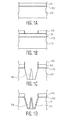
- a method of manufacturing a trench in a semiconductor device is shown.
- a layer stack is formed on the surface of a semiconductor substrate 101, such as a silicon substrate.
- the layer stack includes a silicon oxide layer 102 on the surface of the semiconductor substrate 101 and a silicon nitride layer 104 on top of the silicon oxide layer 102.
- the silicon oxide layer 102 is formed, for example, by thermally oxidizing the semiconductor substrate 101.
- the silicon nitride layer 104 is then deposited on top of the silicon oxide layer 102 by chemical vapor deposition (CVD) or another deposition technique.
- a resist 106 is formed on top of the silicon nitride layer 104 and a pattern transfer is performed in the resist 106, as shown in Fig. 1B .
- the patterning process can be performed using a positive resist or a negative resist using any suitable patterning technique, such as photolithography through a mask.
- the pattern defines an isolation region where a shallow trench isolation will be formed, as will be described in more detail below.
- a trench is formed within the isolation region defined by the patterned resist.
- the trench is etched by dry etching using the resist 106 and the patterned silicon nitride layer 104 as a mask. The dry etching removes the part of the silicon oxide layer 102 in the isolation region, and creates a recess in the top surface of the semiconductor substrate 101 in the isolation region.
- the etch process is blocked, for example by a particle on the surface of the semiconductor substrate 101, thereby forming a needle defect 108 beneath the particle blocking the etch process.
- the trench formation can also produce any other type of unwanted defect, such as a pillar defect or cone defect.
- the term needle defect is used in the following descriptions of the embodiments, but the embodiments are not limited to needle defects and can also be applied to any other defects occurring during the formation of trenches in semiconductor devices.
- the needle defect 108 is protruding from the bottom surface of the trench, as shown in Fig. 1C .
- the needle defect is protruding from the sidewalls of the trench. More than one defect may also be formed.
- the height of the needle defect 108 as shown in Fig. 1C is approximately the same height as the depth of the recess within the semiconductor substrate 101. In other words, the top of the needle defect 108 is near the level of the top surface of the semiconductor substrate 101. However, the embodiments are not limited to this height.
- a liner oxide 110 is formed within the isolation region.
- a thermal oxidation process can be used to form the liner oxide 110.
- the liner oxide 110 is formed at the surface of the sidewalls of the trench, at the bottom of the trench, and over the surface of the needle defect 108.
- the thickness of the liner oxide 110 is about 25nm.
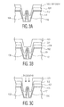
- a high density plasma (HDP) oxide 202 is formed on top of the semiconductor device, covering the patterned silicon nitride layer 106 and partially filling the trench.
- the process step shown in Fig. 2A follows the process step as described with reference to Fig. 1D above.
- the step of forming a liner oxide as described in Fig. 1D may be skipped and the HDP oxide 202 may be directly formed in the trench on top of and in contact with the semiconductor substrate 101.
- the trench is only partially filled with the HDP oxide 202 and the thickness of the deposited HDP oxide 202 over the top of the needle defect 108 is much smaller than the thickness of the deposited HDP oxide 202 over the bottom and sidewalls of the trench.
- the HDP oxide deposition uses conditions that yield a 2.5K HDP, which produces a film of HDP oxide with a thickness of about 2500 angstrom (250nm) on large flat surfaces such as the silicon nitride layer 104.
- the thickness of the HDP oxide 202 deposited over the bottom and sidewalls of the trench is also on the order of 250nm, whereas the thickness of the HDP oxide 202 deposited over the upper parts of the sidewalls of the needle defect 108 and over the top of the needle defect is much smaller and can be on the order of 25nm or less.
- the thickness of the deposited HDP oxide 202 diminishes radially towards the central vertical axis of the needle defect 108.
- an oxide etch is applied to remove the parts of the HDP oxide 202 and liner oxide 110 covering the top of the needle defect 108, thereby exposing the top of the needle defect, whereas the sidewalls and the bottom of the trench are still covered by the liner oxide 110 and the HDP oxide 202.
- the oxide etch can be a dry etch or a wet etch, such as reactive ion etching, chemical dry etching, buffered oxide etch, or any other suitable technique used to etch oxide films.
- the oxide etch uses parameters to remove a thickness of oxide equal to the combined thickness of the liner oxide 110 and HDP oxide 202 over the top of the needle defect 108.
- an oxide etch resulting in a 50nm oxide removal can be used to expose the top of the needle defect while leaving the bottom and sidewalls of the trench covered in HDP oxide.
- a polysilicon or silicon etch is applied to reduce the height of the needle defect 108.
- the polysilicon or silicon etch can be a dry etch or a wet etch using any suitable technique to remove at least parts of the needle defect 108. Because the top of the needle defect 108 is exposed, the polysilicon or silicon etch reaches the top of the needle defect and etches back the needle defect beginning from the top and progressing towards the bottom during the etching process.
- the polysilicon or silicon etch is highly selective to silicon oxide and therefore selectively etches back the needle defect 108 while leaving the HDP oxide 202 intact.
- the height of the needle defect 108 is reduced after the polysilicon or silicon etch as compared to the height of the needle defect before the etching process.
- the polysilicon or silicon etch does not attack the trench, and thus the sidewalls of the trench are not affected by the polysilicon or silicon etch.
- Examples of a polysilicon or silicon etch use parameters to reduce the height of the needle defect 108 by about 300nm.
- a further HDP oxide 204 is deposited over the semiconductor device to fill the remainder of the trench.
- the deposition of the HDP oxide 204 leaves a small air gap between the HDP oxide 204 and the needle defect 108, as shown in Fig. 2D .
- the HDP oxide 204 is in direct contact with the needle defect 108.
- a chemical mechanical planarization (CMP) can then be performed such that the silicon nitride layer 104 is exposed, as shown in Fig. 2E .
- the silicon nitride layer 104 may then be removed to form the shallow trench isolation region as shown in Fig. 2F .
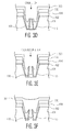
- a high density plasma (HDP) oxide 302 is formed on top of the semiconductor device, similar to the process step described above with reference to Fig. 2A .
- the process step shown in Fig. 3A follows the process step as described with reference to Fig. 1D above.
- the HDP oxide 302 covers the remaining silicon nitride layer 104 and partially fills the trench.
- the thickness of the HDP oxide 302 on the sidewalls of the trench may be smaller than the thickness of the HDP oxide at the bottom of the trench. Further, only a very thin layer of HDP oxide 302 is deposited over the top of the needle defect 108. In order to protect the sidewalls of the trench from being etched further during subsequent process steps, the subsequent etching of the needle defect 108 can be done in a masked way, as described in more detail below with reference to Figs. 3B-3F .
- a resist 303 such as a photoresist is formed over the trench.
- the resist 303 is patterned to remove the part of the resist 303 that is above the needle defect, as shown in Fig. 3C .
- Patterning of the resist may be done, for example, in a masked way using a photomask and photolithography, or may be done without a mask.
- patterning of the resist 303 is done in such a way that the sidewalls of the trench are still at least partially covered by the resist 303, while the HDP oxide 302 above the top of the needle defect is exposed.
- the patterned resist 303 then acts as a mask subsequent etching steps, as described below with reference to Figs. 3D and 3E .
- an oxide etch is applied to remove the HDP oxide 302 and liner oxide 110 covering the top of the needle defect 108, thereby exposing the top of the needle defect.
- the sidewalls of the trench are protected by the resist 303, thereby preventing the oxide etch from etching through the HDP oxide 302 and liner oxide 110 above the sidewalls and into the semiconductor substrate 101.
- a polysilicon or silicon etch is applied to reduce the height of the needle defect 108. Because the top of the needle defect 108 is exposed, the polysilicon or silicon etch reaches the top of the needle defect and etches back and reduces the height of the needle defect. Because of the protective properties of the HDP oxide 302 and the resist 303, the polysilicon or silicon etch does not affect the trench of the trench isolation region and does not affect the rest of the processing steps.
- a further HDP oxide 304 is deposited over the semiconductor device to fill the remainder of the trench to form a shallow trench isolation region as shown in Fig. 3F .
- the HDP oxide 304 is directly deposited over the needle defect 108 and is in contact with the needle defect.
- the deposition of the HDP oxide 304 creates a small void between the HDP oxide 304 and the needle defect 108.
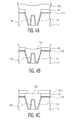
- a high density plasma (HDP) oxide 402 is formed on top of the semiconductor device.
- the process step shown in Fig. 4A follows the process step as described with reference to Fig. 1D above.
- the HDP oxide 302 covers the remaining silicon nitride layer 104 and fully fills the trench to form a shallow trench isolation.
- a chemical mechanical planarization is performed on the surface of the semiconductor device.
- CMP chemical mechanical planarization
- a resist 403 such as a photoresist is formed over the trench.
- the resist 403 is patterned to remove the part of the resist 403 that is above the needle defect while leaving the resist 403 above the sidewalls of the trench, as shown in Fig. 4C .
- Patterning of the resist may be done, for example, in a masked way using photolithography.
- an oxide etch is applied to remove the HDP oxide 402 and liner oxide 110 covering the top of the needle defect 108, thereby exposing the top of the needle defect.
- the patterned resist 403 acts as a mask subsequent etching steps. During the oxide etch, the sidewalls of the trench are protected by the resist 403, thereby preventing the oxide etch from etching through the HDP oxide 402 and liner oxide 110 above the sidewalls and into the semiconductor substrate 101.
- a silicon etch is applied to reduce the height of the needle defect 108. Because of the protective properties of the HDP oxide 402 and the resist 403, the silicon etch does not affect the shape of the trench of the shallow trench isolation region. In subsequent processing steps, the trench may be filled with a further HDP oxide and a further CMP may be performed to produce a shallow trench isolation with a reduced needle defect.
Applications Claiming Priority (1)
| Application Number | Priority Date | Filing Date | Title |
|---|---|---|---|
| US14/254,523 US9105687B1 (en) | 2014-04-16 | 2014-04-16 | Method for reducing defects in shallow trench isolation |
Publications (2)
| Publication Number | Publication Date |
|---|---|
| EP2933829A1 true EP2933829A1 (de) | 2015-10-21 |
| EP2933829B1 EP2933829B1 (de) | 2019-08-14 |
Family
ID=53015517
Family Applications (1)
| Application Number | Title | Priority Date | Filing Date |
|---|---|---|---|
| EP15163578.6A Active EP2933829B1 (de) | 2014-04-16 | 2015-04-14 | Verfahren zur reduzierung der defekte in grabenisolation |
Country Status (3)
| Country | Link |
|---|---|
| US (1) | US9105687B1 (de) |
| EP (1) | EP2933829B1 (de) |
| CN (1) | CN105006447B (de) |
Families Citing this family (5)
| Publication number | Priority date | Publication date | Assignee | Title |
|---|---|---|---|---|
| US9953861B2 (en) | 2014-11-26 | 2018-04-24 | Taiwan Semiconductor Manufacturing Company, Ltd. | Semiconductor device having a shallow trench isolation structure and methods of forming the same |
| US10825717B1 (en) * | 2019-07-09 | 2020-11-03 | Nxp B.V. | Method for making high voltage transistors insensitive to needle defects in shallow trench isolation |
| CN112366131B (zh) * | 2020-10-21 | 2023-01-03 | 武汉新芯集成电路制造有限公司 | 一种半导体器件的制造方法 |
| TWI783413B (zh) * | 2021-03-19 | 2022-11-11 | 世界先進積體電路股份有限公司 | 半導體裝置的形成方法 |
| US11569121B2 (en) * | 2021-05-26 | 2023-01-31 | Vanguard International Semiconductor Corporation | Methods for forming semiconductor devices |
Citations (2)
| Publication number | Priority date | Publication date | Assignee | Title |
|---|---|---|---|---|
| US20050139951A1 (en) * | 2003-12-29 | 2005-06-30 | Hynix Semiconductor Inc. | Semiconducotor device and method for isolating the same |
| US20130164907A1 (en) * | 2011-12-22 | 2013-06-27 | Samsung Electronics Co., Ltd. | Methods of forming a thin film and methods of fabricating a semiconductor device including using the same |
Family Cites Families (8)
| Publication number | Priority date | Publication date | Assignee | Title |
|---|---|---|---|---|
| US5795684A (en) * | 1996-04-05 | 1998-08-18 | Intel Corporation | Photolithography mask and method of fabrication |
| US5747377A (en) | 1996-09-06 | 1998-05-05 | Powerchip Semiconductor Corp. | Process for forming shallow trench isolation |
| JP3858462B2 (ja) | 1998-07-30 | 2006-12-13 | 株式会社日立製作所 | 半導体装置の製造方法 |
| US6825544B1 (en) * | 1998-12-09 | 2004-11-30 | Cypress Semiconductor Corporation | Method for shallow trench isolation and shallow trench isolation structure |
| US6194284B1 (en) * | 1999-08-30 | 2001-02-27 | Taiwan Semiconductor Manufacturing Company | Method for forming residue free etched silicon layer |
| TW586181B (en) | 2002-12-25 | 2004-05-01 | Macronix Int Co Ltd | Method of fabricating shallow trench isolation |
| JP4825402B2 (ja) | 2004-01-14 | 2011-11-30 | ルネサスエレクトロニクス株式会社 | 半導体装置の製造方法 |
| CN102044429B (zh) * | 2009-10-23 | 2012-10-31 | 北京北方微电子基地设备工艺研究中心有限责任公司 | 一种硅片的刻蚀方法 |
-
2014
- 2014-04-16 US US14/254,523 patent/US9105687B1/en active Active
-
2015
- 2015-03-09 CN CN201510102964.1A patent/CN105006447B/zh active Active
- 2015-04-14 EP EP15163578.6A patent/EP2933829B1/de active Active
Patent Citations (2)
| Publication number | Priority date | Publication date | Assignee | Title |
|---|---|---|---|---|
| US20050139951A1 (en) * | 2003-12-29 | 2005-06-30 | Hynix Semiconductor Inc. | Semiconducotor device and method for isolating the same |
| US20130164907A1 (en) * | 2011-12-22 | 2013-06-27 | Samsung Electronics Co., Ltd. | Methods of forming a thin film and methods of fabricating a semiconductor device including using the same |
Also Published As
| Publication number | Publication date |
|---|---|
| CN105006447A (zh) | 2015-10-28 |
| US9105687B1 (en) | 2015-08-11 |
| CN105006447B (zh) | 2018-04-10 |
| EP2933829B1 (de) | 2019-08-14 |
Similar Documents
| Publication | Publication Date | Title |
|---|---|---|
| EP2933829B1 (de) | Verfahren zur reduzierung der defekte in grabenisolation | |
| TWI389312B (zh) | 溝渠式金屬氧化物半導體 | |
| KR102374206B1 (ko) | 반도체 장치 제조 방법 | |
| WO2010030468A1 (en) | Self-aligned trench formation | |
| US8673734B2 (en) | Semiconductor device and method for fabricating the same | |
| KR101917029B1 (ko) | 랩-어라운드 컨택트 집적 스킴 | |
| CN108666263B (zh) | 接触孔的制造方法 | |
| US8088664B2 (en) | Method of manufacturing integrated deep and shallow trench isolation structures | |
| JP2011216651A (ja) | 半導体装置の製造方法 | |
| TWI467665B (zh) | 結構元件製造方法及具結構元件之半導體裝置 | |
| JP2014078715A (ja) | Utbbに関するコンタクト関連短絡に対して保護する方法 | |
| US9437674B2 (en) | Insulating trench forming method | |
| CN110233097B (zh) | 半导体器件的形成方法 | |
| US6391739B1 (en) | Process of eliminating a shallow trench isolation divot | |
| TWI732256B (zh) | 半導體結構及其製造方法 | |
| TW202113940A (zh) | Gaa電晶體中藉由選擇性頂部沉積製程之底部隔離形成方法 | |
| US20200144111A1 (en) | Metal interconnection structure and method for fabricating same | |
| US9875909B1 (en) | Method for planarizing material layer | |
| KR100886004B1 (ko) | 반도체 소자 제조 방법 | |
| TWI715967B (zh) | 半導體結構及其製造方法 | |
| WO2022099786A1 (zh) | 半导体功率器件的制造方法 | |
| US20240038838A1 (en) | Semiconductor structure and method for fabricating same | |
| US20230402288A1 (en) | Method of removing step height on gate structure | |
| CN111384151B (zh) | 半导体基底及其制备方法 | |
| KR20010008607A (ko) | 반도체장치의 소자분리막 형성방법 |
Legal Events
| Date | Code | Title | Description |
|---|---|---|---|
| PUAI | Public reference made under article 153(3) epc to a published international application that has entered the european phase |
Free format text: ORIGINAL CODE: 0009012 |
|
| AK | Designated contracting states |
Kind code of ref document: A1 Designated state(s): AL AT BE BG CH CY CZ DE DK EE ES FI FR GB GR HR HU IE IS IT LI LT LU LV MC MK MT NL NO PL PT RO RS SE SI SK SM TR |
|
| AX | Request for extension of the european patent |
Extension state: BA ME |
|
| 17P | Request for examination filed |
Effective date: 20160421 |
|
| RBV | Designated contracting states (corrected) |
Designated state(s): AL AT BE BG CH CY CZ DE DK EE ES FI FR GB GR HR HU IE IS IT LI LT LU LV MC MK MT NL NO PL PT RO RS SE SI SK SM TR |
|
| GRAP | Despatch of communication of intention to grant a patent |
Free format text: ORIGINAL CODE: EPIDOSNIGR1 |
|
| STAA | Information on the status of an ep patent application or granted ep patent |
Free format text: STATUS: GRANT OF PATENT IS INTENDED |
|
| RIC1 | Information provided on ipc code assigned before grant |
Ipc: H01L 21/306 20060101ALI20190327BHEP Ipc: H01L 21/3065 20060101ALI20190327BHEP Ipc: H01L 21/764 20060101ALI20190327BHEP Ipc: H01L 21/762 20060101AFI20190327BHEP |
|
| INTG | Intention to grant announced |
Effective date: 20190417 |
|
| GRAS | Grant fee paid |
Free format text: ORIGINAL CODE: EPIDOSNIGR3 |
|
| GRAA | (expected) grant |
Free format text: ORIGINAL CODE: 0009210 |
|
| STAA | Information on the status of an ep patent application or granted ep patent |
Free format text: STATUS: THE PATENT HAS BEEN GRANTED |
|
| AK | Designated contracting states |
Kind code of ref document: B1 Designated state(s): AL AT BE BG CH CY CZ DE DK EE ES FI FR GB GR HR HU IE IS IT LI LT LU LV MC MK MT NL NO PL PT RO RS SE SI SK SM TR |
|
| REG | Reference to a national code |
Ref country code: GB Ref legal event code: FG4D |
|
| REG | Reference to a national code |
Ref country code: CH Ref legal event code: EP Ref country code: AT Ref legal event code: REF Ref document number: 1168027 Country of ref document: AT Kind code of ref document: T Effective date: 20190815 |
|
| REG | Reference to a national code |
Ref country code: IE Ref legal event code: FG4D |
|
| REG | Reference to a national code |
Ref country code: DE Ref legal event code: R096 Ref document number: 602015035679 Country of ref document: DE |
|
| REG | Reference to a national code |
Ref country code: NL Ref legal event code: MP Effective date: 20190814 |
|
| REG | Reference to a national code |
Ref country code: LT Ref legal event code: MG4D |
|
| PG25 | Lapsed in a contracting state [announced via postgrant information from national office to epo] |
Ref country code: PT Free format text: LAPSE BECAUSE OF FAILURE TO SUBMIT A TRANSLATION OF THE DESCRIPTION OR TO PAY THE FEE WITHIN THE PRESCRIBED TIME-LIMIT Effective date: 20191216 Ref country code: NO Free format text: LAPSE BECAUSE OF FAILURE TO SUBMIT A TRANSLATION OF THE DESCRIPTION OR TO PAY THE FEE WITHIN THE PRESCRIBED TIME-LIMIT Effective date: 20191114 Ref country code: SE Free format text: LAPSE BECAUSE OF FAILURE TO SUBMIT A TRANSLATION OF THE DESCRIPTION OR TO PAY THE FEE WITHIN THE PRESCRIBED TIME-LIMIT Effective date: 20190814 Ref country code: FI Free format text: LAPSE BECAUSE OF FAILURE TO SUBMIT A TRANSLATION OF THE DESCRIPTION OR TO PAY THE FEE WITHIN THE PRESCRIBED TIME-LIMIT Effective date: 20190814 Ref country code: NL Free format text: LAPSE BECAUSE OF FAILURE TO SUBMIT A TRANSLATION OF THE DESCRIPTION OR TO PAY THE FEE WITHIN THE PRESCRIBED TIME-LIMIT Effective date: 20190814 Ref country code: HR Free format text: LAPSE BECAUSE OF FAILURE TO SUBMIT A TRANSLATION OF THE DESCRIPTION OR TO PAY THE FEE WITHIN THE PRESCRIBED TIME-LIMIT Effective date: 20190814 Ref country code: BG Free format text: LAPSE BECAUSE OF FAILURE TO SUBMIT A TRANSLATION OF THE DESCRIPTION OR TO PAY THE FEE WITHIN THE PRESCRIBED TIME-LIMIT Effective date: 20191114 Ref country code: LT Free format text: LAPSE BECAUSE OF FAILURE TO SUBMIT A TRANSLATION OF THE DESCRIPTION OR TO PAY THE FEE WITHIN THE PRESCRIBED TIME-LIMIT Effective date: 20190814 |
|
| REG | Reference to a national code |
Ref country code: AT Ref legal event code: MK05 Ref document number: 1168027 Country of ref document: AT Kind code of ref document: T Effective date: 20190814 |
|
| PG25 | Lapsed in a contracting state [announced via postgrant information from national office to epo] |
Ref country code: AL Free format text: LAPSE BECAUSE OF FAILURE TO SUBMIT A TRANSLATION OF THE DESCRIPTION OR TO PAY THE FEE WITHIN THE PRESCRIBED TIME-LIMIT Effective date: 20190814 Ref country code: GR Free format text: LAPSE BECAUSE OF FAILURE TO SUBMIT A TRANSLATION OF THE DESCRIPTION OR TO PAY THE FEE WITHIN THE PRESCRIBED TIME-LIMIT Effective date: 20191115 Ref country code: ES Free format text: LAPSE BECAUSE OF FAILURE TO SUBMIT A TRANSLATION OF THE DESCRIPTION OR TO PAY THE FEE WITHIN THE PRESCRIBED TIME-LIMIT Effective date: 20190814 Ref country code: LV Free format text: LAPSE BECAUSE OF FAILURE TO SUBMIT A TRANSLATION OF THE DESCRIPTION OR TO PAY THE FEE WITHIN THE PRESCRIBED TIME-LIMIT Effective date: 20190814 Ref country code: RS Free format text: LAPSE BECAUSE OF FAILURE TO SUBMIT A TRANSLATION OF THE DESCRIPTION OR TO PAY THE FEE WITHIN THE PRESCRIBED TIME-LIMIT Effective date: 20190814 Ref country code: IS Free format text: LAPSE BECAUSE OF FAILURE TO SUBMIT A TRANSLATION OF THE DESCRIPTION OR TO PAY THE FEE WITHIN THE PRESCRIBED TIME-LIMIT Effective date: 20191214 |
|
| PG25 | Lapsed in a contracting state [announced via postgrant information from national office to epo] |
Ref country code: TR Free format text: LAPSE BECAUSE OF FAILURE TO SUBMIT A TRANSLATION OF THE DESCRIPTION OR TO PAY THE FEE WITHIN THE PRESCRIBED TIME-LIMIT Effective date: 20190814 |
|
| PG25 | Lapsed in a contracting state [announced via postgrant information from national office to epo] |
Ref country code: RO Free format text: LAPSE BECAUSE OF FAILURE TO SUBMIT A TRANSLATION OF THE DESCRIPTION OR TO PAY THE FEE WITHIN THE PRESCRIBED TIME-LIMIT Effective date: 20190814 Ref country code: EE Free format text: LAPSE BECAUSE OF FAILURE TO SUBMIT A TRANSLATION OF THE DESCRIPTION OR TO PAY THE FEE WITHIN THE PRESCRIBED TIME-LIMIT Effective date: 20190814 Ref country code: PL Free format text: LAPSE BECAUSE OF FAILURE TO SUBMIT A TRANSLATION OF THE DESCRIPTION OR TO PAY THE FEE WITHIN THE PRESCRIBED TIME-LIMIT Effective date: 20190814 Ref country code: DK Free format text: LAPSE BECAUSE OF FAILURE TO SUBMIT A TRANSLATION OF THE DESCRIPTION OR TO PAY THE FEE WITHIN THE PRESCRIBED TIME-LIMIT Effective date: 20190814 Ref country code: IT Free format text: LAPSE BECAUSE OF FAILURE TO SUBMIT A TRANSLATION OF THE DESCRIPTION OR TO PAY THE FEE WITHIN THE PRESCRIBED TIME-LIMIT Effective date: 20190814 Ref country code: AT Free format text: LAPSE BECAUSE OF FAILURE TO SUBMIT A TRANSLATION OF THE DESCRIPTION OR TO PAY THE FEE WITHIN THE PRESCRIBED TIME-LIMIT Effective date: 20190814 |
|
| PG25 | Lapsed in a contracting state [announced via postgrant information from national office to epo] |
Ref country code: IS Free format text: LAPSE BECAUSE OF FAILURE TO SUBMIT A TRANSLATION OF THE DESCRIPTION OR TO PAY THE FEE WITHIN THE PRESCRIBED TIME-LIMIT Effective date: 20200224 Ref country code: CZ Free format text: LAPSE BECAUSE OF FAILURE TO SUBMIT A TRANSLATION OF THE DESCRIPTION OR TO PAY THE FEE WITHIN THE PRESCRIBED TIME-LIMIT Effective date: 20190814 Ref country code: SM Free format text: LAPSE BECAUSE OF FAILURE TO SUBMIT A TRANSLATION OF THE DESCRIPTION OR TO PAY THE FEE WITHIN THE PRESCRIBED TIME-LIMIT Effective date: 20190814 Ref country code: SK Free format text: LAPSE BECAUSE OF FAILURE TO SUBMIT A TRANSLATION OF THE DESCRIPTION OR TO PAY THE FEE WITHIN THE PRESCRIBED TIME-LIMIT Effective date: 20190814 |
|
| REG | Reference to a national code |
Ref country code: DE Ref legal event code: R097 Ref document number: 602015035679 Country of ref document: DE |
|
| PLBE | No opposition filed within time limit |
Free format text: ORIGINAL CODE: 0009261 |
|
| STAA | Information on the status of an ep patent application or granted ep patent |
Free format text: STATUS: NO OPPOSITION FILED WITHIN TIME LIMIT |
|
| PG2D | Information on lapse in contracting state deleted |
Ref country code: IS |
|
| 26N | No opposition filed |
Effective date: 20200603 |
|
| PG25 | Lapsed in a contracting state [announced via postgrant information from national office to epo] |
Ref country code: SI Free format text: LAPSE BECAUSE OF FAILURE TO SUBMIT A TRANSLATION OF THE DESCRIPTION OR TO PAY THE FEE WITHIN THE PRESCRIBED TIME-LIMIT Effective date: 20190814 |
|
| PG25 | Lapsed in a contracting state [announced via postgrant information from national office to epo] |
Ref country code: MC Free format text: LAPSE BECAUSE OF FAILURE TO SUBMIT A TRANSLATION OF THE DESCRIPTION OR TO PAY THE FEE WITHIN THE PRESCRIBED TIME-LIMIT Effective date: 20190814 |
|
| REG | Reference to a national code |
Ref country code: CH Ref legal event code: PL |
|
| PG25 | Lapsed in a contracting state [announced via postgrant information from national office to epo] |
Ref country code: CH Free format text: LAPSE BECAUSE OF NON-PAYMENT OF DUE FEES Effective date: 20200430 Ref country code: LU Free format text: LAPSE BECAUSE OF NON-PAYMENT OF DUE FEES Effective date: 20200414 Ref country code: LI Free format text: LAPSE BECAUSE OF NON-PAYMENT OF DUE FEES Effective date: 20200430 |
|
| REG | Reference to a national code |
Ref country code: BE Ref legal event code: MM Effective date: 20200430 |
|
| PG25 | Lapsed in a contracting state [announced via postgrant information from national office to epo] |
Ref country code: BE Free format text: LAPSE BECAUSE OF NON-PAYMENT OF DUE FEES Effective date: 20200430 |
|
| GBPC | Gb: european patent ceased through non-payment of renewal fee |
Effective date: 20200414 |
|
| PG25 | Lapsed in a contracting state [announced via postgrant information from national office to epo] |
Ref country code: IE Free format text: LAPSE BECAUSE OF NON-PAYMENT OF DUE FEES Effective date: 20200414 Ref country code: GB Free format text: LAPSE BECAUSE OF NON-PAYMENT OF DUE FEES Effective date: 20200414 |
|
| PG25 | Lapsed in a contracting state [announced via postgrant information from national office to epo] |
Ref country code: MT Free format text: LAPSE BECAUSE OF FAILURE TO SUBMIT A TRANSLATION OF THE DESCRIPTION OR TO PAY THE FEE WITHIN THE PRESCRIBED TIME-LIMIT Effective date: 20190814 Ref country code: CY Free format text: LAPSE BECAUSE OF FAILURE TO SUBMIT A TRANSLATION OF THE DESCRIPTION OR TO PAY THE FEE WITHIN THE PRESCRIBED TIME-LIMIT Effective date: 20190814 |
|
| PG25 | Lapsed in a contracting state [announced via postgrant information from national office to epo] |
Ref country code: MK Free format text: LAPSE BECAUSE OF FAILURE TO SUBMIT A TRANSLATION OF THE DESCRIPTION OR TO PAY THE FEE WITHIN THE PRESCRIBED TIME-LIMIT Effective date: 20190814 |
|
| PGFP | Annual fee paid to national office [announced via postgrant information from national office to epo] |
Ref country code: FR Payment date: 20230321 Year of fee payment: 9 |
|
| PGFP | Annual fee paid to national office [announced via postgrant information from national office to epo] |
Ref country code: DE Payment date: 20230321 Year of fee payment: 9 |
|
| P01 | Opt-out of the competence of the unified patent court (upc) registered |
Effective date: 20230725 |