EP2908338A1 - Semiconductor device - Google Patents
Semiconductor device Download PDFInfo
- Publication number
- EP2908338A1 EP2908338A1 EP13846815.2A EP13846815A EP2908338A1 EP 2908338 A1 EP2908338 A1 EP 2908338A1 EP 13846815 A EP13846815 A EP 13846815A EP 2908338 A1 EP2908338 A1 EP 2908338A1
- Authority
- EP
- European Patent Office
- Prior art keywords
- pattern
- circuit board
- printed circuit
- conductive pattern
- conductive
- Prior art date
- Legal status (The legal status is an assumption and is not a legal conclusion. Google has not performed a legal analysis and makes no representation as to the accuracy of the status listed.)
- Withdrawn
Links
Images





Classifications
-
- H—ELECTRICITY
- H05—ELECTRIC TECHNIQUES NOT OTHERWISE PROVIDED FOR
- H05K—PRINTED CIRCUITS; CASINGS OR CONSTRUCTIONAL DETAILS OF ELECTRIC APPARATUS; MANUFACTURE OF ASSEMBLAGES OF ELECTRICAL COMPONENTS
- H05K1/00—Printed circuits
- H05K1/18—Printed circuits structurally associated with non-printed electric components
- H05K1/181—Printed circuits structurally associated with non-printed electric components associated with surface mounted components
-
- H—ELECTRICITY
- H05—ELECTRIC TECHNIQUES NOT OTHERWISE PROVIDED FOR
- H05K—PRINTED CIRCUITS; CASINGS OR CONSTRUCTIONAL DETAILS OF ELECTRIC APPARATUS; MANUFACTURE OF ASSEMBLAGES OF ELECTRICAL COMPONENTS
- H05K1/00—Printed circuits
- H05K1/02—Details
- H05K1/0201—Thermal arrangements, e.g. for cooling, heating or preventing overheating
- H05K1/0212—Printed circuits or mounted components having integral heating means
-
- H—ELECTRICITY
- H05—ELECTRIC TECHNIQUES NOT OTHERWISE PROVIDED FOR
- H05K—PRINTED CIRCUITS; CASINGS OR CONSTRUCTIONAL DETAILS OF ELECTRIC APPARATUS; MANUFACTURE OF ASSEMBLAGES OF ELECTRICAL COMPONENTS
- H05K1/00—Printed circuits
- H05K1/02—Details
- H05K1/0296—Conductive pattern lay-out details not covered by sub groups H05K1/02 - H05K1/0295
-
- H—ELECTRICITY
- H05—ELECTRIC TECHNIQUES NOT OTHERWISE PROVIDED FOR
- H05K—PRINTED CIRCUITS; CASINGS OR CONSTRUCTIONAL DETAILS OF ELECTRIC APPARATUS; MANUFACTURE OF ASSEMBLAGES OF ELECTRICAL COMPONENTS
- H05K3/00—Apparatus or processes for manufacturing printed circuits
- H05K3/30—Assembling printed circuits with electric components, e.g. with resistors
- H05K3/32—Assembling printed circuits with electric components, e.g. with resistors electrically connecting electric components or wires to printed circuits
- H05K3/34—Assembling printed circuits with electric components, e.g. with resistors electrically connecting electric components or wires to printed circuits by soldering
- H05K3/3447—Lead-in-hole components
-
- H—ELECTRICITY
- H05—ELECTRIC TECHNIQUES NOT OTHERWISE PROVIDED FOR
- H05K—PRINTED CIRCUITS; CASINGS OR CONSTRUCTIONAL DETAILS OF ELECTRIC APPARATUS; MANUFACTURE OF ASSEMBLAGES OF ELECTRICAL COMPONENTS
- H05K7/00—Constructional details common to different types of electric apparatus
- H05K7/20—Modifications to facilitate cooling, ventilating, or heating
- H05K7/2089—Modifications to facilitate cooling, ventilating, or heating for power electronics, e.g. for inverters for controlling motor
-
- H—ELECTRICITY
- H10—SEMICONDUCTOR DEVICES; ELECTRIC SOLID-STATE DEVICES NOT OTHERWISE PROVIDED FOR
- H10W—GENERIC PACKAGES, INTERCONNECTIONS, CONNECTORS OR OTHER CONSTRUCTIONAL DETAILS OF DEVICES COVERED BY CLASS H10
- H10W40/00—Arrangements for thermal protection or thermal control
- H10W40/20—Arrangements for cooling
- H10W40/25—Arrangements for cooling characterised by their materials
- H10W40/255—Arrangements for cooling characterised by their materials having a laminate or multilayered structure, e.g. direct bond copper [DBC] ceramic substrates
-
- H—ELECTRICITY
- H10—SEMICONDUCTOR DEVICES; ELECTRIC SOLID-STATE DEVICES NOT OTHERWISE PROVIDED FOR
- H10W—GENERIC PACKAGES, INTERCONNECTIONS, CONNECTORS OR OTHER CONSTRUCTIONAL DETAILS OF DEVICES COVERED BY CLASS H10
- H10W72/00—Interconnections or connectors in packages
- H10W72/20—Bump connectors, e.g. solder bumps or copper pillars; Dummy bumps; Thermal bumps
-
- H—ELECTRICITY
- H10—SEMICONDUCTOR DEVICES; ELECTRIC SOLID-STATE DEVICES NOT OTHERWISE PROVIDED FOR
- H10W—GENERIC PACKAGES, INTERCONNECTIONS, CONNECTORS OR OTHER CONSTRUCTIONAL DETAILS OF DEVICES COVERED BY CLASS H10
- H10W74/00—Encapsulations, e.g. protective coatings
- H10W74/10—Encapsulations, e.g. protective coatings characterised by their shape or disposition
- H10W74/111—Encapsulations, e.g. protective coatings characterised by their shape or disposition the semiconductor body being completely enclosed
-
- H—ELECTRICITY
- H10—SEMICONDUCTOR DEVICES; ELECTRIC SOLID-STATE DEVICES NOT OTHERWISE PROVIDED FOR
- H10W—GENERIC PACKAGES, INTERCONNECTIONS, CONNECTORS OR OTHER CONSTRUCTIONAL DETAILS OF DEVICES COVERED BY CLASS H10
- H10W76/00—Containers; Fillings or auxiliary members therefor; Seals
- H10W76/10—Containers or parts thereof
- H10W76/12—Containers or parts thereof characterised by their shape
-
- H—ELECTRICITY
- H10—SEMICONDUCTOR DEVICES; ELECTRIC SOLID-STATE DEVICES NOT OTHERWISE PROVIDED FOR
- H10W—GENERIC PACKAGES, INTERCONNECTIONS, CONNECTORS OR OTHER CONSTRUCTIONAL DETAILS OF DEVICES COVERED BY CLASS H10
- H10W90/00—Package configurations
-
- H—ELECTRICITY
- H10—SEMICONDUCTOR DEVICES; ELECTRIC SOLID-STATE DEVICES NOT OTHERWISE PROVIDED FOR
- H10W—GENERIC PACKAGES, INTERCONNECTIONS, CONNECTORS OR OTHER CONSTRUCTIONAL DETAILS OF DEVICES COVERED BY CLASS H10
- H10W90/00—Package configurations
- H10W90/401—Package configurations characterised by multiple insulating or insulated package substrates, interposers or RDLs
-
- H—ELECTRICITY
- H05—ELECTRIC TECHNIQUES NOT OTHERWISE PROVIDED FOR
- H05K—PRINTED CIRCUITS; CASINGS OR CONSTRUCTIONAL DETAILS OF ELECTRIC APPARATUS; MANUFACTURE OF ASSEMBLAGES OF ELECTRICAL COMPONENTS
- H05K1/00—Printed circuits
- H05K1/02—Details
- H05K1/0213—Electrical arrangements not otherwise provided for
- H05K1/0237—High frequency adaptations
- H05K1/0243—Printed circuits associated with mounted high frequency components
-
- H—ELECTRICITY
- H05—ELECTRIC TECHNIQUES NOT OTHERWISE PROVIDED FOR
- H05K—PRINTED CIRCUITS; CASINGS OR CONSTRUCTIONAL DETAILS OF ELECTRIC APPARATUS; MANUFACTURE OF ASSEMBLAGES OF ELECTRICAL COMPONENTS
- H05K2201/00—Indexing scheme relating to printed circuits covered by H05K1/00
- H05K2201/03—Conductive materials
- H05K2201/0332—Structure of the conductor
- H05K2201/0364—Conductor shape
-
- H—ELECTRICITY
- H05—ELECTRIC TECHNIQUES NOT OTHERWISE PROVIDED FOR
- H05K—PRINTED CIRCUITS; CASINGS OR CONSTRUCTIONAL DETAILS OF ELECTRIC APPARATUS; MANUFACTURE OF ASSEMBLAGES OF ELECTRICAL COMPONENTS
- H05K2201/00—Indexing scheme relating to printed circuits covered by H05K1/00
- H05K2201/06—Thermal details
-
- H—ELECTRICITY
- H05—ELECTRIC TECHNIQUES NOT OTHERWISE PROVIDED FOR
- H05K—PRINTED CIRCUITS; CASINGS OR CONSTRUCTIONAL DETAILS OF ELECTRIC APPARATUS; MANUFACTURE OF ASSEMBLAGES OF ELECTRICAL COMPONENTS
- H05K2201/00—Indexing scheme relating to printed circuits covered by H05K1/00
- H05K2201/09—Shape and layout
- H05K2201/09818—Shape or layout details not covered by a single group of H05K2201/09009 - H05K2201/09809
- H05K2201/09972—Partitioned, e.g. portions of a PCB dedicated to different functions; Boundary lines therefore; Portions of a PCB being processed separately or differently
-
- H—ELECTRICITY
- H10—SEMICONDUCTOR DEVICES; ELECTRIC SOLID-STATE DEVICES NOT OTHERWISE PROVIDED FOR
- H10W—GENERIC PACKAGES, INTERCONNECTIONS, CONNECTORS OR OTHER CONSTRUCTIONAL DETAILS OF DEVICES COVERED BY CLASS H10
- H10W72/00—Interconnections or connectors in packages
- H10W72/071—Connecting or disconnecting
- H10W72/073—Connecting or disconnecting of die-attach connectors
- H10W72/07331—Connecting techniques
- H10W72/07336—Soldering or alloying
-
- H—ELECTRICITY
- H10—SEMICONDUCTOR DEVICES; ELECTRIC SOLID-STATE DEVICES NOT OTHERWISE PROVIDED FOR
- H10W—GENERIC PACKAGES, INTERCONNECTIONS, CONNECTORS OR OTHER CONSTRUCTIONAL DETAILS OF DEVICES COVERED BY CLASS H10
- H10W72/00—Interconnections or connectors in packages
- H10W72/30—Die-attach connectors
- H10W72/351—Materials of die-attach connectors
- H10W72/352—Materials of die-attach connectors comprising metals or metalloids, e.g. solders
-
- H—ELECTRICITY
- H10—SEMICONDUCTOR DEVICES; ELECTRIC SOLID-STATE DEVICES NOT OTHERWISE PROVIDED FOR
- H10W—GENERIC PACKAGES, INTERCONNECTIONS, CONNECTORS OR OTHER CONSTRUCTIONAL DETAILS OF DEVICES COVERED BY CLASS H10
- H10W72/00—Interconnections or connectors in packages
- H10W72/851—Dispositions of multiple connectors or interconnections
- H10W72/874—On different surfaces
- H10W72/884—Die-attach connectors and bond wires
-
- H—ELECTRICITY
- H10—SEMICONDUCTOR DEVICES; ELECTRIC SOLID-STATE DEVICES NOT OTHERWISE PROVIDED FOR
- H10W—GENERIC PACKAGES, INTERCONNECTIONS, CONNECTORS OR OTHER CONSTRUCTIONAL DETAILS OF DEVICES COVERED BY CLASS H10
- H10W74/00—Encapsulations, e.g. protective coatings
-
- H—ELECTRICITY
- H10—SEMICONDUCTOR DEVICES; ELECTRIC SOLID-STATE DEVICES NOT OTHERWISE PROVIDED FOR
- H10W—GENERIC PACKAGES, INTERCONNECTIONS, CONNECTORS OR OTHER CONSTRUCTIONAL DETAILS OF DEVICES COVERED BY CLASS H10
- H10W74/00—Encapsulations, e.g. protective coatings
- H10W74/01—Manufacture or treatment
- H10W74/016—Manufacture or treatment using moulds
-
- H—ELECTRICITY
- H10—SEMICONDUCTOR DEVICES; ELECTRIC SOLID-STATE DEVICES NOT OTHERWISE PROVIDED FOR
- H10W—GENERIC PACKAGES, INTERCONNECTIONS, CONNECTORS OR OTHER CONSTRUCTIONAL DETAILS OF DEVICES COVERED BY CLASS H10
- H10W90/00—Package configurations
- H10W90/701—Package configurations characterised by the relative positions of pads or connectors relative to package parts
- H10W90/731—Package configurations characterised by the relative positions of pads or connectors relative to package parts of die-attach connectors
- H10W90/734—Package configurations characterised by the relative positions of pads or connectors relative to package parts of die-attach connectors between a chip and a stacked insulating package substrate, interposer or RDL
-
- H—ELECTRICITY
- H10—SEMICONDUCTOR DEVICES; ELECTRIC SOLID-STATE DEVICES NOT OTHERWISE PROVIDED FOR
- H10W—GENERIC PACKAGES, INTERCONNECTIONS, CONNECTORS OR OTHER CONSTRUCTIONAL DETAILS OF DEVICES COVERED BY CLASS H10
- H10W90/00—Package configurations
- H10W90/701—Package configurations characterised by the relative positions of pads or connectors relative to package parts
- H10W90/751—Package configurations characterised by the relative positions of pads or connectors relative to package parts of bond wires
- H10W90/753—Package configurations characterised by the relative positions of pads or connectors relative to package parts of bond wires between laterally-adjacent chips
-
- H—ELECTRICITY
- H10—SEMICONDUCTOR DEVICES; ELECTRIC SOLID-STATE DEVICES NOT OTHERWISE PROVIDED FOR
- H10W—GENERIC PACKAGES, INTERCONNECTIONS, CONNECTORS OR OTHER CONSTRUCTIONAL DETAILS OF DEVICES COVERED BY CLASS H10
- H10W90/00—Package configurations
- H10W90/701—Package configurations characterised by the relative positions of pads or connectors relative to package parts
- H10W90/751—Package configurations characterised by the relative positions of pads or connectors relative to package parts of bond wires
- H10W90/754—Package configurations characterised by the relative positions of pads or connectors relative to package parts of bond wires between a chip and a stacked insulating package substrate, interposer or RDL
Definitions
- the present invention relates to a semiconductor device in which is mounted a power semiconductor chip.
- a power semiconductor module is used in an inverter device configuring, for example, a power conversion device.
- the semiconductor device shown in, for example, Fig. 15 has been proposed as an existing semiconductor device.
- This existing semiconductor device is given as an example of, for example, a 2-in-1 semiconductor module 100.
- the semiconductor module 100 is such that a conductor patterned insulating substrate (ceramic insulating substrate) 102 is joined by a solder 103 onto a heat releasing metal base plate 101.
- the conductor patterned insulating substrate 102 has a ceramic substrate 102a, and is configured of a conductor pattern 102b bonded to the front surface of the ceramic substrate 102a and a back surface conductive film 102c bonded to the back surface of the ceramic substrate 102a.
- a semiconductor chip (semiconductor power chip) 104 is mounted across a solder 105 on the conductor pattern 102b of the conductor patterned insulating substrate 102.
- the metal base plate 101, conductor patterned insulating substrate 102, and semiconductor chip 104 are disposed inside a box-form resin case 106 of which the lower end is opened, and fixed inside the resin case 106 by injecting a resin sealing material.
- 107 is a metal bar terminal that forms an external lead-out terminal soldered to the conductor pattern 102b
- 108 is bonding wire that connects semiconductor chips 104, or the semiconductor chip 104 and the conductor pattern 102b.
- a power semiconductor module which is a power semiconductor module formed of a series connection circuit of a power semiconductor device (IGBT) and a diode (FWD) connected in anti-parallel thereto, wherein the inductance value inside the power semiconductor module is reduced to practically zero by an electrode bar connected to a first power supply potential output electrode or the like, an electrode bar connected to an additional electrode or the like, and an electrode bar connected to a second power supply potential output electrode or the like each being formed in plate form, and disposed across an insulator in close proximity to each other (for example, refer to PTL 2).
- IGBT power semiconductor device
- FWD diode
- a power semiconductor device wherein a rectangular ring-form wiring substrate is disposed on an upper portion of a bottom surface substrate so as to cover end and edge portions of the bottom surface substrate, a main collector electrode terminal and a main emitter electrode terminal are passed through an aperture portion in a central portion of the wiring substrate and caused to protrude from an aperture portion of a resin case, and a control emitter pad and gate pad are electrically connected via wires of equal length to a control emitter electrode and gate electrode (for example, refer to PTL 3).
- a semiconductor device including a semiconductor device unit in which is sealed a semiconductor chip, a wiring substrate, and a bolt fastening unit, wherein at least the semiconductor device unit and bolt fastening unit are fixed using an elastic adhesive, and the semiconductor device unit is configured of a copper block, a conductor patterned insulating substrate, an IGBT chip, a diode chip, a collector terminal pin, a printed circuit board to which is fixed an implant pin, an emitter terminal pin, a control terminal pin, a collector terminal pin, and a resin case in which these are sealed (for example, refer to PTL 4).
- a power semiconductor module including at least an insulating substrate, on which is mounted a power semiconductor chip and which has a copper plate and an insulating plate, a printed circuit board with pin connected to the power semiconductor chip, a connection terminal and insulating substrate connected to the copper plate, and a cuboid resin sealing member in the interior of which the printed circuit board with pin is encapsulated, wherein an emitter side connection terminal, a collector side connection terminal, and an output terminal are disposed in a row along a side edge of the resin sealing member on either side portion of the resin sealing member, and a gate terminal and emitter signal terminal are disposed in a row along one longitudinal direction end edge (for example, refer to PTL 5).
- the heretofore described existing example illustrated in Fig. 12 is such that, as there is a need to route thin bonding wire, it is difficult to reduce inductance in order to respond to high speed switching, and an external connection terminal is soldered to the conductor pattern, because of which there is an unresolved problem in that attachment of the external connection terminal cannot be carried out accurately. Furthermore, a pattern that routes wiring connected to the bonding wire has to be disposed on the insulating substrate, because of which size reduction is difficult, productivity and ease of assembly deteriorate, the structure becomes complex, and the heat releasing properties decrease.
- the existing example described in PTL 1 is such that a post electrode (pin) shorter than bonding wire and with a larger sectional area is used, because of which inductance can be reduced, and two tier wiring of an insulating substrate and printed circuit board can be adopted, because of which size reduction is also possible.
- the existing configuration is insufficient for adequately fulfilling the capability of a high speed switching element typified by SiC or the like.
- full mold technology using transfer molding or the like can be considered as means of forming a module inexpensively, but the form disclosed in PTL 1 is not necessarily suited to molding.
- the existing example described in PTL 2 is effective means in that wiring inductance can be reduced to practically zero by stacking current paths, and mutual inductance can be considerably reduced, but there are various demands regarding form in an actual semiconductor package, and in particular, when a pin form is adopted for an external terminal, and the external terminal is protruded upward, in order to be connected with the printed circuit board, or the like, it is clear that there exist regions in which positive electrode side and negative electrode side power supply wiring cannot be formed in a stacked structure, and even in places in which the wiring is stacked, mutual inductance can be reduced to "0" only in places in which the current directions are completely opposed, because of which it is difficult to rely only on this method.
- the existing example described in PTL 3 is such that the main collector terminal and main emitter terminal are disposed on the bottom surface substrate via a main collector substrate and main emitter substrate, and the control emitter pad and gate pad are connected via wire to the IGBT element, connected to the wiring substrate via a control emitter relay terminal and gate relay terminal, and electrically connected to a control emitter electrode and gate electrode provided on the wiring substrate. Therefore, there is an unresolved problem in that the linking structure of an external connection terminal is complex, and ease of assembly and productivity decrease.
- the existing example described in PTL 4 is such that, as the collector terminal pin is connected by soldering to a second copper block of the insulating substrate, and the emitter terminal pin and control terminal pin are connected to the printed circuit board, there is an unresolved problem in that disposition and connection of an external connection terminal cannot be carried out easily, and ease of assembly and productivity decrease.
- the existing example described in PTL 5 is such that, as the collector side connection terminal and emitter side connection terminal are fixed to differing first copper plates of the insulating substrate, and the gate terminal and emitter signal terminal are fixed to the printed circuit board, there is an unresolved problem in that disposition and connection of an external connection terminal cannot be carried out easily, and ease of assembly and productivity decrease.
- the invention having been contrived focusing on the unresolved problems of the heretofore described existing examples, has an object of providing a semiconductor device such that, while being small, it is possible to achieve low inductance responding to high speed switching.
- a first aspect of a semiconductor device includes a plurality of conductive pattern members, on each of which is mounted one or a plurality of power semiconductor chips, and a printed circuit board wherein a chip rod-form conductive connection member connected to the power semiconductor chip and a pattern rod-form conductive connection member connected to the conductive pattern member are disposed on the surface opposing the conductive pattern member.
- the conductive pattern member is formed of a narrow portion and a wide portion, the narrow portion of at least one conductive pattern member and the printed circuit board are connected by the pattern rod-form conductive connection member, and a current path is formed between the conductive pattern member and the power semiconductor chip connected via the chip rod-form conductive connection member to the printed circuit board.
- a second aspect of the semiconductor device according to the invention is such that a wiring pattern of the printed circuit board is disposed so that the signs of the change rate of current flowing through the conductive pattern member and the change rate of current flowing through the printed circuit board opposing the conductive pattern member are positive and negative opposite signs.
- a third aspect of the semiconductor device according to the invention further includes a terminal connection pattern member formed on the outer side of the narrow portion and connecting an external connection terminal.
- a fourth aspect of the semiconductor device according to the invention is such that the conductive pattern member is configured of a copper pattern of a thickness of 0.5 mm or more, 1.5 mm or less.
- a fifth aspect of the semiconductor device according to the invention is such that the terminal connection pattern member is configured of a copper pattern of a thickness of 0.5 mm or more, which can hold the external connection terminal.
- a sixth aspect of the semiconductor device according to the invention is such that the plurality of conductive pattern members are disposed on individual insulating substrates.
- a seventh aspect of the semiconductor device according to the invention is such that the plurality of conductive pattern members are disposed on the same insulating substrate.
- an eighth aspect of the semiconductor device according to the invention is such that a heat releasing heat transferring pattern member is formed on the side of the insulating substrate opposite to the surface on which the conductive pattern member is formed, and the number of heat releasing heat transferring pattern members is set to be the same as, or smaller than, the number of conductive pattern members.
- a ninth aspect of the semiconductor device according to the invention is such that a main circuit wiring pattern is formed on both the front and back surface of the printed circuit board, and the two main circuit wiring patterns have the same potential.
- a tenth aspect of the semiconductor device according to the invention further includes a sealing member encapsulating in the interior thereof the conductive pattern member and the printed circuit board, wherein the external connection terminals protrude in the same direction from the sealing member, and are disposed arrayed in the longitudinal direction of the sealing member.
- an eleventh aspect of the semiconductor device is such that the power semiconductor chip is configured of a voltage controlling semiconductor element having a gate electrode and a current detecting auxiliary electrode, and of wiring patterns formed on the printed circuit board, a wiring pattern connected to the gate electrode is formed on one surface of the printed circuit board, and a wiring pattern connected to the current detecting auxiliary electrode is formed in a position on the other surface of the printed circuit board opposing the wiring pattern connected to the gate electrode.
- the configuration may also be such that the main circuit component has a first semiconductor chip incorporating a semiconductor element and a second semiconductor chip incorporating a semiconductor rectifier element, the semiconductor element incorporated in the first semiconductor chip is configured of a voltage controlling semiconductor element having a gate electrode, and the gate electrode is disposed so as to be positioned on an end surface side on the side opposite to that of the end surface opposing the second semiconductor chip.
- a twelfth aspect of the semiconductor device according to the invention is such that the power semiconductor chip is configured of a voltage controlling semiconductor element having a main electrode, a wiring pattern member connected to the main electrode is formed on both the front and back surface of the printed circuit board, and the two wiring pattern members have the same potential.
- a thirteenth aspect of the semiconductor device according to the invention is such that the power semiconductor chip is configured of a voltage controlling semiconductor element having a gate electrode, and the power semiconductor chip is disposed so that the gate electrode is positioned on the outer side of the insulating substrate in a longitudinal direction when a plurality of the insulating substrates are disposed.
- a fourteenth aspect of a semiconductor device includes a plurality of conductive pattern members, on each of which is mounted one or a plurality of power semiconductor chips; and a printed circuit board wherein a chip rod-form conductive connection member connected to the power semiconductor chip and a pattern rod-form conductive connection member connected to the conductive pattern member are disposed on the surface opposing the conductive pattern member. Further, a wiring pattern of the printed circuit board is disposed so that the signs of the change rate of current flowing through the conductive pattern member and the change rate of current flowing through the printed circuit board opposing the conductive pattern member are positive and negative opposite signs.
- a conductor pattern formed on an insulating substrate is formed of a narrow portion, and of a wide portion on which a semiconductor chip is mounted, and a current path is formed between a plurality of main circuit component parts by the narrow portion of the conductive pattern and a printed circuit board being connected by a rod-form conductive connection member. Therefore, it is possible to provide a small semiconductor device such that it is possible to adopt a configuration wherein inductance is reduced without increasing the dimensions, and resin molding is easy, and it is thus possible to respond to a high speed switching element.
- Fig. 1 is perspective views showing a semiconductor device according to the invention.
- the power semiconductor module 2 is a power semiconductor module acting as a semiconductor device.
- the power semiconductor module 2 includes, as is particularly clear in Fig. 2 to Fig. 8 , a pair of main circuit components 13A and 13B, including a first semiconductor chip 12A and a second semiconductor chip 12B, mounted on insulating substrates 11A and 11B respectively, and a printed circuit board 16 configuring a common wiring circuit above the main circuit components 13A and 13B.
- the first semiconductor chip 12A is configured incorporating a power MOSFET (Metal-Oxide-Semiconductor Field-Effect Transistor) (or an insulated gate bipolar transistor (IGBT)).
- the second semiconductor chip 12B is configured incorporating a free wheeling diode (FWD).
- two of the second semiconductor chip 12B are disposed maintaining a predetermined interval on a longitudinal direction (a left-right direction in the drawing) central line on the insulating substrate 11A, and two each of the first semiconductor chip 12A are disposed maintaining a predetermined distance on either outer side of the second semiconductor chips 12B.
- Two of the second semiconductor chip 12B, and four of the first semiconductor chip 12A sandwiching the second semiconductor chips 12B, are disposed in the same way on the insulating substrate 11B too.
- the first semiconductor chip 12A has a drain electrode 12Ad, a source electrode 12As, and a gate electrode 12Ag, wherein the gate electrode 12Ag is disposed so as be on an end portion side (insulating substrate outer side) on the side opposite to that of the second semiconductor chip 12B.
- the semiconductor chips 12A and 12B are the heretofore described kinds of power device, they may be formed on a silicon substrate, or may be formed on a SiC or other substrate.
- the insulating substrate 11A has a substrate 13 of, for example, a square form with a ceramic such as alumina, with good heat conductivity, as a main component, a conductive pattern 14 acting as a conductive pattern member configured of a copper plate with a thickness of 0.5 mm or more is bonded to the front surface of the substrate 13, and a heat releasing heat transferring pattern 15 having the same thickness is bonded to the back surface of the substrate 13.
- the conductive pattern 14, as shown in Fig. 2 and Fig. 3 , has a chip mounting pattern 14c, the planar form of which is a protruding (T) form.
- the chip mounting pattern 14c includes a wide portion 14a, of which an end portion on the right side in the drawing has a width practically equal to the width of the substrate 13, and a narrow portion 14b, contiguous with the left side of the wide portion 14a, of a width smaller than that of the wide portion 14a.
- the conductive pattern 14 has independent terminal connection patterns 14d and 14e maintaining a predetermined interval on the outer side of the narrow portion 14b of the chip mounting pattern 14c. Side edges of the terminal connection patterns 14d and 14e coincide with side edges of the wide portion 14a of the chip mounting pattern 14c.
- the first semiconductor chip 12A and second semiconductor chip 12B are mounted across a joining member such as solder on the wide portion 14a of the chip mounting pattern 14c, and two fitting holes 14f are formed on the width direction outer sides of the first semiconductor chip 12A.
- a conductive terminal pin 19 forming a main circuit external connection terminal is press fitted into the fitting hole 14f.
- a fitting hole 14g is formed in each of the terminal connection patterns 14d and 14e.
- a conductive terminal pin 20 forming a source terminal S2 that acts as an external connection terminal is press fitted into the fitting hole 14g.
- the insulating substrate 11B also has the substrate 13 with a ceramic as a main component, and the conductive pattern 14 and heat releasing heat transferring pattern 15 formed on the front and back of the substrate 13.
- the conductive pattern 14 has a chip mounting pattern 14j, the planar form of which is a protruding (T) form.
- the chip mounting pattern 14j in the same way as on the insulating substrate 11A, includes a wide portion 14h and a narrow portion 14i. Pairs of terminal connection patterns 14k, 141 and 14m, 14n are independently formed maintaining a predetermined interval on the outer side of the narrow portion 14i of the chip mounting pattern 14j.
- the first semiconductor chip 12A and second semiconductor chip 12B are mounted across a joining member such as solder on the chip mounting pattern 14j, and two fitting holes 140 are formed on the width direction outer sides of the first semiconductor chip 12A.
- a conductive terminal pin 18 forming a drain terminal that acts as an external connection terminal is press fitted into the fitting hole 14o.
- a fitting hole 14p is formed in each of the terminal connection patterns 14k and 14m.
- Conductive terminal pins 21a and 21b forming source auxiliary terminals that act as external connection terminals are press fitted into the fitting holes 14p.
- a fitting hole 14q is formed in each of the terminal connection patterns 141 and 14n.
- Conductive terminal pins 22a and 22b forming gate terminals that act as external connection terminals are press fitted into the fitting holes 14q.
- the material of the conductive terminal pins 18, 20, and 19 is copper (Cu) or of an aluminum (Al) series, which have excellent conductivity.
- mounting efficiency can be increased by carrying out surface treatment on the conductive terminal pins 18, 20, and 19 using nickel (Ni) or a tin series, thereby improving the leakage of the solder joint.
- an anti-parallel connection circuit including, for example, N-channel MOSFETs (hereafter referred to simply as transistors) Q1a to Q1d forming the first semiconductor chips 12A and FWDs (hereafter referred to as diodes) Di1a and Di1b forming the second semiconductor chips 12B, which configure an upper arm, are formed on the conductive pattern 14 of the insulating substrate 11B.
- An anti-parallel circuit including transistors Q2a to Q2d forming the first semiconductor chips 12A and diodes Di2a and Di2b forming the second semiconductor chips, which configure a lower arm, are formed on the conductive pattern 14 of the insulating substrate 11A. The two anti-parallel circuits are connected in series.
- the semiconductor chips (power devices) disposed on one of the insulating substrates 11A and 11B are such that the anti-parallel circuits of transistors and diodes shown in Fig. 6 are configured equivalently, there may be one each of the transistors and diodes, or there may be the same multiple of both.
- the two anti-parallel circuits formed of one pair of the transistors Q1a to Q1d and Q2a to Q2d and the diodes Di1a, Di1b, Di2a, and Di2b are connected in series to the printed circuit board 16 disposed in an upper plane via a cylindrical post electrode 17 acting as a rod-form conductive connection member.
- the two semiconductor chips 12A and 12B can be disposed aligned in a left-right direction instead of being disposed aligned in a front-back direction.
- a drain electrode 12Ad of the transistors Q1a to Q1d is formed on the lower surface of the first semiconductor chip 12A, and is connected via the chip mounting pattern 14j (or 14c) of the conductive pattern 14 to the conductive terminal pin 18 acting as a connection terminal configuring an external input terminal (drain terminal D1) (or to the conductive terminal pin 19 forming a main circuit external connection terminal (source/drain terminal S1/D2)) of the power semiconductor module 2.
- a cathode electrode formed on the back surface of the second semiconductor chip 12B is also connected via the chip mounting pattern 14j (or 14c) to the conductive terminal pin 18 (or conductive terminal pin 19).
- the source electrode 12As and gate electrode 12Ag of the transistors Q1a to Q1d are formed on the front surface of the first semiconductor chip 12A, and each is connected to the printed circuit board 16 via the post electrode 17 acting as a chip rod-form conductive connection member.
- the source electrode 12As and gate electrode 12Ag of the transistors Q1a to Q1d are connected to the wiring pattern formed on the printed circuit board 16
- the wiring pattern connected to a gate electrode is formed on one surface of the printed circuit board 16
- the wiring pattern connected to a source sense electrode is formed in a position on the other surface of the printed circuit board 16 opposing the wiring pattern connected to the gate electrode.
- an anode electrode is formed on the front surface of the second semiconductor chip 12B, and the anode electrode is connected to the printed circuit board 16 via the post electrode 17 acting as a chip rod-form conductive connection member.
- the conductive terminal pins 18 to 20 are formed one each in positions symmetrical across a width direction central line of the power semiconductor module 2.
- the power semiconductor module 2 further has a total of four conductive terminal pins 21a, 21b, 22a, and 22b, two on each side on the longitudinal direction outer side of the conductive terminal pin 18.
- the conductive terminal pins 18 to 20 and 21a, 21b, 22a, and 22b are disposed in two rows in a practically straight line along the two side edges of the power semiconductor module 2.
- the conductive terminal pins 21a and 21b are source auxiliary terminals and configure current detecting terminals SS1 and SS2, which are connected to the printed circuit board 16, connected to sources that sense current flowing between the drain and source of the transistors Q1a to Q1d and Q2a to Q2d, and output sense signals. Also, the remaining two conductive terminal pins 22a and 22b configure gate terminals G1 and G2, which are connected to the printed circuit board 16 and supply gate control signals to the gate electrodes of the half-bridge circuit transistors Q1a to Q1d and Q2a to Q2d.
- the heat releasing heat transferring pattern 15 on the back surface side of the insulating substrates 11A and 11B is configured by bonding a copper plate, in the same way as the conductive pattern 14, and the lower surface of the heat releasing heat transferring pattern 15 is flush with the bottom surface of the power semiconductor module 2, or protrudes slightly from the bottom surface.
- the printed circuit board 16 is such that a wide main circuit wiring pattern 16a of a T-form whose stem faces right, which forms a circuit path of the main circuit component 13A, and a similarly wide main circuit wiring pattern 16b, which forms a circuit path of the main circuit component 13B, are formed on the front surface side. Also, gate wiring patterns 16c and 16d connected via the post electrode 17 to the gate electrodes of the first semiconductor chips 12A of the main circuit components 13A and 13B are formed on the front surface of the printed circuit board 16.
- the gate wiring pattern 16c is configured of a crown-form pattern 16e and a connection pattern 16h.
- the crown-form pattern 16e is formed so as to enclose the narrow portion of the T-form wiring pattern 16a, maintaining a predetermined distance.
- the connection pattern 16h is extended along a side edge of the printed circuit board 16 so as to link a central portion of the crown-form pattern 16e and a terminal connection pattern 16g.
- the terminal connection pattern 16g is formed on the periphery of an insertion hole 16f, pierced in a left end portion of the printed circuit board 16, for inserting the conductive terminal pin 22a.
- the gate wiring pattern 16d is configured of a crown-form pattern 16j and a connection pattern 16m.
- the crown-form pattern 16j is formed so as to enclose a left side end portion of the conductor pattern 16b.
- the connection pattern 16m is formed in an approximate L-form so as to link a central portion of the crown-form pattern 16j and a terminal connection pattern 161.
- the terminal connection pattern 161 is formed on the periphery of an insertion hole 16k, pierced in a left end portion of the printed circuit board 16, for inserting the conductive terminal pin 22b.
- Simple insertion holes 16o and 16p, through which the conductive terminal pins 18 and 19 are inserted contactlessly, and a through hole 16q, through which the conductive terminal pin 20 is inserted contactlessly, are pierced in the printed circuit board 16.
- the through hole 16q is not in contact with the conductive terminal pin 20, but when further inductance reduction is necessary, the wiring length can be reduced by the through hole 16q and conductive terminal pin 20 being electrically connected by soldering or the like.
- the wide main circuit wiring pattern 16a of a T-form whose stem faces right, which forms a circuit path of the main circuit component 13A, and 16b are formed on the back surface of the printed circuit board 16 so as to coincide with the front surface side main circuit wiring patterns 16a and 16b when seen in plan view.
- source sense terminal wiring patterns 16r and 16s connected via the post electrode 17 to an anode of the diode Di1a of the main circuit component 13A and an anode of the diode Di2a of the main circuit component 13B, are formed on the back surface of the printed circuit board 16.
- the source sense terminal wiring patterns 16r and 16s are formed so as to largely coincide with the front side gate wiring patterns 16c and 16d when seen in plan view, and are connected to terminal connection patterns 16v and 16w, formed on the periphery of insertion holes 16t and 16u for inserting the conductive terminal pins 21a and 21b, on the left end of the printed circuit board 16.
- an end portion on the main circuit wiring pattern 16a side of the main circuit wiring pattern 16b on the front and back of the printed circuit board 16 is electrically connected to the narrow portion 14b of the chip mounting pattern 14c of the insulating substrate 11A by a plurality, for example six, of a post electrode 17b acting as pattern rod-form conductive connection members, whereby a current path is formed by the post electrodes 17b between the main circuit components 13A and 13B.
- an end portion on the right side of the main circuit wiring pattern 16b in which the post electrodes 17b are provided is disposed in a cutaway portion on the left side of the main circuit wiring pattern 16a, whereby it is possible to reduce the size of the semiconductor device while maintaining the area over which the main circuit wiring pattern 16a and chip mounting pattern 14c coincide, which is desirable.
- main circuit wiring patterns 16a on the front and back of the printed circuit board 16 are set to have the same potential as each other, and in the same way, the front and back conductor patterns 16b are also set to have the same potential as each other.
- the conductive terminal pins 18 to 20, 21a, 21b, 22a, and 22b are press fitted into the main circuit components 13A and 13B and held vertically, the main circuit components 13A and 13B and the printed circuit board 16 are joined, as shown in Fig. 8 .
- the conductive terminal pins 19, 18, 20, 21a, 21b, 22a, and 22b are inserted respectively through the insertion holes 16o, 16p, 16q, 16t, 16u, 16f, and 16k pierced in the printed circuit board 16.
- the post electrodes 17 forming chip rod-form conductive connection members formed in the printed circuit board 16 are brought into contact across solder with the first semiconductor chip 12A and second semiconductor chip 12B, while the post electrodes 17b forming pattern conductive connection members are brought into contact across solder with the conductor pattern 14a of the insulating substrate 11A.
- the post electrodes 17 and post electrodes 17b of the printed circuit board 16 are electrically and mechanically joined to the first semiconductor chip 12A and second semiconductor chip 12B, and to the conductive pattern 14.
- the main circuit wiring pattern 16a of the printed circuit board 16 is electrically joined to the terminal connection patterns 14d and 14e of the insulating substrate 11A via post electrodes 17a acting as pattern rod-form conductive connection members.
- the terminal connection patterns 16g and 161 of the printed circuit board 16 are electrically connected to the terminal connection patterns 141 and 14m of the insulating substrate 11A via, in the same way, post electrodes 17a.
- the terminal connection patterns 16v and 16w of the printed circuit board 16 are electrically joined to the terminal connection patterns 14k and 14m of the insulating substrate 11A via, in the same way, post electrodes 17a.
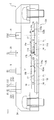
- the inner sides of the conductive terminal pins 18 to 20, 21a, 21b, 22a, and 22b are fixed to a supporting fixed die 30 and, in a state wherein sliding dies 31 and 32 are brought into contact with front and back end portions of the fixed die 30, as shown in Fig. 9 , an epoxy resin material of, for example, thermosetting resin is injected from, for example, the left end side of the fixed die 30, whereby the resin flows in the resin flow direction indicated by an arrow in Fig. 9 , and molding is carried out.
- an epoxy resin material of, for example, thermosetting resin is injected from, for example, the left end side of the fixed die 30, whereby the resin flows in the resin flow direction indicated by an arrow in Fig. 9 , and molding is carried out.
- the outline of the power semiconductor module 2 is formed overall as a cuboid molded body (sealing resin member) 24 forming a rectangular form in plan view, as shown in Fig. 1 .
- insulating wall portions 25A and 25B are formed in the molded body 24 at either end portion side in the longitudinal direction thereof, as shown in Fig. 1 .
- the insulating wall portions 25A and 25B are formed of a U-form protruding portion 25c, which is formed of a semi-cylindrical protruding portion 25a of a comparatively large diameter formed inwardly from the longitudinal direction end face of the molded body 24, and protruding from the surface thereof, and side wall portions 25b extending in a tangential direction from either end face of the semi-cylindrical protruding portion 25a to the end face of the molded body 24, and a depressed portion 26, which is contiguous with the inner peripheral surface of the U-form protruding portion 25c and hollowed out to a thickness approximately half that of the molded body 24, and the end face side thereof is opened.
- An attachment hole 27 centered on, for example, the central axis of the semi-cylindrical protruding portion 25a is formed penetrating to the bottom surface of the molded body 24 in a bottom portion of the depressed portion 26 configuring the insulating wall portions 25A and 25B.
- the inner diameter of the semi-cylindrical protruding portion 25a of the insulating wall portions 25A and 25B is set to be a diameter larger than the head portions of fixtures such as an attachment bolt and attachment screw inserted through the attachment hole 27, and the semi-cylindrical protruding portion 25a is set to have a wall face height such that the necessary creepage distance between the neighboring conductive terminal pins 18, 22a, and 22b and the head portions of the fixtures can be sufficiently secured.
- the conductive terminal pins 18 to 20 are individually connected to a main terminal bar, and the conductive terminal pins 21a, 21b, 22a, and 22b are connected via wire or printed wiring to a drive circuit, whereby it is possible to form, for example, a U-phase of an inverter circuit, and by three of this configuration being combined, it is possible to form a U-phase, a V-phase, and a W-phase.
- the transistors Q1a to Q1d and Q2a to Q2d of the main circuit components 13A and 13B installed in the power semiconductor module 2 are alternately controlled so as to be turned on and off so that when one group is in an on-state, the other group is in an off-state.
- the power semiconductor module 2 is such that, when taking the transistors Q1a to Q1d to be in an on-state and the transistors Q2a to Q2d to be in an off-state, a large current Ia input from the conductive terminal pin 18 forming the drain terminal D1 is supplied to the drain electrode 12Ad of the transistors Q1a to Q1d via the conductive pattern 14 of the main circuit component 13B, as indicated by the solid arrow in Fig. 3 .
- the current supplied to the conductive pattern 14 of the main circuit component 13A is output via the conductive terminal pin 19 to an inductive load as, for example, a U-phase output.
- the transistors Q2a to Q2d of the main circuit component 13A are maintained in an off-state, because of which no output current is obtained at the source terminal S2, and the conductive terminal pin 20 is maintained in a current cutoff state.
- the transistors Q2a to Q2d switch to an on-state, while the transistors Q1a to Q1d continue to be in an off-state.
- the current path between the main circuit component 13A, in which is mounted one group of the first semiconductor chip 12A and second semiconductor chip 12B, and the main circuit component 13B, in which is mounted the other group of the first semiconductor chip 12A and second semiconductor chip 12B, is formed from the first semiconductor chip 12A and second semiconductor chip 12B mounted on the conductor pattern 14 of the insulating substrate 11B, through the post electrode 17, via the main circuit wiring pattern 16b formed on the printed circuit board 16, and via the plurality of post electrodes 17b at an end portion on the main circuit wiring pattern 16a side, reaching the conductive pattern 14 (the chip mounting pattern 14c) of the insulating substrate 11A, as previously described.
- the signs of the current change rates (di/dt) of the currents flowing through the conductive pattern 14 of the main circuit component 13A and the main circuit wiring pattern 16a of the printed circuit board 16 being taken to be opposite signs, wherein one is positive and the other is negative, it is possible to reduce the mutual inductance M of the conductive pattern 14 of the main circuit component 13A and the main circuit wiring pattern 16a of the printed circuit board 16, and thus possible to ensure a high speed switching operation.
- the thickness of the conductive pattern 14 formed on the insulating substrates 11A and 11B of the main circuit components 13A and 13B being a copper pattern of 0. 5 mm or more, 1.5 mm or less
- the conductive terminal pins 18 to 20, 21a, 21b, 22a, and 22b forming external connection terminals are held by being press fitted.
- the thickness of the conductive pattern 14 being 0.5 mm or more, the conductive terminal pins 18 to 20, 21a, 21b, 22a, and 22b are reliably held in the fitting holes 14o, 14f, 14g, 14p, and 14q respectively, and mounting of the conductive terminal pin 18 and the like can be carried out easily.
- the diameter of the conductive terminal pins 18 to 20, 21a, 21b, 22a, and 22b being preferably in a range of 0.5 mm or more, 1.5 mm or less, is, for example, approximately 1.0 mm.
- the depth of the fitting holes 14o, 14f, 14g, 14p, and 14q is preferably within a range of 0.5 to 1.5 times the diameter of the conductive terminal pin 18 and the like, with the thickness of the conductive pattern 14 as the upper limit. Provided that the depth is within this range, the work of mounting the conductive terminal pin 18 and the like into the fitting hole 14o, and the like, formed in the conductive pattern 14 is easy.
- the thickness of the conductive pattern 14 is limited to 1.5 mm or less. The reason for this is that, when the thickness of the conductive pattern 14 exceeds 1.5 mm, becoming thick, etching for forming the conductive pattern 14 can no longer be carried out well due to side etching, and formation of an accurate pattern form becomes difficult.
- the thickness of the heat releasing heat transferring pattern 15 formed on the back surface side of the insulating substrates 11A and 11B is equal to the thickness of the conductive pattern 14.
- the thickness of the heat releasing heat transferring pattern 15 being less than 0.5 mm is undesirable from the aspect of cooling performance, and when the whole is sealed with a resin sealing member, as previously described, the thickness of the resin sealing member reaching the lower side of the substrate 13 decreases, and cracking is liable to occur in the resin sealing member, which is undesirable.
- the conductive pattern 14 formed on the insulating substrate 11A (or 11B) of the main circuit components 13A and 13B is such that the chip mounting pattern 14c (or 14j) on which the first semiconductor chip 12A and second semiconductor chip 12B are mounted is formed in a T-form of the wide portion 14a (or 14h) and narrow portion 14b (or 14i), and the terminal connection patterns 14d and 14e (or 14k, 141, 14m, and 14n) are formed independently on either outer side sandwiching the narrow portion 14b (or 14i). Therefore, the size of the substrate 13 can be reduced, and the size of the power semiconductor module 2 itself can also be reduced commensurately.
- the insulating substrates 11A and 11B are provided individually in the main circuit components 13A and 13B, and the conductive pattern 14 and heat releasing heat transferring pattern 15 are formed on each of the insulating substrates 11A and 11B, as in the embodiment, it is possible to suppress temperature rise due to heat generation occurring in the first semiconductor chip 12A and internal stress caused by a difference in linear expansion coefficients, and thus possible to further increase the reliability of the power semiconductor module 2.
- the pattern quantity of the conductive pattern 14 and heat releasing heat transferring pattern 15 formed on either surface of the substrate 13 of the main circuit components 13A and 13B can be such that the pattern quantity of the conductive pattern 14 is reduced, and the heat releasing heat transferring pattern 15 is disposed over practically the whole of the substrate 13. Therefore, the heat releasing area can be increased, and the heat releasing effect further increased.
- the narrow portions 14b and 14i of the T-form conductive pattern 14 not only act as current paths, but also contribute to heat transfer.
- the gate electrode of the first semiconductor chip 12A in the main circuit components 13A and 13B is formed on the side opposite to that of the second semiconductor chip 12B, the paths of the gate wiring patterns 16c and 16d can be disposed without crossing the main circuit wiring patterns 16a and 16b, and wiring layout can thus be carried out easily.
- the die for molding can be configured of the one fixed die 30 and the two sliding dies 31 and 32, as previously described using Fig. 9 . Consequently, die manufacture becomes easier, and there is no impediment to the flow of the resin sealing member, because of which good molding can be carried out at a good yield.
- the die for molding is such that it is necessary to provide three sliding dies 31, 32, and 33 that slide from three directions with respect to the one fixed die 30, as shown in Fig. 10 . Therefore, the die fabrication cost rises, the sliding die 33 impedes the flow of the resin sealing member, and the gate terminal and emitter auxiliary terminal are disposed so as form an obstacle in the resin flow direction, because of which portions that the resin sealing member does not reach appear, voids occur, and the like, which are factors in yield deterioration.
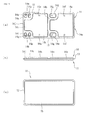
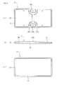
- the insulating substrates 11A and 11B are provided for each main circuit component 13A and 13B but, this not being limiting, the conductive pattern 14 for the main circuit components 13A and 13B, and a common heat releasing heat transferring pattern 15, may be formed on one substrate 13, as shown in Figs. 11 (a) to (c) , when the difference in the linear expansion coefficients of the members configuring the insulating substrate and the sealing member is not a problem, or the like.
- the insulating substrates 11A, 11B, and 11 not being limited to the heretofore described configuration, a so-called AMB (Active Metal Brazing) substrate, wherein a ceramic and copper are brazed and the copper is patterned by etching, or a DCB (Direct Copper Bonding) substrate wherein a ceramic substrate and copper are directly joined, can be applied.
- AMB Active Metal Brazing
- DCB Direct Copper Bonding
- alumina (Al 2 O 3 ), aluminum nitride (AlN), silicon nitride (Si 3 N 4 ), or the like can be applied as a ceramic substrate material.
- a resin substrate can be applied instead of a ceramic substrate. That is, it is sufficient that the substrate is such that insulation can be secured.
- all the terminals are installed in an insulating substrate but, this not being limiting, terminals through which a large current does not flow, such as the gate and source auxiliary terminals, may be installed directly in a printed board, as they do not need cooling.
- the insulating substrate 11 is such that two T-form chip mounting patterns 41 and 42 are disposed so that narrow portions 41a and 42a oppose each other, and terminal connection patterns 43a and 43b are formed independently on either outer side sandwiching the two narrow portions 41a.
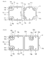
- narrow portions 51b and 51c may be formed on either side sandwiching a central wide portion 51a, as shown in Fig. 13 .
- wide portions 52b and 52c may be formed on either side sandwiching a central narrow portion 52a, as shown in Fig. 14 .
- RC-IGBT reverse conducting IGBT
- lead frames or other terminals can be applied instead of the conductive terminal pins 18 to 20, 21a, 21b, 22a, and 22b as external connection terminals. Also, the direction in which the terminals protrude not being limited to the upper surface of the power semiconductor module 2, the terminals may be caused to protrude from a side surface and bent upward.
- the invention is such that a desired circuit configuration is obtained simply by combining terminal connections of a semiconductor module
- the invention not being limited to the heretofore described power conversion inverter device, can be applied to another power conversion device using a power semiconductor module, or to another semiconductor device such as a high frequency application switching IC.
Landscapes
- Engineering & Computer Science (AREA)
- Microelectronics & Electronic Packaging (AREA)
- Manufacturing & Machinery (AREA)
- Physics & Mathematics (AREA)
- Thermal Sciences (AREA)
- Inverter Devices (AREA)
- Chemical & Material Sciences (AREA)
- Ceramic Engineering (AREA)
Abstract
Description
- The present invention relates to a semiconductor device in which is mounted a power semiconductor chip.
- A power semiconductor module is used in an inverter device configuring, for example, a power conversion device.
- The semiconductor device shown in, for example,
Fig. 15 has been proposed as an existing semiconductor device. - This existing semiconductor device is given as an example of, for example, a 2-in-1
semiconductor module 100. - The
semiconductor module 100 is such that a conductor patterned insulating substrate (ceramic insulating substrate) 102 is joined by asolder 103 onto a heat releasingmetal base plate 101. The conductor patternedinsulating substrate 102 has aceramic substrate 102a, and is configured of aconductor pattern 102b bonded to the front surface of theceramic substrate 102a and a back surfaceconductive film 102c bonded to the back surface of theceramic substrate 102a. - A semiconductor chip (semiconductor power chip) 104 is mounted across a
solder 105 on theconductor pattern 102b of the conductor patternedinsulating substrate 102. - Further, the
metal base plate 101, conductor patternedinsulating substrate 102, andsemiconductor chip 104 are disposed inside a box-form resin case 106 of which the lower end is opened, and fixed inside theresin case 106 by injecting a resin sealing material. 107 is a metal bar terminal that forms an external lead-out terminal soldered to theconductor pattern semiconductor chips 104, or thesemiconductor chip 104 and theconductor pattern 102b. - A highly reliable semiconductor device having excellent operating characteristics, and having high productivity, wherein deformation due to thermal expansion or the like is prevented by a semiconductor chip being disposed on a conductor patterned insulating substrate, a large number of post electrodes fixed to a printed circuit board being fixed to the semiconductor chip and conductor pattern, and a metal foil being formed on the front and back of the printed circuit board, thus securing heat releasing properties, has been proposed as another existing example (for example, refer to PTL 1).
- Also, there has also been proposed a power semiconductor module, which is a power semiconductor module formed of a series connection circuit of a power semiconductor device (IGBT) and a diode (FWD) connected in anti-parallel thereto, wherein the inductance value inside the power semiconductor module is reduced to practically zero by an electrode bar connected to a first power supply potential output electrode or the like, an electrode bar connected to an additional electrode or the like, and an electrode bar connected to a second power supply potential output electrode or the like each being formed in plate form, and disposed across an insulator in close proximity to each other (for example, refer to PTL 2).
- Furthermore, there has also been proposed a power semiconductor device wherein a rectangular ring-form wiring substrate is disposed on an upper portion of a bottom surface substrate so as to cover end and edge portions of the bottom surface substrate, a main collector electrode terminal and a main emitter electrode terminal are passed through an aperture portion in a central portion of the wiring substrate and caused to protrude from an aperture portion of a resin case, and a control emitter pad and gate pad are electrically connected via wires of equal length to a control emitter electrode and gate electrode (for example, refer to PTL 3).
- Further still, there has also been proposed a semiconductor device including a semiconductor device unit in which is sealed a semiconductor chip, a wiring substrate, and a bolt fastening unit, wherein at least the semiconductor device unit and bolt fastening unit are fixed using an elastic adhesive, and the semiconductor device unit is configured of a copper block, a conductor patterned insulating substrate, an IGBT chip, a diode chip, a collector terminal pin, a printed circuit board to which is fixed an implant pin, an emitter terminal pin, a control terminal pin, a collector terminal pin, and a resin case in which these are sealed (for example, refer to PTL 4).
- Also, there has been proposed a power semiconductor module including at least an insulating substrate, on which is mounted a power semiconductor chip and which has a copper plate and an insulating plate, a printed circuit board with pin connected to the power semiconductor chip, a connection terminal and insulating substrate connected to the copper plate, and a cuboid resin sealing member in the interior of which the printed circuit board with pin is encapsulated, wherein an emitter side connection terminal, a collector side connection terminal, and an output terminal are disposed in a row along a side edge of the resin sealing member on either side portion of the resin sealing member, and a gate terminal and emitter signal terminal are disposed in a row along one longitudinal direction end edge (for example, refer to PTL 5).
-
- PTL 1:
JP-A-2009-64852 - PTL 2:
JP-A-2004-214452 - PTL 3:
JP-A-2010-118699 - PTL 4:
JP-A-2011-142124 - PTL 5:
JP-A-2012-119618 - However, the heretofore described existing example illustrated in
Fig. 12 is such that, as there is a need to route thin bonding wire, it is difficult to reduce inductance in order to respond to high speed switching, and an external connection terminal is soldered to the conductor pattern, because of which there is an unresolved problem in that attachment of the external connection terminal cannot be carried out accurately. Furthermore, a pattern that routes wiring connected to the bonding wire has to be disposed on the insulating substrate, because of which size reduction is difficult, productivity and ease of assembly deteriorate, the structure becomes complex, and the heat releasing properties decrease. - Also, the existing example described in
PTL 1 is such that a post electrode (pin) shorter than bonding wire and with a larger sectional area is used, because of which inductance can be reduced, and two tier wiring of an insulating substrate and printed circuit board can be adopted, because of which size reduction is also possible. However, as no consideration is given to reducing the wiring inductance between the printed circuit board and insulating substrate, the existing configuration is insufficient for adequately fulfilling the capability of a high speed switching element typified by SiC or the like. Also, full mold technology using transfer molding or the like can be considered as means of forming a module inexpensively, but the form disclosed inPTL 1 is not necessarily suited to molding. - Furthermore, the existing example described in
PTL 2 is effective means in that wiring inductance can be reduced to practically zero by stacking current paths, and mutual inductance can be considerably reduced, but there are various demands regarding form in an actual semiconductor package, and in particular, when a pin form is adopted for an external terminal, and the external terminal is protruded upward, in order to be connected with the printed circuit board, or the like, it is clear that there exist regions in which positive electrode side and negative electrode side power supply wiring cannot be formed in a stacked structure, and even in places in which the wiring is stacked, mutual inductance can be reduced to "0" only in places in which the current directions are completely opposed, because of which it is difficult to rely only on this method. Furthermore, as it is often the case that a pad of a width of 1 mm or less is employed for a small semiconductor chip, it is difficult to mechanically join a plurality of chips while stacking bus bars. In the case of a small chip, employment of wire bonding and the post electrode described inPTL 1 is unavoidable. In particular, as is commonly known, it is often the case that SiC or the like is a small chip, because of the wafer defect density. - Also, generally, the smaller the module size, the thinner the wire becomes, and the more difficult it becomes to adopt a measure such as stacking, because of which it is often the case that inductance increases.
- Further still, the existing example described in PTL 3 is such that the main collector terminal and main emitter terminal are disposed on the bottom surface substrate via a main collector substrate and main emitter substrate, and the control emitter pad and gate pad are connected via wire to the IGBT element, connected to the wiring substrate via a control emitter relay terminal and gate relay terminal, and electrically connected to a control emitter electrode and gate electrode provided on the wiring substrate. Therefore, there is an unresolved problem in that the linking structure of an external connection terminal is complex, and ease of assembly and productivity decrease.
- Also, the existing example described in PTL 4 is such that, as the collector terminal pin is connected by soldering to a second copper block of the insulating substrate, and the emitter terminal pin and control terminal pin are connected to the printed circuit board, there is an unresolved problem in that disposition and connection of an external connection terminal cannot be carried out easily, and ease of assembly and productivity decrease.
- In the same way, the existing example described in PTL 5 is such that, as the collector side connection terminal and emitter side connection terminal are fixed to differing first copper plates of the insulating substrate, and the gate terminal and emitter signal terminal are fixed to the printed circuit board, there is an unresolved problem in that disposition and connection of an external connection terminal cannot be carried out easily, and ease of assembly and productivity decrease.
- Therefore, the invention, having been contrived focusing on the unresolved problems of the heretofore described existing examples, has an object of providing a semiconductor device such that, while being small, it is possible to achieve low inductance responding to high speed switching.
- In order to achieve the heretofore described object, a first aspect of a semiconductor device according to the invention includes a plurality of conductive pattern members, on each of which is mounted one or a plurality of power semiconductor chips, and a printed circuit board wherein a chip rod-form conductive connection member connected to the power semiconductor chip and a pattern rod-form conductive connection member connected to the conductive pattern member are disposed on the surface opposing the conductive pattern member. Further, the conductive pattern member is formed of a narrow portion and a wide portion, the narrow portion of at least one conductive pattern member and the printed circuit board are connected by the pattern rod-form conductive connection member, and a current path is formed between the conductive pattern member and the power semiconductor chip connected via the chip rod-form conductive connection member to the printed circuit board.
- Also, a second aspect of the semiconductor device according to the invention is such that a wiring pattern of the printed circuit board is disposed so that the signs of the change rate of current flowing through the conductive pattern member and the change rate of current flowing through the printed circuit board opposing the conductive pattern member are positive and negative opposite signs.
- Also, a third aspect of the semiconductor device according to the invention further includes a terminal connection pattern member formed on the outer side of the narrow portion and connecting an external connection terminal.
- Also, a fourth aspect of the semiconductor device according to the invention is such that the conductive pattern member is configured of a copper pattern of a thickness of 0.5 mm or more, 1.5 mm or less.
- Also, a fifth aspect of the semiconductor device according to the invention is such that the terminal connection pattern member is configured of a copper pattern of a thickness of 0.5 mm or more, which can hold the external connection terminal.
- Also, a sixth aspect of the semiconductor device according to the invention is such that the plurality of conductive pattern members are disposed on individual insulating substrates.
- Also, a seventh aspect of the semiconductor device according to the invention is such that the plurality of conductive pattern members are disposed on the same insulating substrate.
- Also, an eighth aspect of the semiconductor device according to the invention is such that a heat releasing heat transferring pattern member is formed on the side of the insulating substrate opposite to the surface on which the conductive pattern member is formed, and the number of heat releasing heat transferring pattern members is set to be the same as, or smaller than, the number of conductive pattern members.
- Also, a ninth aspect of the semiconductor device according to the invention is such that a main circuit wiring pattern is formed on both the front and back surface of the printed circuit board, and the two main circuit wiring patterns have the same potential.
- Also, a tenth aspect of the semiconductor device according to the invention further includes a sealing member encapsulating in the interior thereof the conductive pattern member and the printed circuit board, wherein the external connection terminals protrude in the same direction from the sealing member, and are disposed arrayed in the longitudinal direction of the sealing member.
- Also, an eleventh aspect of the semiconductor device according to the invention is such that the power semiconductor chip is configured of a voltage controlling semiconductor element having a gate electrode and a current detecting auxiliary electrode, and of wiring patterns formed on the printed circuit board, a wiring pattern connected to the gate electrode is formed on one surface of the printed circuit board, and a wiring pattern connected to the current detecting auxiliary electrode is formed in a position on the other surface of the printed circuit board opposing the wiring pattern connected to the gate electrode.
- The configuration may also be such that the main circuit component has a first semiconductor chip incorporating a semiconductor element and a second semiconductor chip incorporating a semiconductor rectifier element, the semiconductor element incorporated in the first semiconductor chip is configured of a voltage controlling semiconductor element having a gate electrode, and the gate electrode is disposed so as to be positioned on an end surface side on the side opposite to that of the end surface opposing the second semiconductor chip.
- Also, a twelfth aspect of the semiconductor device according to the invention is such that the power semiconductor chip is configured of a voltage controlling semiconductor element having a main electrode, a wiring pattern member connected to the main electrode is formed on both the front and back surface of the printed circuit board, and the two wiring pattern members have the same potential.
- Also, a thirteenth aspect of the semiconductor device according to the invention is such that the power semiconductor chip is configured of a voltage controlling semiconductor element having a gate electrode, and the power semiconductor chip is disposed so that the gate electrode is positioned on the outer side of the insulating substrate in a longitudinal direction when a plurality of the insulating substrates are disposed.
- Also, a fourteenth aspect of a semiconductor device according to the invention includes a plurality of conductive pattern members, on each of which is mounted one or a plurality of power semiconductor chips; and a printed circuit board wherein a chip rod-form conductive connection member connected to the power semiconductor chip and a pattern rod-form conductive connection member connected to the conductive pattern member are disposed on the surface opposing the conductive pattern member. Further, a wiring pattern of the printed circuit board is disposed so that the signs of the change rate of current flowing through the conductive pattern member and the change rate of current flowing through the printed circuit board opposing the conductive pattern member are positive and negative opposite signs.
- According to the invention, a conductor pattern formed on an insulating substrate is formed of a narrow portion, and of a wide portion on which a semiconductor chip is mounted, and a current path is formed between a plurality of main circuit component parts by the narrow portion of the conductive pattern and a printed circuit board being connected by a rod-form conductive connection member. Therefore, it is possible to provide a small semiconductor device such that it is possible to adopt a configuration wherein inductance is reduced without increasing the dimensions, and resin molding is easy, and it is thus possible to respond to a high speed switching element.
-
- [
Fig. 1] Fig. 1 is perspective views showing an embodiment of a semiconductor device according to the invention, wherein (a) is a perspective view seen from a planar surface side, while (b) is a perspective view seen from a bottom surface side. - [
Fig. 2] Fig. 2 is a plan view of an insulating substrate on which a semiconductor chip is mounted. - [
Fig. 3] Fig. 3 is a sectional view of the semiconductor device ofFig. 1 along a line A-A ofFig. 2 . - [
Fig. 4] Fig. 4 is diagrams showing an insulating substrate applicable to the invention, wherein (a) is a plan view, (b) is a side view, and (c) is a bottom view. - [
Fig. 5] Fig. 5 is diagrams showing a printed circuit board applicable to the invention, wherein (a) is a plan view and (b) is a bottom view. - [
Fig. 6] Fig. 6 is a circuit diagram showing an equivalent circuit of the semiconductor device. - [
Fig. 7] Fig. 7 is a circuit diagram showing a current path when a transistor Q1a ofFig. 6 is inverted from an on-state to an off-state. - [
Fig. 8] Fig. 8 is a perspective view showing a state wherein the printed circuit board is mounted on the insulating substrate. - [
Fig. 9] Fig. 9 is a plan view showing a resin sealing die applicable to the invention. - [
Fig. 10] Fig. 10 is a plan view showing an existing resin sealing die. - [
Fig. 11] Fig. 11 is diagrams showing a first modification example of an insulating substrate, wherein (a) is a plan view, (b) is a side view, and (c) is a bottom view. - [
Fig. 12] Fig. 12 is diagrams showing a second modification example of an insulating substrate, wherein (a) is a plan view, (b) is a side view, and (c) is a bottom view. - [
Fig. 13] Fig. 13 is a plan view showing a third modification example of an insulating substrate. - [
Fig. 14] Fig. 14 is a plan view showing a fourth modification example of an insulating substrate. - [
Fig. 15] Fig. 15 is a sectional view showing an existing example. - Hereafter, referring to the drawings, a description will be given of an embodiment of the invention.
-
Fig. 1 is perspective views showing a semiconductor device according to the invention. - In the drawing, 2 is a power semiconductor module acting as a semiconductor device. The
power semiconductor module 2 includes, as is particularly clear inFig. 2 to Fig. 8 , a pair ofmain circuit components first semiconductor chip 12A and asecond semiconductor chip 12B, mounted on insulatingsubstrates circuit board 16 configuring a common wiring circuit above themain circuit components - The
first semiconductor chip 12A is configured incorporating a power MOSFET (Metal-Oxide-Semiconductor Field-Effect Transistor) (or an insulated gate bipolar transistor (IGBT)). Thesecond semiconductor chip 12B is configured incorporating a free wheeling diode (FWD). - Further, as shown in
Fig. 2 , two of thesecond semiconductor chip 12B are disposed maintaining a predetermined interval on a longitudinal direction (a left-right direction in the drawing) central line on the insulatingsubstrate 11A, and two each of thefirst semiconductor chip 12A are disposed maintaining a predetermined distance on either outer side of the second semiconductor chips 12B. Two of thesecond semiconductor chip 12B, and four of thefirst semiconductor chip 12A sandwiching thesecond semiconductor chips 12B, are disposed in the same way on the insulatingsubstrate 11B too. - Herein, the
first semiconductor chip 12A has a drain electrode 12Ad, a source electrode 12As, and a gate electrode 12Ag, wherein the gate electrode 12Ag is disposed so as be on an end portion side (insulating substrate outer side) on the side opposite to that of thesecond semiconductor chip 12B. - Although the
semiconductor chips - The insulating
substrate 11A has asubstrate 13 of, for example, a square form with a ceramic such as alumina, with good heat conductivity, as a main component, aconductive pattern 14 acting as a conductive pattern member configured of a copper plate with a thickness of 0.5 mm or more is bonded to the front surface of thesubstrate 13, and a heat releasingheat transferring pattern 15 having the same thickness is bonded to the back surface of thesubstrate 13. - The
conductive pattern 14, as shown inFig. 2 andFig. 3 , has achip mounting pattern 14c, the planar form of which is a protruding (T) form. Thechip mounting pattern 14c includes awide portion 14a, of which an end portion on the right side in the drawing has a width practically equal to the width of thesubstrate 13, and anarrow portion 14b, contiguous with the left side of thewide portion 14a, of a width smaller than that of thewide portion 14a. - Also, the
conductive pattern 14 has independentterminal connection patterns narrow portion 14b of thechip mounting pattern 14c. Side edges of theterminal connection patterns wide portion 14a of thechip mounting pattern 14c. - Herein, as shown in
Fig. 2 , thefirst semiconductor chip 12A andsecond semiconductor chip 12B are mounted across a joining member such as solder on thewide portion 14a of thechip mounting pattern 14c, and twofitting holes 14f are formed on the width direction outer sides of thefirst semiconductor chip 12A. A conductiveterminal pin 19 forming a main circuit external connection terminal is press fitted into thefitting hole 14f. Also, afitting hole 14g is formed in each of theterminal connection patterns terminal pin 20 forming a source terminal S2 that acts as an external connection terminal is press fitted into thefitting hole 14g. - Also, in the same way as the insulating
substrate 11A, the insulatingsubstrate 11B also has thesubstrate 13 with a ceramic as a main component, and theconductive pattern 14 and heat releasingheat transferring pattern 15 formed on the front and back of thesubstrate 13. Theconductive pattern 14 has achip mounting pattern 14j, the planar form of which is a protruding (T) form. Thechip mounting pattern 14j, in the same way as on the insulatingsubstrate 11A, includes awide portion 14h and anarrow portion 14i. Pairs ofterminal connection patterns narrow portion 14i of thechip mounting pattern 14j. - Further, as shown in
Fig. 2 , thefirst semiconductor chip 12A andsecond semiconductor chip 12B are mounted across a joining member such as solder on thechip mounting pattern 14j, and twofitting holes 140 are formed on the width direction outer sides of thefirst semiconductor chip 12A. A conductiveterminal pin 18 forming a drain terminal that acts as an external connection terminal is press fitted into the fitting hole 14o. Afitting hole 14p is formed in each of theterminal connection patterns fitting holes 14p. Afitting hole 14q is formed in each of theterminal connection patterns fitting holes 14q. - Herein, it is desirable that the material of the conductive terminal pins 18, 20, and 19 is copper (Cu) or of an aluminum (Al) series, which have excellent conductivity. However, when considering ease of solder joining, mounting efficiency can be increased by carrying out surface treatment on the conductive terminal pins 18, 20, and 19 using nickel (Ni) or a tin series, thereby improving the leakage of the solder joint.
- As is clear from the equivalent circuit diagram shown in
Fig. 6 , an anti-parallel connection circuit including, for example, N-channel MOSFETs (hereafter referred to simply as transistors) Q1a to Q1d forming thefirst semiconductor chips 12A and FWDs (hereafter referred to as diodes) Di1a and Di1b forming thesecond semiconductor chips 12B, which configure an upper arm, are formed on theconductive pattern 14 of the insulatingsubstrate 11B. An anti-parallel circuit including transistors Q2a to Q2d forming thefirst semiconductor chips 12A and diodes Di2a and Di2b forming the second semiconductor chips, which configure a lower arm, are formed on theconductive pattern 14 of the insulatingsubstrate 11A. The two anti-parallel circuits are connected in series. - Herein, as it is sufficient that the semiconductor chips (power devices) disposed on one of the insulating
substrates Fig. 6 are configured equivalently, there may be one each of the transistors and diodes, or there may be the same multiple of both. - Further, the two anti-parallel circuits formed of one pair of the transistors Q1a to Q1d and Q2a to Q2d and the diodes Di1a, Di1b, Di2a, and Di2b are connected in series to the printed
circuit board 16 disposed in an upper plane via acylindrical post electrode 17 acting as a rod-form conductive connection member. - As shown in
Fig. 2 , the twosemiconductor chips - Further, a drain electrode 12Ad of the transistors Q1a to Q1d (or Q2a to Q2d) is formed on the lower surface of the
first semiconductor chip 12A, and is connected via thechip mounting pattern 14j (or 14c) of theconductive pattern 14 to the conductiveterminal pin 18 acting as a connection terminal configuring an external input terminal (drain terminal D1) (or to the conductiveterminal pin 19 forming a main circuit external connection terminal (source/drain terminal S1/D2)) of thepower semiconductor module 2. A cathode electrode formed on the back surface of thesecond semiconductor chip 12B is also connected via thechip mounting pattern 14j (or 14c) to the conductive terminal pin 18 (or conductive terminal pin 19). - Also, the source electrode 12As and gate electrode 12Ag of the transistors Q1a to Q1d (or Q2a to Q2d) are formed on the front surface of the
first semiconductor chip 12A, and each is connected to the printedcircuit board 16 via thepost electrode 17 acting as a chip rod-form conductive connection member. - Herein, although the source electrode 12As and gate electrode 12Ag of the transistors Q1a to Q1d (or Q2a to Q2d) are connected to the wiring pattern formed on the printed
circuit board 16, the wiring pattern connected to a gate electrode is formed on one surface of the printedcircuit board 16, while the wiring pattern connected to a source sense electrode (not shown) is formed in a position on the other surface of the printedcircuit board 16 opposing the wiring pattern connected to the gate electrode. - By disposing the conductor pattern connected to the gate electrode and the wiring pattern connected to the source sense electrode in this way, it is possible to reduce the mutual inductance between the two wiring patterns. By reducing the mutual inductance, it is possible to stabilize control of the transistors Q1a to Q1d (or Q2a to Q2d). In particular, reducing the mutual inductance is effective in restricting false firing caused by the effect of wiring inductance.
- Also, an anode electrode is formed on the front surface of the
second semiconductor chip 12B, and the anode electrode is connected to the printedcircuit board 16 via thepost electrode 17 acting as a chip rod-form conductive connection member. - As shown in
Fig. 1 , the conductive terminal pins 18 to 20 are formed one each in positions symmetrical across a width direction central line of thepower semiconductor module 2. Also, thepower semiconductor module 2 further has a total of fourconductive terminal pins terminal pin 18. The conductive terminal pins 18 to 20 and 21a, 21b, 22a, and 22b are disposed in two rows in a practically straight line along the two side edges of thepower semiconductor module 2. - The conductive terminal pins 21a and 21b are source auxiliary terminals and configure current detecting terminals SS1 and SS2, which are connected to the printed
circuit board 16, connected to sources that sense current flowing between the drain and source of the transistors Q1a to Q1d and Q2a to Q2d, and output sense signals. Also, the remaining two conductive terminal pins 22a and 22b configure gate terminals G1 and G2, which are connected to the printedcircuit board 16 and supply gate control signals to the gate electrodes of the half-bridge circuit transistors Q1a to Q1d and Q2a to Q2d. - Also, the heat releasing
heat transferring pattern 15 on the back surface side of the insulatingsubstrates conductive pattern 14, and the lower surface of the heat releasingheat transferring pattern 15 is flush with the bottom surface of thepower semiconductor module 2, or protrudes slightly from the bottom surface. - As shown in
Figs. 5 (a) and (b) , the printedcircuit board 16 is such that a wide maincircuit wiring pattern 16a of a T-form whose stem faces right, which forms a circuit path of themain circuit component 13A, and a similarly wide maincircuit wiring pattern 16b, which forms a circuit path of themain circuit component 13B, are formed on the front surface side. Also,gate wiring patterns post electrode 17 to the gate electrodes of thefirst semiconductor chips 12A of themain circuit components circuit board 16. - The
gate wiring pattern 16c is configured of a crown-form pattern 16e and aconnection pattern 16h. The crown-form pattern 16e is formed so as to enclose the narrow portion of the T-form wiring pattern 16a, maintaining a predetermined distance. Theconnection pattern 16h is extended along a side edge of the printedcircuit board 16 so as to link a central portion of the crown-form pattern 16e and aterminal connection pattern 16g. Theterminal connection pattern 16g is formed on the periphery of aninsertion hole 16f, pierced in a left end portion of the printedcircuit board 16, for inserting the conductiveterminal pin 22a. - The
gate wiring pattern 16d is configured of a crown-form pattern 16j and aconnection pattern 16m. The crown-form pattern 16j is formed so as to enclose a left side end portion of theconductor pattern 16b. Theconnection pattern 16m is formed in an approximate L-form so as to link a central portion of the crown-form pattern 16j and aterminal connection pattern 161. Theterminal connection pattern 161 is formed on the periphery of aninsertion hole 16k, pierced in a left end portion of the printedcircuit board 16, for inserting the conductiveterminal pin 22b. - Simple insertion holes 16o and 16p, through which the conductive terminal pins 18 and 19 are inserted contactlessly, and a through
hole 16q, through which the conductiveterminal pin 20 is inserted contactlessly, are pierced in the printedcircuit board 16. - Herein, it is taken that the through
hole 16q is not in contact with the conductiveterminal pin 20, but when further inductance reduction is necessary, the wiring length can be reduced by the throughhole 16q and conductiveterminal pin 20 being electrically connected by soldering or the like. - Furthermore, as shown in
Fig. 5 (b) , the wide maincircuit wiring pattern 16a of a T-form whose stem faces right, which forms a circuit path of themain circuit component circuit board 16 so as to coincide with the front surface side maincircuit wiring patterns terminal wiring patterns post electrode 17 to an anode of the diode Di1a of themain circuit component 13A and an anode of the diode Di2a of themain circuit component 13B, are formed on the back surface of the printedcircuit board 16. The source senseterminal wiring patterns gate wiring patterns terminal connection patterns insertion holes circuit board 16. - Herein, an end portion on the main
circuit wiring pattern 16a side of the maincircuit wiring pattern 16b on the front and back of the printedcircuit board 16 is electrically connected to thenarrow portion 14b of thechip mounting pattern 14c of the insulatingsubstrate 11A by a plurality, for example six, of apost electrode 17b acting as pattern rod-form conductive connection members, whereby a current path is formed by thepost electrodes 17b between themain circuit components circuit wiring pattern 16b in which thepost electrodes 17b are provided is disposed in a cutaway portion on the left side of the maincircuit wiring pattern 16a, whereby it is possible to reduce the size of the semiconductor device while maintaining the area over which the maincircuit wiring pattern 16a andchip mounting pattern 14c coincide, which is desirable. - Also, the main
circuit wiring patterns 16a on the front and back of the printedcircuit board 16 are set to have the same potential as each other, and in the same way, the front andback conductor patterns 16b are also set to have the same potential as each other. - Further, in a state wherein the conductive terminal pins 18 to 20, 21a, 21b, 22a, and 22b are press fitted into the
main circuit components main circuit components circuit board 16 are joined, as shown inFig. 8 . In this case, the conductive terminal pins 19, 18, 20, 21a, 21b, 22a, and 22b are inserted respectively through theinsertion holes circuit board 16. - Also, the
post electrodes 17 forming chip rod-form conductive connection members formed in the printedcircuit board 16 are brought into contact across solder with thefirst semiconductor chip 12A andsecond semiconductor chip 12B, while thepost electrodes 17b forming pattern conductive connection members are brought into contact across solder with theconductor pattern 14a of the insulatingsubstrate 11A. By a reflow process being carried out in this state, thepost electrodes 17 and postelectrodes 17b of the printedcircuit board 16 are electrically and mechanically joined to thefirst semiconductor chip 12A andsecond semiconductor chip 12B, and to theconductive pattern 14. - Simultaneously with this, the main
circuit wiring pattern 16a of the printedcircuit board 16 is electrically joined to theterminal connection patterns substrate 11A viapost electrodes 17a acting as pattern rod-form conductive connection members. Also, theterminal connection patterns circuit board 16 are electrically connected to theterminal connection patterns substrate 11A via, in the same way,post electrodes 17a. Furthermore, theterminal connection patterns circuit board 16 are electrically joined to theterminal connection patterns substrate 11A via, in the same way,post electrodes 17a. - After the
main circuit components circuit board 16 are joined in this way, the inner sides of the conductive terminal pins 18 to 20, 21a, 21b, 22a, and 22b are fixed to a supporting fixeddie 30 and, in a state wherein sliding dies 31 and 32 are brought into contact with front and back end portions of the fixeddie 30, as shown inFig. 9 , an epoxy resin material of, for example, thermosetting resin is injected from, for example, the left end side of the fixeddie 30, whereby the resin flows in the resin flow direction indicated by an arrow inFig. 9 , and molding is carried out. At this time, as the conductive terminal pins 18 to 20, 21a, 21b, 22a, and 22b are disposed in the resin flow direction, there is no impediment to the resin flow, and it is possible to prevent the occurrence of a smooth void, thus improving adhesion. - By molding being carried out in this way, the outline of the
power semiconductor module 2 is formed overall as a cuboid molded body (sealing resin member) 24 forming a rectangular form in plan view, as shown inFig. 1 . - Further, insulating
wall portions body 24 at either end portion side in the longitudinal direction thereof, as shown inFig. 1 . The insulatingwall portions portion 25c, which is formed of a semi-cylindricalprotruding portion 25a of a comparatively large diameter formed inwardly from the longitudinal direction end face of the moldedbody 24, and protruding from the surface thereof, andside wall portions 25b extending in a tangential direction from either end face of the semi-cylindrical protrudingportion 25a to the end face of the moldedbody 24, and adepressed portion 26, which is contiguous with the inner peripheral surface of theU-form protruding portion 25c and hollowed out to a thickness approximately half that of the moldedbody 24, and the end face side thereof is opened. - An
attachment hole 27 centered on, for example, the central axis of the semi-cylindrical protrudingportion 25a is formed penetrating to the bottom surface of the moldedbody 24 in a bottom portion of thedepressed portion 26 configuring the insulatingwall portions portion 25a of the insulatingwall portions attachment hole 27, and the semi-cylindrical protrudingportion 25a is set to have a wall face height such that the necessary creepage distance between the neighboring conductive terminal pins 18, 22a, and 22b and the head portions of the fixtures can be sufficiently secured. - Further, in a state wherein a required number of the
power semiconductor module 2 having the heretofore described configuration are disposed in parallel, the conductive terminal pins 18 to 20 are individually connected to a main terminal bar, and the conductiveterminal pins - When configuring, for example, an inverter device in this way, the transistors Q1a to Q1d and Q2a to Q2d of the
main circuit components power semiconductor module 2 are alternately controlled so as to be turned on and off so that when one group is in an on-state, the other group is in an off-state. - Therefore, the
power semiconductor module 2 is such that, when taking the transistors Q1a to Q1d to be in an on-state and the transistors Q2a to Q2d to be in an off-state, a large current Ia input from the conductiveterminal pin 18 forming the drain terminal D1 is supplied to the drain electrode 12Ad of the transistors Q1a to Q1d via theconductive pattern 14 of themain circuit component 13B, as indicated by the solid arrow inFig. 3 . - Current output from the source electrode 12As of the transistors Q1a to Q1d passes through the main
circuit wiring pattern 16b of the printedcircuit board 16 via thepost electrode 17, and is supplied via thepost electrode 17b to theconductive pattern 14 of themain circuit component 13A. - The current supplied to the
conductive pattern 14 of themain circuit component 13A is output via the conductiveterminal pin 19 to an inductive load as, for example, a U-phase output. - At this time, the transistors Q2a to Q2d of the
main circuit component 13A are maintained in an off-state, because of which no output current is obtained at the source terminal S2, and the conductiveterminal pin 20 is maintained in a current cutoff state. - When expressing the heretofore described current path as an equivalent circuit with the transistors Q1a to Q1d represented by the transistor Q1a, current input from the drain terminal D1 (the conductive terminal pin 18) is output from the drain of the transistor Q1a through the source to the S1D2 terminal (the conductive terminal pin 19) forming an output terminal, as indicated by a solid line in
Fig. 7 . - When the transistors Q1a to Q1d of the
main circuit component 13B switch from this state to an off-state, the current Ia shown by solid lines inFig. 3 andFig. 7 decreases, but owing to the effect of the inductive load, the output current of the S1D2 terminal (the conductive terminal pin 19) forming an output terminal continues. The shortfall is compensated for by a supply from the source terminal S2 (the conductive terminal pin 20) via the free wheeling diodes Di2a and Di2b of themain circuit component 13A, as indicated by the dotted line inFig. 7 . - When expressing this current path in
Fig. 3 , current input from the conductive terminal pin 20 (the source terminal S2) is supplied from theterminal connection patterns conductive pattern 14 of the insulatingsubstrate 11A via thepost electrode 17a to the maincircuit wiring pattern 16a of the printedcircuit board 16, as indicated by the dotted line. - Current supplied to the main
circuit wiring pattern 16a is supplied via thepost electrode 17 from an anode 12Ba of the free wheeling diode Di2a (thesemiconductor chip 12B), through a cathode 12Bk, to theconductor pattern 14a in theconductive pattern 14 of the insulatingsubstrate 11A. - Current supplied to the
conductor pattern 14a is supplied through the conductive terminal pin 19 (the output terminal S1D2) to the inductive load. - At this time, current passing through the transistor Q1a decreases while current passing through the free wheeling diode Di2a increases, the currents pass through the mutually opposing
conductor patterns substrate 11A and through the maincircuit wiring pattern 16a of the printedcircuit board 16, eventually come together in the conductiveterminal pin 19, and are output to the inductive load. - Therefore, the current indicated by the solid line decreases in the
conductor pattern 14a of themain circuit component 13A, and the current change rate di/dt becomes, for example, negative, while the current passing through the maincircuit wiring pattern 16a of the printedcircuit board 16 indicated by the dotted line increases, and the current change rate di/dt becomes, for example, positive. Therefore, self inductance L1 of theconductive pattern 14 and self inductance L2 of the maincircuit wiring pattern 16a of the printedcircuit board 16 are connected in series and, taking the mutual inductance of the two to be M, an inter-terminal voltage v can be expressed by the following equation.
- Consequently, as the current change rate di/dt of the
conductor pattern 14a of themain circuit component 13A is negative, and the current change rate di/dt of the maincircuit wiring pattern 16a of the printedcircuit board 16 is positive, the mutual inductance M can be cancelled out. - Subsequently, after a predetermined dead time elapses, the transistors Q2a to Q2d switch to an on-state, while the transistors Q1a to Q1d continue to be in an off-state.
- In this way, according to the embodiment, the current path between the
main circuit component 13A, in which is mounted one group of thefirst semiconductor chip 12A andsecond semiconductor chip 12B, and themain circuit component 13B, in which is mounted the other group of thefirst semiconductor chip 12A andsecond semiconductor chip 12B, is formed from thefirst semiconductor chip 12A andsecond semiconductor chip 12B mounted on theconductor pattern 14 of the insulatingsubstrate 11B, through thepost electrode 17, via the maincircuit wiring pattern 16b formed on the printedcircuit board 16, and via the plurality ofpost electrodes 17b at an end portion on the maincircuit wiring pattern 16a side, reaching the conductive pattern 14 (thechip mounting pattern 14c) of the insulatingsubstrate 11A, as previously described. Therefore, it is possible to carry out an electrical connection of theconductive pattern 14 of the insulatingsubstrate 11A and the printedcircuit board 16 using thepost electrodes 17b, possible to shorten the wiring distance and increase the sectional area of the current path, and thus possible to reduce the wiring inductance. - Moreover, by the signs of the current change rates (di/dt) of the currents flowing through the
conductive pattern 14 of themain circuit component 13A and the maincircuit wiring pattern 16a of the printedcircuit board 16 being taken to be opposite signs, wherein one is positive and the other is negative, it is possible to reduce the mutual inductance M of theconductive pattern 14 of themain circuit component 13A and the maincircuit wiring pattern 16a of the printedcircuit board 16, and thus possible to ensure a high speed switching operation. - Furthermore, with the thickness of the
conductive pattern 14 formed on the insulatingsubstrates main circuit components conductive pattern 14 being 0.5 mm or more, the conductive terminal pins 18 to 20, 21a, 21b, 22a, and 22b are reliably held in thefitting holes terminal pin 18 and the like can be carried out easily. At this time, by forming a plating layer to be melted by a reflow process on the inner peripheral surfaces of the fitting holes of theconductive pattern 14 in which the conductive terminal pins 18 to 20, 21a, 21b, 22a, and 22b are press fitted, holding of the conductiveterminal pin 18 and the like can be carried out still more easily, and reliability increases commensurately. - The diameter of the conductive terminal pins 18 to 20, 21a, 21b, 22a, and 22b, being preferably in a range of 0.5 mm or more, 1.5 mm or less, is, for example, approximately 1.0 mm. When the diameter is less than 0.5 mm, inductance increases, and when the diameter is greater than 1.5 mm, soldering of the pins and other members is difficult. Also, the depth of the
fitting holes terminal pin 18 and the like, with the thickness of theconductive pattern 14 as the upper limit. Provided that the depth is within this range, the work of mounting the conductiveterminal pin 18 and the like into the fitting hole 14o, and the like, formed in theconductive pattern 14 is easy. - Also, the thickness of the
conductive pattern 14 is limited to 1.5 mm or less. The reason for this is that, when the thickness of theconductive pattern 14 exceeds 1.5 mm, becoming thick, etching for forming theconductive pattern 14 can no longer be carried out well due to side etching, and formation of an accurate pattern form becomes difficult. - Also, in order to prevent bending of the insulating
substrates heat transferring pattern 15 formed on the back surface side of the insulatingsubstrates conductive pattern 14. The thickness of the heat releasingheat transferring pattern 15 being less than 0.5 mm is undesirable from the aspect of cooling performance, and when the whole is sealed with a resin sealing member, as previously described, the thickness of the resin sealing member reaching the lower side of thesubstrate 13 decreases, and cracking is liable to occur in the resin sealing member, which is undesirable. - Moreover, the
conductive pattern 14 formed on the insulatingsubstrate 11A (or 11B) of themain circuit components chip mounting pattern 14c (or 14j) on which thefirst semiconductor chip 12A andsecond semiconductor chip 12B are mounted is formed in a T-form of thewide portion 14a (or 14h) andnarrow portion 14b (or 14i), and theterminal connection patterns narrow portion 14b (or 14i). Therefore, the size of thesubstrate 13 can be reduced, and the size of thepower semiconductor module 2 itself can also be reduced commensurately. - Furthermore, as the insulating
substrates main circuit components conductive pattern 14 and heat releasingheat transferring pattern 15 are formed on each of the insulatingsubstrates first semiconductor chip 12A and internal stress caused by a difference in linear expansion coefficients, and thus possible to further increase the reliability of thepower semiconductor module 2. - Further still, the pattern quantity of the
conductive pattern 14 and heat releasingheat transferring pattern 15 formed on either surface of thesubstrate 13 of themain circuit components conductive pattern 14 is reduced, and the heat releasingheat transferring pattern 15 is disposed over practically the whole of thesubstrate 13. Therefore, the heat releasing area can be increased, and the heat releasing effect further increased. In this case, thenarrow portions conductive pattern 14 not only act as current paths, but also contribute to heat transfer. This is because, as a copper pattern generally has far better heat conductivity than an insulator such as a ceramic, heat is not only transferred immediately below the semiconductor chip, but also spreads to thenarrow portions heat transferring pattern 15 on the cooling surface side, and further spreads over the whole of the cooling surface. - Also, as the gate electrode of the
first semiconductor chip 12A in themain circuit components second semiconductor chip 12B, the paths of thegate wiring patterns circuit wiring patterns - Furthermore, as the conductive terminal pins 18 to 20, 21a, 21b, 22a, and 22b are disposed in two rows in a practically straight line along the longitudinal direction side edges of the
power semiconductor module 2, the die for molding can be configured of the one fixeddie 30 and the two sliding dies 31 and 32, as previously described usingFig. 9 . Consequently, die manufacture becomes easier, and there is no impediment to the flow of the resin sealing member, because of which good molding can be carried out at a good yield. - Herein, when providing a gate terminal and an emitter auxiliary terminal on a longitudinal direction end surface side of a power semiconductor module, as described in PTL 5, the die for molding is such that it is necessary to provide three sliding dies 31, 32, and 33 that slide from three directions with respect to the one fixed
die 30, as shown inFig. 10 . Therefore, the die fabrication cost rises, the slidingdie 33 impedes the flow of the resin sealing member, and the gate terminal and emitter auxiliary terminal are disposed so as form an obstacle in the resin flow direction, because of which portions that the resin sealing member does not reach appear, voids occur, and the like, which are factors in yield deterioration. - In the embodiment, a description has been given of a case wherein the insulating
substrates main circuit component conductive pattern 14 for themain circuit components heat transferring pattern 15, may be formed on onesubstrate 13, as shown inFigs. 11 (a) to (c) , when the difference in the linear expansion coefficients of the members configuring the insulating substrate and the sealing member is not a problem, or the like. - Also, in the embodiment, the insulating
substrates - Also, in the embodiment, a description has been given of a case wherein the printed
circuit board 16 and theconductive pattern 14 andsemiconductor chips substrates cylindrical post electrodes - Also, in the embodiment, all the terminals are installed in an insulating substrate but, this not being limiting, terminals through which a large current does not flow, such as the gate and source auxiliary terminals, may be installed directly in a printed board, as they do not need cooling. In this case, it is sufficient that the insulating
substrate 11 is such that two T-formchip mounting patterns narrow portions 41a and 42a oppose each other, andterminal connection patterns narrow portions 41a. In this case, compared with the heretofore described embodiment, problems occur in that there is a decrease in ease of assembly caused by standing terminals in two places, in the insulating substrate and printed circuit board, that the terminals standing in the printed circuit board are unstable when molding resin, and the like, but there are advantages in that the chip mounting pattern area increases, and cooling performance improves. - Also, in the embodiment, a description has been given of a case wherein one each of a narrow portion and wide portion are formed as a chip mounting pattern but, this not being limiting,
narrow portions wide portion 51a, as shown inFig. 13 . Furthermore,wide portions narrow portion 52a, as shown inFig. 14 . - Also, in the embodiment, a description has been given of a case wherein a power MOSFET is incorporated in the
first semiconductor chip 12A but, this not being limiting, an IGBT may be incorporated in thefirst semiconductor chip 12A, or another voltage controlling semiconductor element may be incorporated. Also, instead of the combination of thefirst semiconductor chip 12A andsecond semiconductor chip 12B, a reverse conducting IGBT (RC-IGBT) incorporating a FWD may be used as thefirst semiconductor chip 12A. - Also, in the embodiment, a description has been given of a case wherein a plurality of the
first semiconductor chip 12A andsecond semiconductor chip 12B are disposed on the insulatingsubstrates second semiconductor chip 12B and configure using only thefirst semiconductor chip 12A when it is possible to use a diode incorporating a transistor, when a motive rectification method is employed, and the like. - Also, lead frames or other terminals can be applied instead of the conductive terminal pins 18 to 20, 21a, 21b, 22a, and 22b as external connection terminals. Also, the direction in which the terminals protrude not being limited to the upper surface of the
power semiconductor module 2, the terminals may be caused to protrude from a side surface and bent upward. - Also, as the invention is such that a desired circuit configuration is obtained simply by combining terminal connections of a semiconductor module, the invention, not being limited to the heretofore described power conversion inverter device, can be applied to another power conversion device using a power semiconductor module, or to another semiconductor device such as a high frequency application switching IC.
- 1 ... Semiconductor device, 2 ... Power semiconductor module, 11A, 11B ... Insulating substrate, 12A ... First semiconductor chip, 12B ... Second semiconductor chip, 13A, 13B ... Main circuit component path, 14 ... Conductive pattern, 14a, 14h ... Wide portion, 14b, 14i ... Narrow portion, 14c, 14j ... Chip mounting pattern, 14c, 14e, 14k, 141, 14m, 14n ... Terminal connection pattern, 15 ... Heat releasing heat transferring pattern, 16 ... Printed circuit board, 18 to 20, 21a, 21b, 22a, 22b ... Conductive terminal pin, 24 ... Molded body, 30 ... Fixed die, 31, 32 ... Sliding die
Claims (15)
- A semiconductor device, comprising:a plurality of conductive pattern members, on each of which is mounted one or a plurality of power semiconductor chips; anda printed circuit board on which are disposed a chip rod-form conductive connection member connected to the power semiconductor chip and a pattern rod-form conductive connection member connected to the conductive pattern member, whereinthe conductive pattern member is formed of a narrow portion and a wide portion,the narrow portion of at least one conductive pattern member and the printed circuit board are connected by the pattern rod-form conductive connection member, anda current path is formed between the conductive pattern member and the power semiconductor chip connected via the chip rod-form conductive connection member to the printed circuit board.
- The semiconductor device according to claim 1, wherein
a wiring pattern of the printed circuit board is disposed so that the signs of the change rate of current flowing through the conductive pattern member and the change rate of current flowing through the printed circuit board opposing the conductive pattern member are positive and negative opposite signs. - The semiconductor device according to claim 1 or 2, further comprising a terminal connection pattern member formed on the outer side of the narrow portion and connecting an external connection terminal.
- The semiconductor device according to any one of claims 1 to 3, wherein the conductive pattern member is configured of a copper pattern of a thickness of 0.5 mm or more, 1.5 mm or less.
- The semiconductor device according to claim 3, wherein the terminal connection pattern member is configured of a copper pattern of a thickness of 0. 5 mm or more, which can hold the external connection terminal.
- The semiconductor device according to any one of claims 1 to 5, wherein the plurality of conductive pattern members are disposed on individual insulating substrates.
- The semiconductor device according to any one of claims 1 to 5, wherein the plurality of conductive pattern members are disposed on the same insulating substrate.
- The semiconductor device according to any one of claims 1 to 7, wherein a heat releasing heat transferring pattern member is formed on the side of the insulating substrate opposite to the surface on which the conductive pattern member is formed, and the number of heat releasing heat transferring pattern members is set to be the same as, or smaller than, the number of conductive pattern members.
- The semiconductor device according to any one of claims 1 to 8, wherein a main circuit wiring pattern is formed on both the front and back surface of the printed circuit board, and the two main circuit wiring patterns have the same potential.
- The semiconductor device according to any one of claims 1 to 9, comprising a sealing member encapsulating in the interior thereof the conductive pattern member and the printed circuit board, wherein the external connection terminals protrude in the same direction from the sealing member, and are disposed arrayed in the longitudinal direction of the sealing member.
- The semiconductor device according to any one of claims 1 to 10, wherein
the power semiconductor chip is configured of a voltage controlling semiconductor element having a gate electrode and a current detecting auxiliary electrode, and
of wiring patterns formed on the printed circuit board, a wiring pattern connected to the gate electrode is formed on one surface of the printed circuit board, and a wiring pattern connected to the current detecting auxiliary electrode is formed in a position on the other surface of the printed circuit board opposing the wiring pattern connected to the gate electrode. - The semiconductor device according to any one of claims 1 to 8, wherein
the power semiconductor chip is configured of a voltage controlling semiconductor element having a main electrode,
a wiring pattern connected to the main electrode is formed on both the front and back surface of the printed circuit board, and the two wiring patterns have the same potential. - The semiconductor device according to any one of claims 1 to 10, wherein
the power semiconductor chip is configured of a voltage controlling semiconductor element having a gate electrode, and
the power semiconductor chip is disposed so that the gate electrode is positioned on the outer side of the insulating substrate in a longitudinal direction when a plurality of the insulating substrates are disposed. - A semiconductor device, comprising:a plurality of conductive pattern members, on each of which is mounted one or a plurality of power semiconductor chips; anda printed circuit board wherein a chip rod-form conductive connection member connected to the power semiconductor chip and a pattern rod-form conductive connection member connected to the conductive pattern member are disposed on the surface opposing the conductive pattern member, whereina wiring pattern of the printed circuit board is disposed so that the signs of the change rate of current flowing through the conductive pattern member and the change rate of current flowing through the printed circuit board opposing the conductive pattern member are positive and negative opposite signs.
- A semiconductor device, comprising:a first conductive pattern member and second conductive pattern member, on each of which is mounted a power semiconductor chip; anda printed circuit board wherein a chip rod-form conductive connection member connected to the power semiconductor chip and a pattern rod-form conductive connection member connected to the first conductive pattern member are disposed on the surface opposing the first conductive pattern member and second conductive pattern member, whereinthe first conductive pattern member is formed of a narrow portion and a wide portion,the narrow portion of the first conductive pattern member and the printed circuit board are connected by the pattern rod-form conductive connection member, anda current path is formed between the first conductive pattern member and the power semiconductor chip mounted on the second conductive pattern member connected via the chip rod-form conductive connection member to the printed circuit board.
Applications Claiming Priority (2)
| Application Number | Priority Date | Filing Date | Title |
|---|---|---|---|
| JP2012228370 | 2012-10-15 | ||
| PCT/JP2013/005791 WO2014061211A1 (en) | 2012-10-15 | 2013-09-27 | Semiconductor device |
Publications (2)
| Publication Number | Publication Date |
|---|---|
| EP2908338A1 true EP2908338A1 (en) | 2015-08-19 |
| EP2908338A4 EP2908338A4 (en) | 2016-07-13 |
Family
ID=50487791
Family Applications (1)
| Application Number | Title | Priority Date | Filing Date |
|---|---|---|---|
| EP13846815.2A Withdrawn EP2908338A4 (en) | 2012-10-15 | 2013-09-27 | SEMICONDUCTOR DEVICE |
Country Status (5)
| Country | Link |
|---|---|
| US (1) | US10070528B2 (en) |
| EP (1) | EP2908338A4 (en) |
| JP (1) | JP6075380B2 (en) |
| CN (1) | CN104919589B (en) |
| WO (1) | WO2014061211A1 (en) |
Cited By (2)
| Publication number | Priority date | Publication date | Assignee | Title |
|---|---|---|---|---|
| CN108701687A (en) * | 2016-02-03 | 2018-10-23 | 新电元工业株式会社 | The manufacturing method of semiconductor device and semiconductor device |
| EP3413349A4 (en) * | 2016-02-03 | 2019-09-11 | Shindengen Electric Manufacturing Co. Ltd. | SEMICONDUCTOR DEVICE, AND MANUFACTURING METHOD THEREOF |
Families Citing this family (53)
| Publication number | Priority date | Publication date | Assignee | Title |
|---|---|---|---|---|
| JP6202094B2 (en) * | 2013-05-16 | 2017-09-27 | 富士電機株式会社 | Semiconductor device |
| JP6202195B2 (en) | 2014-04-14 | 2017-09-27 | 富士電機株式会社 | Semiconductor device |
| JP6358129B2 (en) * | 2015-02-26 | 2018-07-18 | 株式会社デンソー | Power converter |
| JP6500565B2 (en) | 2015-04-01 | 2019-04-17 | 富士電機株式会社 | Semiconductor module |
| JP6421709B2 (en) * | 2015-06-29 | 2018-11-14 | 株式会社デンソー | Semiconductor device |
| JP6682824B2 (en) * | 2015-11-25 | 2020-04-15 | 富士電機株式会社 | Semiconductor device |
| DE112015007166B4 (en) * | 2015-12-04 | 2024-08-29 | Mitsubishi Electric Corporation | POWER SEMICONDUCTOR DEVICE |
| JP6623811B2 (en) * | 2016-02-16 | 2019-12-25 | 富士電機株式会社 | Semiconductor module manufacturing method and semiconductor module |
| JP6011736B1 (en) * | 2016-03-14 | 2016-10-19 | 富士電機株式会社 | Boost chopper circuit |
| JP6011737B1 (en) * | 2016-03-14 | 2016-10-19 | 富士電機株式会社 | Step-down chopper circuit |
| WO2017199580A1 (en) | 2016-05-19 | 2017-11-23 | 富士電機株式会社 | Insulated gate semiconductor device and method for manufacturing insulated gate semiconductor device |
| JP6897056B2 (en) | 2016-10-20 | 2021-06-30 | 富士電機株式会社 | Semiconductor device and semiconductor device manufacturing method |
| JP2018098369A (en) * | 2016-12-14 | 2018-06-21 | 株式会社オートネットワーク技術研究所 | Circuit structure |
| JP6810601B2 (en) * | 2016-12-26 | 2021-01-06 | 新電元工業株式会社 | Manufacturing method of electronic device |
| JP6936022B2 (en) * | 2017-03-07 | 2021-09-15 | ローム株式会社 | Printed wiring board and switching power supply using this |
| JP7006024B2 (en) * | 2017-08-30 | 2022-01-24 | 富士電機株式会社 | Semiconductor devices and their manufacturing methods |
| JP6958274B2 (en) | 2017-11-16 | 2021-11-02 | 富士電機株式会社 | Power semiconductor devices |
| JP7067103B2 (en) | 2018-02-14 | 2022-05-16 | 富士電機株式会社 | Semiconductor devices and methods for manufacturing semiconductor devices |
| CN111066145B (en) * | 2018-03-07 | 2023-09-22 | 富士电机株式会社 | Semiconductor device |
| JP7214966B2 (en) | 2018-03-16 | 2023-01-31 | 富士電機株式会社 | Semiconductor device and method for manufacturing semiconductor device |
| DE112019000112T5 (en) * | 2018-04-18 | 2020-05-14 | Fuji Electric Co., Ltd. | Semiconductor device |
| USD883241S1 (en) * | 2018-06-04 | 2020-05-05 | Semikron Elektronik Gmbh & Co. Kg | Power module |
| JP7183594B2 (en) | 2018-07-04 | 2022-12-06 | 富士電機株式会社 | semiconductor equipment |
| JP7218126B2 (en) * | 2018-08-30 | 2023-02-06 | キヤノン株式会社 | Units, modules and devices with circuit boards |
| USD889423S1 (en) * | 2018-12-03 | 2020-07-07 | Semikron Elektronik Gmbh & Co. Kg | Power module |
| US10720379B2 (en) * | 2018-12-19 | 2020-07-21 | Cree, Inc. | Robust integrated circuit package |
| JP7215265B2 (en) * | 2019-03-19 | 2023-01-31 | 富士電機株式会社 | Semiconductor units, semiconductor modules and semiconductor devices |
| JP7170272B2 (en) | 2019-03-27 | 2022-11-14 | ネクスファイ・テクノロジー株式会社 | Power board and high voltage module with it |
| EP3751605A1 (en) * | 2019-06-11 | 2020-12-16 | Siemens Aktiengesellschaft | Electronic switching circuit and method for producing same |
| JP7198168B2 (en) * | 2019-07-19 | 2022-12-28 | 株式会社 日立パワーデバイス | power semiconductor module |
| JP7392308B2 (en) | 2019-07-19 | 2023-12-06 | 富士電機株式会社 | semiconductor equipment |
| JP7413720B2 (en) | 2019-10-28 | 2024-01-16 | 富士電機株式会社 | semiconductor module |
| JP7409035B2 (en) | 2019-11-19 | 2024-01-09 | 富士電機株式会社 | Semiconductor device, semiconductor manufacturing equipment, and semiconductor device manufacturing method |
| JP7351209B2 (en) | 2019-12-17 | 2023-09-27 | 富士電機株式会社 | semiconductor equipment |
| JP7484156B2 (en) | 2019-12-18 | 2024-05-16 | 富士電機株式会社 | Semiconductor Device |
| JP7120475B2 (en) | 2020-01-10 | 2022-08-17 | 富士電機株式会社 | Semiconductor equipment and vehicles |
| JP7476540B2 (en) | 2020-01-23 | 2024-05-01 | 富士電機株式会社 | Semiconductor Device |
| TW202135173A (en) * | 2020-03-13 | 2021-09-16 | 力成科技股份有限公司 | Semiconductor package having partial outer metal layer and packaging method thereof |
| JP7388546B2 (en) * | 2020-04-21 | 2023-11-29 | 富士電機株式会社 | semiconductor module |
| JP7512706B2 (en) * | 2020-06-25 | 2024-07-09 | 富士電機株式会社 | Semiconductor Device |
| JP7494613B2 (en) | 2020-07-17 | 2024-06-04 | 富士電機株式会社 | Semiconductor Device |
| JP7613028B2 (en) * | 2020-09-08 | 2025-01-15 | 富士電機株式会社 | Semiconductor Device |
| JP7604815B2 (en) * | 2020-09-10 | 2024-12-24 | 富士電機株式会社 | Semiconductor device and method for manufacturing the same |
| JP7438071B2 (en) * | 2020-09-15 | 2024-02-26 | 株式会社東芝 | semiconductor equipment |
| DE212021000230U1 (en) * | 2020-10-05 | 2022-05-02 | Rohm Co., Ltd. | semiconductor device |
| WO2022075003A1 (en) * | 2020-10-06 | 2022-04-14 | ローム株式会社 | Semiconductor device |
| DE112021002942T5 (en) * | 2020-10-14 | 2023-04-20 | Rohm Co., Ltd. | semiconductor module |
| JP6954701B1 (en) * | 2021-01-23 | 2021-10-27 | 三安ジャパンテクノロジー株式会社 | Elastic wave device |
| KR20230172344A (en) | 2022-06-15 | 2023-12-22 | 현대자동차주식회사 | Power module and motor driving system using the same |
| JP7797315B2 (en) * | 2022-06-17 | 2026-01-13 | 新光電気工業株式会社 | Semiconductor Devices |
| JP2024005971A (en) * | 2022-06-30 | 2024-01-17 | 富士電機株式会社 | semiconductor equipment |
| CN115588748B (en) * | 2022-12-07 | 2023-04-11 | 四川启睿克科技有限公司 | Battery and circuit board integrated device and preparation method thereof |
| WO2025253834A1 (en) * | 2024-06-07 | 2025-12-11 | 富士電機株式会社 | Semiconductor device |
Family Cites Families (20)
| Publication number | Priority date | Publication date | Assignee | Title |
|---|---|---|---|---|
| JP3881502B2 (en) * | 2000-01-28 | 2007-02-14 | 株式会社東芝 | Power semiconductor module |
| US6417532B2 (en) | 2000-01-28 | 2002-07-09 | Kabushiki Kaisha Toshiba | Power semiconductor module for use in power conversion units with downsizing requirements |
| JP3723869B2 (en) * | 2001-03-30 | 2005-12-07 | 株式会社日立製作所 | Semiconductor device |
| EP1376696B1 (en) * | 2001-03-30 | 2012-01-25 | Hitachi, Ltd. | Semiconductor device |
| JP2003230286A (en) * | 2002-01-30 | 2003-08-15 | Toshiba Kyaria Kk | Power conversion module |
| JP4277169B2 (en) | 2003-01-06 | 2009-06-10 | 富士電機デバイステクノロジー株式会社 | Power semiconductor module |
| DE102005039278A1 (en) * | 2005-08-19 | 2007-02-22 | Semikron Elektronik Gmbh & Co. Kg | Power semiconductor module with line element |
| JP5241177B2 (en) * | 2007-09-05 | 2013-07-17 | 株式会社オクテック | Semiconductor device and manufacturing method of semiconductor device |
| US8227908B2 (en) * | 2008-07-07 | 2012-07-24 | Infineon Technologies Ag | Electronic device having contact elements with a specified cross section and manufacturing thereof |
| JP4576448B2 (en) * | 2008-07-18 | 2010-11-10 | 三菱電機株式会社 | Power semiconductor device |
| JP2010129867A (en) * | 2008-11-28 | 2010-06-10 | Mitsubishi Electric Corp | Power semiconductor device |
| JP5083226B2 (en) * | 2009-01-14 | 2012-11-28 | 富士電機株式会社 | Semiconductor device and manufacturing method thereof |
| DE102009045181B4 (en) * | 2009-09-30 | 2020-07-09 | Infineon Technologies Ag | Power semiconductor module |
| JP5158102B2 (en) | 2010-01-05 | 2013-03-06 | 富士電機株式会社 | Semiconductor device |
| JP5138714B2 (en) | 2010-02-24 | 2013-02-06 | 三菱電機株式会社 | Power semiconductor device |
| JP2011228419A (en) * | 2010-04-19 | 2011-11-10 | Renesas Electronics Corp | Semiconductor integrated circuit device and method for manufacturing the same |
| KR101686553B1 (en) * | 2010-07-12 | 2016-12-14 | 삼성전자 주식회사 | Chip Stacked Package and Package on Package |
| JP5644440B2 (en) | 2010-12-03 | 2014-12-24 | 富士電機株式会社 | Power semiconductor module |
| JP5691475B2 (en) * | 2010-12-15 | 2015-04-01 | 富士電機株式会社 | Semiconductor device and manufacturing method thereof |
| WO2012111397A1 (en) | 2011-02-17 | 2012-08-23 | 富士電機株式会社 | Internal wiring structure of semiconductor device |
-
2013
- 2013-09-27 JP JP2014541919A patent/JP6075380B2/en active Active
- 2013-09-27 WO PCT/JP2013/005791 patent/WO2014061211A1/en not_active Ceased
- 2013-09-27 EP EP13846815.2A patent/EP2908338A4/en not_active Withdrawn
- 2013-09-27 CN CN201380053621.XA patent/CN104919589B/en not_active Expired - Fee Related
-
2015
- 2015-04-14 US US14/685,747 patent/US10070528B2/en not_active Expired - Fee Related
Cited By (5)
| Publication number | Priority date | Publication date | Assignee | Title |
|---|---|---|---|---|
| CN108701687A (en) * | 2016-02-03 | 2018-10-23 | 新电元工业株式会社 | The manufacturing method of semiconductor device and semiconductor device |
| EP3413349A4 (en) * | 2016-02-03 | 2019-09-11 | Shindengen Electric Manufacturing Co. Ltd. | SEMICONDUCTOR DEVICE, AND MANUFACTURING METHOD THEREOF |
| EP3413348A4 (en) * | 2016-02-03 | 2019-09-18 | Shindengen Electric Manufacturing Co., Ltd. | SEMICONDUCTOR DEVICE, AND MANUFACTURING METHOD THEREOF |
| US10461062B2 (en) | 2016-02-03 | 2019-10-29 | Shindengen Electric Manufacturing Co., Ltd. | Semiconductor device and method for manufacturing semiconductor device |
| CN108701687B (en) * | 2016-02-03 | 2021-07-09 | 新电元工业株式会社 | Semiconductor device and method of manufacturing the same |
Also Published As
| Publication number | Publication date |
|---|---|
| US20150223339A1 (en) | 2015-08-06 |
| CN104919589A (en) | 2015-09-16 |
| WO2014061211A1 (en) | 2014-04-24 |
| US10070528B2 (en) | 2018-09-04 |
| JP6075380B2 (en) | 2017-02-08 |
| JPWO2014061211A1 (en) | 2016-09-05 |
| EP2908338A4 (en) | 2016-07-13 |
| CN104919589B (en) | 2019-01-29 |
Similar Documents
| Publication | Publication Date | Title |
|---|---|---|
| US10070528B2 (en) | Semiconductor device wiring pattern and connections | |
| US10854589B2 (en) | Semiconductor device | |
| US9355950B1 (en) | Power semiconductor module having low gate drive inductance flexible board connection | |
| US9147666B2 (en) | Semiconductor device | |
| EP4036967A1 (en) | Semiconductor module | |
| US9468087B1 (en) | Power module with improved cooling and method for making | |
| EP2940726B1 (en) | Semiconductor device | |
| US9952273B2 (en) | Compound semiconductor device including a sensing lead | |
| JPWO2010004802A1 (en) | Power semiconductor module | |
| US10720383B2 (en) | Semiconductor device configuring upper and lower arms including auxiliary terminals | |
| CN109473410B (en) | SMD package with top side cooling | |
| KR20240101579A (en) | Compact power module | |
| JP2020009834A (en) | Semiconductor device | |
| US9754862B2 (en) | Compound semiconductor device including a multilevel carrier | |
| CN120127009A (en) | Power packaging with multiple molding compounds | |
| JP2018073923A (en) | Power semiconductor device, method for manufacturing power semiconductor device, and power conversion device | |
| CN110364499B (en) | Multi-Package Top-Side Cooling | |
| CN118693065A (en) | Power semiconductor modules and power electronics | |
| US12628699B2 (en) | Packaged electronic device comprising a plurality of power transistors | |
| JP6892006B2 (en) | Semiconductor device | |
| US20250062290A1 (en) | Power semiconductor package | |
| JP2022162191A (en) | Power semiconductor module | |
| US12500211B2 (en) | Power half-bridge module, power inverter, and method for producing a power half-bridge module | |
| US20240170377A1 (en) | Semiconductor Package Providing an Even Current Distribution and Stray Inductance Reduction and a Semiconductor Device Module | |
| US20250259917A1 (en) | Power module having a multi-level metallic frame with power terminals |
Legal Events
| Date | Code | Title | Description |
|---|---|---|---|
| PUAI | Public reference made under article 153(3) epc to a published international application that has entered the european phase |
Free format text: ORIGINAL CODE: 0009012 |
|
| 17P | Request for examination filed |
Effective date: 20150515 |
|
| AK | Designated contracting states |
Kind code of ref document: A1 Designated state(s): AL AT BE BG CH CY CZ DE DK EE ES FI FR GB GR HR HU IE IS IT LI LT LU LV MC MK MT NL NO PL PT RO RS SE SI SK SM TR |
|
| AX | Request for extension of the european patent |
Extension state: BA ME |
|
| DAX | Request for extension of the european patent (deleted) | ||
| RA4 | Supplementary search report drawn up and despatched (corrected) |
Effective date: 20160613 |
|
| RIC1 | Information provided on ipc code assigned before grant |
Ipc: H01L 25/18 20060101ALI20160607BHEP Ipc: H05K 3/34 20060101ALI20160607BHEP Ipc: H01L 23/04 20060101ALI20160607BHEP Ipc: H01L 23/498 20060101ALI20160607BHEP Ipc: H01L 23/373 20060101ALI20160607BHEP Ipc: H05K 1/02 20060101ALI20160607BHEP Ipc: H01L 25/07 20060101AFI20160607BHEP Ipc: H01L 21/56 20060101ALI20160607BHEP |
|
| STAA | Information on the status of an ep patent application or granted ep patent |
Free format text: STATUS: EXAMINATION IS IN PROGRESS |
|
| 17Q | First examination report despatched |
Effective date: 20170703 |
|
| GRAP | Despatch of communication of intention to grant a patent |
Free format text: ORIGINAL CODE: EPIDOSNIGR1 |
|
| STAA | Information on the status of an ep patent application or granted ep patent |
Free format text: STATUS: GRANT OF PATENT IS INTENDED |
|
| RIC1 | Information provided on ipc code assigned before grant |
Ipc: H01L 21/56 20060101ALI20200605BHEP Ipc: H01L 23/485 20060101ALI20200605BHEP Ipc: H01L 25/18 20060101ALI20200605BHEP Ipc: H01L 23/373 20060101ALI20200605BHEP Ipc: H05K 1/02 20060101ALI20200605BHEP Ipc: H05K 3/34 20060101ALI20200605BHEP Ipc: H01L 23/498 20060101ALI20200605BHEP Ipc: H01L 23/04 20060101ALI20200605BHEP Ipc: H01L 25/07 20060101AFI20200605BHEP |
|
| INTG | Intention to grant announced |
Effective date: 20200706 |
|
| GRAJ | Information related to disapproval of communication of intention to grant by the applicant or resumption of examination proceedings by the epo deleted |
Free format text: ORIGINAL CODE: EPIDOSDIGR1 |
|
| STAA | Information on the status of an ep patent application or granted ep patent |
Free format text: STATUS: EXAMINATION IS IN PROGRESS |
|
| GRAP | Despatch of communication of intention to grant a patent |
Free format text: ORIGINAL CODE: EPIDOSNIGR1 |
|
| STAA | Information on the status of an ep patent application or granted ep patent |
Free format text: STATUS: GRANT OF PATENT IS INTENDED |
|
| INTC | Intention to grant announced (deleted) | ||
| INTG | Intention to grant announced |
Effective date: 20201214 |
|
| STAA | Information on the status of an ep patent application or granted ep patent |
Free format text: STATUS: THE APPLICATION IS DEEMED TO BE WITHDRAWN |
|
| 18D | Application deemed to be withdrawn |
Effective date: 20210427 |