EP2903148B1 - Direktwechselstromwandler - Google Patents
Direktwechselstromwandler Download PDFInfo
- Publication number
- EP2903148B1 EP2903148B1 EP13842130.0A EP13842130A EP2903148B1 EP 2903148 B1 EP2903148 B1 EP 2903148B1 EP 13842130 A EP13842130 A EP 13842130A EP 2903148 B1 EP2903148 B1 EP 2903148B1
- Authority
- EP
- European Patent Office
- Prior art keywords
- voltage
- duty
- capacitor
- discharge
- vrec
- Prior art date
- Legal status (The legal status is an assumption and is not a legal conclusion. Google has not performed a legal analysis and makes no representation as to the accuracy of the status listed.)
- Active
Links
Images








Classifications
-
- H—ELECTRICITY
- H02—GENERATION; CONVERSION OR DISTRIBUTION OF ELECTRIC POWER
- H02M—APPARATUS FOR CONVERSION BETWEEN AC AND AC, BETWEEN AC AND DC, OR BETWEEN DC AND DC, AND FOR USE WITH MAINS OR SIMILAR POWER SUPPLY SYSTEMS; CONVERSION OF DC OR AC INPUT POWER INTO SURGE OUTPUT POWER; CONTROL OR REGULATION THEREOF
- H02M5/00—Conversion of AC power input into AC power output, e.g. for change of voltage, for change of frequency, for change of number of phases
- H02M5/40—Conversion of AC power input into AC power output, e.g. for change of voltage, for change of frequency, for change of number of phases with intermediate conversion into DC
- H02M5/42—Conversion of AC power input into AC power output, e.g. for change of voltage, for change of frequency, for change of number of phases with intermediate conversion into DC by static converters
- H02M5/44—Conversion of AC power input into AC power output, e.g. for change of voltage, for change of frequency, for change of number of phases with intermediate conversion into DC by static converters using discharge tubes or semiconductor devices to convert the intermediate DC into AC
- H02M5/453—Conversion of AC power input into AC power output, e.g. for change of voltage, for change of frequency, for change of number of phases with intermediate conversion into DC by static converters using discharge tubes or semiconductor devices to convert the intermediate DC into AC using devices of a triode or transistor type requiring continuous application of a control signal
- H02M5/458—Conversion of AC power input into AC power output, e.g. for change of voltage, for change of frequency, for change of number of phases with intermediate conversion into DC by static converters using discharge tubes or semiconductor devices to convert the intermediate DC into AC using devices of a triode or transistor type requiring continuous application of a control signal using semiconductor devices only
-
- H—ELECTRICITY
- H02—GENERATION; CONVERSION OR DISTRIBUTION OF ELECTRIC POWER
- H02M—APPARATUS FOR CONVERSION BETWEEN AC AND AC, BETWEEN AC AND DC, OR BETWEEN DC AND DC, AND FOR USE WITH MAINS OR SIMILAR POWER SUPPLY SYSTEMS; CONVERSION OF DC OR AC INPUT POWER INTO SURGE OUTPUT POWER; CONTROL OR REGULATION THEREOF
- H02M1/00—Details of apparatus for conversion
- H02M1/42—Circuits or arrangements for compensating for or adjusting power factor in converters or inverters
- H02M1/4208—Arrangements for improving power factor of AC input
- H02M1/4225—Arrangements for improving power factor of AC input using a non-isolated boost converter
-
- H—ELECTRICITY
- H02—GENERATION; CONVERSION OR DISTRIBUTION OF ELECTRIC POWER
- H02M—APPARATUS FOR CONVERSION BETWEEN AC AND AC, BETWEEN AC AND DC, OR BETWEEN DC AND DC, AND FOR USE WITH MAINS OR SIMILAR POWER SUPPLY SYSTEMS; CONVERSION OF DC OR AC INPUT POWER INTO SURGE OUTPUT POWER; CONTROL OR REGULATION THEREOF
- H02M7/00—Conversion of AC power input into DC power output; Conversion of DC power input into AC power output
- H02M7/02—Conversion of AC power input into DC power output without possibility of reversal
- H02M7/04—Conversion of AC power input into DC power output without possibility of reversal by static converters
- H02M7/06—Conversion of AC power input into DC power output without possibility of reversal by static converters using discharge tubes without control electrode or semiconductor devices without control electrode
- H02M7/08—Conversion of AC power input into DC power output without possibility of reversal by static converters using discharge tubes without control electrode or semiconductor devices without control electrode arranged for operation in parallel
-
- H—ELECTRICITY
- H02—GENERATION; CONVERSION OR DISTRIBUTION OF ELECTRIC POWER
- H02J—ELECTRIC POWER NETWORKS; CIRCUIT ARRANGEMENTS OR SYSTEMS FOR SUPPLYING OR DISTRIBUTING ELECTRIC POWER; SYSTEMS FOR STORING ELECTRIC ENERGY
- H02J3/00—Circuit arrangements for AC mains or AC distribution networks
- H02J3/36—Arrangements for transfer of electric power between AC networks via high-voltage DC [HVDC] links; Arrangements for transfer of electric power between generators and networks via HVDC links
-
- Y—GENERAL TAGGING OF NEW TECHNOLOGICAL DEVELOPMENTS; GENERAL TAGGING OF CROSS-SECTIONAL TECHNOLOGIES SPANNING OVER SEVERAL SECTIONS OF THE IPC; TECHNICAL SUBJECTS COVERED BY FORMER USPC CROSS-REFERENCE ART COLLECTIONS [XRACs] AND DIGESTS
- Y02—TECHNOLOGIES OR APPLICATIONS FOR MITIGATION OR ADAPTATION AGAINST CLIMATE CHANGE
- Y02B—CLIMATE CHANGE MITIGATION TECHNOLOGIES RELATED TO BUILDINGS, e.g. HOUSING, HOUSE APPLIANCES OR RELATED END-USER APPLICATIONS
- Y02B70/00—Technologies for an efficient end-user side electric power management and consumption
- Y02B70/10—Technologies improving the efficiency by using switched-mode power supplies [SMPS], i.e. efficient power electronics conversion e.g. power factor correction or reduction of losses in power supplies or efficient standby modes
Definitions
- the present invention relates to a direct AC power converter, and particularly relates to a configuration having a rectifying circuit, an inverter, and a boost chopper.
- Patent Documents 1 and 2 and Non-Patent Document 1 introduce direct AC power converters.
- a boost chopper is used and receives an electric power from a rectifying circuit and supplies the electric power to an inverter so that pulsation of an instantaneous power is reduced.
- Patent Document 3 discloses a high power-factor converter for motor drives and power supplies.
- a "buck"-type converter section is connected to an AC voltage source and provides an output voltage having preselected voltage characteristics. The section is operational during that portion of an input voltage cycle in which the input voltage level exceeds that of the output voltage level.
- a second "boost"-type converter section is also connected to the voltage source. The second section also provides the output voltage and is operational during that portion of the input voltage cycle in which the output voltage level exceeds that of the input voltage level.
- a control circuit is responsive to the relative levels of the input and output voltages to operate the first and second converter sections on a time sharing basis in which converter operation is switched between the two converter sections as a function of the sensed actual output voltage characteristics compared to the preselected characteristics. This permits the converter to maintain a nearly full conduction angle, and therefore a high power factor for any level of output voltage in a range from zero volts to voltage levels higher than the peak input voltage level.
- Non-Patent Document 1 Ohnuma, Itoh: “Experimental Verification of Single Phase to Three Phase Converter Using an Active Buffer circuit with a Charge Circuit” , IEEJ 2010 Industry Applications Society Conference 1-124, pp. 1-587-590 (2010 )
- an operation of the boost chopper is performed in a so-called non-continuous mode, and thus a peak current to flow in an inductor included in the boost chopper tends to be large.
- an object of the present invention to reduce a peak current to flow in an inductor included in a boost chopper. Further, it is another object of the present invention to provide a technique that makes an output voltage from a direct AC power converter higher than a conventional technique.
- a direct AC power converter of the present invention includes a DC link (7), a first rectifying circuit (5, 51), a boost chopper (3), and a switch (41).
- the DC link has a first power supply line (L1), and a second power supply line (L2) to which an electric potential lower than an electric potential of the first power supply line is applied.
- the first rectifying circuit has a plurality of input terminals into which an AC voltage is input, and a pair of output terminals (51c and 51d) each of which is connected to the DC link for output of a rectified voltage (Vrec) of the AC voltage.
- the inverter converter s the voltage applied to the DC link into another AC voltage.
- the boost chopper has a capacitor (34) at an output stage.
- the switch switches discharge and non-discharge from the capacitor to the DC link.
- a capacitor voltage between both ends of the capacitor is larger than said rectified voltage, charge into the capacitor is performed at least at a first period being part of a period during which a discharge duty is larger than 0.
- the discharge duty is a time ratio of continuity of the switch to apply the capacitor voltage in the DC link.
- the capacitor is charged in the boost chopper at the first period, and a part or entire of the period during which the discharge duty is 0.
- the capacitor (34) is charged by a charge power (Pci) and discharged by a discharge power (Pco) at the first period, and the first period has a period during which the charge power is larger than the discharge power, and a period during which the discharge power is larger than the charge power.
- a virtual DC link voltage (Vdc) is larger than 1/ ⁇ 2 times the rectified voltage.
- the virtual DC link voltage is expressed by a sum of a product (dc • Vc) of the discharge duty (dc) and a voltage between both ends (Vc) of the capacitor (34), and a product (dr • Vrec) of a rectifying duty (dr) and a rectified voltage (Vrec) of the AC voltage.
- the rectifying duty takes a value obtained by subtracting a sum of the discharge duty and a zero voltage duty (dz) from 1.
- the zero voltage duty is a time ratio for the inverter (6) to adopt a zero voltage vector regardless of a magnitude of a voltage to be output from the inverter (6).
- the discharge duty for that makes the zero voltage duty (dz) minimum is set based on a command value (irec*) of a rectified current (irec) being a sum of an electric current (ib) flowing in the boost chopper (3) and an electric current (idirect) flowing from the first rectifying circuit to the inverter (6), a command value (Vdc*) of the virtual DC link voltage (Vdc), the voltage between both ends (Vc) of the capacitor, the rectified voltage (Vrec), and an electric current (idc) to be input into the inverter (6).
- the rectifying duty (dr) takes a second predetermined value (dr_max), and the discharge duty (dc) takes a value obtained by subtracting the second predetermined value from 1.
- the second predetermined value is a value ((Vdc*-Vc)/(Vrec-Vc)) obtained by dividing a value obtained by subtracting the voltage between both ends (Vc) of the capacitor from the command value (Vdc*) of a virtual DC link voltage (Vdc) by a value obtained by subtracting the voltage between both ends (Vc) from the rectified voltage (Vrec).
- any of the first to sixth aspects further includes a second rectifying circuit (52) for inputting the rectified voltage (Vrec) into the boost chopper (3).
- the pair of output terminals of the first obtained by subtracting the voltage between both ends (Vc) from the rectified voltage (Vrec).
- any of the first to sixth aspects further includes a second rectifying circuit (52) for inputting the rectified voltage (Vrec) into the boost chopper (3).
- the pair of output terminals of the first rectifying circuit is connected to an input side of the boost chopper.
- the discharge duty (dc) is always positive.
- a tenth aspect of the direct AC power converter according to the present invention in any of the first to ninth aspects, further includes a diode connected in parallel with the switch (41), the diode making a direction of charging the capacitor (34) from the DC link (7) being a forward direction.
- the capacitor is charged in the boost chopper at least at a part of the period during which the discharge duty is larger than 0, so that an average value of a maximum value of a voltage capable of being output from the inverter at a cycle of controlling the switching of the inverter can exceed 1/ ⁇ 2 time a crest value of an AC voltage.
- a period of charging the capacitor can be set to be longer than the period in a conventional technique. For this reason, a peak value of an electric current to flow in an inductor included in the boost chopper can be reduced so as to be smaller than the value in a conventional technique.
- Fig. 1 is a circuit diagram illustrating a configuration of a direct AC power converter according to an embodiment.
- the direct AC power converter includes a DC link 7, rectifying circuits 51 and 52, a boost chopper 3, a switch 41, and an inverter 6.
- the DC link 7 has power supply lines L1 and L2. An electric potential lower than an electric potential of the power supply line L1 is applied to the power supply line L2.
- the rectifying circuit 51 has input terminals 51a and 51b that input an AC voltage Vin, and a pair of output terminals 51c and 51d to be connected to the power supply lines L1 and L2, respectively.
- the rectifying circuit 51 is of a full-wave rectification type, and a case where it is formed by a diode bridge is illustrated here.
- Fig. 1 illustrated is a state where an AC voltage Vin is supplied to the rectifying circuit 51 from a single-phase AC power supply via a filter circuit 2.
- the filter circuit 2 is provided in order to cut a harmonic noise, a cutoff frequency of the harmonic noise is higher than a frequency of the AC voltage Vin. Since the operations of respective sections described below are hardly influenced by the function of the filter circuit 2, the description hereinafter excluding the operation of the filter circuit 2 is given.
- An operation of a switch 41, and switching operations of a boost chopper 3 and an inverter 6 are controlled by a controller 9. It can be understood that the controller 9 is also provided to the direct AC power converter.
- the inverter 6 converts the voltage applied to the DC link 7 into another AC voltage.
- the inverter 6 is constituted so as to output a three-phase AC voltage to a permanent-magnet synchronous motor PMSM as an inductive load.
- the inverter 6 is a voltage inverter that operates under instantaneous spatial vector control, and can adopt a publicly-known configuration.
- the inverter 6 outputs a three-phase current Iinv to the permanent-magnet synchronous motor PMSM.
- the boost chopper 3 has a capacitor 34 at an output stage of the boost chopper 3. More concretely, a rectified voltage Vrec of the AC voltage Vin is applied to the boost chopper 3. The rectified voltage Vrec is generated by the rectifying circuit 52 of a full-wave rectification type. A case where the rectifying circuit 52 is formed by the diode bridge is illustrated here.
- the boost chopper 3 has an inductor 32, a switch 31, and a diode 33 besides the capacitor 34.
- the rectified voltage Vrec is applied between one end of the inductor 32 and one end of the switch 31.
- the other end of the inductor 32, the other end of the switch 31, and an anode of the diode 33 are connected to each other.
- the capacitor 34 is connected between a cathode of the diode 33 and the one end of the switch 31.
- an insulated gate bipolar transistor is adopted as the switch 31.
- Such a configuration is publicly known as the boost chopper, and thus its detailed operation is omitted.
- the switch 31 is conductive/non-conductive according to activity/non-activity of a control signal Sb, and that a boost duty db that is a time ratio of conductivity of the switch 31 is determined by a command value ib* of an electric current ib (detailed later) to flow in the inductor 32, a capacitor voltage Vc to be applied to the capacitor 34, and the rectified voltage Vrec.
- the switch 41 performs discharge/non-discharge from the capacitor 34 to the DC link 7 according to activity/non-activity of a control signal Sc. More concretely, the switch 41 is connected between the power supply lines L1 and L2 in series with respect to the capacitor 34.
- the switch 41 has a switch device for controlling whether an electric current is allowed to flow from the boost chopper 3 (more concretely, from the capacitor 34) to the power supply line L1.
- a switch device for controlling whether an electric current is allowed to flow from the boost chopper 3 (more concretely, from the capacitor 34) to the power supply line L1.
- an insulated gate bipolar transistor is adopted as the switch device.
- a diode where a forward direction is a direction from the DC link 7 to the boost chopper 3 (more concretely, from the power supply line L1 to the capacitor 34) is desirably included in order to charge the capacitor 34 with a regenerated current from the inverter 6.
- the controller 9 inputs the AC voltage Vin (more accurately, a signal indicating its waveform: the same applies hereafter), an electric current Iinv to be output from the inverter 6, and the capacitor voltage Vc, and outputs control signals Sb, Sc, and Sg.
- Fig. 2 is a circuit diagram illustrating another configuration of the direct AC power converter according to this embodiment.
- the rectifying circuit 51 concurrently serves as the rectifying circuit 52. That is to say, the pair of output terminals 51c and 51d of the rectifying circuit 5 is connected to an input side of the boost chopper 3.
- the rectified voltage Vrec is not always applied to the boost chopper 3. This is because the other end of the inductor 32 is connected to the switch 41 via the power supply line L1, and the capacitor voltage Vc may be applied to the boost chopper 3 according to operating circumstances of the switch 41.
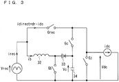
- Fig. 3 is the equivalent circuit of the direct AC power converter shown in Fig. 1 and Fig. 2 .
- the rectified voltage Vrec is expressed as a voltage source, and thus a switch Grec indicates whether the rectifying circuit 51 is conductive or not.
- the switches 31 and 41 are indicated by switches Gb and Gc, respectively.
- the regenerated current from the inverter 6 is not taken into consideration, and the diode of the switch 41 is not taken into consideration.
- the inverter 6 and its load are expressed as current sources for flowing a DC current idc into the inverter 6.
- the inverter 6 is operated by a so-called zero voltage vector in a state that a switch Gz is conductive.
- the inverter 6 short-circuits with respect to an inductive load with any one of the power supply lines L1 and L2, and thus does not receive an electric current from the DC link 7.
- the inverter 6 is allowed to be operated by any vectors other than the zero voltage vector when the inverter 6 receives an electric current from the DC link 7. Therefore, the inverter 6 is operated by any vectors other than the zero voltage vector when the switch Gz is non-conductive.
- the zero voltage duty dz is a time ratio corresponding to a period during which the inverter 6 adopts the zero voltage vector regardless of a magnitude of a voltage to be output. Further, the discharge duty dc is a time ratio of the conductivity of the switch 41.
- the rectifying duty dr is a time ratio of the conductivity of the rectifying circuit 51, and it is found from the formula (1) that it takes a value obtained by subtracting a sum of the discharge duty dc and the zero voltage duty dz from 1.
- Vdc dr ⁇ Vrec + dc ⁇ Vc
- the virtual DC link voltage Vdc is expressed by a sum of a product (dc•Vc) of the discharge duty dc and the capacitor voltage Vc, and a product (dr•Vrec) of the rectifying duty dr and the rectified voltage Vrec.
- This can be understood as an average of maximum values of voltages capable of being output from the inverter 6 in a cycle of control of a switching operation on the switch 41 or the inverter 6.
- Fig. 3 shows the virtual DC link voltage Vdc as a voltage to be generated at both ends of a current source idc (this causes the DC current idc to flow) representing the inverter 6 and the load of the inverter 6.
- an electric current from the voltage source indicating the rectified voltage Vrec (in this application, "a rectified current") irec is understood as a sum of the electric current ib to flow in the inductor 32 (included in the boost chopper 3) and an electric current idirect to flow from the rectifying circuit 51 into the inverter 6 in the actual configuration.
- the rectified current irec is not directly indicated.
- the electric current idirect is an electric current that flows from the rectifying circuit 51 into the DC link 7
- the electric current ib is an electric current that flows from the rectifying circuit 52 into the boost chopper 3.
- the rectified current irec is output from the output terminal 51c, and a part of the rectified current irec to flow into the inductor 32 becomes the electric current ib.
- Non-Patent Document 1 a period during which the electric current ib is allowed to flow is excluded from a period (providing period) during which an electric power is provided from the capacitor 34 to the DC link 7. Furthermore, the providing period and a period during which the capacitor 34 receives the electric power from the DC link 7 (receiving period) are set alternately in each 1/4 of the cycle of the AC voltage Vin. For this reason, the virtual DC link voltage Vdc does not exceed 1/ ⁇ 2 times a crest value of the AC voltage.
- the capacitor 34 does not always perform the discharge, and is discharged at the discharge duty dc. Therefore, a period during which the capacitor 34 can be charged is included even in the providing period.
- the capacitor 34 is charged in the boost chopper 3 so that the capacitor 34 is supplemented with an electric power.
- the virtual DC link voltage Vdc can exceed 1/ ⁇ 2 times the crest value of the AC voltage Vin.
- the capacitor 34 can be charged.
- the period during which the capacitor 34 is charged can be set to be longer than a period in a conventional technique. For this reason, a peak value of the electric current ib to flow in the inductor 32 can be reduced to be lower comparing to the conventional technique.
- a case where the rectified current irec is larger than the electric current idirect is first considered.
- this is a case where a margin exist for flowing the electric current ib in the boost chopper 3, and a magnitude of the rectifying duty dr is not limited by the rectified current irec.
- a case where the virtual DC link voltage Vdc is made to be the rectified voltage Vrec or less is further considered as a first case.
- the rectifying duty dr and the zero voltage duty dz in the first case are determined by the following formula (4).
- the capacitor 34 is not discharged via the switch 41.
- dr Vdc / Vrec
- dz 1 ⁇ Vdc / Vrec
- the rectifying duty dr should be set to a ratio of the command value Vdc* to the rectified voltage Vrec (Vdc*/Vrec), and the zero voltage duty dz should be set to a value obtained by subtracting the ratio from 1 in order to make the virtual DC link voltage Vdc follow the command value Vdc* with the discharge duty dc being zero in the first case.
- the zero voltage duty dz also becomes minimum here. This is because in order to match the virtual DC link voltage Vdc with the command value Vdc* even when the discharge duty dc increases, the zero voltage duty dz has to be increased according to the formula (2).
- a case where the rectified current irec is larger than the electric current idirect and the virtual DC link voltage Vdc is larger than the rectified voltage Vrec is considered as a second case.
- the discharge from the capacitor 34 to the DC link 7 has to be performed. That is to say, the discharge duty dc is set positive.
- the virtual DC link voltage Vdc has to be the capacitor voltage Vc or less.
- the zero voltage duty dz that does not contribute to a rise in the virtual DC link voltage Vdc is necessary to be reduced in order to reduce the discharge duty dc so that the loss and the rated current are reduced.
- the DC current idc can be fed by the rectified current irec. Therefore, the zero voltage duty dz can be reduced to zero.
- the formula (2) can be deformed into the following formula (5).
- the rectifying duty dr should be set to a ratio (Vdc* - Vc)/(Vrec - Vc), and the discharge duty dc should be set to a value obtained by subtracting the ratio from 1.
- to set the rectifying duty dr in the above manner means to set the discharge duty dc for making the zero voltage duty dz minimum and to set its value to (1 - dr). This is because the zero voltage duty dz reduces to zero also in this case.
- the control of the each duty means to set the discharge duty dc for making the zero voltage duty dz minimum based on two viewpoints.
- the first viewpoint is whether the rectified current irec is larger than the electric current idirect or not, namely, whether a command value irec* of the rectified current irec is set to be larger than an electric current irect or not.
- the second viewpoint is whether the virtual DC link voltage Vdc is larger than the rectified voltage Vrec or not, namely, whether the command value Vdc* is larger than the rectified voltage Vrec or not.
- dr_max indicates the rectifying duty dr respectively expressed by the formula (4) in the first case and the formula (5) in the second case.
- this period becomes the providing period during which the discharge is performed from the capacitor 34 to the DC link 7 at the discharge duty dc. Not only the discharge but also the charge of the capacitor 34 is performed by flowing of the electric current ib according to the command value ib* expressed by the formula (6) at the providing period.
- a period corresponding to the second case is called “charge/discharge zone”.
- a period corresponding to the first case is called “charge zone” in this embodiment because not the discharge but only the charge of the capacitor 34 is performed.
- a publicly-known method can be employed for a switching operation to be performed by a switch Gb (switch 31) using the electric current ib flowing in the boost chopper 3 to charge the capacitor 34 to the capacitor voltage Vc.
- This method may adopt a so-called current discontinuous mode, or a critical mode, or a current continuous mode.
- a case where the rectified current irec is the electric current idirect or less is considered as a third case.
- the formula (3) it is a case where a margin of flowing the electric current ib cannot exit.
- the rectifying duty dr that takes a value smaller than dr_max is adopted under a condition of the formula (7), so that the formula (3) is made to hold under conditions where irec ⁇ 0, dr ⁇ 0, idc > 0, and ib ⁇ 0.
- the command value ib* of the electric current ib is set to 0 so that ib ⁇ 0 at all times. That is to say, at a period during which the formula (7) holds, the capacitor 34 is not charged, and the capacitor 34 is discharged by the discharge duty dc determined below. In this embodiment, therefore, the period during which the formula (7) holds is called "discharge zone".
- the rectifying duty dr is determined by using a command value irec* and the estimated value idc ⁇ according to the following formula (8) in consideration of the formula (7).
- dr irec ⁇ / idc ⁇
- the rectifying duty dr comes to be set to a ratio (irec*/idc ⁇ ) of the command value irec* to the estimated value idc ⁇ .
- the rectifying duty dr is set to a value set by the formula (8), and the capacitor voltage Vc is actually fixed. Therefore, parameters that can be selected for making a right side of the formula (9) equal to the given command value Vdc* are the zero voltage duty dz and the discharge duty dc.
- the discharge duty dc is determined according to the following formula (10) directly led from the formula (9).
- dc Vdc ⁇ ⁇ dr ⁇ Vrec / Vc
- the capacitor voltage Vc technically comes to reduce at the period during which the formula (7) holds ("discharge zone"). This is because the command value ib* is set to 0 as described above. However, appropriate setting of the command value irec* enables the discharge zone to be shorten to an extent where the reduction in the capacitor voltage Vc can be ignored.
- the rectifying duty dr is determined according to the formula (8). Further, the discharge duty dc and the zero voltage duty dz are uniquely determined according to the formulas (10) and (11), respectively.
- the zero voltage duty dz is not allowed to take a value not less than the value determined according to the formula (11), it is set to a minimum value thereof. That is to say, it can be grasped that the discharge duty dc for making the zero voltage duty dz minimum is set also in the discharge zone, similarly to the charge zone and the charge/discharge zone.
- control signals Sb, Sc, and Sg can be generated by using a publicly-known technique.
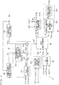
- Fig. 4 is a block diagram illustrating a configuration of the controller 9.
- the controller 9 is roughly divided into a current command generator 91, a DC current estimator 92, a duty divider 93, a pulse width modulation signal generator 94, and a chopper signal generator 95.
- the current command generator 91 generates the command value irec* of the rectified current irec.
- Fig. 4 illustrates a configuration where the command value irec* has an absolute value of a sinusoidal wave form, but the command value irec* is not always limited to provision of such a waveform.
- the DC current estimator 92 obtains the estimated value idc ⁇ of the DC current idc. As is understood from the equivalent circuit of Fig. 3 , a portion that can actually measure the DC current idc is not present in an actual circuit. Therefore, the estimated value idc ⁇ is adopted in the calculation expressed by the formulas (6) and (8).
- the DC current idc and the virtual DC link voltage Vdc enables obtaining of an electric power to be output from the inverter 6 in the equivalent circuit.
- an electric power to be output from the inverter 6 in the actual circuit is obtained by the three-phase electric current Iinv and a three-phase voltage Vinv to be output from the inverter 6. Therefore, theoretically the estimated value idc ⁇ can be obtained from the virtual DC link voltage Vdc, the electric current Iinv, and a voltage Vinv.
- the voltage Vinv to be output from the inverter 6 is controlled by the pulse width modulation signal generator 94 so as to follow its command value Vinv*.
- the virtual DC link voltage Vdc itself cannot be measured, but is controlled by the duty divider 93 so as to follow the command value Vdc*.
- the electric current Iinv can be measured from wire connection between the inverter 6 and the permanent-magnet synchronous motor PMSM. In this embodiment, therefore, the estimated value idc ⁇ is obtained from the command values Vdc* and Vinv*, and the electric current Iinv. Naturally, the estimated value idc ⁇ may be obtained by another method.
- the duty divider 93 determines the rectifying duty dr, the zero voltage duty dz, the discharge duty dc, and the command value ib* according to the methods described in the first to third cases based on the command values Vdc* and irec*, the capacitor voltage Vc, the rectified voltage Vrec, and the estimated value idc ⁇ .
- the expression "duty 'divider'" is given here because as expressed by the formula (2), the value 1 is divided by the rectifying duty dr, the zero voltage duty dz, and the discharge duty dc.
- the pulse width modulation signal generator 94 generates the control signals Sc and Sg based on the rectifying duty dr, the zero voltage duty dz, the discharge duty dc, and the command value Vinv* and Vdc*. For example, these duties and respective phase parts of the command value Vinv* are operated so that signal waves are generated, and the signal waves and a triangular wave carrier are compared with each other so that the control signals Sc and Sg can be generated. Since such a method is publicly known, and is described in, for example, Patent Documents 1 and 2, detailed description thereof is omitted.
- the chopper signal generator 95 has a boost chopper duty arithmetic unit 951 and a pulse width modulation signal generator 952.
- the boost chopper duty arithmetic unit 951 determines the boost duty db based on the command value ib*, the capacitor voltage Vc, and the rectified voltage Vrec.
- a method for determining the boost duty db varies depending on a mode that operates the boost chopper 3. As this method, however, a normal method for determining the discharge duty of the boost chopper can be adopted, and thus detailed description thereof is omitted.
- the pulse width modulation signal generator 952 can also generate the control signal Sb based on the boost duty db according to a publicly-known modulation method.
- the current command generator 91 has an output power estimator 911, a trigonometric function value generator 912, a capacitor voltage controller 913, an adder 914, a multiplier 915, and a divider 916.
- the output power estimator 911 obtains an estimated value Pout ⁇ of an output power Pout based on the command value Vinv* and the electric current Iinv. Since the DC current estimator 92 obtains the estimated value idc ⁇ in the above manner, the DC current estimator 92 may receive the estimated value Pout ⁇ obtained from the output power estimator 911 and the command value Vdc* so as to obtain the estimated value idc ⁇ .
- the capacitor voltage controller 913 obtains a deviation Vc*-Vc, which is output to the adder 914 after being provided with at least proportional control, between the capacitor voltage Vc and its command value Vc*.
- the adder 914 adds an output from the capacitor voltage controller 913 to the estimated value Pout ⁇ . This is a process for suitably setting a command value Pin* of the input power by correcting the estimated value Pout ⁇ so as to be larger/smaller when the capacitor voltage Vc becomes smaller/larger than the command value Vc* respectively, so as to reduce the deviation.
- the capacitor voltage controller 913 not merely proportional control as it is but proportional-integral control, or proportional-integral-derivative control is desirably adopted for stability of the deviation.
- the trigonometric function value generator 912 generates the trigonometric function value 2•sin 2 ⁇ based on a phase angle ⁇ of the power-supply voltage.
- the multiplier 915 multiplies an added result of the adder 914 and trigonometric function value 2•sin 2 ⁇ so as to obtain the command value Pin*.
- the command value irec* of the rectified current irec is obtained by dividing the command value Pin* by the rectified voltage Vrec.
- the phase angle ⁇ is estimated from, for example, the measured voltage Vin by a power-supply phase estimator 96.
- the power-supply phase estimator 96 can be constituted by, for example, a phase locked loop.
- the rectified voltage Vrec can be obtained in, for example such a manner that an absolute value circuit 97 obtains an absolute value of the measured voltage Vin. Since concrete configurations of the power-supply phase estimator 96 and the absolute value circuit 97 are publicly-known techniques, details thereof are not described.
- Fig. 5 is a flowchart organizing steps of obtaining the rectifying duty dr, the zero voltage duty dz, the discharge duty dc, and the command value ib*. It is grasped that this flowchart shows an operation of the duty divider 93.
- Step S101 corresponds to a determination whether the operation of the direct AC power converter corresponds to the first case or the second case if it does not correspond to the third case.
- the determination is made at step S101 whether the command value Vdc* of the virtual DC link voltage Vdc is the rectified voltage Vrec or less.
- the process goes to steps S102 and S104 when the determination is affirmative, steps S103 and S105 when negative, respectively.
- Steps S102 and S104 are processes for determining whether the operation of the direct AC power converter corresponds to the first case or the third case.
- dr_max Vdc*/Vrec is obtained at step S102.
- the determination at step S104 is affirmative, the operation of the direct AC power converter corresponds to the first case, and the process goes to steps S106 and S109.
- the determination at step S104 is negative, the operation of the direct AC power converter corresponds to the third case, and the process goes to steps S108 and S110.
- Steps S103 and S105 are processes for determining whether the operation of the direct AC power converter corresponds to the second case or the third case.
- dr_max (Vdc* - Vc)/(Vrec - Vc) is obtained at step S103.
- the determination at step S105 is affirmative, the operation of the direct AC power converter corresponds to the second case, and the process goes to steps S107 and S109.
- the determination at step S105 is negative, the operation of the direct AC power converter corresponds to the third case, and the process goes to steps S108 and S110.
- Steps S106, S107 and S108 are setting each duty according to the first case, the second case, and the third case, respectively.
- the step S109 is setting of the command value ib* according to the first case and the second case
- step S110 is setting of the command value ib* according to the third case.
- step S107 the discharge duty dc takes a value (1 - dr).
- the rectifying duty dr is expressed by the formula (5), and is smaller than 1. In this case, therefore, the discharge duty dc is larger than 0.
- step S108 when step S108 is executed, the discharge duty dc takes a value expressed by the formula (10).
- Vdc > Vrec a numerator of a right side of the formula (10) is larger than 0 regardless of the value of the rectifying duty dr. Also in this case, therefore, the discharge duty dc is larger than 0.
- the controller 9 can be realized by including, for example, a microcomputer and a storage device.
- the microcomputer executes the respective processing steps (in other words, the procedure) described in a program.
- the storage device can be configured by, for example, one of or a plurality of various storage devices such as a ROM (Read Only Memory), a RAM (Random Access Memory), rewritable non-volatile memory (such as an Erasable Programmable ROM (EPROM)), and a hard disc device.
- the storage device stores various information and data etc., and stores a program to be executed by the microcomputer, and provides a work area for executing the program.
- the microcomputer can be grasped to function as various means corresponding to the respective processing steps described in the program, or can be grasped to realize various functions corresponding to the respective processing steps.
- the controller 9 is not limited to this, and thus some of or entire of various procedures (obtaining respective measured values, executing steps S101 to S110 etc.) to be executed by the controller 9, or respective elements composing those, or various functions may be realized by hardware.
- a peak current of the electric current ib can be reduced to be lower than the peak current in a case where it is not allowed. This is because a change in the electric current ib at the receiving period should be reduced.
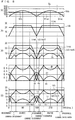
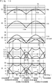
- Fig. 6 and Fig. 7 are graphs showing waveforms of specifications in a case where the peak current of the electric current ib is reduced while the above conditions (i) and (ii) are maintained by simulation ("comparative example 1"). It is noted that the virtual DC link voltage Vdc is set to 1/ ⁇ 2 (212 V) of a crest value (300 V) of the rectified voltage Vrec. Further, the capacitor voltage Vc is higher than the rectified voltage Vrec and is constant (400 V) (the same shall apply hereafter).
- the providing period and the receiving period are not adopted but “charge” and “discharge” are described on a horizontal axis.
- discharge means the period during which the capacitor 34 can be charged
- discharge means the period during which the capacitor 34 can be discharged.
- the electric current ib does not flow at the “discharge” period according to the above condition (i).
- charge and “discharge” are 1/4 (90°) of the cycle of the AC voltage Vin according to the condition (ii).
- a first row in Fig. 6 shows waveforms of the capacitor voltage Vc, the rectified voltage Vrec, and the virtual DC link voltage Vdc (this is assumed to accurately follow the command value Vdc*. The same shall apply hereafter).
- a second row in Fig. 6 shows waveforms of the rectified current irec (this is assumed to accurately follow the command value irec*. The same shall apply hereafter), and the DC current idc (this is assumed to be accurately estimated by the estimated value idc ⁇ . The same shall apply hereafter).
- the DC current idc is made to be constant, in cooperation with the virtual DC link voltage Vdc that takes a constant value, the output power Pout becomes constant.
- a third row in Fig. 6 shows waveforms of the rectified current irec, the electric current idirect (this is obtained by a product of the rectifying duty dr and the estimated value idc ⁇ . The same shall apply hereafter.), and the electric current ib (this is assumed to accurately follow the command value ib*. The same shall apply hereafter).
- a fourth row in Fig. 6 shows waveforms of the rectifying duty dr, the discharge duty dc, and the zero voltage duty dz.
- a fifth row in Fig. 6 shows waveforms of the DC current idc, the electric current idirect, an electric current ic to flow from the capacitor 34 to the DC link 7 (this is obtained by a product of the discharge duty dc and the estimated value idc ⁇ . The same shall apply hereafter.), a zero-phase current iz (this is obtained by a product of the zero voltage duty dz and the estimated value idc ⁇ . The same shall apply hereafter).
- a first row in Fig. 7 shows waveforms of an electric power Pout to be output from the inverter 6 (this is assumed to be accurately estimated based on the estimated value Pout ⁇ . The same shall apply hereafter.), an electric power Pdirect to be determined based on the rectified voltage Vrec and the electric current idirect, an electric power Pco to be discharged from the capacitor 34, and an electric power Pc to be input/output into/from the capacitor 34.
- the electric power Pc takes a negative value because it reduces the electric power Pout is reduced at a charge time, and it matches with the electric power Pco at a discharge time.
- a second row in Fig. 7 shows waveforms of the input power Pin (this is assumed to accurately follw the command value Pin*. The same shall apply hereafter.), the electric power Pdirect, an electric power Pci with which the capacitor 34 is charged, and the electric power Pc.
- the electric power Pc has the same absolute value as that of the electric power Pci at the charge time.
- a third row in Fig. 7 shows a graph where the electric powers Pc, Pci, and Pco relating to the capacitor 34 are extracted from the first and second rows in Fig. 7 so as to be brought together.
- the rectified current irec is planarized at the "charge" period, and is considerably distorted from the sinusoidal waveform.
- a power current abruptly changes, thus it may be said that the waveform is not practically preferable from a viewpoint of a power-supply noise and resonance of a filter circuit.
- the abrupt change in the power current is suppressed, namely, when the rectified current irec, which changes continuously and whose value becomes 0 when a power voltage crosses zero, is made to flow, the peak value of the electric current ib becomes larger.
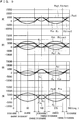
- Fig. 8 and Fig. 9 are graphs showing waveforms of specifications in a case where control is made by simulation according to the method of this embodiment ("example 1").
- Fig. 8 and Fig. 9 show waveforms of the specifications corresponding to Fig. 6 and Fig. 7 respectively.
- the virtual DC link voltage Vdc and the electric current idc are equal to those described with Fig. 6 and Fig. 7 , and are set to 212 V and 21.2 A, respectively.
- the crest value of the rectified voltage Vrec is also set to 300 V.
- the "discharge” period is a period during which the virtual DC link voltage Vdc is larger than the rectified voltage Vrec, iz > 0 (namely, dz > 0), and steps S108 and S110 in Fig. 5 are executed.
- the “charge/discharge” period includes a period during which the electric power Pci for charging the capacitor 34 is larger than the electric power Pco to be discharged from the capacitor 34 (namely, the period during which Pc ⁇ 0: this is adjacent to the "charge” period, and is separated from the “discharge” period), and a period during which the electric power Pco to be discharged from the capacitor 34 is larger than the electric power Pci for charging the capacitor 34 (namely, the period during which Pc > 0: this is adjacent to the "discharge” period and is separated from the “charge” period).
- the peak value is 40% (10.0 A) of the crest value of the electric current to flow from the single-phase AC power supply.
- the provision of the "charge/discharge" period enables the peak of the electric current ib to be reduced so as to be lower than that in the comparative
- Fig. 10 and Fig. 11 are graphs showing waveforms of specifications in a case where the control is made by simulation according to the method in this embodiment ("example 2"). Waveforms of the specifications corresponding to Fig. 8 and Fig. 9 are respectively shown. It is noted that a case is shown where the crest value of the rectified voltage Vrec is set to 300 V similarly to Fig. 6 to Fig. 9 , but the virtual DC link voltage Vdc is set to 0.8 (240 V) times the crest value of the rectified voltage Vrec.
- a ratio of the virtual DC link voltage Vdc to the crest value of the rectified voltage Vrec is heightened.
- the “charge” period correspond to steps S106 and S109 in Fig. 5
- the “discharge” period corresponds to steps S108 and S110 in Fig. 5
- the “charge/discharge” period corresponds to steps S107 and S109 in Fig. 5 .
- the crest value of the input current is 27.0 A
- the electric current ib is 12.0 A.
- Fig. 12 and Fig. 13 are graphs showing waveforms of specifications in a case where the peak current of the electric current ib is reduced by simulation without providing the "charge/discharge" period ("comparative example 2"). Waveforms of specifications corresponding to Fig. 6 and Fig. 7 are respectively shown. It is noted that the crest value of the rectified voltage Vrec is set to 300 V similarly to Fig.10 and Fig. 11 , and the virtual DC link voltage Vdc is set to 0.8 (240 V) times the crest value of the rectified voltage Vrec.
- the ratio of the virtual DC link voltage Vdc to the crest value of the rectified voltage Vrec is heightened.
- the peak value of the electric current ib naturally rises.
- the peak value of the electric current ib comes to 15.3 A
- the crest value of the input current comes to 30.3 A.
- the rectified current irec can show the sinusoidal waveform.
- Fig. 14 and Fig. 15 are graphs showing waveforms of specifications in a case where the control is made by simulation according to the method in this embodiment ("example 3"). Waveforms of specifications corresponding to Fig. 10 and Fig. 11 are respectively shown. It is noted that a case is shown where the crest value of the rectified voltage Vrec is set to 300 V similarly to Fig. 10 and Fig. 11 , the virtual DC link voltage Vdc is set to 0.8 (240 V) times the crest value of the rectified voltage Vrec, and further the waveform of the rectified current irec is the absolute value of the sinusoidal wave.
- the peak value of the electric current ib comes to 15.0 A and is still smaller than the comparative example 2. Furthermore, since the waveform of the rectified current irec is the absolute value of the sinusoidal wave, generation of so-called power line harmonics is suppressed. Such an effect of the example 3 cannot be realized as long as the condition (i) is maintained even if the condition (ii) is removed.
- Fig. 16 and Fig. 17 are graphs showing waveforms of specifications in a case where the control is made by simulation according to the method in this embodiment ("example 4"). Waveforms of specifications corresponding to Fig. 10 and Fig. 11 are respectively shown. It is noted that a case is shown where the crest value of the rectified voltage Vrec is set to 300 V similarly to Fig. 10 to Fig. 11 , the virtual DC link voltage Vdc is made to be equal to the crest value of the rectified voltage Vrec, and further the waveform of the rectified current irec is the absolute value of the sinusoidal wave.
- step S106 is executed as shown in the flowchart of Fig. 5 .
- step S106 is executed as shown in the flowchart of Fig. 5 .
- step S106 is executed as shown in the flowchart of Fig. 5 .
- the formula (1) holds, dr ⁇ 1.
- the control using the method in this embodiment enables the peak value of the electric current ib to flow in the direct AC power converter to be reduced. This contributes to reductions of the loss in the boost chopper 3, and a rated current of the inductor 32.
- the virtual DC link voltage Vdc can be set to 1/ ⁇ 2 or more times the crest value of the rectified voltage Vrec.
- the waveform of the rectified current irec can be the absolute value of the sinusoidal wave. This contributes to the suppression of the power line harmonics.
Landscapes
- Engineering & Computer Science (AREA)
- Power Engineering (AREA)
- Inverter Devices (AREA)
- Dc-Dc Converters (AREA)
- Rectifiers (AREA)
- Elevator Control (AREA)
- Control Of Ac Motors In General (AREA)
Claims (10)
- Direktwechselstromwandler, umfassend:einen Gleichstromzwischenkreis (7), der eine erste Stromversorgungsleitung (L1) und eine zweite Stromversorgungsleitung (L2) aufweist, wobei an die zweite Stromversorgungsleitung (L2) ein elektrisches Potential angelegt wird, das niedriger ist als ein elektrisches Potential der ersten Stromversorgungsleitung (L1);eine erste Gleichrichterschaltung (5, 51), die eine Vielzahl von Eingangsanschlüssen aufweist, die konfiguriert sind, um eine Wechselspannung (Vin) einzugeben, und ein Paar von Ausgangsanschlüssen (51c, 51d), von denen jeder mit dem Gleichstromzwischenkreis verbunden ist, die konfiguriert sind, um eine gleichgerichtete Spannung (Vrec) der Wechselspannung ausgeben;einen Wechselrichter (6), der konfiguriert ist, um eine Spannung, die am Gleichstromzwischenkreis (7) anliegt, in eine andere Wechselspannung umzurichten; undeinen Boost-Chopper (3), der an einer Ausgangsstufe einen Kondensator (34) aufweist;einen Schalter (41), der konfiguriert ist, um Entladung und Nicht-Entladung vom Kondensator (34) zum Gleichstromzwischenkreis zu schalten, wobeiein Nullspannungsbetrieb (dz) als ein Zeitverhältnis definiert ist, das einer Periode entspricht, in der der Wechselrichter (6) konfiguriert ist, um einen Nullspannungsvektor ungeachtet der Größe der auszugebenden Spannung anzupassen,ein Entladungsbetrieb (dc) als ein Zeitverhältnis einer Leitfähigkeit des Schalters (41) definiert ist, das konfiguriert ist, um eine Spannung (Vc) zwischen beiden Enden des Kondensators (34) an den Gleichstromzwischenkreis anzulegen, undein Gleichrichterbetrieb (dr) als ein Zeitverhältnis der Leitfähigkeit der Gleichrichterschaltung (51) definiert und konfiguriert ist, um einen Wert anzunehmen, der durch Subtrahieren einer Summe des Entladungsbetriebs (dc) und des Nullspannungsbetriebs (dz) von einem Wert 1 erhalten wird,dadurch gekennzeichnet, dassder Boost-Chopper (3) konfiguriert ist, um Laden in den Kondensator (34) mindestens in einer ersten Periode durchzuführen, die Teil einer Periode ist, in der der Entladungsbetrieb (dc) größer als 0 ist, wenn die Spannung (Vc) zwischen beiden Enden des Kondensators (34) größer ist als die gleichgerichtete Spannung.
- Direktwechselstromwandler nach Anspruch 1, wobei der Kondensator (34) konfiguriert ist, um in der ersten Periode und einem Teil oder einer Gesamtheit der Periode, während der der Entladungsbetrieb (dc) 0 beträgt, im Boost-Chopper (3) geladen wird.
- Direktwechselstromwandler nach Anspruch 2, wobei
der Kondensator (34) konfiguriert ist, um in der ersten Periode mit einem Ladestrom (Pci) geladen und mit einem Entladestrom (Pco) entladen zu werden, und
die erste Periode eine Periode aufweist, in der der Ladestrom größer ist als der Entladestrom, und eine Periode, in der der Entladestrom größer ist als der Ladestrom. - Direktwechselstromwandler nach einem der Ansprüche 1 bis 3, wobei eine virtuelle Gleichstromzwischenkreisspannung (Vdc), die durch eine Summe aus einem Produkt (dc·Vc) des Entladungsbetriebs (dc) und der Spannung (Vc) zwischen beiden Enden des Kondensators (34), und einem Produkt (dr·Vrec) des Gleichrichterbetriebs (dr) und der gleichgerichteten Spannung (Vrec) der Wechselspannung dargestellt wird, größer als das 1/√2-Fache der gleichgerichteten Spannung ist.
- Direktwechselstromwandler nach Anspruch 4, wobei
der Entladungsbetrieb (dc), der den Nullspannungsbetrieb (dz) minimal macht, auf Basis eines Sollwerts (irec*) eines gleichgerichteten Stroms (irec), bei dem es sich um eine Summe aus einem elektrischen Strom (ib), der im Boost-Chopper (3) fließt, und einem elektrischen Strom (idirect) handelt, der von der ersten Gleichrichterschaltung (5, 51) zum Wechselrichter (6) fließt, eines Sollwerts (Vdc*) der virtuellen Gleichstromzwischenkreisspannung (Vdc), der Spannung (Vc) zwischen beiden Enden des Kondensators (34), der gleichgerichteten Spannung (Vrec) und einem elektrischen Strom (idc), der in den Wechselrichter (6) eingegeben werden soll, eingestellt wird. - Direktwechselstromwandler nach Anspruch 5, wobei
der Gleichrichterbetrieb (dr) einen zweiten vorbestimmten Wert (dr_max) annimmt, und der Entladungsbetrieb (dc) einen Wert annimmt, der durch Subtrahieren des zweiten vorbestimmten Wertes von 1 erhalten wird, wenn die virtuelle Gleichstromzwischenkreisspannung (Vdc) größer ist als die gleichgerichtete Spannung (Vrec) und der Sollwert (irec*) des gleichgerichteten Stroms (irec) ein vorbestimmter Wert (dr_max∗idc^) oder mehr ist, wobei
es sich bei dem zweiten vorbestimmten Wert um einen Wert ((Vdc∗-Vc)/(Vrec-Vc)) handelt, der durch Dividieren eines Wertes, der durch Subtrahieren der Spannung (Vc) zwischen beiden Enden des Kondensators (34) vom Sollwert (Vdc*) einer virtuellen Gleichstromzwischenkreisspannung Vdc erhalten wird, durch einen Wert erhalten wird, der durch Subtrahieren der Spannung (Vc) zwischen beiden Enden des Kondensators (34) von der gleichgerichteten Spannung (Vrec) erhalten wird. - Direktwechselstromwandler nach Anspruch 1 oder Anspruch 2, weiter eine zweite Gleichrichterschaltung (52) umfassend, die konfiguriert ist, um die gleichgerichtete Spannung (Vrec) in den Boost-Chopper (3) einzugeben.
- Direktwechselstromwandler nach Anspruch 1 oder Anspruch 2, wobei das Paar von Ausgangsanschlüssen der ersten Gleichrichterschaltung mit einer Eingangsseite des Boost-Choppers (3) verbunden ist.
- Direktwechselstromwandler nach Anspruch 1, wobei der Entladungsbetrieb (dc) immer positiv ist.
- Direktwechselstromwandler nach Anspruch 1 oder Anspruch 2, weiter umfassend:
eine Diode, die mit dem Schalter (41) parallelgeschaltet ist, wobei die Diode dafür sorgt, dass es sich bei einer Laderichtung des Kondensators (34) vom Gleichstromzwischenkreis (7) um eine Vorwärtsrichtung handelt.
Applications Claiming Priority (2)
| Application Number | Priority Date | Filing Date | Title |
|---|---|---|---|
| JP2012214270 | 2012-09-27 | ||
| PCT/JP2013/076106 WO2014050987A1 (ja) | 2012-09-27 | 2013-09-26 | 直接形交流電力変換装置 |
Publications (3)
| Publication Number | Publication Date |
|---|---|
| EP2903148A1 EP2903148A1 (de) | 2015-08-05 |
| EP2903148A4 EP2903148A4 (de) | 2017-03-08 |
| EP2903148B1 true EP2903148B1 (de) | 2021-02-17 |
Family
ID=50388382
Family Applications (1)
| Application Number | Title | Priority Date | Filing Date |
|---|---|---|---|
| EP13842130.0A Active EP2903148B1 (de) | 2012-09-27 | 2013-09-26 | Direktwechselstromwandler |
Country Status (10)
| Country | Link |
|---|---|
| US (1) | US9698699B2 (de) |
| EP (1) | EP2903148B1 (de) |
| JP (1) | JP5626435B2 (de) |
| CN (1) | CN104662788B (de) |
| AU (1) | AU2013321021B2 (de) |
| BR (1) | BR112015006785B1 (de) |
| ES (1) | ES2856884T3 (de) |
| MY (1) | MY168637A (de) |
| SG (1) | SG10201704824RA (de) |
| WO (1) | WO2014050987A1 (de) |
Families Citing this family (23)
| Publication number | Priority date | Publication date | Assignee | Title |
|---|---|---|---|---|
| JP5804167B2 (ja) * | 2013-09-19 | 2015-11-04 | ダイキン工業株式会社 | 電力変換装置 |
| JP5664733B1 (ja) * | 2013-09-24 | 2015-02-04 | ダイキン工業株式会社 | 直接形電力変換装置の制御方法 |
| BR112016030924B1 (pt) * | 2014-07-18 | 2022-05-24 | Daikin Industries, Ltd | Conversor de potência ca direto |
| JP5930108B2 (ja) * | 2014-09-25 | 2016-06-08 | ダイキン工業株式会社 | 電力変換装置 |
| JP5874800B1 (ja) * | 2014-10-15 | 2016-03-02 | ダイキン工業株式会社 | 直接型電力変換器用制御装置 |
| JP5920520B1 (ja) * | 2014-12-17 | 2016-05-18 | ダイキン工業株式会社 | 充放電回路、充放電回路の制御方法、充放電回路の制御装置、及び直接形電力変換器 |
| JP6488685B2 (ja) * | 2014-12-17 | 2019-03-27 | ダイキン工業株式会社 | 電力変換装置 |
| CN104868809A (zh) * | 2015-05-29 | 2015-08-26 | 重庆瑜欣平瑞电子有限公司 | 一种数码发电机逆变器 |
| CN105356443B (zh) * | 2015-12-02 | 2019-04-23 | 浙江绿动电机科技有限公司 | 电动工具及其断电保护系统 |
| JP6103031B1 (ja) * | 2015-12-28 | 2017-03-29 | ダイキン工業株式会社 | 電力変換装置の制御装置 |
| JP6782410B2 (ja) * | 2016-01-28 | 2020-11-11 | 富士電機株式会社 | 電力変動緩和システム |
| JP6394741B1 (ja) * | 2017-05-30 | 2018-09-26 | ダイキン工業株式会社 | 電力変換装置、冷凍装置 |
| JP6418287B1 (ja) * | 2017-06-30 | 2018-11-07 | ダイキン工業株式会社 | 直接形電力変換器用制御装置 |
| CN108075673B (zh) * | 2017-09-19 | 2020-02-28 | 珠海格力电器股份有限公司 | 多路共地整流电路及开关电源 |
| US10689999B2 (en) * | 2018-02-22 | 2020-06-23 | Ge Aviation Systems, Llc | Power generation system |
| CN109842314B (zh) * | 2019-04-11 | 2025-01-14 | 广东美的制冷设备有限公司 | 驱动控制电路和家电设备 |
| CN109889072A (zh) * | 2019-04-11 | 2019-06-14 | 广东美的制冷设备有限公司 | 驱动控制电路和家电设备 |
| CN109980979B (zh) * | 2019-04-11 | 2021-01-05 | 广东美的制冷设备有限公司 | 运行控制方法、装置、电路、家电设备和计算机存储介质 |
| CN110022055B (zh) * | 2019-04-11 | 2021-03-02 | 广东美的制冷设备有限公司 | 运行控制方法、装置、电路、家电设备和计算机存储介质 |
| CN109889075B (zh) * | 2019-04-11 | 2025-01-07 | 广东美的制冷设备有限公司 | 驱动控制电路和家电设备 |
| JP7436783B2 (ja) * | 2019-09-30 | 2024-02-22 | ダイキン工業株式会社 | 電力変換装置 |
| WO2022176015A1 (ja) * | 2021-02-16 | 2022-08-25 | 三菱電機株式会社 | 電力変換装置および空気調和機 |
| JP7464925B2 (ja) * | 2022-02-28 | 2024-04-10 | 矢崎総業株式会社 | 充電器 |
Citations (1)
| Publication number | Priority date | Publication date | Assignee | Title |
|---|---|---|---|---|
| JP2011193678A (ja) * | 2010-03-16 | 2011-09-29 | Nagaoka Univ Of Technology | 単相/三相直接変換装置及びその制御方法 |
Family Cites Families (9)
| Publication number | Priority date | Publication date | Assignee | Title |
|---|---|---|---|---|
| US4437146A (en) * | 1982-08-09 | 1984-03-13 | Pacific Electro Dynamics, Inc. | Boost power supply having power factor correction circuit |
| US5235504A (en) * | 1991-03-15 | 1993-08-10 | Emerson Electric Co. | High power-factor converter for motor drives and power supplies |
| JP3496349B2 (ja) | 1995-07-19 | 2004-02-09 | 株式会社デンソー | 負荷駆動装置 |
| US6906503B2 (en) * | 2002-01-25 | 2005-06-14 | Precor Incorporated | Power supply controller for exercise equipment drive motor |
| JP4049189B2 (ja) * | 2006-04-24 | 2008-02-20 | ダイキン工業株式会社 | 直接形交流電力変換装置 |
| CN101499771B (zh) * | 2008-01-28 | 2013-03-06 | 王玉富 | 三相电源能量反馈三相电机变频调速驱动器 |
| JP4375489B1 (ja) * | 2008-06-27 | 2009-12-02 | ダイキン工業株式会社 | 電力変換装置 |
| JP2012105481A (ja) | 2010-11-11 | 2012-05-31 | Denso Corp | 電圧調整装置 |
| JP5381970B2 (ja) | 2010-12-24 | 2014-01-08 | ダイキン工業株式会社 | 制御信号生成装置、直接形電力変換装置並びに、その制御方法、その運転方法及びその設計方法 |
-
2013
- 2013-09-26 SG SG10201704824RA patent/SG10201704824RA/en unknown
- 2013-09-26 EP EP13842130.0A patent/EP2903148B1/de active Active
- 2013-09-26 BR BR112015006785-9A patent/BR112015006785B1/pt active IP Right Grant
- 2013-09-26 MY MYPI2015700992A patent/MY168637A/en unknown
- 2013-09-26 ES ES13842130T patent/ES2856884T3/es active Active
- 2013-09-26 AU AU2013321021A patent/AU2013321021B2/en active Active
- 2013-09-26 WO PCT/JP2013/076106 patent/WO2014050987A1/ja not_active Ceased
- 2013-09-26 US US14/431,691 patent/US9698699B2/en active Active
- 2013-09-26 CN CN201380050341.3A patent/CN104662788B/zh active Active
- 2013-09-26 JP JP2013199760A patent/JP5626435B2/ja active Active
Patent Citations (1)
| Publication number | Priority date | Publication date | Assignee | Title |
|---|---|---|---|---|
| JP2011193678A (ja) * | 2010-03-16 | 2011-09-29 | Nagaoka Univ Of Technology | 単相/三相直接変換装置及びその制御方法 |
Also Published As
| Publication number | Publication date |
|---|---|
| ES2856884T3 (es) | 2021-09-28 |
| MY168637A (en) | 2018-11-16 |
| BR112015006785A2 (pt) | 2017-07-04 |
| JP5626435B2 (ja) | 2014-11-19 |
| JP2014082926A (ja) | 2014-05-08 |
| US20150244282A1 (en) | 2015-08-27 |
| AU2013321021B2 (en) | 2015-12-24 |
| CN104662788B (zh) | 2017-05-24 |
| US9698699B2 (en) | 2017-07-04 |
| BR112015006785B1 (pt) | 2021-09-28 |
| EP2903148A1 (de) | 2015-08-05 |
| AU2013321021A1 (en) | 2015-05-14 |
| CN104662788A (zh) | 2015-05-27 |
| WO2014050987A1 (ja) | 2014-04-03 |
| EP2903148A4 (de) | 2017-03-08 |
| SG10201704824RA (en) | 2017-07-28 |
Similar Documents
| Publication | Publication Date | Title |
|---|---|---|
| EP2903148B1 (de) | Direktwechselstromwandler | |
| EP3171502B1 (de) | Direktwechselstromwandler | |
| EP3176935B1 (de) | Stromwandlungsvorrichtung | |
| CN102985281B (zh) | 用于电动车辆的充电装置 | |
| US10666143B2 (en) | Control device for direct power converter | |
| EP3048718A1 (de) | Stromwandler | |
| US11437921B2 (en) | Direct power converter and control device to improve an input power factor | |
| JP6103031B1 (ja) | 電力変換装置の制御装置 | |
| JP7436783B2 (ja) | 電力変換装置 | |
| JP6696626B2 (ja) | 電気またはハイブリッド車両の車載充電装置用の三相整流器を制御する方法 | |
| US10243498B2 (en) | Power converter control device | |
| CN113544961B (zh) | 直接型电力转换器用的控制装置 |
Legal Events
| Date | Code | Title | Description |
|---|---|---|---|
| PUAI | Public reference made under article 153(3) epc to a published international application that has entered the european phase |
Free format text: ORIGINAL CODE: 0009012 |
|
| 17P | Request for examination filed |
Effective date: 20150424 |
|
| AK | Designated contracting states |
Kind code of ref document: A1 Designated state(s): AL AT BE BG CH CY CZ DE DK EE ES FI FR GB GR HR HU IE IS IT LI LT LU LV MC MK MT NL NO PL PT RO RS SE SI SK SM TR |
|
| AX | Request for extension of the european patent |
Extension state: BA ME |
|
| DAX | Request for extension of the european patent (deleted) | ||
| RA4 | Supplementary search report drawn up and despatched (corrected) |
Effective date: 20170203 |
|
| RIC1 | Information provided on ipc code assigned before grant |
Ipc: H02M 1/42 20070101ALI20170130BHEP Ipc: H02M 7/48 20070101AFI20170130BHEP Ipc: H02M 7/12 20060101ALI20170130BHEP Ipc: H02M 5/458 20060101ALI20170130BHEP |
|
| STAA | Information on the status of an ep patent application or granted ep patent |
Free format text: STATUS: EXAMINATION IS IN PROGRESS |
|
| 17Q | First examination report despatched |
Effective date: 20181009 |
|
| GRAP | Despatch of communication of intention to grant a patent |
Free format text: ORIGINAL CODE: EPIDOSNIGR1 |
|
| STAA | Information on the status of an ep patent application or granted ep patent |
Free format text: STATUS: GRANT OF PATENT IS INTENDED |
|
| INTG | Intention to grant announced |
Effective date: 20200612 |
|
| GRAJ | Information related to disapproval of communication of intention to grant by the applicant or resumption of examination proceedings by the epo deleted |
Free format text: ORIGINAL CODE: EPIDOSDIGR1 |
|
| STAA | Information on the status of an ep patent application or granted ep patent |
Free format text: STATUS: EXAMINATION IS IN PROGRESS |
|
| GRAP | Despatch of communication of intention to grant a patent |
Free format text: ORIGINAL CODE: EPIDOSNIGR1 |
|
| STAA | Information on the status of an ep patent application or granted ep patent |
Free format text: STATUS: GRANT OF PATENT IS INTENDED |
|
| INTC | Intention to grant announced (deleted) | ||
| INTG | Intention to grant announced |
Effective date: 20201012 |
|
| GRAS | Grant fee paid |
Free format text: ORIGINAL CODE: EPIDOSNIGR3 |
|
| GRAA | (expected) grant |
Free format text: ORIGINAL CODE: 0009210 |
|
| STAA | Information on the status of an ep patent application or granted ep patent |
Free format text: STATUS: THE PATENT HAS BEEN GRANTED |
|
| AK | Designated contracting states |
Kind code of ref document: B1 Designated state(s): AL AT BE BG CH CY CZ DE DK EE ES FI FR GB GR HR HU IE IS IT LI LT LU LV MC MK MT NL NO PL PT RO RS SE SI SK SM TR |
|
| REG | Reference to a national code |
Ref country code: GB Ref legal event code: FG4D |
|
| REG | Reference to a national code |
Ref country code: CH Ref legal event code: EP |
|
| REG | Reference to a national code |
Ref country code: DE Ref legal event code: R096 Ref document number: 602013075737 Country of ref document: DE |
|
| REG | Reference to a national code |
Ref country code: AT Ref legal event code: REF Ref document number: 1362816 Country of ref document: AT Kind code of ref document: T Effective date: 20210315 |
|
| REG | Reference to a national code |
Ref country code: IE Ref legal event code: FG4D |
|
| REG | Reference to a national code |
Ref country code: LT Ref legal event code: MG9D |
|
| REG | Reference to a national code |
Ref country code: NL Ref legal event code: MP Effective date: 20210217 |
|
| PG25 | Lapsed in a contracting state [announced via postgrant information from national office to epo] |
Ref country code: HR Free format text: LAPSE BECAUSE OF FAILURE TO SUBMIT A TRANSLATION OF THE DESCRIPTION OR TO PAY THE FEE WITHIN THE PRESCRIBED TIME-LIMIT Effective date: 20210217 Ref country code: FI Free format text: LAPSE BECAUSE OF FAILURE TO SUBMIT A TRANSLATION OF THE DESCRIPTION OR TO PAY THE FEE WITHIN THE PRESCRIBED TIME-LIMIT Effective date: 20210217 Ref country code: GR Free format text: LAPSE BECAUSE OF FAILURE TO SUBMIT A TRANSLATION OF THE DESCRIPTION OR TO PAY THE FEE WITHIN THE PRESCRIBED TIME-LIMIT Effective date: 20210518 Ref country code: LT Free format text: LAPSE BECAUSE OF FAILURE TO SUBMIT A TRANSLATION OF THE DESCRIPTION OR TO PAY THE FEE WITHIN THE PRESCRIBED TIME-LIMIT Effective date: 20210217 Ref country code: PT Free format text: LAPSE BECAUSE OF FAILURE TO SUBMIT A TRANSLATION OF THE DESCRIPTION OR TO PAY THE FEE WITHIN THE PRESCRIBED TIME-LIMIT Effective date: 20210617 Ref country code: BG Free format text: LAPSE BECAUSE OF FAILURE TO SUBMIT A TRANSLATION OF THE DESCRIPTION OR TO PAY THE FEE WITHIN THE PRESCRIBED TIME-LIMIT Effective date: 20210517 Ref country code: NO Free format text: LAPSE BECAUSE OF FAILURE TO SUBMIT A TRANSLATION OF THE DESCRIPTION OR TO PAY THE FEE WITHIN THE PRESCRIBED TIME-LIMIT Effective date: 20210517 |
|
| REG | Reference to a national code |
Ref country code: AT Ref legal event code: MK05 Ref document number: 1362816 Country of ref document: AT Kind code of ref document: T Effective date: 20210217 |
|
| PG25 | Lapsed in a contracting state [announced via postgrant information from national office to epo] |
Ref country code: SE Free format text: LAPSE BECAUSE OF FAILURE TO SUBMIT A TRANSLATION OF THE DESCRIPTION OR TO PAY THE FEE WITHIN THE PRESCRIBED TIME-LIMIT Effective date: 20210217 Ref country code: RS Free format text: LAPSE BECAUSE OF FAILURE TO SUBMIT A TRANSLATION OF THE DESCRIPTION OR TO PAY THE FEE WITHIN THE PRESCRIBED TIME-LIMIT Effective date: 20210217 Ref country code: LV Free format text: LAPSE BECAUSE OF FAILURE TO SUBMIT A TRANSLATION OF THE DESCRIPTION OR TO PAY THE FEE WITHIN THE PRESCRIBED TIME-LIMIT Effective date: 20210217 Ref country code: NL Free format text: LAPSE BECAUSE OF FAILURE TO SUBMIT A TRANSLATION OF THE DESCRIPTION OR TO PAY THE FEE WITHIN THE PRESCRIBED TIME-LIMIT Effective date: 20210217 Ref country code: PL Free format text: LAPSE BECAUSE OF FAILURE TO SUBMIT A TRANSLATION OF THE DESCRIPTION OR TO PAY THE FEE WITHIN THE PRESCRIBED TIME-LIMIT Effective date: 20210217 |
|
| REG | Reference to a national code |
Ref country code: ES Ref legal event code: FG2A Ref document number: 2856884 Country of ref document: ES Kind code of ref document: T3 Effective date: 20210928 |
|
| PG25 | Lapsed in a contracting state [announced via postgrant information from national office to epo] |
Ref country code: IS Free format text: LAPSE BECAUSE OF FAILURE TO SUBMIT A TRANSLATION OF THE DESCRIPTION OR TO PAY THE FEE WITHIN THE PRESCRIBED TIME-LIMIT Effective date: 20210617 |
|
| PG25 | Lapsed in a contracting state [announced via postgrant information from national office to epo] |
Ref country code: SM Free format text: LAPSE BECAUSE OF FAILURE TO SUBMIT A TRANSLATION OF THE DESCRIPTION OR TO PAY THE FEE WITHIN THE PRESCRIBED TIME-LIMIT Effective date: 20210217 Ref country code: CZ Free format text: LAPSE BECAUSE OF FAILURE TO SUBMIT A TRANSLATION OF THE DESCRIPTION OR TO PAY THE FEE WITHIN THE PRESCRIBED TIME-LIMIT Effective date: 20210217 Ref country code: EE Free format text: LAPSE BECAUSE OF FAILURE TO SUBMIT A TRANSLATION OF THE DESCRIPTION OR TO PAY THE FEE WITHIN THE PRESCRIBED TIME-LIMIT Effective date: 20210217 Ref country code: AT Free format text: LAPSE BECAUSE OF FAILURE TO SUBMIT A TRANSLATION OF THE DESCRIPTION OR TO PAY THE FEE WITHIN THE PRESCRIBED TIME-LIMIT Effective date: 20210217 |
|
| REG | Reference to a national code |
Ref country code: DE Ref legal event code: R097 Ref document number: 602013075737 Country of ref document: DE |
|
| PG25 | Lapsed in a contracting state [announced via postgrant information from national office to epo] |
Ref country code: DK Free format text: LAPSE BECAUSE OF FAILURE TO SUBMIT A TRANSLATION OF THE DESCRIPTION OR TO PAY THE FEE WITHIN THE PRESCRIBED TIME-LIMIT Effective date: 20210217 Ref country code: RO Free format text: LAPSE BECAUSE OF FAILURE TO SUBMIT A TRANSLATION OF THE DESCRIPTION OR TO PAY THE FEE WITHIN THE PRESCRIBED TIME-LIMIT Effective date: 20210217 Ref country code: SK Free format text: LAPSE BECAUSE OF FAILURE TO SUBMIT A TRANSLATION OF THE DESCRIPTION OR TO PAY THE FEE WITHIN THE PRESCRIBED TIME-LIMIT Effective date: 20210217 |
|
| PLBE | No opposition filed within time limit |
Free format text: ORIGINAL CODE: 0009261 |
|
| STAA | Information on the status of an ep patent application or granted ep patent |
Free format text: STATUS: NO OPPOSITION FILED WITHIN TIME LIMIT |
|
| 26N | No opposition filed |
Effective date: 20211118 |
|
| PG25 | Lapsed in a contracting state [announced via postgrant information from national office to epo] |
Ref country code: AL Free format text: LAPSE BECAUSE OF FAILURE TO SUBMIT A TRANSLATION OF THE DESCRIPTION OR TO PAY THE FEE WITHIN THE PRESCRIBED TIME-LIMIT Effective date: 20210217 |
|
| PG25 | Lapsed in a contracting state [announced via postgrant information from national office to epo] |
Ref country code: SI Free format text: LAPSE BECAUSE OF FAILURE TO SUBMIT A TRANSLATION OF THE DESCRIPTION OR TO PAY THE FEE WITHIN THE PRESCRIBED TIME-LIMIT Effective date: 20210217 |
|
| REG | Reference to a national code |
Ref country code: CH Ref legal event code: PL |
|
| REG | Reference to a national code |
Ref country code: BE Ref legal event code: MM Effective date: 20210930 |
|
| PG25 | Lapsed in a contracting state [announced via postgrant information from national office to epo] |
Ref country code: IS Free format text: LAPSE BECAUSE OF FAILURE TO SUBMIT A TRANSLATION OF THE DESCRIPTION OR TO PAY THE FEE WITHIN THE PRESCRIBED TIME-LIMIT Effective date: 20210617 Ref country code: MC Free format text: LAPSE BECAUSE OF FAILURE TO SUBMIT A TRANSLATION OF THE DESCRIPTION OR TO PAY THE FEE WITHIN THE PRESCRIBED TIME-LIMIT Effective date: 20210217 |
|
| PG25 | Lapsed in a contracting state [announced via postgrant information from national office to epo] |
Ref country code: LU Free format text: LAPSE BECAUSE OF NON-PAYMENT OF DUE FEES Effective date: 20210926 Ref country code: IE Free format text: LAPSE BECAUSE OF NON-PAYMENT OF DUE FEES Effective date: 20210926 Ref country code: BE Free format text: LAPSE BECAUSE OF NON-PAYMENT OF DUE FEES Effective date: 20210930 |
|
| PG25 | Lapsed in a contracting state [announced via postgrant information from national office to epo] |
Ref country code: LI Free format text: LAPSE BECAUSE OF NON-PAYMENT OF DUE FEES Effective date: 20210930 Ref country code: CH Free format text: LAPSE BECAUSE OF NON-PAYMENT OF DUE FEES Effective date: 20210930 |
|
| PG25 | Lapsed in a contracting state [announced via postgrant information from national office to epo] |
Ref country code: HU Free format text: LAPSE BECAUSE OF FAILURE TO SUBMIT A TRANSLATION OF THE DESCRIPTION OR TO PAY THE FEE WITHIN THE PRESCRIBED TIME-LIMIT; INVALID AB INITIO Effective date: 20130926 |
|
| PG25 | Lapsed in a contracting state [announced via postgrant information from national office to epo] |
Ref country code: CY Free format text: LAPSE BECAUSE OF FAILURE TO SUBMIT A TRANSLATION OF THE DESCRIPTION OR TO PAY THE FEE WITHIN THE PRESCRIBED TIME-LIMIT Effective date: 20210217 |
|
| P01 | Opt-out of the competence of the unified patent court (upc) registered |
Effective date: 20230525 |
|
| PG25 | Lapsed in a contracting state [announced via postgrant information from national office to epo] |
Ref country code: MK Free format text: LAPSE BECAUSE OF FAILURE TO SUBMIT A TRANSLATION OF THE DESCRIPTION OR TO PAY THE FEE WITHIN THE PRESCRIBED TIME-LIMIT Effective date: 20210217 |
|
| PG25 | Lapsed in a contracting state [announced via postgrant information from national office to epo] |
Ref country code: MT Free format text: LAPSE BECAUSE OF FAILURE TO SUBMIT A TRANSLATION OF THE DESCRIPTION OR TO PAY THE FEE WITHIN THE PRESCRIBED TIME-LIMIT Effective date: 20210217 |
|
| PGFP | Annual fee paid to national office [announced via postgrant information from national office to epo] |
Ref country code: DE Payment date: 20250730 Year of fee payment: 13 |
|
| PGFP | Annual fee paid to national office [announced via postgrant information from national office to epo] |
Ref country code: TR Payment date: 20250919 Year of fee payment: 13 Ref country code: IT Payment date: 20250825 Year of fee payment: 13 |
|
| PGFP | Annual fee paid to national office [announced via postgrant information from national office to epo] |
Ref country code: GB Payment date: 20250807 Year of fee payment: 13 |
|
| PGFP | Annual fee paid to national office [announced via postgrant information from national office to epo] |
Ref country code: FR Payment date: 20250808 Year of fee payment: 13 |
|
| PGFP | Annual fee paid to national office [announced via postgrant information from national office to epo] |
Ref country code: ES Payment date: 20251013 Year of fee payment: 13 |