EP2897141A1 - Induktiver Spannungswandler - Google Patents
Induktiver Spannungswandler Download PDFInfo
- Publication number
- EP2897141A1 EP2897141A1 EP14195813.2A EP14195813A EP2897141A1 EP 2897141 A1 EP2897141 A1 EP 2897141A1 EP 14195813 A EP14195813 A EP 14195813A EP 2897141 A1 EP2897141 A1 EP 2897141A1
- Authority
- EP
- European Patent Office
- Prior art keywords
- coil
- layers
- double
- voltage converter
- double layer
- Prior art date
- Legal status (The legal status is an assumption and is not a legal conclusion. Google has not performed a legal analysis and makes no representation as to the accuracy of the status listed.)
- Granted
Links
Images

Classifications
-
- H—ELECTRICITY
- H01—ELECTRIC ELEMENTS
- H01F—MAGNETS; INDUCTANCES; TRANSFORMERS; SELECTION OF MATERIALS FOR THEIR MAGNETIC PROPERTIES
- H01F27/00—Details of transformers or inductances, in general
- H01F27/28—Coils; Windings; Conductive connections
- H01F27/2823—Wires
-
- H—ELECTRICITY
- H01—ELECTRIC ELEMENTS
- H01F—MAGNETS; INDUCTANCES; TRANSFORMERS; SELECTION OF MATERIALS FOR THEIR MAGNETIC PROPERTIES
- H01F27/00—Details of transformers or inductances, in general
- H01F27/28—Coils; Windings; Conductive connections
- H01F27/32—Insulating of coils, windings, or parts thereof
- H01F27/323—Insulation between winding turns, between winding layers
-
- H—ELECTRICITY
- H01—ELECTRIC ELEMENTS
- H01F—MAGNETS; INDUCTANCES; TRANSFORMERS; SELECTION OF MATERIALS FOR THEIR MAGNETIC PROPERTIES
- H01F27/00—Details of transformers or inductances, in general
- H01F27/34—Special means for preventing or reducing unwanted electric or magnetic effects, e.g. no-load losses, reactive currents, harmonics, oscillations, leakage fields
Definitions
- the invention relates to inductive voltage transformers and in particular low and medium voltage converters.
- harmonics In the electrical energy supply networks, in particular in low and medium voltage networks (up to 1 kV or between 1 kV and 75 kV) occur more harmonics. These harmonics are mainly caused by regenerative generation plants and customers with frequency converters and adversely affect the so-called "power quality" or voltage quality of a power supply network. In order to ensure a desired voltage quality in a power supply network, it is first necessary to determine the actually existing voltage quality.
- Harmonics can be quantified by a THD (total harmonic distortion) value.
- the harmonic content or the THD value must be below 0.08 for an acceptable voltage quality in accordance with the applicable VDE and IEC regulations in low and medium voltage networks in the frequency range up to 2.5 kHz. In addition, it is recommended that the THD value in the frequency range between 2.5 kHz and 9 kHz does not exceed the limit of 0.002. Individual values also apply to the individual harmonics, which must be complied with. In order to check compliance with these limits, voltage converters with downstream measuring devices should preferably be used.
- the low and medium voltage from the power grid should be reduced so that designed for low voltages and therefore cost-effective measuring devices can be used to measure voltage or voltage waveforms in a low or medium voltage network. From the results of the measuring devices, which are arranged behind a voltage transformer, conclusions can be drawn on the conditions in the respective low- or medium-voltage network, in particular also with regard to the voltage quality.
- inductive voltage transformers are known as voltage transformers. These work on the principle of the transformer.
- corresponding voltage transformers basically have natural oscillations that are relevant for the harmonics in low and medium voltage networks Frequency range, which disturb the transmission in the voltage converter.
- a 20 kV inductive voltage converter according to the prior art have natural oscillations in the frequency range of 2 kHz to 15 kHz, the transmission ratio of the voltage converter from 1.5 kHz can be so strongly influenced that a measurement of the harmonics using a corresponding voltage converter is not possible.
- there is a limitation of the frequency band whereby only frequencies below 1.5 kHz can be transmitted acceptable.
- a determination of harmonics in a low or medium voltage network over 1.5 kHz is therefore not or only partially possible with an inductive voltage converter according to the prior art. The same applies to the verification of THD values in low and medium voltage networks.
- Object of the present invention is to provide a low-maintenance voltage converter, which is designed to transmit the harmonics in low or medium voltage networks so that the harmonics are detected with sufficient accuracy with a downstream measuring device for determining the voltage quality in the low or medium voltage network can.
- the invention relates to a voltage converter comprising a primary coil having a lower coil half and an upper coil half, at least one secondary coil and a coil core, wherein the at least one secondary coil around the coil core and the primary coil is arranged around the at least one secondary coil, wherein the windings of the primary coil as a plurality of double plies are made, and wherein the summed capacitance of the double plies of the lower coil half is greater than or equivalent to the summed capacitance of the double plies of the upper coil half.
- a “double layer” is a winding pair of a coil in which the two windings have an opposite winding sense.
- the one winding is wound in a first position starting from a winding start in a direction opposite to the spool core first direction.
- the coil wire goes from the first layer directly to a second layer which is wound in the direction opposite to the direction of the first layer.
- the second layer is thus wound so that the coil wire runs back from the end of the coil back to the beginning of the winding.
- the primary coil has windings in a plurality of double layers.
- the inner and thus the coil core next double layers form the "lower coil half", the adjoining outer and further away from the coil core double layers form the "upper coil half".
- the number of double layers in the lower and in the upper half of the coil are the same for an even total number of double layers.
- one of the two coil halves has a double layer more than the other.
- the center double layer may be left outside so that there are two coil halves with identical numbers of double layers and a single intermediate double layer.
- the two layers of a double layers can have a constant over the entire length of the coil distance from each other. But it is also possible that the distance between the two layers of a double layer in sections changes. A corresponding sectionally changing the distance between two layers is, for example, before at a segment winding. At least in the sense of the present invention, a segment winding is also a winding which is designed as a plurality of double layers, albeit with a non-constant spacing between the layers of a double layer.
- the invention is based on the finding that the inventive design of the primary coil of an inductive voltage converter, an advantageous, almost linear transmission behavior in a wide frequency range starting from and greater than 0 Hz can be achieved. In particular, a nearly linear transmission behavior over a wider frequency range compared to ordinary inductive voltage transformers can be achieved.
- the inventive design of the primary coil of an inductive voltage converter is namely achieved that shifts the zero of the first resonance behind the first pole. There is then a slight overcompensation, which results in a wide frequency range from 0 Hz, a nearly linear transmission behavior. In particular, the transmission behavior in said frequency range may have an error of less than 5%.
- the effective capacity of the double layers in the upper half of the coil is generally greater than the effective capacity of the double layers in the lower half of the coil due to the geometrical characteristics of a coil.
- C i is the capacitance of the i-th double layer of a coil with N double layers
- ⁇ i is the dielectric constant of the i-th double layer
- r i is the radius of the i-th double layer
- l i is the winding length of the i-th double layer
- d i den Describes the distance between the two layers of the i-th double layer.
- the effective capacity of the double layers in the upper coil half (C OSH ) is greater than the effective capacity of the double layers in the lower coil half (C USH ).
- the invention has recognized that by changing the ratio of the effective capacitance of the coil halves of the primary coil of an inductive voltage converter to C USH ⁇ C OSH has the desired advantageous transmission behavior of the voltage converter or the above-described overcompensation result.
- the inventive ratio of the effective capacitance of the coil halves of the primary coil, so that the summed capacitance of the double layers of the lower coil half is greater than or equivalent to the effective capacity of the double layers of the upper coil half, can be achieved by adjusting the capacitances of the individual double layers of the coils. While the radius of the individual double layers r i is practically predetermined by the geometric shape of the coil, in particular the dielectric constant ⁇ i and the distance d i between the two layers of the individual double layers can be adapted such that the desired ratio of the effective capacitances of the two coil halves is reached.
- the dielectric constant of the insulation is preferably as large as possible and / or the distance between the two layers of at least one double layer in the lower coil half selected as small as possible in at least one double layer of the lower coil half. It is further preferred if, in all double layers of the lower coil half, the dielectric constant of the insulation is as large as possible and / or the distance between the two layers of the double layers is selected to be as small as possible.
- the other technical boundary conditions should not be violated. For example, to avoid flashover, minimum thicknesses for a given insulation material must be maintained to ensure the necessary insulation.
- the dielectric constant of the insulation of at least one double-layer winding as close as possible to 1 and / or the distance between the two layers of at least one double layer in the upper coil half is preferably chosen to be as large as possible. It is further preferred if, in all double layers of the upper coil half, the dielectric constant of the insulation is selected as close as possible to 1 and / or the distance between the two layers of the double layers is as large as possible.
- the other technical boundary conditions should not be violated. Thus, for example, care must be taken that the field strengths in the region of the upper coil halves and / or the double-layer voltage of a double layer in the upper coil half do not exceed a maximum value dependent on the material of the coil.
- the desired ratio of the effective capacitances of the two coil halves can be achieved.
- the desired large distance between the two layers of a double layer in the upper coil half can preferably be achieved by two or more ply papers are inserted between the two layers of a double layer in the upper bobbin half. It can thus be easily reduced the capacity of a double layer in the upper bobbin half using the ply paper, which is also used in the lower bobbin half.
- the primary coil have a total of 67 double layers, wherein the inner double layers 1 to 33 - so the lower coil half - a simple insulation by one layer paper and the outer double layers 34 to 67 have a triple insulation with three ply papers ,
- the individual ply papers can each have the same thickness and in particular be of the same dielectric.
- a voltage converter according to the invention and in particular the primary coil, can have the same shape as an inductive voltage converter according to the prior art, despite the improved transmission behavior.
- This possible contour retention of the voltage converter is particularly advantageous in the exchange of inductive voltage transformers according to the prior art by voltage converters according to the invention.
- the primary coil and / or the at least one secondary coil are wound from enameled copper wire.
- the core is preferably made of thin iron sheets and / or of nanocrystalline or amorphous materials.
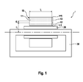
- FIG. 1 a first embodiment of an inductive voltage converter 1 according to the invention is shown.
- the voltage converter 1 comprises a primary coil 10, a secondary coil 20 and a coil core 30.
- the secondary coil 20 is arranged around the coil core 30, while the primary coil 10 is arranged around the secondary coil 20.
- the primary coil 10 has connections for connection to a power supply network.
- the secondary coil 20 has connections for connection to a measuring device. Because of
- Clarity are the mentioned connections and the measuring device in FIG. 1 not shown. It is also possible to provide more than one secondary coil 20, wherein the individual secondary coils 20 can then each be connected to different measuring devices.
- the windings of the primary coil 10 are designed as a plurality of double layers 11.
- N 6.
- the primary coil 10 is divided into a lower coil half 12 and an upper coil half 13, wherein the two coil halves 12, 13 each comprise the same number of double layers 11. According to the invention, it is provided that the effective capacity of the double layers 11 of the lower coil halves 12 is greater than, equal to or equivalent to the effective capacity of the double layers 11 of the upper coil half 13.
- C i ⁇ i ⁇ 2 ⁇ ⁇ ⁇ r i ⁇ l i d i
- i 1 . 2 ... N
- C i is the capacitance of the i-th double layer 11 of a coil with N double layers
- ⁇ i is the dielectric constant of the i-th double layer
- r i is the radius of the i-th double layer
- l i is the winding length of the i-th double layer
- d i describes the distance between the two layers of the i-th double layer.
- the quantities r i , d i and l i are in FIG. 1 illustrated by way of example for one of the double layers 11 of the primary coil.
- the distances d i in the double layer 11 of the upper bobbin half 13 are larger than in the double layer 11 of the lower bobbin half 12.
- the dielectric constant ⁇ i in the double layer 11 of the lower bobbin half 12 as large as possible, while 11 of the upper in the bilayers Spool half 13 is as close as possible to 1.
- FIG. 2 become the advantages of an inductive voltage converter 1 according to FIG. 1 compared to a conventional inductive voltage converter clearly.
- the primary coil is usually constructed, ie in particular the dielectric constant ⁇ i and the distance d i between the two layers of a double layer for each double layer of the coil is the same.
- phase response is also in a wide, starting from 0 Hz frequency range (up to 12 kHz) almost constant. Compared to a conventional voltage converter, however, the amplitude response up to a frequency of about 11 kHz is almost constant. Due to this advantageous transmission behavior of the voltage converter is according to FIG. 1 well suited for the determination of the voltage quality in a power supply network and in particular in a low or medium voltage network.
Landscapes
- Engineering & Computer Science (AREA)
- Power Engineering (AREA)
- Coils Of Transformers For General Uses (AREA)
Abstract
Description
- Die Erfindung betrifft induktive Spannungswandler und insbesondere Nieder- und Mittelspannungswandler.
- In den elektrischen Energieversorgungsnetzen, insbesondere in Nieder- und Mittelspannungsnetzen (bis 1 kV bzw. zwischen 1 kV und 75 kV) treten vermehrt Oberschwingungen auf. Diese Oberschwingungen werden vorwiegend von regenerativen Erzeugungsanlagen und Abnehmern mit Frequenzumrichtern verursacht und beeinträchtigen die sog. "Power Quality" bzw. Spannungsqualität eines Energieversorgungsnetzes negativ. Um eine gewünschte Spannungsqualität in einem Energieversorgungsnetz zu gewährleisten, ist es zunächst erforderlich, die tatsächlich vorhandene Spannungsqualität zu ermitteln.
- Oberschwingungen können durch einen THD-Wert ("Total harmonic distortion" bzw. "gesamte harmonische Verzerrung") quantifiziert werden. Der THD ist definiert als das Verhältnis des Effektivwertes der Summe aller Oberschwingungsanteile zum Effektivwert der Grundschwingung und lässt sich wie folgt berechnen:

- In dieser Berechnung bedeutet Un die Effektivwert-Spannung Ueff der harmonischen Oberschwingungen n mit n>1 bzw. der Grundschwingung n=1.
- Der Anteil an Oberschwingungen bzw. der THD-Wert muss für eine akzeptable Spannungsqualität gemäß den geltenden VDE- und IEC-Bestimmungen in Nieder- und Mittelspannungsnetzen im Frequenzbereich bis 2,5 kHz unter 0,08 liegen. Darüber hinaus wird empfohlen, dass der THD-Wert im Frequenzbereich zwischen 2,5 kHz und 9 kHz die Grenze von 0,002 nicht überschreitet. Es gelten für die einzelnen Oberschwingungen ebenfalls individuelle Werte, die eingehalten werden müssen. Um die Einhaltung dieser Grenzen zu überprüfen, sollen vorzugsweise Spannungswandler mit nachgeschalteten Messeinrichtungen zum Einsatz kommen.
- Mit Spannungswandlern soll die Nieder- und Mittelspannung aus dem Energieversorgungsnetz derart herabgesetzt werden, dass für niedrige Spannungen ausgelegte und damit kostengünstige Messeinrichtungen zum Einsatz kommen können, um Spannung oder Spannungsverläufe in einem Nieder- oder Mittelspannungsnetz zu messen. Aus den Ergebnissen der Messeinrichtungen, die hinter einem Spannungswandler angeordnet sind, lassen sich Rückschlüsse auf die Verhältnisse im jeweiligen Nieder- oder Mittelspannungsnetz ziehen, insbesondere auch hinsichtlich der Spannungsqualität.
- Grundsätzlich sind als Spannungswandler induktive Spannungswandler bekannt. Diese funktionieren nach dem Prinzip des Transformators. Entsprechende Spannungswandler besitzen jedoch grundsätzlich Eigenschwingungen im für die Oberschwingungen in Nieder- und Mittelspannungsnetzen relevanten Frequenzbereich, welche die Übertragung im Spannungswandler stören. So kann beispielsweise ein induktiver 20-kV-Spannungswandler gemäß dem Stand der Technik Eigenschwingungen im Frequenzbereich von 2 kHz bis 15 kHz aufweisen, wobei das Übersetzungsverhältnis des Spannungswandlers bereits ab 1,5 kHz so stark beeinflusst sein kann, dass eine Messung der Oberschwingungen mithilfe eines entsprechenden Spannungswandlers nicht möglich ist. Es kommt also im Prinzip zu einer Begrenzung des Frequenzbands, wodurch nur Frequenzen unter 1,5 kHz akzeptabel übertragen werden können. Eine Bestimmung von Oberschwingungen in einem Nieder- oder Mittelspannungsnetz über 1,5 kHz ist mit einem induktiven Spannungswandler gemäß dem Stand der Technik daher nicht oder nur eingeschränkt möglich. Für die Überprüfung der THD-Werte in Nieder- und Mittelspannungsnetzen gilt das Gleiche.
- Um Oberschwingungen in Nieder- oder Mittelspannungsnetzen ausreichend genau messen zu können, wird grundsätzlich gefordert, dass dafür vorgesehene Spannungswandler zumindest bis 2,5 kHz ein konstantes Übertragungsverhalten aufweisen. Weiterhin wird empfohlen, dass die Spannungswandler auch bis zu 9 kHz ein konstantes Übertragungsverhalten aufweisen. Dabei werden maximale Fehler kleiner als 5% erwünscht.
- Um ein entsprechendes Übertragungsverhalten zu erreichen wurde im Stand der Technik versucht, ohmsch-kapazitive Teiler oder elektronische Messsysteme, die z.B. auf dem Faraday-Effekt beruhen, einzusetzen. Auch wurde erforscht, ob die störenden Eigenschwingungen eines induktiven Spannungswandlers durch parallel geschaltete Kondensatoren an der Stirnseite der Primärspule in Höhe der Mitte der Spule reduziert werden können. Infolge aktiver Elemente und/oder schnell alternder Kondensatoren sind diese Varianten jedoch alle sehr wartungsintensiv, benötigen teilweise Laborbedingungen und stellen hohe Anforderungen an die Spannungsfestigkeit. Diese machen den Einsatz in Schaltanlagen unpraktikabel oder gar unmöglich.
- Aufgabe der vorliegenden Erfindung ist es, einen wartungsarmen Spannungswandler zu schaffen, der ausgebildet ist, die Oberschwingungen in Nieder- oder Mittelspannungsnetzen derart übertragen zu können, so dass die Oberschwingungen mit einer nachgeschalteten Messeinrichtung zur Bestimmung der Spannungsqualität im Nieder- oder Mittelspannungsnetz ausreichend genau erfasst werden können.
- Gelöst wird diese Aufgabe durch einen Spannungswandler gemäß dem Hauptanspruch. Vorteilhafte Weiterbildungen sind Gegenstand der abhängigen Ansprüche.
- Demnach betrifft die Erfindung einen Spannungswandler umfassend eine Primärspule mit einer unteren Spulenhälfte und einer oberen Spulenhälfte, wenigstens eine Sekundärspule und einen Spulenkern, wobei die wenigstens eine Sekundärspule um den Spulenkern und die Primärspule um die wenigstens eine Sekundärspule angeordnet ist, wobei die Wicklungen der Primärspule als eine Mehrzahl von Doppellagen ausgeführt sind, und wobei die summierte Kapazität der Doppellagen der unteren Spulenhälfte größer als oder äquivalent zur summierten Kapazität der Doppellagen der oberen Spulenhälfte ist.
- Zunächst werden einige in Zusammenhang mit der Erfindung verwendete Begriffe erläutert:
- Bei einer "Doppellage" handelt es sich um ein Wicklungspaar einer Spule, bei dem die beiden Wicklungen einen entgegengesetzten Wicklungssinn aufweisen. Die eine Wicklung ist dabei in einer ersten Lage ausgehend von einem Wicklungsanfang in einer gegenüber dem Spulenkern ersten Richtung gewickelt. Am Wicklungsende geht der Spulendraht von der ersten Lage direkt in eine zweite Lage über, die in die Richtung entgegengesetzt zur Richtung der ersten Lage gewickelt ist. Die zweite Lage ist also so gewickelt, dass der Spulendraht vom Wicklungsende wieder zum Wicklungsanfang zurückläuft.
- Die Primärspule weist Wicklungen in einer Mehrzahl von Doppellagen auf. Die innenliegenden und damit dem Spulenkern nächstliegenden Doppellagen bilden dabei die "untere Spulenhälfte", die daran anschließenden außen liegenden und vom Spulenkern weiter entfernten Doppellagen bilden die "obere Spulenhälfte". Die Anzahl der Doppellagen in der unteren sowie in der oberen Spulenhälfte sind bei einer geraden Gesamtanzahl der Doppellagen gleich. Bei einer ungeraden Gesamtanzahl der Doppellagen weist eine der beiden Spulenhälften eine Doppellage mehr auf als die andere. Alternativ kann bei einer ungeraden Gesamtanzahl der Doppellagen die in der Mitte befindliche Doppellage außenvorgelassen werden, so dass zwei Spulenhälften mit identischer Anzahl an Doppellagen und einer einzelnen dazwischenliegenden Doppellage vorliegen.
- Die beiden Lagen einer Doppellagen können einen über die gesamte Länge der Spule konstanten Abstand zueinander aufweisen. Es ist aber auch möglich, dass sich der Abstand zwischen den beiden Lagen einer Doppellage abschnittsweise ändert. Eine entsprechende abschnittsweise Änderung des Abstandes zweier Lagen liegt bspw. vor bei einer Segmentwicklung. Zumindest im Sinne der vorliegenden Erfindung ist eine Segmentwicklung auch eine Wicklung, die als eine Mehrzahl von Doppellagen - wenn auch mit nicht-konstanten Abstand zwischen den Lagen einer Doppellage - ausgeführt ist.
- Der Erfindung liegt die Erkenntnis zugrunde, dass durch die erfindungsgemäße Ausgestaltung der Primärspule eines induktiven Spannungswandlers ein vorteilhaftes, nahezu lineares Übertragungsverhalten in einem breiten Frequenzbereich ausgehend von und größer als 0 Hz erreicht werden kann. Insbesondere kann ein nahezu lineares Übertragungsverhalten über einen breiteren Frequenzbereich im Vergleich zu gewöhnlichen induktiven Spannungswandlern erreicht werden.
- Durch die erfindungsgemäße Ausgestaltung der Primärspule eines induktiven Spannungswandlers wird nämlich erreicht, dass sich die Nullstelle der ersten Resonanz hinter den ersten Pol verschiebt. Es liegt dann eine leichte Überkompensation vor, die in einem weiten Frequenzbereich ausgehend von 0 Hz ein nahezu lineares Übertragungsverhalten zur Folge hat. Insbesondere kann das Übertragungsverhalten in dem genannten Frequenzbereich einen Fehler von weniger als 5% aufweisen.
- Bei gewöhnlichen Spulen ist die wirksame Kapazität der Doppellagen in der oberen Spulenhälfte aufgrund der geometrischen Gegebenheiten einer Spule grundsätzlich größer als die wirksame Kapazität der Doppellagen in der unteren Spulenhälfte. Für die Kapazität einer Doppellage einer Spule gilt in grober Näherung

wobei darin Ci die Kapazität der i-ten Doppellage einer Spule mit N Doppellagen, εi die Dielektrizitätskonstante der i-ten Doppellage, ri den Radius der i-ten Doppellage, li die Wickellänge der i-ten Doppellage und di den Abstand zwischen den beiden Lagen der i-ten Doppellage beschreibt. - Da bei gewöhnlichen Spulen die Wickellänge, die Dielektrizitätskonstante und der Abstand zwischen den beiden Lagen einer Doppellage konstant sind (bspw. aufgrund der Verwendung eines bestimmten Lagenpapiers in allen Doppellagen) ergibt sich für die wirksame Kapazität der Doppellagen in der unteren Spulenhälfte (CUSH)- d. h. der Doppellagen 1 bis N/2 - einer gewöhnlichen Spule

- Bei einer gewöhnlichen Spule gilt also, dass die wirksame Kapazität der Doppellagen in der oberen Spulenhälfte (COSH) größer als die wirksame Kapazität der Doppellagen in der unteren Spulenhälfte (CUSH) ist.
- Die Erfindung hat erkannt, dass sich durch eine Veränderung des Verhältnisses der wirksamen Kapazität der Spulenhälften der Primärspule eines induktiven Spannungswandlers zu

das gewünschte vorteilhafte Übertragungsverhalten des Spannungswandlers bzw. die oben beschriebene Überkompensation zur Folge hat. - Das erfindungsgemäße Verhältnis der wirksamen Kapazität der Spulenhälften der Primärspule, so dass die summierte Kapazität der Doppellagen der unteren Spulenhälfte größer als oder äquivalent zur wirksamen Kapazität der Doppellagen der oberen Spulenhälfte ist, lässt sich durch eine Anpassung der Kapazitäten der einzelnen Doppellagen der Spulen erreichen. Während der Radius der einzelnen Doppellagen ri durch die geometrische Form der Spule praktisch vorgegeben ist, lässt sich insbesondere die Dielektrizitätskonstante εi und der Abstand di zwischen den beiden Lagen der einzelnen Doppellagen derart anpassen, dass das gewünschte Verhältnis der wirksamen Kapazitäten der beiden Spulenhälften erreicht wird.
- Dazu wird bei wenigstens einer Doppellage der unteren Spulenhälfte die Dielektrizitätskonstante der Isolation vorzugsweise möglichst groß und/oder der Abstand der beiden Lagen wenigstens einer Doppellage in der unteren Spulenhälfte möglichst klein gewählt. Weiter bevorzugt ist es, wenn bei allen Doppellagen der unteren Spulenhälfte die Dielektrizitätskonstante der Isolation möglichst groß und/oder der Abstand der beiden Lagen der Doppellagen jeweils möglichst klein gewählt wird. Dabei sollen die sonstigen technischen Randbedingungen nicht verletzt werden. So müssen bspw. zur Vermeidung von Durchschlägen minimale Dicken für ein gegebenes Isolationsmaterial eingehalten werden, um die notwendige Isolation zu gewährleisten.
- Bei der oberen Spulenhälfte wird bevorzugt die Dielektrizitätskonstante der Isolation wenigstens einer Doppellagenwicklung möglichst nah an 1 und/oder der Abstand der beiden Lagen wenigstens einer Doppellage in der oberen Spulenhälfte möglichst groß gewählt. Weiter bevorzugt ist es, wenn bei allen Doppellagen der oberen Spulenhälfte die Dielektrizitätskonstante der Isolation möglichst nah an 1 und/oder der Abstand der beiden Lagen der Doppellagen jeweils möglichst groß gewählt wird. Dabei sollen die sonstigen technischen Randbedingungen nicht verletzt werden. So muss bspw. darauf geachtet werden, dass die Feldstärken im Bereich der oberen Spulenhälften und/oder die Doppellagenspannung einer Doppellage in der oberen Spulenhälfte einen, vom Material der Spule abhängigen Maximalwert nicht überschreiten.
- Durch eine entsprechende Anpassung der Kapazitäten der einzelnen Doppellagen der Primärspule kann das gewünschte Verhältnis der wirksamen Kapazitäten der beiden Spulenhälften erreicht werden.
- Der gewünschte große Abstand zwischen den beiden Lagen einer Doppellage in der oberen Spulenhälfte kann vorzugsweise erreicht werden, indem zwischen den beiden Lagen einer Doppellage in der oberen Spulenhälfte zwei oder mehr Lagenpapiere eingeschoben sind. Es kann so auf einfache Weise die Kapazität einer Doppellage in der oberen Spulenhälfte unter Verwendung des Lagenpapiers, welches auch in der unteren Spulenhälfte verwendet wird, verringert werden. So kann bspw. bei einem erfindungsgemäßen Spannungswandler die Primärspule insgesamt 67 Doppellagen aufweisen, wobei die inneren Doppellagen 1 bis 33 - also die untere Spulenhälfte - eine einfache Isolation durch jeweils ein Lagenpapier und die äußeren Doppellagen 34 bis 67 eine dreifache Isolation mit jeweils drei Lagenpapieren aufweisen. Die einzelnen Lagenpapiere können dabei jeweils die gleiche Stärke aufweisen und insbesondere aus dem gleichen Dielektrikum sein. Ein erfindungsgemäßer Spannungswandler und insbesondere die Primärspule kann im Übrigen - trotz des verbesserten Übertragungsverhaltens - die gleiche Formgebung aufweisen, wie ein induktiver Spannungswandler gemäß dem Stand der Technik. Diese mögliche Konturerhaltung des Spannungswandlers ist besonders vorteilhaft bei dem Austausch von induktiven Spannungswandlern gemäß dem Stand der Technik durch erfindungsgemäße Spannungswandler.
- Es ist bevorzugt, wenn die Primärspule und/oder die wenigstens eine Sekundärspule aus Kupferlackdraht gewickelt sind. Vorzugsweise ist der Kern aus dünnen Eisenblechen und/oder aus nanokristallinen oder amorphen Werkstoffen.
- Die Erfindung wird nun unter Bezugnahme auf die beigefügten Zeichnungen beispielhaft beschrieben. Es zeigen:
- Figur 1
- eine schematische Darstellung eines erfindungsgemäßen induktiven Spannungswandlers; und
- Figur 2
- das Übertragungsverhalten eines gewöhnlichen induktiven Spannungswandlers und eines induktiven Spannungswandlers gemäß
Figur 1 . - In
Figur 1 ist ein erstes Ausführungsbeispiel eines erfindungsgemäßen induktiven Spannungswandlers 1 dargestellt. Der Spannungswandler 1 umfasst eine Primärspule 10, eine Sekundärspule 20 und einen Spulenkern 30. Die Sekundärspule 20 ist um den Spulenkern 30 angeordnet, während die Primärspule 10 um die Sekundärspule 20 angeordnet ist. Die Primärspule 10 weist Anschlüsse zum Anschluss an ein Energieversorgungsnetz auf. Die Sekundärspule 20 weist Anschlüsse zum Anschluss an eine Messeinrichtung auf. Aus Gründen der - Übersichtlichkeit sind die genannten Anschlüsse und die Messeinrichtung in
Figur 1 nicht dargestellt. Es ist auch möglich, mehr als eine Sekundärspule 20 vorzusehen, wobei die einzelnen Sekundärspulen 20 dann jeweils mit unterschiedlichen Messeinrichtungen verbunden sein können. - Die Wicklungen der Primärspule 10 sind als eine Mehrzahl von Doppellagen 11 ausgeführt. In der schematischen Darstellung gemäß
Figur 1 sind die einzelnen Doppellagen 11 durch die gestrichelten Linien voneinander getrennt und von i=1 bis i=N durchgezählt, wobei i=1 die innenliegendste Doppellage 11 und i=N die außenliegendste Doppellage 11 der Primärspule 10 bezeichnet. Im dargestellten Ausführungsbeispiel gilt aus Gründen der Übersichtlichkeit N=6. - Die Primärspule 10 ist in eine untere Spulenhälfte 12 und eine obere Spulenhälfte 13 unterteilt, wobei die beiden Spulenhälften 12, 13 jeweils dieselbe Anzahl an Doppellagen 11 umfassen. Erfindungsgemäß ist vorgesehen, dass die wirksame Kapazität der Doppellagen 11 der unteren Spulenhälften 12 größer, gleich oder äquivalent zur wirksamen Kapazität der Doppellagen 11 der oberen Spulenhälfte 13 ist.
- Für die Kapazität einer Doppellage 11 einer Spule gilt dabei in grober Näherung

wobei darin Ci die Kapazität der i-ten Doppellage 11 einer Spule mit N Doppellagen, εi die Dielektrizitätskonstante der i-ten Doppellage, ri den Radius der i-ten Doppellage, li die Wickellänge der i-ten Doppellage und di den Abstand zwischen den beiden Lagen der i-ten Doppellage beschreibt. Die Größen ri, di und li sind inFigur 1 beispielhaft für eine der Doppellagen 11 der Primärspule dargestellt. - Bei dem Ausführungsbeispiel aus
Figur 1 wird durch geeignete Wahl der Dielektrizitätskonstanten εi und der Abstände di der einzelnen Doppellagen 11 erreicht, dass die wirksame Kapazität der Doppellagen der unteren Spulenhälfte 12 größer ist als die wirksame Kapazität der Doppellagen der oberen Spulenhälfte 13, d. h.
- Dazu sind die Abstände di bei den Doppellagen 11 der oberen Spulenhälfte 13 größer als bei den Doppellagen 11 der unteren Spulenhälfte 12. Gleichzeitig ist die Dielektrizitätskonstante εi bei den Doppellagen 11 der unteren Spulenhälfte 12 möglichst groß, während sie bei den Doppellagen 11 der oberen Spulenhälfte 13 möglichst nahe an 1 ist.
- In
Figur 2 werden die Vorteile eines induktiven Spannungswandlers 1 gemäßFigur 1 gegenüber eines gewöhnlichen induktiven Spannungswandlers deutlich. Als gewöhnlicher induktiver Spannungswandler wird dabei ein Spannungswandler bezeichnet, bei dem die Primärspule gewöhnlich aufgebaut ist, d. h. bei der insbesondere die Dielektrizitätskonstante εi und der Abstand di zwischen den beiden Lagen einer Doppellage für jede Doppellage der Spule gleich ist. - Bei dem in
Figur 2 links dargestellten gewöhnlichen induktiven Spannungswandler bleibt der Phasengang in einem weiten, von 0 Hz ausgehenden Frequenzbereich (bis ca. 12 kHz) nahezu konstant. Im Amplitudengang über denselben Frequenzbereich werden jedoch bereits ab ca. 2 kHz deutliche Verzerrungen sichtbar. Aufgrund dieser Verzerrungen ist ein gewöhnlicher induktiver Spannungswandler für die Bestimmung der Spannungsqualität in einem Energieversorgungsnetz, insbesondere einem Nieder- oder Mittelspannungsnetz, nicht bzw. nur bedingt geeignet. - Bei einem Spannungswandler gemäß
Figur 1 , dessen Amplituden- und Phasengang rechts inFigur 2 dargestellt sind, ist der Phasengang ebenfalls in einem weiten, von 0 Hz ausgehenden Frequenzbereich (bis ca. 12 kHz) nahezu konstant. Gegenüber eines gewöhnlichen Spannungswandlers ist jedoch auch der Amplitudengang bis zu einer Frequenz von ca. 11 kHz nahezu konstant. Aufgrund dieses vorteilhaften Übertragungsverhaltens ist der Spannungswandler gemäßFigur 1 für die Bestimmung der Spannungsqualität in einem Energieversorgungsnetz und insbesondere auch in einem Nieder- oder Mittelspannungsnetz gut geeignet.
Claims (6)
- Spannungswandler (1) umfassend eine Primärspule (10) mit einer unteren Spulenhälfte (12) und einer oberen Spulenhälfte (13), wenigstens eine Sekundärspule (20) und einen Spulenkern (30), wobei die wenigstens eine Sekundärspule (20) um den Spulenkern (30) und die Primärspule (10) um die wenigstens eine Sekundärspule (20) angeordnet ist, und wobei die Wicklungen der Primärspule (10) als eine Mehrzahl von Doppellagen (11) ausgeführt sind,
dadurch gekennzeichnet, dass
die wirksame Kapazität der Doppellagen (11) der unteren Spulenhälfte (12) größer als oder äquivalent zur wirksamen Kapazität der Doppellagen (11) der oberen Spulenhälfte (13) ist. - Spannungswandler nach Anspruch 1,
dadurch gekennzeichnet, dass
die Dielektrizitätskonstante (εi) der Isolation wenigstens einer Doppellage (11) in der unteren Spulenhälfte (12) möglichst groß und/oder der Abstand (di) der beiden Lagen wenigstens einer Doppellage (11) in der unteren Spulenhälfte (12) möglichst klein ist. - Spannungswandler nach einem der vorhergehenden Ansprüche,
dadurch gekennzeichnet, dass
die Dielektrizitätskonstante (εi) der Isolation wenigstens einer Doppellage (11) in der oberen Spulenhälfte (13) möglichst nah an 1 und/oder der Abstand (di) der beiden Lagen wenigstens einer Doppellage (11) in der oberen Spulenhälfte (13) möglichst groß ist. - Spannungswandler nach Anspruch 3,
dadurch gekennzeichnet, dass
zwischen den beiden Lagen wenigstens einer Doppellage (11) in der oberen Spulenhälfte (13) zwei oder mehr Lagenpapiere eingeschoben sind. - Spannungswandler nach einem der vorhergehenden Ansprüche,
dadurch gekennzeichnet, dass
die Primärspule (10) und/oder die wenigstens eine Sekundärspule (20) aus Kupferlackdraht gewickelt sind. - Spannungswandler nach einem der vorhergehenden Ansprüche,
dadurch gekennzeichnet, dass
der Spulenkern (30) aus dünnen Eisenblechen und/oder aus nanokristallinen oder amorphen Werkstoffen ist.
Applications Claiming Priority (1)
| Application Number | Priority Date | Filing Date | Title |
|---|---|---|---|
| DE102013225655.8A DE102013225655A1 (de) | 2013-12-11 | 2013-12-11 | Induktiver Spannungswandler |
Publications (2)
| Publication Number | Publication Date |
|---|---|
| EP2897141A1 true EP2897141A1 (de) | 2015-07-22 |
| EP2897141B1 EP2897141B1 (de) | 2019-06-12 |
Family
ID=52015884
Family Applications (1)
| Application Number | Title | Priority Date | Filing Date |
|---|---|---|---|
| EP14195813.2A Active EP2897141B1 (de) | 2013-12-11 | 2014-12-02 | Induktiver Spannungswandler |
Country Status (2)
| Country | Link |
|---|---|
| EP (1) | EP2897141B1 (de) |
| DE (1) | DE102013225655A1 (de) |
Cited By (1)
| Publication number | Priority date | Publication date | Assignee | Title |
|---|---|---|---|---|
| CN107578905A (zh) * | 2017-10-17 | 2018-01-12 | 天津市百利纽泰克电气科技有限公司 | 一种改善电压互感器局部放电性能的结构及方法 |
Citations (2)
| Publication number | Priority date | Publication date | Assignee | Title |
|---|---|---|---|---|
| GB553596A (en) * | 1940-11-14 | 1943-05-27 | Standard Telephones Cables Ltd | Inductance devices |
| DE102012205784A1 (de) * | 2012-04-10 | 2013-10-10 | Gottfried Wilhelm Leibniz Universität Hannover | Spannungswandler |
-
2013
- 2013-12-11 DE DE102013225655.8A patent/DE102013225655A1/de not_active Withdrawn
-
2014
- 2014-12-02 EP EP14195813.2A patent/EP2897141B1/de active Active
Patent Citations (2)
| Publication number | Priority date | Publication date | Assignee | Title |
|---|---|---|---|---|
| GB553596A (en) * | 1940-11-14 | 1943-05-27 | Standard Telephones Cables Ltd | Inductance devices |
| DE102012205784A1 (de) * | 2012-04-10 | 2013-10-10 | Gottfried Wilhelm Leibniz Universität Hannover | Spannungswandler |
Cited By (1)
| Publication number | Priority date | Publication date | Assignee | Title |
|---|---|---|---|---|
| CN107578905A (zh) * | 2017-10-17 | 2018-01-12 | 天津市百利纽泰克电气科技有限公司 | 一种改善电压互感器局部放电性能的结构及方法 |
Also Published As
| Publication number | Publication date |
|---|---|
| EP2897141B1 (de) | 2019-06-12 |
| DE102013225655A1 (de) | 2015-06-11 |
Similar Documents
| Publication | Publication Date | Title |
|---|---|---|
| EP2622615A1 (de) | Anordnung und verfahren zur kompensation eines magnetischen gleichflusses in einem transformatorkern | |
| DE2426270A1 (de) | Wirbelstrompruefspulenanordnung | |
| DE112014000885T5 (de) | Elektromagnetische Induktionsspule | |
| DE102017104110B4 (de) | Verfahren und Vorrichtung zur Verlustfaktorüberwachung von Kondensatordurchführungen | |
| DE102009036107A1 (de) | Hochstromsensor | |
| EP3562275B1 (de) | Hochspannungstransformator | |
| EP2897141B1 (de) | Induktiver Spannungswandler | |
| EP2651020B1 (de) | Spannungswandler | |
| DE102005033989B4 (de) | Kernspinresonanzapparatur mit Gradientenabschirmanordnung mit reduzierter Kopplung zum Resonatorsystem | |
| DE2445019A1 (de) | Transformatorwicklung | |
| DE19507934C2 (de) | Spannungswandler mit erhöhter Spannungsfestigkeit | |
| DE102013204638B4 (de) | Vorrichtung zur Erfassung von Fehlerströmen | |
| EP2897142B1 (de) | Induktiver Spannungswandler | |
| DE19653552C2 (de) | Summenstrom-Wandleranordnung | |
| EP1743181A1 (de) | Sensor für wechselströme | |
| DE2609548C2 (de) | Wicklungsanordnung für Starkstromtransformatoren oder -drosselspulen mit Eisenkern und mit Spulen | |
| EP0729661B1 (de) | Verfahren zur resonanzabstimmung von erdschlusslöschspulen | |
| DE1103459B (de) | Koaxiale Durchgangsleistungs-messeinrichtung fuer das VHF-UHF-Gebiet | |
| DE102024201330A1 (de) | Vorrichtung zur Messung eines Stromes in einem Leiter, Verfahren zur Herstellung solch einer Vorrichtung und Verfahren zum Messen eines Stromes in einem Leiter | |
| DE641279C (de) | Anordnung zur Messung von Erderwiderstaenden | |
| AT202221B (de) | Stromwandler für Höchstspannungsanlagen | |
| DE837127C (de) | Ausgleichsverfahren zur Verminderung der Geraeuschstoerungen bei mehrlagigen Fernmeldekabeln | |
| DE590954C (de) | Stromdrehfeldscheider | |
| DE619764C (de) | Verfahren zum gleichzeitigen Ausgleichen von kapazitiven Gegenneben- und Nebensprechkopplungen | |
| AT117398B (de) | Vorrichtung zur Prüfung der durch Erdschlußspulen erzielten Kompensation des Erdschlußstromes. |
Legal Events
| Date | Code | Title | Description |
|---|---|---|---|
| PUAI | Public reference made under article 153(3) epc to a published international application that has entered the european phase |
Free format text: ORIGINAL CODE: 0009012 |
|
| 17P | Request for examination filed |
Effective date: 20141202 |
|
| AK | Designated contracting states |
Kind code of ref document: A1 Designated state(s): AL AT BE BG CH CY CZ DE DK EE ES FI FR GB GR HR HU IE IS IT LI LT LU LV MC MK MT NL NO PL PT RO RS SE SI SK SM TR |
|
| AX | Request for extension of the european patent |
Extension state: BA ME |
|
| 17P | Request for examination filed |
Effective date: 20160104 |
|
| RBV | Designated contracting states (corrected) |
Designated state(s): AL AT BE BG CH CY CZ DE DK EE ES FI FR GB GR HR HU IE IS IT LI LT LU LV MC MK MT NL NO PL PT RO RS SE SI SK SM TR |
|
| GRAP | Despatch of communication of intention to grant a patent |
Free format text: ORIGINAL CODE: EPIDOSNIGR1 |
|
| STAA | Information on the status of an ep patent application or granted ep patent |
Free format text: STATUS: GRANT OF PATENT IS INTENDED |
|
| INTG | Intention to grant announced |
Effective date: 20190107 |
|
| GRAS | Grant fee paid |
Free format text: ORIGINAL CODE: EPIDOSNIGR3 |
|
| GRAA | (expected) grant |
Free format text: ORIGINAL CODE: 0009210 |
|
| STAA | Information on the status of an ep patent application or granted ep patent |
Free format text: STATUS: THE PATENT HAS BEEN GRANTED |
|
| AK | Designated contracting states |
Kind code of ref document: B1 Designated state(s): AL AT BE BG CH CY CZ DE DK EE ES FI FR GB GR HR HU IE IS IT LI LT LU LV MC MK MT NL NO PL PT RO RS SE SI SK SM TR |
|
| REG | Reference to a national code |
Ref country code: GB Ref legal event code: FG4D Free format text: NOT ENGLISH |
|
| REG | Reference to a national code |
Ref country code: CH Ref legal event code: EP |
|
| REG | Reference to a national code |
Ref country code: AT Ref legal event code: REF Ref document number: 1143644 Country of ref document: AT Kind code of ref document: T Effective date: 20190615 |
|
| REG | Reference to a national code |
Ref country code: DE Ref legal event code: R096 Ref document number: 502014011910 Country of ref document: DE |
|
| REG | Reference to a national code |
Ref country code: IE Ref legal event code: FG4D Free format text: LANGUAGE OF EP DOCUMENT: GERMAN |
|
| REG | Reference to a national code |
Ref country code: NL Ref legal event code: MP Effective date: 20190612 |
|
| REG | Reference to a national code |
Ref country code: LT Ref legal event code: MG4D |
|
| PG25 | Lapsed in a contracting state [announced via postgrant information from national office to epo] |
Ref country code: AL Free format text: LAPSE BECAUSE OF FAILURE TO SUBMIT A TRANSLATION OF THE DESCRIPTION OR TO PAY THE FEE WITHIN THE PRESCRIBED TIME-LIMIT Effective date: 20190612 Ref country code: SE Free format text: LAPSE BECAUSE OF FAILURE TO SUBMIT A TRANSLATION OF THE DESCRIPTION OR TO PAY THE FEE WITHIN THE PRESCRIBED TIME-LIMIT Effective date: 20190612 Ref country code: HR Free format text: LAPSE BECAUSE OF FAILURE TO SUBMIT A TRANSLATION OF THE DESCRIPTION OR TO PAY THE FEE WITHIN THE PRESCRIBED TIME-LIMIT Effective date: 20190612 Ref country code: NO Free format text: LAPSE BECAUSE OF FAILURE TO SUBMIT A TRANSLATION OF THE DESCRIPTION OR TO PAY THE FEE WITHIN THE PRESCRIBED TIME-LIMIT Effective date: 20190912 Ref country code: LT Free format text: LAPSE BECAUSE OF FAILURE TO SUBMIT A TRANSLATION OF THE DESCRIPTION OR TO PAY THE FEE WITHIN THE PRESCRIBED TIME-LIMIT Effective date: 20190612 Ref country code: FI Free format text: LAPSE BECAUSE OF FAILURE TO SUBMIT A TRANSLATION OF THE DESCRIPTION OR TO PAY THE FEE WITHIN THE PRESCRIBED TIME-LIMIT Effective date: 20190612 |
|
| PG25 | Lapsed in a contracting state [announced via postgrant information from national office to epo] |
Ref country code: LV Free format text: LAPSE BECAUSE OF FAILURE TO SUBMIT A TRANSLATION OF THE DESCRIPTION OR TO PAY THE FEE WITHIN THE PRESCRIBED TIME-LIMIT Effective date: 20190612 Ref country code: BG Free format text: LAPSE BECAUSE OF FAILURE TO SUBMIT A TRANSLATION OF THE DESCRIPTION OR TO PAY THE FEE WITHIN THE PRESCRIBED TIME-LIMIT Effective date: 20190912 Ref country code: RS Free format text: LAPSE BECAUSE OF FAILURE TO SUBMIT A TRANSLATION OF THE DESCRIPTION OR TO PAY THE FEE WITHIN THE PRESCRIBED TIME-LIMIT Effective date: 20190612 Ref country code: GR Free format text: LAPSE BECAUSE OF FAILURE TO SUBMIT A TRANSLATION OF THE DESCRIPTION OR TO PAY THE FEE WITHIN THE PRESCRIBED TIME-LIMIT Effective date: 20190913 |
|
| PG25 | Lapsed in a contracting state [announced via postgrant information from national office to epo] |
Ref country code: PT Free format text: LAPSE BECAUSE OF FAILURE TO SUBMIT A TRANSLATION OF THE DESCRIPTION OR TO PAY THE FEE WITHIN THE PRESCRIBED TIME-LIMIT Effective date: 20191014 Ref country code: SK Free format text: LAPSE BECAUSE OF FAILURE TO SUBMIT A TRANSLATION OF THE DESCRIPTION OR TO PAY THE FEE WITHIN THE PRESCRIBED TIME-LIMIT Effective date: 20190612 Ref country code: EE Free format text: LAPSE BECAUSE OF FAILURE TO SUBMIT A TRANSLATION OF THE DESCRIPTION OR TO PAY THE FEE WITHIN THE PRESCRIBED TIME-LIMIT Effective date: 20190612 Ref country code: RO Free format text: LAPSE BECAUSE OF FAILURE TO SUBMIT A TRANSLATION OF THE DESCRIPTION OR TO PAY THE FEE WITHIN THE PRESCRIBED TIME-LIMIT Effective date: 20190612 Ref country code: NL Free format text: LAPSE BECAUSE OF FAILURE TO SUBMIT A TRANSLATION OF THE DESCRIPTION OR TO PAY THE FEE WITHIN THE PRESCRIBED TIME-LIMIT Effective date: 20190612 Ref country code: CZ Free format text: LAPSE BECAUSE OF FAILURE TO SUBMIT A TRANSLATION OF THE DESCRIPTION OR TO PAY THE FEE WITHIN THE PRESCRIBED TIME-LIMIT Effective date: 20190612 |
|
| PG25 | Lapsed in a contracting state [announced via postgrant information from national office to epo] |
Ref country code: ES Free format text: LAPSE BECAUSE OF FAILURE TO SUBMIT A TRANSLATION OF THE DESCRIPTION OR TO PAY THE FEE WITHIN THE PRESCRIBED TIME-LIMIT Effective date: 20190612 Ref country code: SM Free format text: LAPSE BECAUSE OF FAILURE TO SUBMIT A TRANSLATION OF THE DESCRIPTION OR TO PAY THE FEE WITHIN THE PRESCRIBED TIME-LIMIT Effective date: 20190612 Ref country code: IS Free format text: LAPSE BECAUSE OF FAILURE TO SUBMIT A TRANSLATION OF THE DESCRIPTION OR TO PAY THE FEE WITHIN THE PRESCRIBED TIME-LIMIT Effective date: 20191012 Ref country code: IT Free format text: LAPSE BECAUSE OF FAILURE TO SUBMIT A TRANSLATION OF THE DESCRIPTION OR TO PAY THE FEE WITHIN THE PRESCRIBED TIME-LIMIT Effective date: 20190612 |
|
| REG | Reference to a national code |
Ref country code: DE Ref legal event code: R097 Ref document number: 502014011910 Country of ref document: DE |
|
| PG25 | Lapsed in a contracting state [announced via postgrant information from national office to epo] |
Ref country code: TR Free format text: LAPSE BECAUSE OF FAILURE TO SUBMIT A TRANSLATION OF THE DESCRIPTION OR TO PAY THE FEE WITHIN THE PRESCRIBED TIME-LIMIT Effective date: 20190612 |
|
| PLBE | No opposition filed within time limit |
Free format text: ORIGINAL CODE: 0009261 |
|
| STAA | Information on the status of an ep patent application or granted ep patent |
Free format text: STATUS: NO OPPOSITION FILED WITHIN TIME LIMIT |
|
| PG25 | Lapsed in a contracting state [announced via postgrant information from national office to epo] |
Ref country code: PL Free format text: LAPSE BECAUSE OF FAILURE TO SUBMIT A TRANSLATION OF THE DESCRIPTION OR TO PAY THE FEE WITHIN THE PRESCRIBED TIME-LIMIT Effective date: 20190612 Ref country code: DK Free format text: LAPSE BECAUSE OF FAILURE TO SUBMIT A TRANSLATION OF THE DESCRIPTION OR TO PAY THE FEE WITHIN THE PRESCRIBED TIME-LIMIT Effective date: 20190612 |
|
| 26N | No opposition filed |
Effective date: 20200313 |
|
| PG25 | Lapsed in a contracting state [announced via postgrant information from national office to epo] |
Ref country code: SI Free format text: LAPSE BECAUSE OF FAILURE TO SUBMIT A TRANSLATION OF THE DESCRIPTION OR TO PAY THE FEE WITHIN THE PRESCRIBED TIME-LIMIT Effective date: 20190612 Ref country code: IS Free format text: LAPSE BECAUSE OF FAILURE TO SUBMIT A TRANSLATION OF THE DESCRIPTION OR TO PAY THE FEE WITHIN THE PRESCRIBED TIME-LIMIT Effective date: 20200224 |
|
| PG2D | Information on lapse in contracting state deleted |
Ref country code: IS |
|
| REG | Reference to a national code |
Ref country code: CH Ref legal event code: PL |
|
| REG | Reference to a national code |
Ref country code: BE Ref legal event code: MM Effective date: 20191231 |
|
| PG25 | Lapsed in a contracting state [announced via postgrant information from national office to epo] |
Ref country code: MC Free format text: LAPSE BECAUSE OF FAILURE TO SUBMIT A TRANSLATION OF THE DESCRIPTION OR TO PAY THE FEE WITHIN THE PRESCRIBED TIME-LIMIT Effective date: 20190612 |
|
| PG25 | Lapsed in a contracting state [announced via postgrant information from national office to epo] |
Ref country code: LU Free format text: LAPSE BECAUSE OF NON-PAYMENT OF DUE FEES Effective date: 20191202 Ref country code: IE Free format text: LAPSE BECAUSE OF NON-PAYMENT OF DUE FEES Effective date: 20191202 |
|
| PG25 | Lapsed in a contracting state [announced via postgrant information from national office to epo] |
Ref country code: BE Free format text: LAPSE BECAUSE OF NON-PAYMENT OF DUE FEES Effective date: 20191231 Ref country code: LI Free format text: LAPSE BECAUSE OF NON-PAYMENT OF DUE FEES Effective date: 20191231 Ref country code: CH Free format text: LAPSE BECAUSE OF NON-PAYMENT OF DUE FEES Effective date: 20191231 |
|
| PG25 | Lapsed in a contracting state [announced via postgrant information from national office to epo] |
Ref country code: CY Free format text: LAPSE BECAUSE OF FAILURE TO SUBMIT A TRANSLATION OF THE DESCRIPTION OR TO PAY THE FEE WITHIN THE PRESCRIBED TIME-LIMIT Effective date: 20190612 |
|
| PG25 | Lapsed in a contracting state [announced via postgrant information from national office to epo] |
Ref country code: HU Free format text: LAPSE BECAUSE OF FAILURE TO SUBMIT A TRANSLATION OF THE DESCRIPTION OR TO PAY THE FEE WITHIN THE PRESCRIBED TIME-LIMIT; INVALID AB INITIO Effective date: 20141202 Ref country code: MT Free format text: LAPSE BECAUSE OF FAILURE TO SUBMIT A TRANSLATION OF THE DESCRIPTION OR TO PAY THE FEE WITHIN THE PRESCRIBED TIME-LIMIT Effective date: 20190612 |
|
| PG25 | Lapsed in a contracting state [announced via postgrant information from national office to epo] |
Ref country code: MK Free format text: LAPSE BECAUSE OF FAILURE TO SUBMIT A TRANSLATION OF THE DESCRIPTION OR TO PAY THE FEE WITHIN THE PRESCRIBED TIME-LIMIT Effective date: 20190612 |
|
| P01 | Opt-out of the competence of the unified patent court (upc) registered |
Effective date: 20230525 |
|
| PGFP | Annual fee paid to national office [announced via postgrant information from national office to epo] |
Ref country code: DE Payment date: 20251218 Year of fee payment: 12 |
|
| PGFP | Annual fee paid to national office [announced via postgrant information from national office to epo] |
Ref country code: GB Payment date: 20251218 Year of fee payment: 12 |
|
| PGFP | Annual fee paid to national office [announced via postgrant information from national office to epo] |
Ref country code: AT Payment date: 20251215 Year of fee payment: 12 |
|
| PGFP | Annual fee paid to national office [announced via postgrant information from national office to epo] |
Ref country code: FR Payment date: 20251218 Year of fee payment: 12 |