EP2889872A1 - Display device and driving method thereof - Google Patents
Display device and driving method thereof Download PDFInfo
- Publication number
- EP2889872A1 EP2889872A1 EP14199724.7A EP14199724A EP2889872A1 EP 2889872 A1 EP2889872 A1 EP 2889872A1 EP 14199724 A EP14199724 A EP 14199724A EP 2889872 A1 EP2889872 A1 EP 2889872A1
- Authority
- EP
- European Patent Office
- Prior art keywords
- gate
- enable signal
- output enable
- goe
- gate output
- Prior art date
- Legal status (The legal status is an assumption and is not a legal conclusion. Google has not performed a legal analysis and makes no representation as to the accuracy of the status listed.)
- Granted
Links
Images




Classifications
-
- G—PHYSICS
- G09—EDUCATION; CRYPTOGRAPHY; DISPLAY; ADVERTISING; SEALS
- G09G—ARRANGEMENTS OR CIRCUITS FOR CONTROL OF INDICATING DEVICES USING STATIC MEANS TO PRESENT VARIABLE INFORMATION
- G09G3/00—Control arrangements or circuits, of interest only in connection with visual indicators other than cathode-ray tubes
- G09G3/20—Control arrangements or circuits, of interest only in connection with visual indicators other than cathode-ray tubes for presentation of an assembly of a number of characters, e.g. a page, by composing the assembly by combination of individual elements arranged in a matrix no fixed position being assigned to or needed to be assigned to the individual characters or partial characters
- G09G3/34—Control arrangements or circuits, of interest only in connection with visual indicators other than cathode-ray tubes for presentation of an assembly of a number of characters, e.g. a page, by composing the assembly by combination of individual elements arranged in a matrix no fixed position being assigned to or needed to be assigned to the individual characters or partial characters by control of light from an independent source
- G09G3/36—Control arrangements or circuits, of interest only in connection with visual indicators other than cathode-ray tubes for presentation of an assembly of a number of characters, e.g. a page, by composing the assembly by combination of individual elements arranged in a matrix no fixed position being assigned to or needed to be assigned to the individual characters or partial characters by control of light from an independent source using liquid crystals
- G09G3/3611—Control of matrices with row and column drivers
- G09G3/3622—Control of matrices with row and column drivers using a passive matrix
-
- G—PHYSICS
- G09—EDUCATION; CRYPTOGRAPHY; DISPLAY; ADVERTISING; SEALS
- G09G—ARRANGEMENTS OR CIRCUITS FOR CONTROL OF INDICATING DEVICES USING STATIC MEANS TO PRESENT VARIABLE INFORMATION
- G09G3/00—Control arrangements or circuits, of interest only in connection with visual indicators other than cathode-ray tubes
- G09G3/20—Control arrangements or circuits, of interest only in connection with visual indicators other than cathode-ray tubes for presentation of an assembly of a number of characters, e.g. a page, by composing the assembly by combination of individual elements arranged in a matrix no fixed position being assigned to or needed to be assigned to the individual characters or partial characters
- G09G3/34—Control arrangements or circuits, of interest only in connection with visual indicators other than cathode-ray tubes for presentation of an assembly of a number of characters, e.g. a page, by composing the assembly by combination of individual elements arranged in a matrix no fixed position being assigned to or needed to be assigned to the individual characters or partial characters by control of light from an independent source
- G09G3/36—Control arrangements or circuits, of interest only in connection with visual indicators other than cathode-ray tubes for presentation of an assembly of a number of characters, e.g. a page, by composing the assembly by combination of individual elements arranged in a matrix no fixed position being assigned to or needed to be assigned to the individual characters or partial characters by control of light from an independent source using liquid crystals
-
- G—PHYSICS
- G02—OPTICS
- G02F—OPTICAL DEVICES OR ARRANGEMENTS FOR THE CONTROL OF LIGHT BY MODIFICATION OF THE OPTICAL PROPERTIES OF THE MEDIA OF THE ELEMENTS INVOLVED THEREIN; NON-LINEAR OPTICS; FREQUENCY-CHANGING OF LIGHT; OPTICAL LOGIC ELEMENTS; OPTICAL ANALOGUE/DIGITAL CONVERTERS
- G02F1/00—Devices or arrangements for the control of the intensity, colour, phase, polarisation or direction of light arriving from an independent light source, e.g. switching, gating or modulating; Non-linear optics
- G02F1/01—Devices or arrangements for the control of the intensity, colour, phase, polarisation or direction of light arriving from an independent light source, e.g. switching, gating or modulating; Non-linear optics for the control of the intensity, phase, polarisation or colour
- G02F1/13—Devices or arrangements for the control of the intensity, colour, phase, polarisation or direction of light arriving from an independent light source, e.g. switching, gating or modulating; Non-linear optics for the control of the intensity, phase, polarisation or colour based on liquid crystals, e.g. single liquid crystal display cells
- G02F1/133—Constructional arrangements; Operation of liquid crystal cells; Circuit arrangements
-
- G—PHYSICS
- G02—OPTICS
- G02F—OPTICAL DEVICES OR ARRANGEMENTS FOR THE CONTROL OF LIGHT BY MODIFICATION OF THE OPTICAL PROPERTIES OF THE MEDIA OF THE ELEMENTS INVOLVED THEREIN; NON-LINEAR OPTICS; FREQUENCY-CHANGING OF LIGHT; OPTICAL LOGIC ELEMENTS; OPTICAL ANALOGUE/DIGITAL CONVERTERS
- G02F1/00—Devices or arrangements for the control of the intensity, colour, phase, polarisation or direction of light arriving from an independent light source, e.g. switching, gating or modulating; Non-linear optics
- G02F1/01—Devices or arrangements for the control of the intensity, colour, phase, polarisation or direction of light arriving from an independent light source, e.g. switching, gating or modulating; Non-linear optics for the control of the intensity, phase, polarisation or colour
- G02F1/13—Devices or arrangements for the control of the intensity, colour, phase, polarisation or direction of light arriving from an independent light source, e.g. switching, gating or modulating; Non-linear optics for the control of the intensity, phase, polarisation or colour based on liquid crystals, e.g. single liquid crystal display cells
- G02F1/133—Constructional arrangements; Operation of liquid crystal cells; Circuit arrangements
- G02F1/1333—Constructional arrangements; Manufacturing methods
- G02F1/1345—Conductors connecting electrodes to cell terminals
-
- G—PHYSICS
- G09—EDUCATION; CRYPTOGRAPHY; DISPLAY; ADVERTISING; SEALS
- G09G—ARRANGEMENTS OR CIRCUITS FOR CONTROL OF INDICATING DEVICES USING STATIC MEANS TO PRESENT VARIABLE INFORMATION
- G09G3/00—Control arrangements or circuits, of interest only in connection with visual indicators other than cathode-ray tubes
- G09G3/20—Control arrangements or circuits, of interest only in connection with visual indicators other than cathode-ray tubes for presentation of an assembly of a number of characters, e.g. a page, by composing the assembly by combination of individual elements arranged in a matrix no fixed position being assigned to or needed to be assigned to the individual characters or partial characters
- G09G3/2092—Details of a display terminals using a flat panel, the details relating to the control arrangement of the display terminal and to the interfaces thereto
- G09G3/2096—Details of the interface to the display terminal specific for a flat panel
-
- G—PHYSICS
- G09—EDUCATION; CRYPTOGRAPHY; DISPLAY; ADVERTISING; SEALS
- G09G—ARRANGEMENTS OR CIRCUITS FOR CONTROL OF INDICATING DEVICES USING STATIC MEANS TO PRESENT VARIABLE INFORMATION
- G09G3/00—Control arrangements or circuits, of interest only in connection with visual indicators other than cathode-ray tubes
- G09G3/20—Control arrangements or circuits, of interest only in connection with visual indicators other than cathode-ray tubes for presentation of an assembly of a number of characters, e.g. a page, by composing the assembly by combination of individual elements arranged in a matrix no fixed position being assigned to or needed to be assigned to the individual characters or partial characters
- G09G3/34—Control arrangements or circuits, of interest only in connection with visual indicators other than cathode-ray tubes for presentation of an assembly of a number of characters, e.g. a page, by composing the assembly by combination of individual elements arranged in a matrix no fixed position being assigned to or needed to be assigned to the individual characters or partial characters by control of light from an independent source
- G09G3/36—Control arrangements or circuits, of interest only in connection with visual indicators other than cathode-ray tubes for presentation of an assembly of a number of characters, e.g. a page, by composing the assembly by combination of individual elements arranged in a matrix no fixed position being assigned to or needed to be assigned to the individual characters or partial characters by control of light from an independent source using liquid crystals
- G09G3/3611—Control of matrices with row and column drivers
- G09G3/3648—Control of matrices with row and column drivers using an active matrix
-
- G—PHYSICS
- G09—EDUCATION; CRYPTOGRAPHY; DISPLAY; ADVERTISING; SEALS
- G09G—ARRANGEMENTS OR CIRCUITS FOR CONTROL OF INDICATING DEVICES USING STATIC MEANS TO PRESENT VARIABLE INFORMATION
- G09G3/00—Control arrangements or circuits, of interest only in connection with visual indicators other than cathode-ray tubes
- G09G3/20—Control arrangements or circuits, of interest only in connection with visual indicators other than cathode-ray tubes for presentation of an assembly of a number of characters, e.g. a page, by composing the assembly by combination of individual elements arranged in a matrix no fixed position being assigned to or needed to be assigned to the individual characters or partial characters
- G09G3/34—Control arrangements or circuits, of interest only in connection with visual indicators other than cathode-ray tubes for presentation of an assembly of a number of characters, e.g. a page, by composing the assembly by combination of individual elements arranged in a matrix no fixed position being assigned to or needed to be assigned to the individual characters or partial characters by control of light from an independent source
- G09G3/36—Control arrangements or circuits, of interest only in connection with visual indicators other than cathode-ray tubes for presentation of an assembly of a number of characters, e.g. a page, by composing the assembly by combination of individual elements arranged in a matrix no fixed position being assigned to or needed to be assigned to the individual characters or partial characters by control of light from an independent source using liquid crystals
- G09G3/3611—Control of matrices with row and column drivers
- G09G3/3674—Details of drivers for scan electrodes
- G09G3/3677—Details of drivers for scan electrodes suitable for active matrices only
-
- G—PHYSICS
- G09—EDUCATION; CRYPTOGRAPHY; DISPLAY; ADVERTISING; SEALS
- G09G—ARRANGEMENTS OR CIRCUITS FOR CONTROL OF INDICATING DEVICES USING STATIC MEANS TO PRESENT VARIABLE INFORMATION
- G09G5/00—Control arrangements or circuits for visual indicators common to cathode-ray tube indicators and other visual indicators
- G09G5/18—Timing circuits for raster scan displays
-
- G—PHYSICS
- G09—EDUCATION; CRYPTOGRAPHY; DISPLAY; ADVERTISING; SEALS
- G09G—ARRANGEMENTS OR CIRCUITS FOR CONTROL OF INDICATING DEVICES USING STATIC MEANS TO PRESENT VARIABLE INFORMATION
- G09G2310/00—Command of the display device
- G09G2310/02—Addressing, scanning or driving the display screen or processing steps related thereto
- G09G2310/0202—Addressing of scan or signal lines
- G09G2310/0205—Simultaneous scanning of several lines in flat panels
-
- G—PHYSICS
- G09—EDUCATION; CRYPTOGRAPHY; DISPLAY; ADVERTISING; SEALS
- G09G—ARRANGEMENTS OR CIRCUITS FOR CONTROL OF INDICATING DEVICES USING STATIC MEANS TO PRESENT VARIABLE INFORMATION
- G09G2310/00—Command of the display device
- G09G2310/02—Addressing, scanning or driving the display screen or processing steps related thereto
- G09G2310/0202—Addressing of scan or signal lines
- G09G2310/0216—Interleaved control phases for different scan lines in the same sub-field, e.g. initialization, addressing and sustaining in plasma displays that are not simultaneous for all scan lines
-
- G—PHYSICS
- G09—EDUCATION; CRYPTOGRAPHY; DISPLAY; ADVERTISING; SEALS
- G09G—ARRANGEMENTS OR CIRCUITS FOR CONTROL OF INDICATING DEVICES USING STATIC MEANS TO PRESENT VARIABLE INFORMATION
- G09G2310/00—Command of the display device
- G09G2310/02—Addressing, scanning or driving the display screen or processing steps related thereto
- G09G2310/0243—Details of the generation of driving signals
- G09G2310/0251—Precharge or discharge of pixel before applying new pixel voltage
-
- G—PHYSICS
- G09—EDUCATION; CRYPTOGRAPHY; DISPLAY; ADVERTISING; SEALS
- G09G—ARRANGEMENTS OR CIRCUITS FOR CONTROL OF INDICATING DEVICES USING STATIC MEANS TO PRESENT VARIABLE INFORMATION
- G09G2310/00—Command of the display device
- G09G2310/02—Addressing, scanning or driving the display screen or processing steps related thereto
- G09G2310/0264—Details of driving circuits
- G09G2310/0289—Details of voltage level shifters arranged for use in a driving circuit
-
- G—PHYSICS
- G09—EDUCATION; CRYPTOGRAPHY; DISPLAY; ADVERTISING; SEALS
- G09G—ARRANGEMENTS OR CIRCUITS FOR CONTROL OF INDICATING DEVICES USING STATIC MEANS TO PRESENT VARIABLE INFORMATION
- G09G2310/00—Command of the display device
- G09G2310/02—Addressing, scanning or driving the display screen or processing steps related thereto
- G09G2310/0264—Details of driving circuits
- G09G2310/0291—Details of output amplifiers or buffers arranged for use in a driving circuit
-
- G—PHYSICS
- G09—EDUCATION; CRYPTOGRAPHY; DISPLAY; ADVERTISING; SEALS
- G09G—ARRANGEMENTS OR CIRCUITS FOR CONTROL OF INDICATING DEVICES USING STATIC MEANS TO PRESENT VARIABLE INFORMATION
- G09G2310/00—Command of the display device
- G09G2310/06—Details of flat display driving waveforms
- G09G2310/067—Special waveforms for scanning, where no circuit details of the gate driver are given
-
- G—PHYSICS
- G09—EDUCATION; CRYPTOGRAPHY; DISPLAY; ADVERTISING; SEALS
- G09G—ARRANGEMENTS OR CIRCUITS FOR CONTROL OF INDICATING DEVICES USING STATIC MEANS TO PRESENT VARIABLE INFORMATION
- G09G2310/00—Command of the display device
- G09G2310/08—Details of timing specific for flat panels, other than clock recovery
-
- G—PHYSICS
- G09—EDUCATION; CRYPTOGRAPHY; DISPLAY; ADVERTISING; SEALS
- G09G—ARRANGEMENTS OR CIRCUITS FOR CONTROL OF INDICATING DEVICES USING STATIC MEANS TO PRESENT VARIABLE INFORMATION
- G09G2320/00—Control of display operating conditions
- G09G2320/02—Improving the quality of display appearance
- G09G2320/0209—Crosstalk reduction, i.e. to reduce direct or indirect influences of signals directed to a certain pixel of the displayed image on other pixels of said image, inclusive of influences affecting pixels in different frames or fields or sub-images which constitute a same image, e.g. left and right images of a stereoscopic display
Definitions
- the present invention relates to a display device and a driving method thereof.
- Display devices which are delivery media of visual information, have been applied to various information devices or office machines.
- a cathode ray tube or a Braun tube which is a widely available display device, has a problem that its weight and volume are great.
- Many kinds of flat panel displays capable of overcoming this limitation of the cathode ray tube have been developed, including a liquid crystal display (LCD), a field emission display (FED), a plasma display panel (PDP), an organic light emitting diode device (OLED), and the like.
- LCD liquid crystal display
- FED field emission display
- PDP plasma display panel
- OLED organic light emitting diode device
- data lines and scan lines are arranged orthogonally to each other, and pixels are arranged in a matrix form.
- the scan lines are also referred to as gate lines since gate electrodes of TFTs are connected to the scan lines.
- Video data voltages to be displayed are supplied to the data lines, and scan pulses (or gate pulses) are sequentially supplied to the scan lines.
- the video data voltages are supplied to pixels of the display lines to which the scan pulses are supplied. While all the display lines are sequentially scanned by scan pulses, video data are displayed.
- a scan driving circuit for supplying the scan pulses to the scan lines of the flat panel display includes a plurality of scan integrated circuits (hereinafter, referred to as "ICs"). Since each of the scan ICs needs to sequentially output scan pulses, it includes a shift register. It may also include circuits and output buffers for controlling an output voltage of the shift register according to driving characteristics of a display panel. This scan driving circuit operates in response to control signals generated from a timing controller.
- a scan driving circuit of a flat panel display will be described based on a scan driving circuit of an LCD.
- FIG. 1 shows a related art gate IC of a scan driving circuit applied to an LCD.
- the gate IC includes a shift register 10, a level shifter 12, and a plurality of logic AND gates 11 (hereinafter, referred to as “AND gates”) connected between the shift register 10 and the level shifter 12.
- AND gates logic AND gates
- the shift register 10 sequentially shifts gate start pulses GSP according to the gate shift clock GSC by using a plurality of dependently connected flip-flops.
- Each of the AND gates 11 performs an AND operation on the output signal of the respective flip-flop of the shift register 10 and an inverted gate output enable signal GOE to generate an output.
- the gate output enable signal GOE is inverted by an inverter 13, and input to one input terminal of the AND gates 11.
- the level shifter 12 shifts the swing width of the output voltage of the AND gate 11 to an extent at which a TFT of the LCD can operate.
- Output signals G1 to Gk of the shift register 12 are sequentially supplied to k (k is an integer) gate lines.
- FIG. 2 shows related art examples of control signals for controlling a scan driving circuit and an output signal of the scan driving circuit.
- a related art gate IC receives a gate start pulse GSP, a gate shift clock GSC, and a gate output enable signal GOE to output gate pulses G1 and G2 of one horizontal period (H), i.e., one cycle of the gate shift clock GSC.
- the gate pulses G1 and G2 are for operating TFTs of a flat panel, in this example an LCD panel.
- the width of a high logic period in the gate pulses G1 and G2 needs to be sufficiently long.
- the TFTs can be operated even when the width of the gate pulses G1 and G2 is one horizontal period (H) as a horizontal period (H) tended to be relatively long.
- the width of the gate pulses G1 and G2 is set to one horizontal period (H), the TFTs may not be turned on or turned off at a desired timing.
- a 'gate off phenomenon may occur in which the voltage level of the gate pulses G1 and G2 falls during the high logic period of the gate output enable signal GOE, thereby potentially causing a temporary cut-off period while source output data are to be transferred to pixels of the panel.
- the voltage charged in the pixels of the LCD panel is influenced by the data voltage of the previous frame during one horizontal period (H) while the gate pulses G1 and G2 overlap each other. Therefore, when the difference in data from the previous frame to the current frame is large, the charge rate of a source output waveform may fall.
- the present invention is directed to a display device and a driving method thereof that substantially obviate one or more of the problems due to limitations and disadvantages of the related art.
- An object of the present invention is to provide a display device capable of preventing the occurrence of a 'gate off phenomenon' and improving the charging characteristics of data voltages, and a driving method thereof.
- a display device includes: a display panel having a plurality of data lines and a plurality of gate lines crossing the data lines, the gate lines including a plurality of odd-numbered gate lines and a plurality of even-numbered gate lines; a timing controller to generate a gate output enable signal; a gate output enable signal division circuit to generate a first gate output enable signal and a second gate output enable signal based on the gate output signal, wherein the first and second gate output enable signals each have a lower frequency than the gate output enable signal; and a gate driver to supply a first gate pulse to at least one of the odd-numbered gate lines based on the first gate output enable signal and a second gate pulse to at least one of the even-numbered gate lines based on the second gate output enable signal.
- the gate output enable signal division circuit is configured to extract odd-numbered high logic periods of the gate output enable signal to output the first gate output enable signal and to extract even-numbered high logic periods of the gate output enable signal to output the second gate output enable signal; and the gate driver is configured to supply the first gate pulse to the at least one of the odd-numbered gate lines in response to the first gate output enable signal and to supply the second gate pulse to the at least one of the even-numbered gate lines in response to the second output enable signal.
- the timing controller is also configured to generate a gate shift clock signal, and the first and second gate pulses overlap each other for a period shorter than one cycle of the gate shift clock signal.
- the timing controller is also configured to generate a gate shift clock signal; and at least one of the first and second gate pulses has a width longer than one cycle of the gate shift clock signal and shorter than two cycles of the gate shift clock signal.
- the timing controller is also configured to generate a gate start pulse having a width longer than one cycle of the gate shift clock and shorter than two cycles of the gate shift clock signal, and the gate driver is configured to receive the gate start pulse and supply the first and second gate pulses based on the gate start pulse.
- the first and second gate pulses overlap each other for a period shorter than one cycle of the gate shift clock signal.
- the gate output enable signal division circuit includes: a 2-frequency divider circuit to divide the frequency of the gate output enable signal by 2 and to generate a 2-frequency divided gate output enable signal; a first inverter to invert the phase of the 2-frequency divided gate output enable signal; a first AND operator to receive the 2-frequency divided gate output enable signal and the gate output enable signal as inputs and to output the first gate output enable signal; and a second AND operator to receive the inverted 2-frequency divided gate output enable signal and the gate output enable signal as inputs and to output the second gate output enable signal.
- the gate driver includes: a shift register to receive a gate start pulse and the gate shift clock signal from the timing controller, and to output a first output and a second output; a second inverter to invert the phase of the first gate output enable signal and to output the inverted first gate output enable signal; a third inverter to invert the phase of the second gate output enable signal and to output the inverted second gate output enable signal; a third AND operator to receive the first output from the shift register and the inverted first gate output enable signal and to generate a first AND output; a fourth AND operator to receive the second output from the shift register and the inverted second gate output enable signal and to generate a second AND output; and a level shifter to generate the first gate pulse based on the first AND output and the second gate pulse based on the second AND output.
- the gate driver further includes a buffer unit to amplify the first and second gate pulses, and to supply the amplified first gate pulse to the at least one of the odd-numbered gate lines and the amplified second gate pulse to the at least one of the even-numbered gate lines.
- the gate output enable signal division circuit is included in the gate driver. In one or more embodiments, the gate output enable signal division circuit is included in the timing controller.
- a display device in another aspect of the present invention, includes: a display panel having a plurality of data lines and a plurality of gate lines crossing the data lines, the gate lines including a plurality of odd-numbered gate lines and a plurality of even-numbered gate lines; a timing controller to generate a gate output enable signal; a gate output enable signal division circuit to extract odd-numbered high logic periods of the gate output enable signal to output a first gate output enable signal and to extract even-numbered high logic periods of the gate output enable signal to output a second gate output enable signal; and a gate driver to supply a first gate pulse to at least one of the odd-numbered gate lines in response to the first gate output enable signal and a second gate pulse to at least one of the even-numbered gate lines in response to the second output enable signal.
- the timing controller is also configured to generate a gate shift clock signal, and at least one of the first and second gate pulses has a width that is longer than one cycle of the gate shift clock signal but shorter than two cycles of the gate shift clock signal. In one or more embodiments, the timing controller is also configured to generate a gate shift clock signal, and the first and second gate pulses overlap each other for a period shorter than one cycle of the gate shift clock signal.
- the gate output enable signal division circuit includes: a 2-frequency divider circuit to divide the frequency of the gate output enable signal by 2 and to output a 2-frequency divided gate output enable signal; a first inverter to invert the phase of the 2-frequency divided gate output enable signal; a first AND operator to receive the 2-frequency divided gate output enable signal and the gate output enable signal as inputs and to output the first gate output enable signal; and a second AND operator to receive the inverted 2-frequency divided gate output enable signal and the gate output enable signal as inputs and to output the second gate output enable signal.
- the gate driver includes: a shift register to receive a gate start pulse and a gate shift clock signal from the timing controller, and to output a first output and a second output; a second inverter to invert the phase of the first gate output enable signal and to output the inverted first gate output enable signal; a third inverter to invert the phase of the second gate output enable signal and to output the inverted second gate output enable signal; a third AND operator to receive the first output from the shift register and the inverted first gate output enable signal and to generate a first AND output; a fourth AND gate to receive the second output from the shift register and the inverted second gate output enable signal and to generate a second AND output; and a level shifter to generate the first gate pulse based on the first AND output and the second gate pulse based on the second AND output.
- the gate driver further includes a buffer unit to amplify the first and second gate pulses, and to supply the amplified first gate pulse to the at least one of the odd-numbered gate lines and the amplified second gate pulse to the at least one of the even-numbered gate lines.
- the gate output enable signal division circuit is included in the gate driver. In one or more embodiments, the gate output enable signal division circuit is included in the timing controller.
- a display device in another aspect of the present invention, includes: a display panel having a plurality of data lines and a plurality of gate lines crossing the data lines, the gate lines including a plurality of odd-numbered gate lines and a plurality of even-numbered gate lines; a timing controller to generate a gate output enable signal and a gate shift clock signal; a gate output enable signal division circuit to generate a first gate output enable signal and a second gate output enable signal based on the gate output enable signal; and a gate IC to supply a first gate pulse to at least one of the odd-numbered gate lines based on the first gate output enable signal and a second gate pulse to at least one of the even-numbered gate lines based on the second output enable signal, wherein at least one of the first and second gate pulses has a width longer than one cycle of the gate shift clock signal and shorter than two cycles of the gate shift clock signal.
- the timing controller is also configured to generate a gate start pulse having a width longer than one cycle of the gate shift clock and shorter than two cycles of the gate shift clock signal
- the gate IC is configured to receive the gate start pulse and supply the first and second gate pulses based on the gate start pulse.
- the gate output enable signal division circuit includes: a 2-frequency divider circuit to divide the frequency of the gate output enable signal by 2 and to generate a 2-frequency divided gate output enable signal; a first inverter to invert the phase of the 2-frequency divided gate output enable signal; a first AND operator to receive the 2-frequency divided gate output enable signal and the gate output enable signal as inputs and to output the first gate output enable signal; and a second AND operator to receive the inverted 2-frequency divided gate output enable signal and the gate output enable signal as inputs and to output the second gate output enable signal.
- the first and second gate pulses overlap each other for a period shorter than one cycle of the gate shift clock signal.
- the gate IC includes: a shift register to receive a gate start pulse and the gate shift clock signal from the timing controller, and to output a first output and a second output; a second inverter to invert the phase of the first gate output enable signal and to output the inverted first gate output enable signal; a third inverter to invert the phase of the second gate output enable signal and to output the inverted second gate output enable signal; a third AND operator to receive the first output from the shift register and the inverted first gate output enable signal and to generate a first AND output; a fourth AND gate to receive the second output from the shift register and the inverted second gate output enable signal and to generate a second AND output; and a level shifter to generate the first gate pulse based on the first AND output and the second gate pulse based on the second AND output.
- the gate IC further includes a buffer unit to amplify the first and second gate pulses, and to supply the amplified first gate pulse to the at least one of the odd-numbered gate lines and the amplified second gate pulse to the at least one of the even-numbered gate lines.
- the gate output enable signal division circuit is included in the gate IC. In one or more embodiments, the gate output enable signal division circuit is included in the timing controller.
- a method for driving a display device with a display panel having a plurality of data lines and a plurality of gate lines crossing the data lines, the gate lines including a plurality of odd-numbered gate lines and a plurality of even-numbered gate lines is disclosed, the method including: receiving a gate output enable signal; generating a first gate output enable signal and a second gate output enable signal based on the gate output enable signal, wherein the first and second gate output enable signals each have a lower frequency than the gate output enable signal; supplying a first gate pulse to at least one of the odd-numbered gate lines based on the first gate output enable signal; and supplying a second gate pulse to at least one of the even-numbered gate lines based on the second gate output enable signal.
- the method further comprises receiving a gate start pulse and a gate shift clock signal, wherein the gate start pulse has a width longer than one cycle of the gate shift clock signal and shorter than two cycles of the gate shift clock signal. In one or more embodiments, the method further comprises receiving a gate shift clock signal, wherein at least one of the first and second gate pulses has a width longer than one cycle of the gate shift clock and shorter than two cycles of the gate shift clock signal. In one or more embodiments, the method further comprises receiving a gate shift clock signal, wherein the first and second gate pulses overlap each other for a period shorter than one cycle of the gate shift clock signal.
- the generating of the first and second gate output enable signals includes: extracting odd-numbered high logic periods of the gate output enable signal to generate the first gate output enable signal; and extracting even-numbered high logic periods of the gate output enable signal to generate the second gate output enable signal.
- the generating of the first and second gate output enable signals includes: dividing the frequency of the gate output enable signal by 2 to generate a 2-frequency divided gate output enable signal; inverting the 2-frequency divided gate output enable signal to generate an inverted 2-frequency divided gate output enable signal: performing an AND operation on the 2-frequency divided gate output enable signal and the gate output enable signal to generate the first gate output enable signal; and performing an AND operation on the inverted 2-frequency divided gate output enable signal and the gate output enable signal to generate the second gate output enable signal.
- the present invention may be similarly applied to a number of different display devices, such as a liquid crystal display (LCD), a field emission display (FED), a plasma display panel (PDP), and organic light emitting diode device (OLED).
- LCD liquid crystal display
- FED field emission display
- PDP plasma display panel
- OLED organic light emitting diode device
- FIG. 4 is a diagram showing a liquid crystal display according to an example embodiment of the present invention.
- the liquid crystal display includes a liquid crystal display panel 30, a timing controller 31, a data driving circuit 32, and a scan driving circuit 33.
- the data driving circuit 32 may include one or more source ICs.
- the scan driving circuit 33 may include one or more gate ICs 331 to 335.
- FIG. 4 illustrates an example where gate ICs are on one side of the display, the display may include gate ICs on both sides of the display. As yet another alternative example, the display may include gate drivers on one or both sides of a display panel substrate without the use of gate ICs.
- the liquid crystal display panel 30 includes m x n liquid crystal cells Clc arranged in a matrix format at or near the crossings of m data lines 34 and n gate lines 35, where 'm' and 'n' are integers.
- the data lines 34, the gate lines 35, TFTs, and storage capacitors Cst are formed on a lower substrate of the liquid crystal display panel 30.
- the liquid crystal cells Clc are connected to the TFTs, and are driven by an electric field between pixel electrodes 1 and a common electrode 2.
- a black matrix (not shown) and color filters (not shown) may be formed on an upper substrate of the liquid crystal display panel 30. Alternatively, color filters (not shown) may be formed on an upper substrate without a separate black matrix.
- the common electrode 2 may be formed on the upper substrate in a device employing a vertical electric field driving mode, such as twisted nematic (TN) mode and a vertical alignment (VA) mode.
- TN twisted nematic
- VA vertical alignment
- the common electrode 2 may be formed along with the pixel electrode 1 on the lower substrate in a device employing a horizontal electric field driving mode, such as an in-plane field switching (IPS) mode or a fringe field switching (FFS) mode.
- IPS in-plane field switching
- FFS fringe field switching
- a polarizer (not shown) may be attached to each of the upper substrate and the lower substrate of the liquid crystal panel 30.
- An alignment film (not shown) for setting a pre-tilt angle of liquid crystals may also be formed on one or both of the substrates at an interface in contact with the liquid crystals.
- the timing controller 31 may receive timing signals, such as vertical and horizontal synchronization signals Vsync and Hsync, a data enable signal DE, and a clock signal CLK to generate control signals for controlling operation timings of the data driving circuit 32 and the scan driving circuit 33. These control signals may include a gate timing control signal and a data timing control signal. In addition, the timing controller 31 may supply digital video data (RGB) to the data driving circuit 32.
- timing signals such as vertical and horizontal synchronization signals Vsync and Hsync
- a data enable signal DE may include a clock signal CLK to generate control signals for controlling operation timings of the data driving circuit 32 and the scan driving circuit 33.
- control signals may include a gate timing control signal and a data timing control signal.
- the timing controller 31 may supply digital video data (RGB) to the data driving circuit 32.
- RGB digital video data
- the gate timing control signal generated by the timing controller 31 may include a gate start pulse GSP, a gate shift clock signal GSC, and a gate output enable signal GOE.
- the gate start pulse GSP is applied to the first gate IC 331 to indicate a start line from which the scanning starts so that a first gate pulse is generated from the first gate IC 331.
- the gate shift clock signal GSC is a clock signal for shifting the gate start pulse GSP. Shift registers of the gate ICs 331 to 335 shift the gate start pulse GSP at a rising edge of the gate shift clock signal GSC. Each of the second to fifth gate ICs 332 to 335 receives a carry signal from the previous gate IC as a gate start pulse GSP to generate a first gate pulse. Although this example embodiment uses five gate ICs, a different number of gate ICs may be employed.
- the gate output enable signal GOE is commonly input to the gate ICs 331 to 335.
- the gate ICs 331 to 335 output the gate pulses during a low logic period of the gate output enable signal GOE, i.e., during a period between the falling edge of the previous pulse and the rising edge of the next pulse.
- the outputs of the gate ICs 331 to 335 are cut off.
- the data timing control signals generated by the timing controller 31 may include such signals as a source start pulse SSP, a source sampling clock SSC, a polarity control signal POL, and a source output enable signal SOE.
- the source start pulse SSP indicates a start pixel in a line on which data are to be displayed.
- the source sampling clock SSC indicates a latching operation of data in the data driving circuit 32 based on a rising or falling edge.
- the polarity control signal POL controls the polarity of an analog video data voltage output from the data driving circuit 32.
- the source output enable signal SOE controls outputs of the source ICs.
- Each of the source ICs of the data driving circuit 32 may include a shift register (not shown), a latch circuit (not shown), a digital-to-analog converter (not shown), and an output buffer (not shown).
- the data driving circuit 32 latches digital video data RGB under the control of the timing controller 31.
- the source ICs of the data driving circuit 32 supply charge share voltages to the data lines 34 in response to the source output enable signal SOE, convert the digital video data RGB into a positive or negative analog gamma compensation voltages in response to the polarity control signal POL to generate positive or negative analog data voltages, and then supply the data voltages to the data lines 34.
- Each of the gate ICs 331 to 335 outputs first and second gate pulses GO_O and GO_E for driving odd-numbered gate lines and even-numbered gate lines, respectively.
- Each of the gate ICs 331 to 335 includes a gate output enable division part (hereinafter, GOE division part) 300 for dividing the gate output enable signal GOE received from the timing controller 31 into first and second gate output enable signals GOE_O and GOE_E.
- the GOE division part 300 outputs the odd-numbered high logic periods of the gate output enable signal GOE as a first gate output enable signal GOE_O, and outputs even-numbered high logic periods of the gate output enable signal GOE as a second gate output enable signal GOE_E.
- FIG. 5 shows an example of the GOE division part 300 for outputting the first and second gate output enable signals according to an example embodiment of the present invention.
- FIG. 6 shows an example gate IC including the example GOE division part 300 shown in FIG. 5
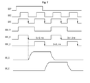
- FIG. 7 shows examples of the first and second gate pulses GO_O and GO_E output by the gate IC.
- the GOE division part 300 includes a 2-frequency divider circuit 301, an inverter 305, and first and second AND operators 311 and 312 implemented by AND gates.
- the 2-frequency divider circuit 301 receives the gate output enable signal GOE to generate a 2-frequency divided gate output enable signal (GOE/2) having 1/2 the frequency of the gate output enable signal GOE.
- the first AND operator 311 receives the 2-frequency divided gate output enable signal GOE/2 and the gate output enable signal GOE to output an AND operation result. That is, the first AND operator 311 outputs a high logic signal only during periods in which both of the 2-frequency divided gate output enable signal GOE/2 and the gate output enable signal GOE have a high logic level.
- the first gate output enable signal GOE_O which is an output signal of the first AND operator 311, controls the output timing of the first gate pulse GO_O output to the odd-numbered gate lines.
- the second AND operator 312 receives an inverted 2-frequency divided gate output enable signal (GOE/2) from the inverter 305 and the gate output enable signal GOE to output an AND operation result, thereby generating the second gate output enable signal GOE_E. That is, the second AND operator 312 outputs a high logic signal only during periods in which both of the inverted 2-frequency divided gate output enable signal GOE/2 and the gate output enable signal GOE have a high logic level.
- the second gate output enable signal GOE_E which is an output signal of the second AND operator 312, controls the output timing of the second gate pulse GO_E output to the even-numbered gate lines.
- each of the gate ICs 331 to 335 may include a GOE division part 300, a shift register 360, a level shifter 370, and third and fourth AND operators 365 and 367 implemented by AND gates.
- the shift register 360 of each of the gate ICs 331 to 335 shifts a gate start pulse GSP at every rising edge of a gate shift clock GSC by using a plurality of sequentially connected flip-flops. Therefore, the shift register 360 of each of the gate ICs 331 to 335 sequentially generates outputs through the output of each of the flip-flops.
- the timing controller 31 supplies the gate start pulse GSP having a high logic level for a period longer than one horizontal period (H) to the gate ICs 331 to 335.
- the gate start pulse GSP may have a high logic level for more than 1 and less than to 2 horizontal periods (H).
- this example embodiment of the present invention can prevent a gate-off phenomenon since the high logic period of the gate start pulse GSP is longer than one horizontal period (H).
- Each of the third AND operators 365 of the gate IC 331 generates an AND output of an output of the shift register 360 and a first gate output enable signal GOE_O inverted by the first inverter 361.
- each of the fourth AND operators 367 generates an AND output of an output of the shift register 360 and a second gate output enable signal GOE_E inverted by the second inverter 362.
- one period of the gate output enable signal GOE is one horizontal period (H)
- one period of the first gate output enable signal GOE_O becomes two horizontal periods (H).
- the first gate output enable signal GOE_O is output as a high logic signal only during periods while both of the gate output enable signal GOE and the 2-frequency divided gate output enable signal GOE/2 have a high logic level. Therefore, the high logic period of the first gate output enable signal GOE_O is determined by the period of the gate output enable signal GOE.
- the first gate output enable signal GOE_O and the second gate output enable signal GOE_E may maintain a high logic level for a period shorter than one horizontal period (H).
- the level shifter 370 receives an output of the shift register 360 when the first and second gate output enable signals GOE_O and GOE_E have a low logic level. Eventually, the low logic periods of the first and second gate output enable signals GOE_O and GOE_E result in the high logic periods of the first and second gate pulses GO_O and GO_E.
- the high logic periods of the first and second gate pulses GO_O and GO_E may be within the range of longer than 1 and shorter than 2 horizontal periods (H).
- the first gate output enable signal GOE_O of the example embodiment of the present invention may have a low logic level for one to two horizontal periods (H). Therefore, the first gate pulse GO_O can maintain a high logic level for longer than one but shorter than two horizontal periods (H). That is, the first gate pulse GO_O does not cause a gate-off phenomenon while scanning the odd-numbered gate lines.
- the second gate pulse GO_E can maintain a high logic level for longer than one but shorter than two horizontal periods (H), and thus not cause a gate-off phenomenon while scanning the even-numbered gate lines.
- the time for charging data of the previous frame can be shortened in comparison with the gate pulse in the related art device having a high logic level for two horizontal periods (H).
- a gate pulse GO having a high logic level for two horizontal periods (H) pre-charges data of the previous frame during 't0' to 't1' and then charges data of the current frame during 't1' to 't2'.
- the data voltage difference between the previous frame and the current frame may be very large in a pattern having a large difference in brightness, for example, when black data and white data are sequentially received as shown in FIG. 8 .
- the voltage level is significantly lowered during the pre-charging period, the voltage may not be charged up to a desired voltage level for depicting white data.
- the pre-charging period is from 't0" to 't1'. That is, the first and second gate pulses GO_O and GO_E can decrease the pre-charging period by ' ⁇ t'. Therefore, even when a pattern having a large difference in brightness from frame to frame is received, the first and second gate pulses are less influenced by the voltage level charged by the data of the previous frame during the pre-charging period. Eventually, the first and second gate pulses GO_O and GO_E according to the example embodiment of the present invention can increase the charged data voltage level by ' ⁇ V as compared with the gate pulse GO used in the related art device.
- each of the gate ICs 331 to 335 may include a buffer unit 380.
- the buffers of the buffer unit 380 amplify the first and second gate pulses GO_O and GO_E received from the level shifter 370, and sequentially supply the amplified first and second gate pulses GO_O and GO_E to respective gate lines G1 to Gk.
- the above example embodiment of the present invention has the GOE division part 300 included in each of the gate ICs 331 to 335.
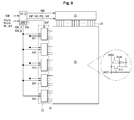
- the GOE division part 300 may be included in the timing controller 31, as shown in FIG. 9 , or may be provided as a separate, standalone circuit, instead of being included in each of the gate ICs 331 to 335.
- the gate pulses having a high logic level for a period longer than one horizontal period (H) may be separately applied to odd-numbered gate lines and even-numbered gate lines, thereby preventing the gate-off phenomenon.
- the charging characteristics of data voltages can be improved by setting the width of the gate pulse to be smaller than two horizontal periods.
Landscapes
- Engineering & Computer Science (AREA)
- Physics & Mathematics (AREA)
- General Physics & Mathematics (AREA)
- Computer Hardware Design (AREA)
- Theoretical Computer Science (AREA)
- Chemical & Material Sciences (AREA)
- Crystallography & Structural Chemistry (AREA)
- Nonlinear Science (AREA)
- Mathematical Physics (AREA)
- Optics & Photonics (AREA)
- Multimedia (AREA)
- Control Of Indicators Other Than Cathode Ray Tubes (AREA)
Abstract
Description
- This application claims the priority benefit of Korean Patent Application No.
10-2013-0168639 - The present invention relates to a display device and a driving method thereof.
- Display devices, which are delivery media of visual information, have been applied to various information devices or office machines. A cathode ray tube or a Braun tube, which is a widely available display device, has a problem that its weight and volume are great. Many kinds of flat panel displays capable of overcoming this limitation of the cathode ray tube have been developed, including a liquid crystal display (LCD), a field emission display (FED), a plasma display panel (PDP), an organic light emitting diode device (OLED), and the like.
- In flat panel displays, data lines and scan lines are arranged orthogonally to each other, and pixels are arranged in a matrix form. In the LCD or OLED, the scan lines are also referred to as gate lines since gate electrodes of TFTs are connected to the scan lines. Video data voltages to be displayed are supplied to the data lines, and scan pulses (or gate pulses) are sequentially supplied to the scan lines. The video data voltages are supplied to pixels of the display lines to which the scan pulses are supplied. While all the display lines are sequentially scanned by scan pulses, video data are displayed.
- Generally, a scan driving circuit for supplying the scan pulses to the scan lines of the flat panel display includes a plurality of scan integrated circuits (hereinafter, referred to as "ICs"). Since each of the scan ICs needs to sequentially output scan pulses, it includes a shift register. It may also include circuits and output buffers for controlling an output voltage of the shift register according to driving characteristics of a display panel. This scan driving circuit operates in response to control signals generated from a timing controller. Hereinafter, a scan driving circuit of a flat panel display will be described based on a scan driving circuit of an LCD.
-
FIG. 1 shows a related art gate IC of a scan driving circuit applied to an LCD. As shown inFIG. 1 , the gate IC includes ashift register 10, alevel shifter 12, and a plurality of logic AND gates 11 (hereinafter, referred to as "AND gates") connected between theshift register 10 and thelevel shifter 12. - The shift register 10 sequentially shifts gate start pulses GSP according to the gate shift clock GSC by using a plurality of dependently connected flip-flops. Each of the
AND gates 11 performs an AND operation on the output signal of the respective flip-flop of theshift register 10 and an inverted gate output enable signal GOE to generate an output. The gate output enable signal GOE is inverted by aninverter 13, and input to one input terminal of theAND gates 11. Thelevel shifter 12 shifts the swing width of the output voltage of theAND gate 11 to an extent at which a TFT of the LCD can operate. Output signals G1 to Gk of theshift register 12 are sequentially supplied to k (k is an integer) gate lines. -
FIG. 2 shows related art examples of control signals for controlling a scan driving circuit and an output signal of the scan driving circuit. As shown inFIG. 2 , a related art gate IC receives a gate start pulse GSP, a gate shift clock GSC, and a gate output enable signal GOE to output gate pulses G1 and G2 of one horizontal period (H), i.e., one cycle of the gate shift clock GSC. - The gate pulses G1 and G2 are for operating TFTs of a flat panel, in this example an LCD panel. In order to supply a voltage that can turn on the TFTs of the LCD panel, the width of a high logic period in the gate pulses G1 and G2 needs to be sufficiently long. In the related art device, as shown in
FIG. 2 , the TFTs can be operated even when the width of the gate pulses G1 and G2 is one horizontal period (H) as a horizontal period (H) tended to be relatively long. However, as the panels become larger and the resolution higher, one horizontal period (H) tends to become shorter. Therefore, when the width of the gate pulses G1 and G2 is set to one horizontal period (H), the TFTs may not be turned on or turned off at a desired timing. - In an effort to solve the above problem, a 'gate overlap' has been proposed in which the width of the high logic period of the gate start pulse GSP is increased to two horizontal periods (H) as show in
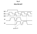
FIG. 3 . - However, when the gate start pulse GSP is input for two horizontal periods (H) as shown in
FIG. 3 , a 'gate off phenomenon may occur in which the voltage level of the gate pulses G1 and G2 falls during the high logic period of the gate output enable signal GOE, thereby potentially causing a temporary cut-off period while source output data are to be transferred to pixels of the panel. - Moreover, when the high logic period of the gate pulses G1 and G2 is maintained for two horizontal periods (H) without the 'gate-off' phenomenon, the voltage charged in the pixels of the LCD panel is influenced by the data voltage of the previous frame during one horizontal period (H) while the gate pulses G1 and G2 overlap each other. Therefore, when the difference in data from the previous frame to the current frame is large, the charge rate of a source output waveform may fall.
- Accordingly, the present invention is directed to a display device and a driving method thereof that substantially obviate one or more of the problems due to limitations and disadvantages of the related art.
- An object of the present invention is to provide a display device capable of preventing the occurrence of a 'gate off phenomenon' and improving the charging characteristics of data voltages, and a driving method thereof.
- Additional features and advantages of the invention will be set forth in the description which follows, and in part will be apparent from the description, or may be learned by practice of the invention. The objectives and other advantages of the invention will be realized and attained by the structure particularly pointed out in the written description and claims hereof as well as the appended drawings.
- To achieve these and other advantages and in accordance with the purpose of the present invention, as embodied and broadly described, a display device includes: a display panel having a plurality of data lines and a plurality of gate lines crossing the data lines, the gate lines including a plurality of odd-numbered gate lines and a plurality of even-numbered gate lines; a timing controller to generate a gate output enable signal; a gate output enable signal division circuit to generate a first gate output enable signal and a second gate output enable signal based on the gate output signal, wherein the first and second gate output enable signals each have a lower frequency than the gate output enable signal; and a gate driver to supply a first gate pulse to at least one of the odd-numbered gate lines based on the first gate output enable signal and a second gate pulse to at least one of the even-numbered gate lines based on the second gate output enable signal. In one or more embodiments, the gate output enable signal division circuit is configured to extract odd-numbered high logic periods of the gate output enable signal to output the first gate output enable signal and to extract even-numbered high logic periods of the gate output enable signal to output the second gate output enable signal; and the gate driver is configured to supply the first gate pulse to the at least one of the odd-numbered gate lines in response to the first gate output enable signal and to supply the second gate pulse to the at least one of the even-numbered gate lines in response to the second output enable signal. In one or more embodiments, the timing controller is also configured to generate a gate shift clock signal, and the first and second gate pulses overlap each other for a period shorter than one cycle of the gate shift clock signal. In one or more embodiments, the timing controller is also configured to generate a gate shift clock signal; and at least one of the first and second gate pulses has a width longer than one cycle of the gate shift clock signal and shorter than two cycles of the gate shift clock signal. In one or more embodiments, the timing controller is also configured to generate a gate start pulse having a width longer than one cycle of the gate shift clock and shorter than two cycles of the gate shift clock signal, and the gate driver is configured to receive the gate start pulse and supply the first and second gate pulses based on the gate start pulse. In one or more embodiments, the first and second gate pulses overlap each other for a period shorter than one cycle of the gate shift clock signal. In one or more embodiments, the gate output enable signal division circuit includes: a 2-frequency divider circuit to divide the frequency of the gate output enable signal by 2 and to generate a 2-frequency divided gate output enable signal; a first inverter to invert the phase of the 2-frequency divided gate output enable signal; a first AND operator to receive the 2-frequency divided gate output enable signal and the gate output enable signal as inputs and to output the first gate output enable signal; and a second AND operator to receive the inverted 2-frequency divided gate output enable signal and the gate output enable signal as inputs and to output the second gate output enable signal. In one or more embodiments, the gate driver includes: a shift register to receive a gate start pulse and the gate shift clock signal from the timing controller, and to output a first output and a second output; a second inverter to invert the phase of the first gate output enable signal and to output the inverted first gate output enable signal; a third inverter to invert the phase of the second gate output enable signal and to output the inverted second gate output enable signal; a third AND operator to receive the first output from the shift register and the inverted first gate output enable signal and to generate a first AND output; a fourth AND operator to receive the second output from the shift register and the inverted second gate output enable signal and to generate a second AND output; and a level shifter to generate the first gate pulse based on the first AND output and the second gate pulse based on the second AND output. In one or more embodiments, the gate driver further includes a buffer unit to amplify the first and second gate pulses, and to supply the amplified first gate pulse to the at least one of the odd-numbered gate lines and the amplified second gate pulse to the at least one of the even-numbered gate lines. In one or more embodiments, the gate output enable signal division circuit is included in the gate driver. In one or more embodiments, the gate output enable signal division circuit is included in the timing controller.
- In another aspect of the present invention, a display device includes: a display panel having a plurality of data lines and a plurality of gate lines crossing the data lines, the gate lines including a plurality of odd-numbered gate lines and a plurality of even-numbered gate lines; a timing controller to generate a gate output enable signal; a gate output enable signal division circuit to extract odd-numbered high logic periods of the gate output enable signal to output a first gate output enable signal and to extract even-numbered high logic periods of the gate output enable signal to output a second gate output enable signal; and a gate driver to supply a first gate pulse to at least one of the odd-numbered gate lines in response to the first gate output enable signal and a second gate pulse to at least one of the even-numbered gate lines in response to the second output enable signal. In one or more embodiments, the timing controller is also configured to generate a gate shift clock signal, and at least one of the first and second gate pulses has a width that is longer than one cycle of the gate shift clock signal but shorter than two cycles of the gate shift clock signal. In one or more embodiments, the timing controller is also configured to generate a gate shift clock signal, and the first and second gate pulses overlap each other for a period shorter than one cycle of the gate shift clock signal. In one or more embodiments, the gate output enable signal division circuit includes: a 2-frequency divider circuit to divide the frequency of the gate output enable signal by 2 and to output a 2-frequency divided gate output enable signal; a first inverter to invert the phase of the 2-frequency divided gate output enable signal; a first AND operator to receive the 2-frequency divided gate output enable signal and the gate output enable signal as inputs and to output the first gate output enable signal; and a second AND operator to receive the inverted 2-frequency divided gate output enable signal and the gate output enable signal as inputs and to output the second gate output enable signal. In one or more embodiments, the gate driver includes: a shift register to receive a gate start pulse and a gate shift clock signal from the timing controller, and to output a first output and a second output; a second inverter to invert the phase of the first gate output enable signal and to output the inverted first gate output enable signal; a third inverter to invert the phase of the second gate output enable signal and to output the inverted second gate output enable signal; a third AND operator to receive the first output from the shift register and the inverted first gate output enable signal and to generate a first AND output; a fourth AND gate to receive the second output from the shift register and the inverted second gate output enable signal and to generate a second AND output; and a level shifter to generate the first gate pulse based on the first AND output and the second gate pulse based on the second AND output. In one or more embodiments, the gate driver further includes a buffer unit to amplify the first and second gate pulses, and to supply the amplified first gate pulse to the at least one of the odd-numbered gate lines and the amplified second gate pulse to the at least one of the even-numbered gate lines. In one or more embodiments, the gate output enable signal division circuit is included in the gate driver. In one or more embodiments, the gate output enable signal division circuit is included in the timing controller.
- In another aspect of the present invention, a display device includes: a display panel having a plurality of data lines and a plurality of gate lines crossing the data lines, the gate lines including a plurality of odd-numbered gate lines and a plurality of even-numbered gate lines; a timing controller to generate a gate output enable signal and a gate shift clock signal; a gate output enable signal division circuit to generate a first gate output enable signal and a second gate output enable signal based on the gate output enable signal; and a gate IC to supply a first gate pulse to at least one of the odd-numbered gate lines based on the first gate output enable signal and a second gate pulse to at least one of the even-numbered gate lines based on the second output enable signal, wherein at least one of the first and second gate pulses has a width longer than one cycle of the gate shift clock signal and shorter than two cycles of the gate shift clock signal. In one or more embodiments, the timing controller is also configured to generate a gate start pulse having a width longer than one cycle of the gate shift clock and shorter than two cycles of the gate shift clock signal, and the gate IC is configured to receive the gate start pulse and supply the first and second gate pulses based on the gate start pulse. In one or more embodiments, the gate output enable signal division circuit includes: a 2-frequency divider circuit to divide the frequency of the gate output enable signal by 2 and to generate a 2-frequency divided gate output enable signal; a first inverter to invert the phase of the 2-frequency divided gate output enable signal; a first AND operator to receive the 2-frequency divided gate output enable signal and the gate output enable signal as inputs and to output the first gate output enable signal; and a second AND operator to receive the inverted 2-frequency divided gate output enable signal and the gate output enable signal as inputs and to output the second gate output enable signal. In one or more embodiments, the first and second gate pulses overlap each other for a period shorter than one cycle of the gate shift clock signal. In one or more embodiments, the gate IC includes: a shift register to receive a gate start pulse and the gate shift clock signal from the timing controller, and to output a first output and a second output; a second inverter to invert the phase of the first gate output enable signal and to output the inverted first gate output enable signal; a third inverter to invert the phase of the second gate output enable signal and to output the inverted second gate output enable signal; a third AND operator to receive the first output from the shift register and the inverted first gate output enable signal and to generate a first AND output; a fourth AND gate to receive the second output from the shift register and the inverted second gate output enable signal and to generate a second AND output; and a level shifter to generate the first gate pulse based on the first AND output and the second gate pulse based on the second AND output. In one or more embodiments, the gate IC further includes a buffer unit to amplify the first and second gate pulses, and to supply the amplified first gate pulse to the at least one of the odd-numbered gate lines and the amplified second gate pulse to the at least one of the even-numbered gate lines. In one or more embodiments, the gate output enable signal division circuit is included in the gate IC. In one or more embodiments, the gate output enable signal division circuit is included in the timing controller.
- In yet another aspect of the present invention, it is provided a method for driving a display device with a display panel having a plurality of data lines and a plurality of gate lines crossing the data lines, the gate lines including a plurality of odd-numbered gate lines and a plurality of even-numbered gate lines is disclosed, the method including: receiving a gate output enable signal; generating a first gate output enable signal and a second gate output enable signal based on the gate output enable signal, wherein the first and second gate output enable signals each have a lower frequency than the gate output enable signal; supplying a first gate pulse to at least one of the odd-numbered gate lines based on the first gate output enable signal; and supplying a second gate pulse to at least one of the even-numbered gate lines based on the second gate output enable signal. In one or more embodiments, the method further comprises receiving a gate start pulse and a gate shift clock signal, wherein the gate start pulse has a width longer than one cycle of the gate shift clock signal and shorter than two cycles of the gate shift clock signal. In one or more embodiments, the method further comprises receiving a gate shift clock signal, wherein at least one of the first and second gate pulses has a width longer than one cycle of the gate shift clock and shorter than two cycles of the gate shift clock signal. In one or more embodiments, the method further comprises receiving a gate shift clock signal, wherein the first and second gate pulses overlap each other for a period shorter than one cycle of the gate shift clock signal. In one or more embodiments, the generating of the first and second gate output enable signals includes: extracting odd-numbered high logic periods of the gate output enable signal to generate the first gate output enable signal; and extracting even-numbered high logic periods of the gate output enable signal to generate the second gate output enable signal. In one or more embodiments, the generating of the first and second gate output enable signals includes: dividing the frequency of the gate output enable signal by 2 to generate a 2-frequency divided gate output enable signal; inverting the 2-frequency divided gate output enable signal to generate an inverted 2-frequency divided gate output enable signal: performing an AND operation on the 2-frequency divided gate output enable signal and the gate output enable signal to generate the first gate output enable signal; and performing an AND operation on the inverted 2-frequency divided gate output enable signal and the gate output enable signal to generate the second gate output enable signal.
- It is to be understood that both the foregoing general description and the following detailed description are exemplary and explanatory and are intended to provide further explanation of the invention as claimed.
- The accompanying drawings, which are included to provide a further understanding of the invention and are incorporated in and constitute a part of this specification, illustrate embodiments of the invention and together with the description serve to explain the principles of the invention. In the drawings:
-
FIG. 1 is a circuit diagram showing an example of a gate IC according to the related art; -
FIGs. 2 and3 are waveform diagrams showing gate control signals and gate pulses according to the related art; -
FIG. 4 is a diagram showing a liquid crystal display according to the first example embodiment of the present invention; -
FIG. 5 is a circuit diagram showing a gate output enable signal division part according to an example embodiment of the present invention; -
FIG. 6 is a circuit diagram showing an example of a gate IC according to an example embodiment of the present invention; -
FIG. 7 is a waveform diagram showing first and second gate output enable signals and first and second gate pulses according to an example embodiment of the present invention; -
FIG. 8 is a view illustrating charging characteristics of gate pulses according to an example embodiment of the present invention; and -
FIG. 9 is a diagram showing a liquid crystal display according to the second example embodiment of the present invention. - Reference will now be made in detail to the embodiments of the present invention, examples of which are illustrated in the accompanying drawings. Wherever possible, the same reference numbers will be used throughout the drawings to refer to the same or like parts.
- The present invention may be similarly applied to a number of different display devices, such as a liquid crystal display (LCD), a field emission display (FED), a plasma display panel (PDP), and organic light emitting diode device (OLED). The below detailed description is based on an example embodiment of the liquid crystal display.
-
FIG. 4 is a diagram showing a liquid crystal display according to an example embodiment of the present invention. - As shown in
FIG. 4 , the liquid crystal display according to an example embodiment of the present invention includes a liquidcrystal display panel 30, atiming controller 31, adata driving circuit 32, and ascan driving circuit 33. Thedata driving circuit 32 may include one or more source ICs. Thescan driving circuit 33 may include one ormore gate ICs 331 to 335. AlthoughFIG. 4 illustrates an example where gate ICs are on one side of the display, the display may include gate ICs on both sides of the display. As yet another alternative example, the display may include gate drivers on one or both sides of a display panel substrate without the use of gate ICs. - In the liquid
crystal display panel 30, a liquid crystal layer is formed between two substrates. The liquidcrystal display panel 30 includes m x n liquid crystal cells Clc arranged in a matrix format at or near the crossings of m data lines 34 and n gate lines 35, where 'm' and 'n' are integers. - The data lines 34, the gate lines 35, TFTs, and storage capacitors Cst are formed on a lower substrate of the liquid
crystal display panel 30. The liquid crystal cells Clc are connected to the TFTs, and are driven by an electric field between pixel electrodes 1 and acommon electrode 2. A black matrix (not shown) and color filters (not shown) may be formed on an upper substrate of the liquidcrystal display panel 30. Alternatively, color filters (not shown) may be formed on an upper substrate without a separate black matrix. Thecommon electrode 2 may be formed on the upper substrate in a device employing a vertical electric field driving mode, such as twisted nematic (TN) mode and a vertical alignment (VA) mode. Alternatively, thecommon electrode 2 may be formed along with the pixel electrode 1 on the lower substrate in a device employing a horizontal electric field driving mode, such as an in-plane field switching (IPS) mode or a fringe field switching (FFS) mode. A polarizer (not shown) may be attached to each of the upper substrate and the lower substrate of theliquid crystal panel 30. An alignment film (not shown) for setting a pre-tilt angle of liquid crystals may also be formed on one or both of the substrates at an interface in contact with the liquid crystals. - The
timing controller 31 may receive timing signals, such as vertical and horizontal synchronization signals Vsync and Hsync, a data enable signal DE, and a clock signal CLK to generate control signals for controlling operation timings of thedata driving circuit 32 and thescan driving circuit 33. These control signals may include a gate timing control signal and a data timing control signal. In addition, thetiming controller 31 may supply digital video data (RGB) to thedata driving circuit 32. - The gate timing control signal generated by the
timing controller 31 may include a gate start pulse GSP, a gate shift clock signal GSC, and a gate output enable signal GOE. - The gate start pulse GSP is applied to the
first gate IC 331 to indicate a start line from which the scanning starts so that a first gate pulse is generated from thefirst gate IC 331. - The gate shift clock signal GSC is a clock signal for shifting the gate start pulse GSP. Shift registers of the
gate ICs 331 to 335 shift the gate start pulse GSP at a rising edge of the gate shift clock signal GSC. Each of the second tofifth gate ICs 332 to 335 receives a carry signal from the previous gate IC as a gate start pulse GSP to generate a first gate pulse. Although this example embodiment uses five gate ICs, a different number of gate ICs may be employed. - The gate output enable signal GOE is commonly input to the
gate ICs 331 to 335. Thegate ICs 331 to 335 output the gate pulses during a low logic period of the gate output enable signal GOE, i.e., during a period between the falling edge of the previous pulse and the rising edge of the next pulse. During a high logic period of the gate output enable signal GOE, the outputs of thegate ICs 331 to 335 are cut off. - The data timing control signals generated by the
timing controller 31 may include such signals as a source start pulse SSP, a source sampling clock SSC, a polarity control signal POL, and a source output enable signal SOE. The source start pulse SSP indicates a start pixel in a line on which data are to be displayed. The source sampling clock SSC indicates a latching operation of data in thedata driving circuit 32 based on a rising or falling edge. The polarity control signal POL controls the polarity of an analog video data voltage output from thedata driving circuit 32. The source output enable signal SOE controls outputs of the source ICs. - Each of the source ICs of the
data driving circuit 32 may include a shift register (not shown), a latch circuit (not shown), a digital-to-analog converter (not shown), and an output buffer (not shown). Thedata driving circuit 32 latches digital video data RGB under the control of thetiming controller 31. In addition, the source ICs of thedata driving circuit 32 supply charge share voltages to the data lines 34 in response to the source output enable signal SOE, convert the digital video data RGB into a positive or negative analog gamma compensation voltages in response to the polarity control signal POL to generate positive or negative analog data voltages, and then supply the data voltages to the data lines 34. - Each of the
gate ICs 331 to 335 according to an example embodiment of the present invention outputs first and second gate pulses GO_O and GO_E for driving odd-numbered gate lines and even-numbered gate lines, respectively. Each of thegate ICs 331 to 335 includes a gate output enable division part (hereinafter, GOE division part) 300 for dividing the gate output enable signal GOE received from thetiming controller 31 into first and second gate output enable signals GOE_O and GOE_E. TheGOE division part 300 outputs the odd-numbered high logic periods of the gate output enable signal GOE as a first gate output enable signal GOE_O, and outputs even-numbered high logic periods of the gate output enable signal GOE as a second gate output enable signal GOE_E. -
FIG. 5 shows an example of theGOE division part 300 for outputting the first and second gate output enable signals according to an example embodiment of the present invention.FIG. 6 shows an example gate IC including the exampleGOE division part 300 shown inFIG. 5 , andFIG. 7 shows examples of the first and second gate pulses GO_O and GO_E output by the gate IC. - As shown in
FIGs. 5 to 7 , theGOE division part 300 includes a 2-frequency divider circuit 301, aninverter 305, and first and second ANDoperators - The 2-
frequency divider circuit 301 receives the gate output enable signal GOE to generate a 2-frequency divided gate output enable signal (GOE/2) having 1/2 the frequency of the gate output enable signal GOE. - The first AND
operator 311 receives the 2-frequency divided gate output enable signal GOE/2 and the gate output enable signal GOE to output an AND operation result. That is, the first ANDoperator 311 outputs a high logic signal only during periods in which both of the 2-frequency divided gate output enable signal GOE/2 and the gate output enable signal GOE have a high logic level. The first gate output enable signal GOE_O, which is an output signal of the first ANDoperator 311, controls the output timing of the first gate pulse GO_O output to the odd-numbered gate lines. - The second AND
operator 312 receives an inverted 2-frequency divided gate output enable signal (GOE/2) from theinverter 305 and the gate output enable signal GOE to output an AND operation result, thereby generating the second gate output enable signal GOE_E. That is, the second ANDoperator 312 outputs a high logic signal only during periods in which both of the inverted 2-frequency divided gate output enable signal GOE/2 and the gate output enable signal GOE have a high logic level. The second gate output enable signal GOE_E, which is an output signal of the second ANDoperator 312, controls the output timing of the second gate pulse GO_E output to the even-numbered gate lines. - As shown in
FIGs. 5 to 7 , each of thegate ICs 331 to 335 may include aGOE division part 300, ashift register 360, alevel shifter 370, and third and fourth ANDoperators - The
shift register 360 of each of thegate ICs 331 to 335 shifts a gate start pulse GSP at every rising edge of a gate shift clock GSC by using a plurality of sequentially connected flip-flops. Therefore, theshift register 360 of each of thegate ICs 331 to 335 sequentially generates outputs through the output of each of the flip-flops. - Here, the
timing controller 31 supplies the gate start pulse GSP having a high logic level for a period longer than one horizontal period (H) to thegate ICs 331 to 335. For example, the gate start pulse GSP may have a high logic level for more than 1 and less than to 2 horizontal periods (H). As such, this example embodiment of the present invention can prevent a gate-off phenomenon since the high logic period of the gate start pulse GSP is longer than one horizontal period (H). - Each of the third AND
operators 365 of thegate IC 331 generates an AND output of an output of theshift register 360 and a first gate output enable signal GOE_O inverted by thefirst inverter 361. In addition, each of the fourth ANDoperators 367 generates an AND output of an output of theshift register 360 and a second gate output enable signal GOE_E inverted by thesecond inverter 362. - When one period of the gate output enable signal GOE is one horizontal period (H), one period of the first gate output enable signal GOE_O becomes two horizontal periods (H). In addition, the first gate output enable signal GOE_O is output as a high logic signal only during periods while both of the gate output enable signal GOE and the 2-frequency divided gate output enable signal GOE/2 have a high logic level. Therefore, the high logic period of the first gate output enable signal GOE_O is determined by the period of the gate output enable signal GOE. For example, the first gate output enable signal GOE_O and the second gate output enable signal GOE_E may maintain a high logic level for a period shorter than one horizontal period (H).
- The
level shifter 370 receives an output of theshift register 360 when the first and second gate output enable signals GOE_O and GOE_E have a low logic level. Eventually, the low logic periods of the first and second gate output enable signals GOE_O and GOE_E result in the high logic periods of the first and second gate pulses GO_O and GO_E. For example, the high logic periods of the first and second gate pulses GO_O and GO_E may be within the range of longer than 1 and shorter than 2 horizontal periods (H). - Accordingly, the first gate output enable signal GOE_O of the example embodiment of the present invention may have a low logic level for one to two horizontal periods (H). Therefore, the first gate pulse GO_O can maintain a high logic level for longer than one but shorter than two horizontal periods (H). That is, the first gate pulse GO_O does not cause a gate-off phenomenon while scanning the odd-numbered gate lines.
- Similarly, the second gate pulse GO_E can maintain a high logic level for longer than one but shorter than two horizontal periods (H), and thus not cause a gate-off phenomenon while scanning the even-numbered gate lines.
- In addition, since the first gate pulse GO_O or the second gate pulse GO_E according to the example embodiment of the present invention has a high logic level for a period shorter than two horizontal periods (H), the time for charging data of the previous frame can be shortened in comparison with the gate pulse in the related art device having a high logic level for two horizontal periods (H).
- This will be described with reference to
FIG. 8 as follows. In the related art device, a gate pulse GO having a high logic level for two horizontal periods (H) pre-charges data of the previous frame during 't0' to 't1' and then charges data of the current frame during 't1' to 't2'. The data voltage difference between the previous frame and the current frame may be very large in a pattern having a large difference in brightness, for example, when black data and white data are sequentially received as shown inFIG. 8 . When there is such a large difference in data voltages, because the voltage level is significantly lowered during the pre-charging period, the voltage may not be charged up to a desired voltage level for depicting white data. - In contrast, according to the example embodiment of the present invention, since the first and second gate pulses GO_O and GO_E maintain a high logic level during a period shorter than two horizontal periods (H), the pre-charging period is from 't0" to 't1'. That is, the first and second gate pulses GO_O and GO_E can decrease the pre-charging period by 'Δt'. Therefore, even when a pattern having a large difference in brightness from frame to frame is received, the first and second gate pulses are less influenced by the voltage level charged by the data of the previous frame during the pre-charging period. Eventually, the first and second gate pulses GO_O and GO_E according to the example embodiment of the present invention can increase the charged data voltage level by 'ΔV as compared with the gate pulse GO used in the related art device.
- In addition, each of the
gate ICs 331 to 335 may include abuffer unit 380. The buffers of thebuffer unit 380 amplify the first and second gate pulses GO_O and GO_E received from thelevel shifter 370, and sequentially supply the amplified first and second gate pulses GO_O and GO_E to respective gate lines G1 to Gk. - The above example embodiment of the present invention has the
GOE division part 300 included in each of thegate ICs 331 to 335. Alternatively, however, theGOE division part 300 may be included in thetiming controller 31, as shown inFIG. 9 , or may be provided as a separate, standalone circuit, instead of being included in each of thegate ICs 331 to 335. - According to the present invention, the gate pulses having a high logic level for a period longer than one horizontal period (H) may be separately applied to odd-numbered gate lines and even-numbered gate lines, thereby preventing the gate-off phenomenon.
- Further, according to the present invention, the charging characteristics of data voltages can be improved by setting the width of the gate pulse to be smaller than two horizontal periods.
- It will be apparent to those skilled in the art that various modifications and variations can be made in the display device and driving method of the present invention without departing from the spirit or scope of the invention. Thus, it is intended that the present invention cover the modifications and variations of this invention provided they come within the scope of the appended claims and their equivalents.
Claims (17)
- A display device, comprising:a display panel (30) having a plurality of data lines (34) and a plurality of gate lines (35) crossing the data lines, the gate lines including a plurality of odd-numbered gate lines and a plurality of even-numbered gate lines;a timing controller (31) to generate a gate output enable signal (GOE);a gate output enable signal division circuit (300) to generate a first gate output enable signal (GOE_O) and a second gate output enable signal (GOE_E) based on the gate output signal (GOE), wherein the first and second gate output enable signals (GOE_O, GOE_E) each have a lower frequency than the gate output enable signal (GOE); anda gate driver (331-335) to supply a first gate pulse (GO_O) to at least one of the odd-numbered gate lines based on the first gate output enable signal (GOE_O) and a second gate pulse (GO_E) to at least one of the even-numbered gate lines based on the second gate output enable signal (GOE_E).
- The display device of claim 1,
wherein the gate output enable signal division circuit (300) is configured to extract odd-numbered high logic periods of the gate output enable signal (GOE) to output the first gate output enable signal (GOE_O) and to extract even-numbered high logic periods of the gate output enable signal (GOE) to output the second gate output enable signal (GOE_E); and
wherein the gate driver (331-335) is configured to supply the first gate pulse (GO_O) to the at least one of the odd-numbered gate lines in response to the first gate output enable signal (GOE_O) and to supply the second gate pulse (GO_E) to the at least one of the even-numbered gate lines in response to the second output enable signal (GOE_E). - The display device of claim 2, wherein the timing controller (31) is also configured to generate a gate shift clock signal (GSC), and
wherein the first and second gate pulses (GO_O, GO_E) overlap each other for a period shorter than one cycle of the gate shift clock signal (GSC). - The display device of claim 1,
wherein the timing controller (31) is also configured to generate a gate shift clock signal (GSC); and
wherein at least one of the first and second gate pulses (GO_O, GO_E) has a width longer than one cycle of the gate shift clock signal (GSC) and shorter than two cycles of the gate shift clock signal (GSC). - The display device of claim 4, wherein the timing controller (31) is also configured to generate a gate start pulse (GSP) having a width longer than one cycle of the gate shift clock (GSC) and shorter than two cycles of the gate shift clock signal (GSC), and
wherein the gate driver (31) is configured to receive the gate start pulse (GSP) and supply the first and second gate pulses (GO_O, GO_E) based on the gate start pulse. - The display device of claim 5, wherein the first and second gate pulses (GO_O, GO_E) overlap each other for a period shorter than one cycle of the gate shift clock signal (GSC).
- The display device of any one of claims 1 to 6, wherein the gate output enable signal division circuit (300) includes:a 2-frequency divider circuit (301) to divide the frequency of the gate output enable signal (GOE) by 2 and to generate a 2-frequency divided gate output enable signal (GOE/2);a first inverter (305) to invert the phase of the 2-frequency divided gate output enable signal (GOE/2);a first AND operator (311) to receive the 2-frequency divided gate output enable signal (GOE/2) and the gate output enable signal (GOE) as inputs and to output the first gate output enable signal (GOE_O); anda second AND operator (312) to receive the inverted 2-frequency divided gate output enable signal (GOE/2) and the gate output enable signal (GOE) as inputs and to output the second gate output enable signal (GOE_E).
- The display device of any one of claims 1 to 7, wherein the gate driver (331-335) includes:a shift register (360) to receive a gate start pulse (GSP) and the gate shift clock signal (GSC) from the timing controller (31), and to output a first output and a second output;a second inverter (361) to invert the phase of the first gate output enable signal (GOE_O) and to output the inverted first gate output enable signal;a third inverter (362) to invert the phase of the second gate output enable signal (GOE_E) and to output the inverted second gate output enable signal;a third AND operator (365) to receive the first output from the shift register (360) and the inverted first gate output enable signal and to generate a first AND output;a fourth AND operator (367) to receive the second output from the shift register (360) and the inverted second gate output enable signal and to generate a second AND output; anda level shifter (370) to generate the first gate pulse (GO_O) based on the first AND output and the second gate pulse (GO_E) based on the second AND output.
- The display device of claim 8, wherein the gate driver (331-335) further includes a buffer unit (380) to amplify the first and second gate pulses (GO_O, GO_E), and to supply the amplified first gate pulse to the at least one of the odd-numbered gate lines and the amplified second gate pulse to the at least one of the even-numbered gate lines.
- The display device of any one of claims 1 to 9, wherein the gate output enable signal division circuit (300) is included in the gate driver (331-335).
- The display device of any one of claims 1 to 10, wherein the gate output enable signal division circuit (300) is included in the timing controller (31).
- A method for driving a display device with a display panel (30) having a plurality of data lines (34) and a plurality of gate lines (35) crossing the data lines, the gate lines including a plurality of odd-numbered gate lines and a plurality of even-numbered gate lines, the method comprising:receiving a gate output enable signal (GOE);generating a first gate output enable signal (GOE_O) and a second gate output enable signal (GOE_E) based on the gate output enable signal (GOE), wherein the first and second gate output enable signals (GOE_O, GOE_E) each have a lower frequency than the gate output enable signal (GOE);supplying a first gate pulse (GO_O) to at least one of the odd-numbered gate lines based on the first gate output enable signal (GOE_O); andsupplying a second gate pulse (GO_E) to at least one of the even-numbered gate lines based on the second gate output enable signal (GOE_E).
- The method of claim 12, further comprising receiving a gate start pulse (GSP) and a gate shift clock signal (GSC),
wherein the gate start pulse (GSP) has a width longer than one cycle of the gate shift clock signal (GSC) and shorter than two cycles of the gate shift clock signal (GSC). - The method of claim 12, further comprising receiving a gate shift clock signal (GSC),
wherein at least one of the first and second gate pulses (GO_O, GO_E) has a width longer than one cycle of the gate shift clock (GSC) and shorter than two cycles of the gate shift clock signal (GSC). - The method of claim 12, further comprising receiving a gate shift clock signal (GSC),
wherein the first and second gate pulses (GO_O, GO_E) overlap each other for a period shorter than one cycle of the gate shift clock signal (GSC). - The method of any one of claims 12 to 15, wherein the generating of the first and second gate output enable signals (GOE_O, GO_E) includes:extracting odd-numbered high logic periods of the gate output enable signal (GOE) to generate the first gate output enable signal (GOE_O); andextracting even-numbered high logic periods of the gate output enable signal (GOE) to generate the second gate output enable signal (GOE_E).
- The method of any one of claims 12 to 16, wherein the generating of the first and second gate output enable signals (GOE_O, GOE_E) includes:dividing the frequency of the gate output enable signal by 2 to generate a 2-frequency divided gate output enable signal (GOE/2);inverting the 2-frequency divided gate output enable signal (GOE/2) to generate an inverted 2-frequency divided gate output enable signal;performing an AND operation on the 2-frequency divided gate output enable signal (GOE/2) and the gate output enable signal (GOE) to generate the first gate output enable signal (GOE_O); andperforming an AND operation on the inverted 2-frequency divided gate output enable signal and the gate output enable signal to generate the second gate output enable signal (GOE_E).
Applications Claiming Priority (1)
| Application Number | Priority Date | Filing Date | Title |
|---|---|---|---|
| KR1020130168639A KR102147375B1 (en) | 2013-12-31 | 2013-12-31 | Liquid Crystal Display and Driving Method thereof |
Publications (2)
| Publication Number | Publication Date |
|---|---|
| EP2889872A1 true EP2889872A1 (en) | 2015-07-01 |
| EP2889872B1 EP2889872B1 (en) | 2019-08-21 |
Family
ID=52144530
Family Applications (1)
| Application Number | Title | Priority Date | Filing Date |
|---|---|---|---|
| EP14199724.7A Active EP2889872B1 (en) | 2013-12-31 | 2014-12-22 | Display device and driving method thereof |
Country Status (4)
| Country | Link |
|---|---|
| US (1) | US9224349B2 (en) |
| EP (1) | EP2889872B1 (en) |
| KR (1) | KR102147375B1 (en) |
| CN (1) | CN104751812B (en) |
Families Citing this family (9)
| Publication number | Priority date | Publication date | Assignee | Title |
|---|---|---|---|---|
| CN104810001B (en) * | 2015-05-14 | 2017-11-10 | 深圳市华星光电技术有限公司 | The drive circuit and driving method of a kind of liquid crystal display panel |
| KR102364744B1 (en) * | 2015-08-20 | 2022-02-21 | 삼성디스플레이 주식회사 | Gate driver, display apparatus having the gate driver and method of driving the display apparatus |
| TWI590214B (en) * | 2016-05-20 | 2017-07-01 | 友達光電股份有限公司 | Displaying device |
| CN109377957B (en) * | 2018-12-03 | 2020-05-05 | 惠科股份有限公司 | Driving method, driving circuit and display device |
| CN109935220B (en) * | 2019-04-17 | 2022-01-25 | Tcl华星光电技术有限公司 | Drive circuit and display device |
| KR102688476B1 (en) * | 2019-11-04 | 2024-07-26 | 삼성디스플레이 주식회사 | Display device |
| CN114464119B (en) * | 2020-11-10 | 2024-01-16 | 北京京东方显示技术有限公司 | Chip-on-chip film, display substrate, display device and driving method thereof |
| TWI818338B (en) * | 2021-10-25 | 2023-10-11 | 大陸商常州欣盛半導體技術股份有限公司 | Display device and gate enable method thereof |
| CN117597722A (en) | 2022-03-30 | 2024-02-23 | 京东方科技集团股份有限公司 | Driving circuit, display device and driving method |
Citations (5)
| Publication number | Priority date | Publication date | Assignee | Title |
|---|---|---|---|---|
| US6670944B1 (en) * | 1998-11-26 | 2003-12-30 | Seiko Epson Corporation | Shift register circuit, driving circuit for an electrooptical device, electrooptical device, and electronic apparatus |
| US20090009497A1 (en) * | 2007-07-06 | 2009-01-08 | Samsung Electronics Co., Ltd. | Liquid crystal display and method of driving the same |
| US20120075279A1 (en) * | 2009-06-01 | 2012-03-29 | Tatsuya Ishida | Level shifter circuit, scanning line driver and display device |
| KR20120032338A (en) * | 2010-09-28 | 2012-04-05 | 엘지디스플레이 주식회사 | Stereoscopic image display |
| US20120162054A1 (en) * | 2010-12-23 | 2012-06-28 | Beijing Boe Optoelectronics Technology Co., Ltd. | Gate driver, driving circuit, and lcd |
Family Cites Families (14)
| Publication number | Priority date | Publication date | Assignee | Title |
|---|---|---|---|---|
| JP2006058638A (en) * | 2004-08-20 | 2006-03-02 | Toshiba Matsushita Display Technology Co Ltd | Gate line driving circuit |
| KR101127854B1 (en) * | 2005-09-27 | 2012-03-21 | 엘지디스플레이 주식회사 | Apparatus driving for gate and image display using the same |
| KR101211219B1 (en) * | 2005-10-31 | 2012-12-11 | 엘지디스플레이 주식회사 | Liquid crystal display and driving method thereof |
| KR20070109296A (en) * | 2006-05-10 | 2007-11-15 | 엘지.필립스 엘시디 주식회사 | LCD and its driving method |
| WO2007142190A1 (en) * | 2006-06-09 | 2007-12-13 | Sharp Kabushiki Kaisha | Display drive circuit and display |
| JP5348884B2 (en) * | 2007-01-15 | 2013-11-20 | エルジー ディスプレイ カンパニー リミテッド | Liquid crystal display |
| KR101301769B1 (en) * | 2007-12-21 | 2013-09-02 | 엘지디스플레이 주식회사 | Liquid Crystal Display and Driving Method thereof |
| KR101298438B1 (en) * | 2008-02-27 | 2013-08-20 | 엘지디스플레이 주식회사 | Liquid Crystal Display and Driving Method thereof |
| TWI385633B (en) * | 2008-03-06 | 2013-02-11 | Novatek Microelectronics Corp | Driving device and related transformation device of output enable signals in an lcd device |
| KR101301422B1 (en) * | 2008-04-30 | 2013-08-28 | 엘지디스플레이 주식회사 | Liquid Crystal Display and Driving Method thereof |
| KR101303494B1 (en) * | 2008-04-30 | 2013-09-03 | 엘지디스플레이 주식회사 | Liquid Crystal Display and Driving Method thereof |
| KR101324428B1 (en) * | 2009-12-24 | 2013-10-31 | 엘지디스플레이 주식회사 | Display device |
| US20110164076A1 (en) * | 2010-01-06 | 2011-07-07 | Sang Tae Lee | Cost-effective display methods and apparatuses |
| KR101887680B1 (en) * | 2012-04-26 | 2018-08-13 | 엘지디스플레이 주식회사 | Liquid crystal display |
-
2013
- 2013-12-31 KR KR1020130168639A patent/KR102147375B1/en active Active
-
2014
- 2014-12-15 US US14/569,938 patent/US9224349B2/en active Active
- 2014-12-19 CN CN201410804220.XA patent/CN104751812B/en active Active
- 2014-12-22 EP EP14199724.7A patent/EP2889872B1/en active Active
Patent Citations (5)
| Publication number | Priority date | Publication date | Assignee | Title |
|---|---|---|---|---|
| US6670944B1 (en) * | 1998-11-26 | 2003-12-30 | Seiko Epson Corporation | Shift register circuit, driving circuit for an electrooptical device, electrooptical device, and electronic apparatus |
| US20090009497A1 (en) * | 2007-07-06 | 2009-01-08 | Samsung Electronics Co., Ltd. | Liquid crystal display and method of driving the same |
| US20120075279A1 (en) * | 2009-06-01 | 2012-03-29 | Tatsuya Ishida | Level shifter circuit, scanning line driver and display device |
| KR20120032338A (en) * | 2010-09-28 | 2012-04-05 | 엘지디스플레이 주식회사 | Stereoscopic image display |
| US20120162054A1 (en) * | 2010-12-23 | 2012-06-28 | Beijing Boe Optoelectronics Technology Co., Ltd. | Gate driver, driving circuit, and lcd |
Also Published As
| Publication number | Publication date |
|---|---|
| US20150187297A1 (en) | 2015-07-02 |
| CN104751812A (en) | 2015-07-01 |
| KR102147375B1 (en) | 2020-08-24 |
| CN104751812B (en) | 2017-08-01 |
| KR20150078855A (en) | 2015-07-08 |
| EP2889872B1 (en) | 2019-08-21 |
| US9224349B2 (en) | 2015-12-29 |
Similar Documents
| Publication | Publication Date | Title |
|---|---|---|
| US9224349B2 (en) | Display device and driving method thereof | |
| US9390666B2 (en) | Display device capable of driving at low speed | |
| US9548031B2 (en) | Display device capable of driving at low speed | |
| US8242990B2 (en) | Liquid crystal display having function of suppressing stain and method of driving the same | |
| US8456406B2 (en) | Liquid crystal display and driving method with black voltage charging | |
| US20140320465A1 (en) | Display Device For Low Speed Drive And Method For Driving The Same | |
| KR101236518B1 (en) | Liquid crystal display device and driving method thereof | |
| US8791892B2 (en) | Liquid crystal display capable of rendering video data in accordance with a rendering structure of a double rate driving panel | |
| KR20090114693A (en) | LCD and its driving method | |
| CN101676984A (en) | Liquid crystal display device and memory controlling method thereof | |
| KR101510879B1 (en) | Display device | |
| KR102008133B1 (en) | Display device and driving method thereof | |
| KR20150030533A (en) | Display device and method for driving the same | |
| KR101470627B1 (en) | Display device and driving method thereof | |
| KR100922790B1 (en) | Gate driver of liquid crystal panel | |
| KR101958654B1 (en) | Dot inversion type liquid crystal display device | |
| KR102148489B1 (en) | Power supplying apparatus for display device | |
| KR20080050313A (en) | LCD and its driving method | |
| KR20150078828A (en) | Power supplying apparatus for liquid crystal display | |
| KR20150030831A (en) | Liquid crystal display device | |
| KR102283377B1 (en) | Display device and gate driving circuit thereof | |
| KR102033098B1 (en) | Liquid crystal display device and driving method thereof | |
| KR20130074570A (en) | Shift register and display device including the same | |
| KR101902561B1 (en) | Liquid Crystal Display Device | |
| KR102274434B1 (en) | Display device |
Legal Events
| Date | Code | Title | Description |
|---|---|---|---|
| PUAI | Public reference made under article 153(3) epc to a published international application that has entered the european phase |
Free format text: ORIGINAL CODE: 0009012 |
|
| 17P | Request for examination filed |
Effective date: 20141222 |
|
| AK | Designated contracting states |
Kind code of ref document: A1 Designated state(s): AL AT BE BG CH CY CZ DE DK EE ES FI FR GB GR HR HU IE IS IT LI LT LU LV MC MK MT NL NO PL PT RO RS SE SI SK SM TR |
|
| AX | Request for extension of the european patent |
Extension state: BA ME |
|
| RBV | Designated contracting states (corrected) |
Designated state(s): AL AT BE BG CH CY CZ DE DK EE ES FI FR GB GR HR HU IE IS IT LI LT LU LV MC MK MT NL NO PL PT RO RS SE SI SK SM TR |
|
| STAA | Information on the status of an ep patent application or granted ep patent |
Free format text: STATUS: EXAMINATION IS IN PROGRESS |
|
| 17Q | First examination report despatched |
Effective date: 20180724 |
|
| GRAP | Despatch of communication of intention to grant a patent |
Free format text: ORIGINAL CODE: EPIDOSNIGR1 |
|
| STAA | Information on the status of an ep patent application or granted ep patent |
Free format text: STATUS: GRANT OF PATENT IS INTENDED |
|
| RIC1 | Information provided on ipc code assigned before grant |
Ipc: G09G 3/20 20060101ALI20190212BHEP Ipc: G09G 5/18 20060101ALI20190212BHEP Ipc: G09G 3/36 20060101AFI20190212BHEP |
|
| INTG | Intention to grant announced |
Effective date: 20190314 |
|
| GRAS | Grant fee paid |
Free format text: ORIGINAL CODE: EPIDOSNIGR3 |
|
| GRAA | (expected) grant |
Free format text: ORIGINAL CODE: 0009210 |
|
| STAA | Information on the status of an ep patent application or granted ep patent |
Free format text: STATUS: THE PATENT HAS BEEN GRANTED |
|
| AK | Designated contracting states |
Kind code of ref document: B1 Designated state(s): AL AT BE BG CH CY CZ DE DK EE ES FI FR GB GR HR HU IE IS IT LI LT LU LV MC MK MT NL NO PL PT RO RS SE SI SK SM TR |
|
| REG | Reference to a national code |
Ref country code: GB Ref legal event code: FG4D |
|
| REG | Reference to a national code |
Ref country code: CH Ref legal event code: EP |
|
| REG | Reference to a national code |
Ref country code: DE Ref legal event code: R096 Ref document number: 602014052073 Country of ref document: DE |
|
| REG | Reference to a national code |
Ref country code: AT Ref legal event code: REF Ref document number: 1170647 Country of ref document: AT Kind code of ref document: T Effective date: 20190915 |
|
| REG | Reference to a national code |
Ref country code: IE Ref legal event code: FG4D |
|
| REG | Reference to a national code |
Ref country code: NL Ref legal event code: FP |
|
| REG | Reference to a national code |
Ref country code: LT Ref legal event code: MG4D |
|
| PG25 | Lapsed in a contracting state [announced via postgrant information from national office to epo] |
Ref country code: FI Free format text: LAPSE BECAUSE OF FAILURE TO SUBMIT A TRANSLATION OF THE DESCRIPTION OR TO PAY THE FEE WITHIN THE PRESCRIBED TIME-LIMIT Effective date: 20190821 Ref country code: HR Free format text: LAPSE BECAUSE OF FAILURE TO SUBMIT A TRANSLATION OF THE DESCRIPTION OR TO PAY THE FEE WITHIN THE PRESCRIBED TIME-LIMIT Effective date: 20190821 Ref country code: LT Free format text: LAPSE BECAUSE OF FAILURE TO SUBMIT A TRANSLATION OF THE DESCRIPTION OR TO PAY THE FEE WITHIN THE PRESCRIBED TIME-LIMIT Effective date: 20190821 Ref country code: PT Free format text: LAPSE BECAUSE OF FAILURE TO SUBMIT A TRANSLATION OF THE DESCRIPTION OR TO PAY THE FEE WITHIN THE PRESCRIBED TIME-LIMIT Effective date: 20191223 Ref country code: BG Free format text: LAPSE BECAUSE OF FAILURE TO SUBMIT A TRANSLATION OF THE DESCRIPTION OR TO PAY THE FEE WITHIN THE PRESCRIBED TIME-LIMIT Effective date: 20191121 Ref country code: SE Free format text: LAPSE BECAUSE OF FAILURE TO SUBMIT A TRANSLATION OF THE DESCRIPTION OR TO PAY THE FEE WITHIN THE PRESCRIBED TIME-LIMIT Effective date: 20190821 Ref country code: NO Free format text: LAPSE BECAUSE OF FAILURE TO SUBMIT A TRANSLATION OF THE DESCRIPTION OR TO PAY THE FEE WITHIN THE PRESCRIBED TIME-LIMIT Effective date: 20191121 |
|
| PG25 | Lapsed in a contracting state [announced via postgrant information from national office to epo] |
Ref country code: IS Free format text: LAPSE BECAUSE OF FAILURE TO SUBMIT A TRANSLATION OF THE DESCRIPTION OR TO PAY THE FEE WITHIN THE PRESCRIBED TIME-LIMIT Effective date: 20191221 Ref country code: ES Free format text: LAPSE BECAUSE OF FAILURE TO SUBMIT A TRANSLATION OF THE DESCRIPTION OR TO PAY THE FEE WITHIN THE PRESCRIBED TIME-LIMIT Effective date: 20190821 Ref country code: GR Free format text: LAPSE BECAUSE OF FAILURE TO SUBMIT A TRANSLATION OF THE DESCRIPTION OR TO PAY THE FEE WITHIN THE PRESCRIBED TIME-LIMIT Effective date: 20191122 Ref country code: LV Free format text: LAPSE BECAUSE OF FAILURE TO SUBMIT A TRANSLATION OF THE DESCRIPTION OR TO PAY THE FEE WITHIN THE PRESCRIBED TIME-LIMIT Effective date: 20190821 Ref country code: RS Free format text: LAPSE BECAUSE OF FAILURE TO SUBMIT A TRANSLATION OF THE DESCRIPTION OR TO PAY THE FEE WITHIN THE PRESCRIBED TIME-LIMIT Effective date: 20190821 Ref country code: AL Free format text: LAPSE BECAUSE OF FAILURE TO SUBMIT A TRANSLATION OF THE DESCRIPTION OR TO PAY THE FEE WITHIN THE PRESCRIBED TIME-LIMIT Effective date: 20190821 |
|
| REG | Reference to a national code |
Ref country code: AT Ref legal event code: MK05 Ref document number: 1170647 Country of ref document: AT Kind code of ref document: T Effective date: 20190821 |
|
| PG25 | Lapsed in a contracting state [announced via postgrant information from national office to epo] |
Ref country code: TR Free format text: LAPSE BECAUSE OF FAILURE TO SUBMIT A TRANSLATION OF THE DESCRIPTION OR TO PAY THE FEE WITHIN THE PRESCRIBED TIME-LIMIT Effective date: 20190821 |
|
| PG25 | Lapsed in a contracting state [announced via postgrant information from national office to epo] |
Ref country code: PL Free format text: LAPSE BECAUSE OF FAILURE TO SUBMIT A TRANSLATION OF THE DESCRIPTION OR TO PAY THE FEE WITHIN THE PRESCRIBED TIME-LIMIT Effective date: 20190821 Ref country code: EE Free format text: LAPSE BECAUSE OF FAILURE TO SUBMIT A TRANSLATION OF THE DESCRIPTION OR TO PAY THE FEE WITHIN THE PRESCRIBED TIME-LIMIT Effective date: 20190821 Ref country code: DK Free format text: LAPSE BECAUSE OF FAILURE TO SUBMIT A TRANSLATION OF THE DESCRIPTION OR TO PAY THE FEE WITHIN THE PRESCRIBED TIME-LIMIT Effective date: 20190821 Ref country code: RO Free format text: LAPSE BECAUSE OF FAILURE TO SUBMIT A TRANSLATION OF THE DESCRIPTION OR TO PAY THE FEE WITHIN THE PRESCRIBED TIME-LIMIT Effective date: 20190821 Ref country code: IT Free format text: LAPSE BECAUSE OF FAILURE TO SUBMIT A TRANSLATION OF THE DESCRIPTION OR TO PAY THE FEE WITHIN THE PRESCRIBED TIME-LIMIT Effective date: 20190821 Ref country code: AT Free format text: LAPSE BECAUSE OF FAILURE TO SUBMIT A TRANSLATION OF THE DESCRIPTION OR TO PAY THE FEE WITHIN THE PRESCRIBED TIME-LIMIT Effective date: 20190821 |
|
| PG25 | Lapsed in a contracting state [announced via postgrant information from national office to epo] |
Ref country code: SM Free format text: LAPSE BECAUSE OF FAILURE TO SUBMIT A TRANSLATION OF THE DESCRIPTION OR TO PAY THE FEE WITHIN THE PRESCRIBED TIME-LIMIT Effective date: 20190821 Ref country code: SK Free format text: LAPSE BECAUSE OF FAILURE TO SUBMIT A TRANSLATION OF THE DESCRIPTION OR TO PAY THE FEE WITHIN THE PRESCRIBED TIME-LIMIT Effective date: 20190821 Ref country code: IS Free format text: LAPSE BECAUSE OF FAILURE TO SUBMIT A TRANSLATION OF THE DESCRIPTION OR TO PAY THE FEE WITHIN THE PRESCRIBED TIME-LIMIT Effective date: 20200224 Ref country code: CZ Free format text: LAPSE BECAUSE OF FAILURE TO SUBMIT A TRANSLATION OF THE DESCRIPTION OR TO PAY THE FEE WITHIN THE PRESCRIBED TIME-LIMIT Effective date: 20190821 |
|
| REG | Reference to a national code |
Ref country code: DE Ref legal event code: R097 Ref document number: 602014052073 Country of ref document: DE |
|
| PLBE | No opposition filed within time limit |
Free format text: ORIGINAL CODE: 0009261 |
|
| STAA | Information on the status of an ep patent application or granted ep patent |
Free format text: STATUS: NO OPPOSITION FILED WITHIN TIME LIMIT |
|
| PG2D | Information on lapse in contracting state deleted |
Ref country code: IS |
|
| REG | Reference to a national code |
Ref country code: CH Ref legal event code: PL |
|
| 26N | No opposition filed |
Effective date: 20200603 |
|
| REG | Reference to a national code |
Ref country code: BE Ref legal event code: MM Effective date: 20191231 |
|
| PG25 | Lapsed in a contracting state [announced via postgrant information from national office to epo] |
Ref country code: SI Free format text: LAPSE BECAUSE OF FAILURE TO SUBMIT A TRANSLATION OF THE DESCRIPTION OR TO PAY THE FEE WITHIN THE PRESCRIBED TIME-LIMIT Effective date: 20190821 Ref country code: MC Free format text: LAPSE BECAUSE OF FAILURE TO SUBMIT A TRANSLATION OF THE DESCRIPTION OR TO PAY THE FEE WITHIN THE PRESCRIBED TIME-LIMIT Effective date: 20190821 |
|
| PG25 | Lapsed in a contracting state [announced via postgrant information from national office to epo] |
Ref country code: FR Free format text: LAPSE BECAUSE OF NON-PAYMENT OF DUE FEES Effective date: 20191231 Ref country code: LU Free format text: LAPSE BECAUSE OF NON-PAYMENT OF DUE FEES Effective date: 20191222 Ref country code: IE Free format text: LAPSE BECAUSE OF NON-PAYMENT OF DUE FEES Effective date: 20191222 |
|
| PG25 | Lapsed in a contracting state [announced via postgrant information from national office to epo] |
Ref country code: LI Free format text: LAPSE BECAUSE OF NON-PAYMENT OF DUE FEES Effective date: 20191231 Ref country code: CH Free format text: LAPSE BECAUSE OF NON-PAYMENT OF DUE FEES Effective date: 20191231 Ref country code: BE Free format text: LAPSE BECAUSE OF NON-PAYMENT OF DUE FEES Effective date: 20191231 |
|
| PG25 | Lapsed in a contracting state [announced via postgrant information from national office to epo] |
Ref country code: CY Free format text: LAPSE BECAUSE OF FAILURE TO SUBMIT A TRANSLATION OF THE DESCRIPTION OR TO PAY THE FEE WITHIN THE PRESCRIBED TIME-LIMIT Effective date: 20190821 |
|
| PG25 | Lapsed in a contracting state [announced via postgrant information from national office to epo] |
Ref country code: HU Free format text: LAPSE BECAUSE OF FAILURE TO SUBMIT A TRANSLATION OF THE DESCRIPTION OR TO PAY THE FEE WITHIN THE PRESCRIBED TIME-LIMIT; INVALID AB INITIO Effective date: 20141222 Ref country code: MT Free format text: LAPSE BECAUSE OF FAILURE TO SUBMIT A TRANSLATION OF THE DESCRIPTION OR TO PAY THE FEE WITHIN THE PRESCRIBED TIME-LIMIT Effective date: 20190821 |
|
| PG25 | Lapsed in a contracting state [announced via postgrant information from national office to epo] |
Ref country code: MK Free format text: LAPSE BECAUSE OF FAILURE TO SUBMIT A TRANSLATION OF THE DESCRIPTION OR TO PAY THE FEE WITHIN THE PRESCRIBED TIME-LIMIT Effective date: 20190821 |
|
| PGFP | Annual fee paid to national office [announced via postgrant information from national office to epo] |
Ref country code: NL Payment date: 20251020 Year of fee payment: 12 |
|
| PGFP | Annual fee paid to national office [announced via postgrant information from national office to epo] |
Ref country code: DE Payment date: 20251020 Year of fee payment: 12 |
|
| PGFP | Annual fee paid to national office [announced via postgrant information from national office to epo] |
Ref country code: GB Payment date: 20251023 Year of fee payment: 12 |