EP2887273A2 - Digital steuerbare Stromquelle - Google Patents
Digital steuerbare Stromquelle Download PDFInfo
- Publication number
- EP2887273A2 EP2887273A2 EP14179647.4A EP14179647A EP2887273A2 EP 2887273 A2 EP2887273 A2 EP 2887273A2 EP 14179647 A EP14179647 A EP 14179647A EP 2887273 A2 EP2887273 A2 EP 2887273A2
- Authority
- EP
- European Patent Office
- Prior art keywords
- signal
- digital
- source circuit
- power source
- switching devices
- Prior art date
- Legal status (The legal status is an assumption and is not a legal conclusion. Google has not performed a legal analysis and makes no representation as to the accuracy of the status listed.)
- Granted
Links
Images






Classifications
-
- H—ELECTRICITY
- H04—ELECTRIC COMMUNICATION TECHNIQUE
- H04L—TRANSMISSION OF DIGITAL INFORMATION, e.g. TELEGRAPHIC COMMUNICATION
- H04L25/00—Baseband systems
- H04L25/02—Details ; arrangements for supplying electrical power along data transmission lines
- H04L25/06—DC level restoring means; Bias distortion correction ; Decision circuits providing symbol by symbol detection
-
- G—PHYSICS
- G06—COMPUTING OR CALCULATING; COUNTING
- G06K—GRAPHICAL DATA READING; PRESENTATION OF DATA; RECORD CARRIERS; HANDLING RECORD CARRIERS
- G06K19/00—Record carriers for use with machines and with at least a part designed to carry digital markings
- G06K19/06—Record carriers for use with machines and with at least a part designed to carry digital markings characterised by the kind of the digital marking, e.g. shape, nature, code
- G06K19/067—Record carriers with conductive marks, printed circuits or semiconductor circuit elements, e.g. credit or identity cards also with resonating or responding marks without active components
- G06K19/07—Record carriers with conductive marks, printed circuits or semiconductor circuit elements, e.g. credit or identity cards also with resonating or responding marks without active components with integrated circuit chips
- G06K19/077—Constructional details, e.g. mounting of circuits in the carrier
- G06K19/07749—Constructional details, e.g. mounting of circuits in the carrier the record carrier being capable of non-contact communication, e.g. constructional details of the antenna of a non-contact smart card
- G06K19/07771—Constructional details, e.g. mounting of circuits in the carrier the record carrier being capable of non-contact communication, e.g. constructional details of the antenna of a non-contact smart card the record carrier comprising means for minimising adverse effects on the data communication capability of the record carrier, e.g. minimising Eddy currents induced in a proximate metal or otherwise electromagnetically interfering object
-
- H—ELECTRICITY
- H03—ELECTRONIC CIRCUITRY
- H03F—AMPLIFIERS
- H03F1/00—Details of amplifiers with only discharge tubes, only semiconductor devices or only unspecified devices as amplifying elements
- H03F1/30—Modifications of amplifiers to reduce influence of variations of temperature or supply voltage or other physical parameters
-
- G—PHYSICS
- G06—COMPUTING OR CALCULATING; COUNTING
- G06K—GRAPHICAL DATA READING; PRESENTATION OF DATA; RECORD CARRIERS; HANDLING RECORD CARRIERS
- G06K19/00—Record carriers for use with machines and with at least a part designed to carry digital markings
- G06K19/06—Record carriers for use with machines and with at least a part designed to carry digital markings characterised by the kind of the digital marking, e.g. shape, nature, code
- G06K19/067—Record carriers with conductive marks, printed circuits or semiconductor circuit elements, e.g. credit or identity cards also with resonating or responding marks without active components
- G06K19/07—Record carriers with conductive marks, printed circuits or semiconductor circuit elements, e.g. credit or identity cards also with resonating or responding marks without active components with integrated circuit chips
- G06K19/0701—Record carriers with conductive marks, printed circuits or semiconductor circuit elements, e.g. credit or identity cards also with resonating or responding marks without active components with integrated circuit chips at least one of the integrated circuit chips comprising an arrangement for power management
- G06K19/0715—Record carriers with conductive marks, printed circuits or semiconductor circuit elements, e.g. credit or identity cards also with resonating or responding marks without active components with integrated circuit chips at least one of the integrated circuit chips comprising an arrangement for power management the arrangement including means to regulate power transfer to the integrated circuit
-
- H—ELECTRICITY
- H03—ELECTRONIC CIRCUITRY
- H03F—AMPLIFIERS
- H03F2200/00—Indexing scheme relating to amplifiers
- H03F2200/375—Circuitry to compensate the offset being present in an amplifier
-
- H—ELECTRICITY
- H04—ELECTRIC COMMUNICATION TECHNIQUE
- H04L—TRANSMISSION OF DIGITAL INFORMATION, e.g. TELEGRAPHIC COMMUNICATION
- H04L27/00—Modulated-carrier systems
- H04L27/02—Amplitude-modulated carrier systems, e.g. using on-off keying; Single sideband or vestigial sideband modulation
- H04L27/06—Demodulator circuits; Receiver circuits
Definitions
- accurately controllable current sources can be used in various positions within the signal path of an analog signal processing chain in order to cancel an unwanted direct current (DC) element.
- a digital-to-analog converter DAC
- DAC digital-to-analog converter
- realizing the desired combination of accuracy and range in a DAC typically requires increased design complexity on the one hand and significantly increases silicon area on the other.
- the control algorithm of such a DAC normally requires strict monotonicity of the DAC input-output relation.
- Embodiments of power source circuits and methods for operating a power source circuit are described.
- a method for operating a power source circuit involves receiving at the power source circuit at least one digital signal from a feedback loop and increasing or decreasing an output power signal of the power source circuit in response to the at least one digital signal. Based on a digital signal from the feedback loop, the output power signal of the power source circuit can be gradually changed and accurately controlled.
- Other embodiments are also described.
- a power source circuit includes a digital controller configured to receive at least one digital signal from a feedback loop and a power signal generation circuit configured to increase or decrease an output power signal in response to the at least one digital signal.
- a current source circuit includes a digital controller configured to receive a digital activation signal and a digital control signal from a feedback loop and a current generation circuit configured to increase or decrease an output current during a rising edge of the digital activation signal based on the Boolean value of the digital control signal.
- the current generation circuit includes a first type of switching devices, a second type of switching devices, and a capacitor connected to a node between the first type of switching devices and the second type of switching devices.
- Fig. 1 is a schematic block diagram of a power source circuit 100 that is used in a feedback loop 110 in accordance with an embodiment of the invention.
- the power source circuit includes a digital controller 102 and a power signal generation circuit 104.
- the power source circuit can be used to generate a desired current and/or a desired voltage.
- the power source circuit can be used to compensate DC offsets in analog circuitry such as amplifiers and analog-to-digital converters.
- the power source circuit can achieve high accuracy with a wide range, without the need for a highly accurate digital-to-analog converter.
- the power source circuit is monotonous rather than requiring thermometer coding.
- the power source circuit is shown in Fig. 1 as including certain components, in some embodiments, the power source circuit includes less or more components to implement less or more functionalities.
- the power source circuit 100 is used in the feedback loop 110, which may be a direct current (DC) offset cancellation loop. Based on one or more feedback digital signals from the feedback loop, the power source circuit can control the exact output voltage/current. For example, the power source circuit can control the pace of change of the output voltage/current based on feedback signals from the feedback loop.
- DC direct current
- the digital controller 102 of the power source circuit is configured to generate at least one control signal to control the power signal generation circuit 102.
- the digital controller is configured to receive at least one digital signal from the feedback loop 110.
- the power signal generation circuit 104 of the power source circuit 100 is configured to generate a desired output current and/or a desired output voltage.
- the power signal generation circuit is configured to increase or decrease an output power signal, which may be an output current signal or an output voltage signal, in response to at least one digital signal from the feedback loop 110. Based on the feedback digital signal from the feedback loop, the output power signal of the power source circuit can be gradually changed and accurately controlled.
- the digital controller 102 receives a digital activation signal and a digital control signal.
- the power signal generation circuit 104 increases or decreases its output power signal during a rising edge of the digital activation signal based on the Boolean value of the digital control signal. For example, the power signal generation circuit increases the output power signal during the rising edge of the digital activation signal if the Boolean value of the digital control signal is 1 and decreases the output power signal during a rising edge of the digital activation signal if the Boolean value of the digital control signal is 0.
- the power signal generation circuit 104 includes a first type of switching devices, a second type of switching devices, and a capacitor connected to a node between the first type of switching devices and the second type of switching devices.
- the digital controller 102 causes an increase or a decrease in a voltage of the capacitor in response to the at least one digital signal.
- the first type of switching devices may include PMOS transistors while the second type of switching devices may include of NMOS transistors.
- the digital controller activates and subsequently deactivates a first switching device of the power signal generation circuit and activates a second switching device of the power signal generation circuit, which is of the same type as the first switching device.
- the power source circuit 100 depicted in Fig. 1 is a current source circuit that is used to generate an output current.
- Fig. 2 depicts an embodiment of the power source circuit depicted in Fig. 1 that is used to generate an output current, "I out .”
- a current source circuit 200 includes a digital controller 202 and a current generation circuit 204.
- the current source circuit depicted in Fig. 2 is one possible embodiment of the power source circuit depicted in Fig. 1 .
- the power source circuit depicted in Fig. 1 is not limited to the embodiment shown in Fig. 2 .
- an optional bias current source is used to allow the sign of the output current, "I out ,” to be both positive as well as negative (i.e., the output current, "I out ,” to flow in either direction).
- the current source circuit increases the output current, "I out ,” by a small amount when a digital control signal, "up,” is enabled during a rising edge of a digital activation signal, “activate,” and decreases the output current, "I out ,” when the digital control signal, "up,” is not enabled during a rising edge of the digital activation signal, “activate.” Consequently, the current source circuit can gradually change and accurately control the output current, "I out .”
- the digital controller 202 is configured to generate at least one signal to control the current generation circuit 204 in response to one or more digital signals from the feedback loop 110 (shown in Fig. 1 ).
- the digital controller generates control signals, "prechrgp,” “CurUp,” “CurDown,” “prechrgn,” in response to digital signals, "up,” “activate,” from the feedback loop.
- the digital controller is connected to a positive voltage, "V dd .”
- the current generation circuit 204 is configured to generate a desired current based on the control signals, "prechrgp,” “CurUp,” “CurDown,” “prechrgn,” from the digital controller 202.
- the current generation circuit includes four switching devices that are implemented by transistors, "M2,” “M3,” “M4,” “M5,” a capacitor, "C big ,” and a voltage-to-current conversion device, which is implemented by a transistor, "M1.”
- PMOS transistors, M2 and M3 are used to increase the output current, "I out ,” while NMOS transistors, M4 and M5 are used to reduce the output current, “I out .”
- the switching devices are implemented by transistors in the embodiment depicted in Fig. 2 , in other embodiments, switching devices of the current generation circuit are implemented by other types of circuits.
- NMOS transistor, M1 delivers the output current, "I out ,” at its drain terminal, "D.”
- the NMOS transistor, M1 is connected in parallel with the capacitor, C big , at its gate and source terminals, "G,” and, “S,” and the value of the output current, “I out ,” is controlled by the gate-source voltage of the transistor, M1, which is identical to the voltage, "V big ,” applied on the capacitor, C big . Consequently, by controlling the voltage, “V big ,” applied on the capacitor, C big , the value of the delivered current, “I out ,” can be controlled.
- the transistors, M2, M3, M4, M5 are connected in series between a positive voltage, "V dd ,” and a fixed voltage, such as the ground.
- the transistors, M2, M3, M4, M5 can either take away a small amount of electric charge from the capacitor, C big , or add a small amount of electric charge to the capacitor, C big , thereby gradually changing the output current, "I out ,” delivered by the transistor, M1.
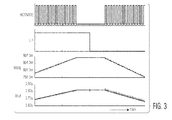
- Fig. 3 shows some examples of signals of the current source circuit 200 depicted in Fig. 2 .
- Fig. 3 shows the digital input signals, "activate” and “up,” which are provided to the digital controller 220 and the voltage signal, "V big ,” and the output current signal, “I out .”
- the voltage signal, “V big ,” and the current signal, “I out ” gradually increase 15 times, when the digital control signal, "up,” is set to 1 during 15 rising edges of the digital activation signal, “activate.”
- the voltage signal, “V big ,” and the current signal, “I out ,” remain unchanged, when the digital activation signal, "activate,” is set to 0.
- the output voltage, “V big ,” and the output current signal, “I out ,” gradually decrease 15 times, when the digital control signal, "up,” is set to 0 during 15 rising edges of the input signal, activate.
- the digital controller 202 sets the control signal, "prechrgp,” to 0 V when the output current, "I out ,” needs to be increased. Setting the control signal, “prechrgp,” to 0 V activates the transistor, M2, which charges a capacitor, "C1,” to a voltage of Vdd.
- the capacitor, C1 can be "parasitic” capacitance of the transistors, M2, M3, or implemented as a dedicated capacitor.
- the digital controller changes the control signal, "prechargp,” to the voltage, Vdd, which deactivates the transistor, M2.
- the digital controller sets the control signal, "CurUp,” to 0 V, which activates the transistor, M3, in order to redistribute the electric charges on the capacitors, C big , and, C1.
- the electric charge across the capacitors, C1, and C big is redistributed in a way that the voltage, "V big ,” across the capacitor, C big , and the output current, "I out ,” slightly increase.
- the current change step size i.e., current change pace
- the digital controller sets the control signal, "prechrgn,” to 0 V when the output current, "I out ,” needs to be decreased. Setting the control signal, “prechrgn,” to 0 V activates the transistor. M5, which discharges a capacitor, "C2.”
- the capacitor, C2 can be "parasitic” capacitance of the transistors, M4, and M5, or implemented as a dedicated capacitor. To transfer some of the electric charge on the capacitor, C big , to the capacitor, C2, the digital controller changes the control signal, "prechrgn,” to 0V, which deactivates the transistor, M5.
- the digital controller sets the control signal, "CurDown,” to 0V, which activates the transistor, M4, in order to redistribute the electric charges on the capacitors, C big , and C2.
- the electric charge across the capacitors, C big , and, C2 are redistributed in a way that the voltage, "V big ,” across the capacitor, C big , and the output current, "I out ,” slightly decrease.
- the current change step size i.e., current change pace
- Fig. 4 is a flow chart that illustrates an exemplary operation of the digital controller 202 depicted in Fig. 2 .
- control signals, "prechrgp,” and “CurUp” control the PMOS transistors, M1, M2, such that a value of '0' activates the PMOS transistors, M2, M3, while control signals “prechrgn,” and “CurDown,” control the NMOS switches, M4, M5, such that a value of '1' activates the NMOS transistors, M4, M5.
- a value of'-' means that a signal has a value of either '1' or '0.
- the digital controller begins operation at a neutral state in which the signal, "CurUp,” is set to '1,' the signal, “CurDown,” is set to '0,' and the control signals, "prechrgp,” and “CurUp,” are set to either '1' or '0,' at step 400.
- the digital controller determines the value of the signal, "up,” at step 402.
- the digital controller changes the state of the signal, "prechrgp,” at a rising edge of the input signal, “activate,” at step 404, and, subsequently, changes the state of the signal, "CurUp,” at step 406. If the signal, “up,” is at 0, the digital controller changes the state of the signal, “prechrgn,” at a rising edge of the input signal, “activate,” at step 408 and, subsequently, changes the state of the signal, "CurDown,” at step 410. The digital controller goes back to the neutral state either after a predefined delay time or after a falling edge of the signal, "activate.”
- the digital controller 202 depicted in Fig. 2 is implemented using one or more inverters and one or more plural-input single-output non-sequential logic devices.
- Fig. 5 depicts an embodiment of the digital controller depicted in Fig. 2 that is implemented by standard Boolean gates.
- a digital controller 502 includes two inverters, "G1", “G2,” with inverter delays, an AND gate, "G3,” two NAND gates, "G4,” “G5,” and two AND gates (each with one inverting input and one non-inverting input), "G6,” “G7.”
- the digital controller depicted in Fig. 5 is one possible embodiment of the digital controller depicted in Fig. 2 .
- the digital controller depicted in Fig. 2 is not limited to the embodiment shown in Fig. 5 .
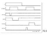
- Fig. 6 shows some examples of input signals and output signals of the digital controller 502 depicted in Fig. 5 .
- Fig. 6 shows the input digital signals, "activate,” “up,” and the output signals, "prechrgp,” “CurUp,” “CurDown,” “prechrgn,” of the digital controller.
- the digital controller enters an active state after a rising edge of the digital activation signal, "activate,” and sets the control signal, "prechrgp,” to 0V. Subsequently, the digital controller sets the control signal, "CurUp,” to 0V.
- the digital controller enters a neutral state after a falling edge of the digital activation signal, "activate,” and re-enters the active state after another rising edge of the digital activation signal, “activate.” Specifically, the digital controller sets the control signal, "prechrgn,” to a positive voltage, and subsequently, sets the control signal, "CurDown,” to a positive voltage.
- a current source circuit 700 includes a digital controller 702 that is controlled by the signals, "UP,” and “DN,” and the current generation circuit 204.
- the electric charge on the capacitor, C big can be varied by the signals, "UP,” and "DN.”
- the transistors, M2, M3, M4, M5, either take away charge (the amount being proportional to the ratio of C2/Cbig) from the capacitor, C big , or add charge (the amount being proportional to the ratio of C1/Cbig) to the capacitor, C big , thereby changing the output current, "I out .”
- the digital controller 702 sets the control signal, "prechrgp,” to 0 V in response to a surge in the signal, "DN,” (i.e., when less output current is needed) thereby activating the transistor, M2, which charges the capacitor, C1, (which can be implicitly present as “parasitic” capacitance of transistors, M2 and M3, or as a separate device) to a positive voltage of Vdd.
- the signal, "prechrgp” returns to the neutral setting of Vdd by inactivating (i.e. turning off) the transistor, M2, after which transistor, M3, is activated (i.e.
- the digital controller sets the control signal, "prechrgn,” to a positive voltage of Vdd in response to a dip in the signal, "UP,” (i.e., when more output current is needed) thereby activating (i.e. turning on) the transistor, M4, which discharges the voltage on the capacitor, C big , to the capacitor, C2, (which can be implicitly present as "parasitic” capacitance of transistors, M4 and M5, or as a separate device).
- the current source circuit 200 can be used to replace a digital-to-analog converter (DAC) in a DC offset cancellation circuit.
- DAC digital-to-analog converter
- a DAC is typically inserted in an analog signal processing chain to counter the effect of DC offset in amplifier circuits that can cause distortion or even signal clipping.
- reaching the desired combination of accuracy and range of the DAC typically increases design complexity on the one hand and significantly increases silicon area on the other.
- the control algorithm of the DAC may require strict monotonicity of the DAC input-output relation.
- a thermometer coded DAC with accompanying binary-to-thermometer coder is employed to solve the monotonicity requirement by design, which again introduces design complexity.
- the current source circuit 200 can be used in analog signal processing chains to cancel an unwanted DC element without these undesirable effects.
- Fig. 8 depicts an embodiment of a DC offset cancellation circuit 850 that includes the current source circuit 200 depicted in Fig. 2 .
- the digitally controlled current source circuit can remove the DC offset in a DC feedback loop 810 of the DC offset cancellation circuit.
- the current source circuit uses relative control inputs (e.g., up and down) rather than an absolute one as in a DAC. Consequently, the range of the DC offset cancellation circuit is decoupled from the accuracy (step size) of the DC offset cancellation circuit.
- DAC digital-to-analog converter
- the DC offset cancellation circuit includes a DC blocker 820, an amplifier circuit, "A1,” with DC offset, and the DC offset cancellation feedback loop 810, which includes an amplifier circuit, "A2,” an analog-to-digital converter (ADC) 822, a digital signal processor (DSP) 824, and the current source circuit 200.
- the DC offset cancellation circuit is used in a smartcard, such as a contactless smartcard.
- the power source circuit 100 depicted in Fig. 1 is a voltage source circuit that is used to generate an output voltage.
- Fig. 9 depicts an embodiment of the power source circuit 100 depicted in Fig. 1 that is used to generate an output voltage, "V out .”
- a voltage source circuit 900 includes a voltage generation circuit 904 and the digital controller 202.
- a difference between the voltage source circuit 900 and the current source circuit 200 is that the voltage source circuit 900 does not include the transistor, M1, which is used to generate the output current signal, "I out ,” in the current source circuit 200 of Fig. 2 .
- the voltage source circuit depicted in Fig. 9 is one possible embodiment of the power source circuit depicted in Fig. 1 .
- the power source circuit depicted in Fig. 1 is not limited to the embodiment shown in Fig. 9 .
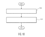
- Fig. 10 is a process flow diagram of a method for operating a power source circuit in accordance with an embodiment of the invention.
- the power source circuit may be similar to or the same as the power source circuit 100 depicted in Fig. 1 , the current source circuit 200 depicted in Fig. 2 , the current source circuit 700 depicted in Fig. 7 , and/or the voltage source circuit 900 depicted in Fig. 9 .
- At block 1002 at least one digital signal is received at the power source circuit from a feedback loop.
- output power signal of the power source circuit is increased or decreased an in response to the at least one digital signal.
- a current source circuit comprising a digital controller configured to receive a digital activation signal and a digital control signal from a feedback loop and a current generation circuit configured to increase or decrease an output current during a rising edge of the digital activation signal based on the Boolean value of the digital control signal, wherein the current generation circuit comprises a first type of switching devices, a second type of switching devices, and a capacitor connected to a node between the first type of switching devices and the second type of switching devices.
Landscapes
- Engineering & Computer Science (AREA)
- Power Engineering (AREA)
- Physics & Mathematics (AREA)
- Signal Processing (AREA)
- Computer Networks & Wireless Communication (AREA)
- Computer Hardware Design (AREA)
- Theoretical Computer Science (AREA)
- General Physics & Mathematics (AREA)
- Microelectronics & Electronic Packaging (AREA)
- Electromagnetism (AREA)
- Dc Digital Transmission (AREA)
- Dc-Dc Converters (AREA)
- Amplifiers (AREA)
Priority Applications (1)
| Application Number | Priority Date | Filing Date | Title |
|---|---|---|---|
| US14/818,256 US9798338B2 (en) | 2014-08-04 | 2015-08-04 | Digitally controllable power source |
Applications Claiming Priority (1)
| Application Number | Priority Date | Filing Date | Title |
|---|---|---|---|
| US14/133,267 US9426003B2 (en) | 2013-12-18 | 2013-12-18 | Proximity integrated circuit card bias adjustment |
Publications (3)
| Publication Number | Publication Date |
|---|---|
| EP2887273A2 true EP2887273A2 (de) | 2015-06-24 |
| EP2887273A3 EP2887273A3 (de) | 2015-11-11 |
| EP2887273B1 EP2887273B1 (de) | 2017-02-22 |
Family
ID=51359266
Family Applications (2)
| Application Number | Title | Priority Date | Filing Date |
|---|---|---|---|
| EP14179647.4A Not-in-force EP2887273B1 (de) | 2013-12-18 | 2014-08-04 | Digital steuerbare Stromquelle |
| EP14192871.3A Active EP2887274B1 (de) | 2013-12-18 | 2014-11-12 | Arbeitspunkteinstellung für kontaktlose Chipkarte |
Family Applications After (1)
| Application Number | Title | Priority Date | Filing Date |
|---|---|---|---|
| EP14192871.3A Active EP2887274B1 (de) | 2013-12-18 | 2014-11-12 | Arbeitspunkteinstellung für kontaktlose Chipkarte |
Country Status (2)
| Country | Link |
|---|---|
| US (1) | US9426003B2 (de) |
| EP (2) | EP2887273B1 (de) |
Families Citing this family (3)
| Publication number | Priority date | Publication date | Assignee | Title |
|---|---|---|---|---|
| US9798338B2 (en) | 2014-08-04 | 2017-10-24 | Nxp B.V. | Digitally controllable power source |
| EP3101596B1 (de) | 2015-06-03 | 2018-04-25 | Nxp B.V. | Anpassbare vorspannungsabstimmung |
| CN105007102B (zh) * | 2015-08-18 | 2017-08-22 | 珠海市一微半导体有限公司 | 修正米勒编码信源解码电路及其解码方法 |
Family Cites Families (29)
| Publication number | Priority date | Publication date | Assignee | Title |
|---|---|---|---|---|
| US3727135A (en) * | 1971-04-27 | 1973-04-10 | Us Army | Adaptive code modulation improvement in digital code modulators |
| US4229703A (en) * | 1979-02-12 | 1980-10-21 | Varian Associates, Inc. | Zero reference and offset compensation circuit |
| JPS5676613A (en) * | 1979-11-29 | 1981-06-24 | Toshiba Corp | Automatic offset calibrating circuit for operational amplifier |
| US6426663B1 (en) * | 1996-03-04 | 2002-07-30 | Delphi Technologies, Inc. | Analog/digital feedback circuitry for minimizing DC offset variations in an analog signal |
| US5940447A (en) | 1996-08-30 | 1999-08-17 | Motorola, Inc. | Wireless powered communication device using power signal sampling and method |
| JP3514111B2 (ja) * | 1997-07-09 | 2004-03-31 | 株式会社デンソー | オフセット電圧補正回路 |
| US6466007B1 (en) * | 2000-08-14 | 2002-10-15 | Teradyne, Inc. | Test system for smart card and indentification devices and the like |
| US6680985B1 (en) * | 2000-08-15 | 2004-01-20 | Hughes Electronics Corporation | Adaptive quadrature amplitude modulation decoding system |
| US6657488B1 (en) * | 2001-07-03 | 2003-12-02 | Silicon Laboratories, Inc. | Offset correction and slicing level adjustment for amplifier circuits |
| DE10229459C1 (de) * | 2002-07-01 | 2003-11-13 | Texas Instruments Deutschland | Transponder |
| US7023817B2 (en) | 2003-03-11 | 2006-04-04 | Motorola, Inc. | Method and apparatus for source device synchronization in a communication system |
| US7026866B2 (en) * | 2003-03-28 | 2006-04-11 | Tripath Technology, Inc. | DC offset self-calibration system for a switching amplifier |
| JP4328705B2 (ja) | 2004-02-27 | 2009-09-09 | 均 北吉 | Rfidタグ装置 |
| JP2006023671A (ja) | 2004-07-09 | 2006-01-26 | Sharp Corp | 画像形成装置及びそれを用いた画像形成方法 |
| KR20130069853A (ko) * | 2005-05-19 | 2013-06-26 | 넥스테스트 시스템즈 코포레이션 | 스마트 카드들을 테스트하기 위한 시스템 및 방법 |
| WO2007012053A1 (en) * | 2005-07-20 | 2007-01-25 | Stmicroelectronics, S.R.L. | Apparatus and method for detecting communications from multiple sources |
| JP4313795B2 (ja) | 2005-09-30 | 2009-08-12 | 富士通マイクロエレクトロニクス株式会社 | 非接触タグ、非接触タグの制御方法 |
| US7691746B2 (en) | 2007-07-31 | 2010-04-06 | Hewlett-Packard Development Company, L.P. | Formation of silicon nitride layer on back side of substrate |
| DE102007036207B4 (de) * | 2007-08-02 | 2010-08-12 | Texas Instruments Deutschland Gmbh | ASK-Demodulator mit großem Dynamikbereich zur Verwendung in 13-MHz-RFID-Transponder |
| US7885359B2 (en) | 2007-08-15 | 2011-02-08 | Seiko Epson Corporation | Sampling demodulator for amplitude shift keying (ASK) radio receiver |
| JP5349842B2 (ja) * | 2008-05-30 | 2013-11-20 | 株式会社日立製作所 | 低オフセット入力回路およびそれを含む信号伝送システム |
| JP4377946B1 (ja) * | 2008-06-10 | 2009-12-02 | 株式会社東芝 | 復調装置 |
| JP4364297B1 (ja) | 2008-12-24 | 2009-11-11 | 株式会社東芝 | Ask復調回路、通信モジュール、通信装置およびask復調方法 |
| US8222944B2 (en) * | 2009-11-20 | 2012-07-17 | Electronics And Telecommunications Research Institute | DC offset cancellation circuit |
| KR20120025747A (ko) * | 2010-09-08 | 2012-03-16 | 한국전자통신연구원 | 맨체스터 서브캐리어 신호에 대한 수동형 rfid 리더 디지털 복조 장치 및 방법 |
| US20120083205A1 (en) | 2010-10-04 | 2012-04-05 | Qualcomm Incorporated | Nfc device having a differential input envelope detector |
| US9369120B2 (en) * | 2011-01-14 | 2016-06-14 | Infineon Technologies Ag | Detector circuit, transponder and method for detecting signal amplitudes |
| US9143200B2 (en) * | 2012-09-26 | 2015-09-22 | Qualcomm Incorporated | Apparatus and method of receiver architecture and low-complexity decoder for line-coded and amplitude-modulated signal |
| US9008230B2 (en) | 2013-01-08 | 2015-04-14 | Nxp B.V. | Receiver and method for near field communication |
-
2013
- 2013-12-18 US US14/133,267 patent/US9426003B2/en active Active
-
2014
- 2014-08-04 EP EP14179647.4A patent/EP2887273B1/de not_active Not-in-force
- 2014-11-12 EP EP14192871.3A patent/EP2887274B1/de active Active
Non-Patent Citations (1)
| Title |
|---|
| None |
Also Published As
| Publication number | Publication date |
|---|---|
| US9426003B2 (en) | 2016-08-23 |
| EP2887273B1 (de) | 2017-02-22 |
| EP2887273A3 (de) | 2015-11-11 |
| EP2887274A1 (de) | 2015-06-24 |
| US20150172080A1 (en) | 2015-06-18 |
| EP2887274B1 (de) | 2019-07-10 |
Similar Documents
| Publication | Publication Date | Title |
|---|---|---|
| CN107819468B (zh) | 自举开关电路 | |
| KR101894782B1 (ko) | 저잡음 저-드롭아웃 레귤레이터 | |
| EP2237425B1 (de) | Stromschaltungsanordnung | |
| US20120044004A1 (en) | Track and hold architecture with tunable bandwidth | |
| US20140077882A1 (en) | System and Method for a Programmable Gain Amplifier | |
| JP4358450B2 (ja) | 高電圧ディジタル/アナログ変換器内の低電圧cmosスイッチを切り換える方法および装置 | |
| US9847763B2 (en) | Self-regulated reference for switched capacitor circuit | |
| KR20050111526A (ko) | 샘플링 스위치 | |
| US9397682B2 (en) | Reference buffer with wide trim range | |
| JP2011166449A (ja) | トランスミッションゲート及び半導体装置 | |
| JP2016032292A (ja) | インターリーブ型アナログ・ディジタル変換器のためのサンプルホールド回路 | |
| US8810283B2 (en) | CMOS transistor linearization method | |
| EP2887273B1 (de) | Digital steuerbare Stromquelle | |
| CN113225083B (zh) | 自举开关电路 | |
| US9705524B2 (en) | R2R digital-to-analog converter circuit | |
| JP2025529181A (ja) | アナログデジタル変換器において段間の利得誤差を低減するための方法及び装置 | |
| EP2518900A1 (de) | Stromlenkschaltung mit Rückmeldung | |
| EP2654204B1 (de) | Aufhebung von Verzerrungen in analogen Schaltungen | |
| US9798338B2 (en) | Digitally controllable power source | |
| WO2010137095A1 (ja) | 抵抗型デジタル/アナログ変換器 | |
| US10812059B2 (en) | Comparator | |
| US20170141767A1 (en) | Buffer circuit and voltage generator using the same | |
| KR20070088563A (ko) | 신규한 클럭 승압 방식을 사용하는 저전압 cmos 스위치 | |
| JP5688586B2 (ja) | コンパレータシステム、アナログデジタルコンバータおよびコンパレータの閾値補正方法。 | |
| EP3514964A1 (de) | Schaltung mit integriertem halbeiter |
Legal Events
| Date | Code | Title | Description |
|---|---|---|---|
| PUAI | Public reference made under article 153(3) epc to a published international application that has entered the european phase |
Free format text: ORIGINAL CODE: 0009012 |
|
| 17P | Request for examination filed |
Effective date: 20140804 |
|
| AK | Designated contracting states |
Kind code of ref document: A2 Designated state(s): AL AT BE BG CH CY CZ DE DK EE ES FI FR GB GR HR HU IE IS IT LI LT LU LV MC MK MT NL NO PL PT RO RS SE SI SK SM TR |
|
| AX | Request for extension of the european patent |
Extension state: BA ME |
|
| PUAL | Search report despatched |
Free format text: ORIGINAL CODE: 0009013 |
|
| AK | Designated contracting states |
Kind code of ref document: A3 Designated state(s): AL AT BE BG CH CY CZ DE DK EE ES FI FR GB GR HR HU IE IS IT LI LT LU LV MC MK MT NL NO PL PT RO RS SE SI SK SM TR |
|
| AX | Request for extension of the european patent |
Extension state: BA ME |
|
| RIC1 | Information provided on ipc code assigned before grant |
Ipc: H04L 27/00 20060101ALI20151007BHEP Ipc: G06K 19/07 20060101ALI20151007BHEP Ipc: H03F 1/30 20060101ALI20151007BHEP Ipc: H04L 25/06 20060101ALI20151007BHEP Ipc: H04L 27/06 20060101ALI20151007BHEP Ipc: G06K 19/077 20060101AFI20151007BHEP |
|
| R17P | Request for examination filed (corrected) |
Effective date: 20160511 |
|
| RBV | Designated contracting states (corrected) |
Designated state(s): AL AT BE BG CH CY CZ DE DK EE ES FI FR GB GR HR HU IE IS IT LI LT LU LV MC MK MT NL NO PL PT RO RS SE SI SK SM TR |
|
| RIC1 | Information provided on ipc code assigned before grant |
Ipc: G06K 19/077 20060101AFI20160916BHEP Ipc: H04L 25/06 20060101ALI20160916BHEP Ipc: H03F 1/30 20060101ALI20160916BHEP Ipc: H04L 27/06 20060101ALI20160916BHEP Ipc: H04L 27/00 20060101ALI20160916BHEP Ipc: G06K 19/07 20060101ALI20160916BHEP |
|
| GRAP | Despatch of communication of intention to grant a patent |
Free format text: ORIGINAL CODE: EPIDOSNIGR1 |
|
| INTG | Intention to grant announced |
Effective date: 20161028 |
|
| STAA | Information on the status of an ep patent application or granted ep patent |
Free format text: STATUS: GRANT OF PATENT IS INTENDED |
|
| GRAS | Grant fee paid |
Free format text: ORIGINAL CODE: EPIDOSNIGR3 |
|
| GRAA | (expected) grant |
Free format text: ORIGINAL CODE: 0009210 |
|
| STAA | Information on the status of an ep patent application or granted ep patent |
Free format text: STATUS: THE PATENT HAS BEEN GRANTED |
|
| AK | Designated contracting states |
Kind code of ref document: B1 Designated state(s): AL AT BE BG CH CY CZ DE DK EE ES FI FR GB GR HR HU IE IS IT LI LT LU LV MC MK MT NL NO PL PT RO RS SE SI SK SM TR |
|
| REG | Reference to a national code |
Ref country code: GB Ref legal event code: FG4D |
|
| REG | Reference to a national code |
Ref country code: CH Ref legal event code: EP |
|
| REG | Reference to a national code |
Ref country code: AT Ref legal event code: REF Ref document number: 869785 Country of ref document: AT Kind code of ref document: T Effective date: 20170315 |
|
| REG | Reference to a national code |
Ref country code: IE Ref legal event code: FG4D |
|
| REG | Reference to a national code |
Ref country code: DE Ref legal event code: R096 Ref document number: 602014006868 Country of ref document: DE |
|
| REG | Reference to a national code |
Ref country code: LT Ref legal event code: MG4D |
|
| REG | Reference to a national code |
Ref country code: NL Ref legal event code: MP Effective date: 20170222 |
|
| REG | Reference to a national code |
Ref country code: AT Ref legal event code: MK05 Ref document number: 869785 Country of ref document: AT Kind code of ref document: T Effective date: 20170222 |
|
| PG25 | Lapsed in a contracting state [announced via postgrant information from national office to epo] |
Ref country code: FI Free format text: LAPSE BECAUSE OF FAILURE TO SUBMIT A TRANSLATION OF THE DESCRIPTION OR TO PAY THE FEE WITHIN THE PRESCRIBED TIME-LIMIT Effective date: 20170222 Ref country code: NO Free format text: LAPSE BECAUSE OF FAILURE TO SUBMIT A TRANSLATION OF THE DESCRIPTION OR TO PAY THE FEE WITHIN THE PRESCRIBED TIME-LIMIT Effective date: 20170522 Ref country code: GR Free format text: LAPSE BECAUSE OF FAILURE TO SUBMIT A TRANSLATION OF THE DESCRIPTION OR TO PAY THE FEE WITHIN THE PRESCRIBED TIME-LIMIT Effective date: 20170523 Ref country code: LT Free format text: LAPSE BECAUSE OF FAILURE TO SUBMIT A TRANSLATION OF THE DESCRIPTION OR TO PAY THE FEE WITHIN THE PRESCRIBED TIME-LIMIT Effective date: 20170222 Ref country code: HR Free format text: LAPSE BECAUSE OF FAILURE TO SUBMIT A TRANSLATION OF THE DESCRIPTION OR TO PAY THE FEE WITHIN THE PRESCRIBED TIME-LIMIT Effective date: 20170222 |
|
| PG25 | Lapsed in a contracting state [announced via postgrant information from national office to epo] |
Ref country code: RS Free format text: LAPSE BECAUSE OF FAILURE TO SUBMIT A TRANSLATION OF THE DESCRIPTION OR TO PAY THE FEE WITHIN THE PRESCRIBED TIME-LIMIT Effective date: 20170222 Ref country code: SE Free format text: LAPSE BECAUSE OF FAILURE TO SUBMIT A TRANSLATION OF THE DESCRIPTION OR TO PAY THE FEE WITHIN THE PRESCRIBED TIME-LIMIT Effective date: 20170222 Ref country code: NL Free format text: LAPSE BECAUSE OF FAILURE TO SUBMIT A TRANSLATION OF THE DESCRIPTION OR TO PAY THE FEE WITHIN THE PRESCRIBED TIME-LIMIT Effective date: 20170222 Ref country code: LV Free format text: LAPSE BECAUSE OF FAILURE TO SUBMIT A TRANSLATION OF THE DESCRIPTION OR TO PAY THE FEE WITHIN THE PRESCRIBED TIME-LIMIT Effective date: 20170222 Ref country code: PT Free format text: LAPSE BECAUSE OF FAILURE TO SUBMIT A TRANSLATION OF THE DESCRIPTION OR TO PAY THE FEE WITHIN THE PRESCRIBED TIME-LIMIT Effective date: 20170622 Ref country code: BG Free format text: LAPSE BECAUSE OF FAILURE TO SUBMIT A TRANSLATION OF THE DESCRIPTION OR TO PAY THE FEE WITHIN THE PRESCRIBED TIME-LIMIT Effective date: 20170522 Ref country code: ES Free format text: LAPSE BECAUSE OF FAILURE TO SUBMIT A TRANSLATION OF THE DESCRIPTION OR TO PAY THE FEE WITHIN THE PRESCRIBED TIME-LIMIT Effective date: 20170222 Ref country code: AT Free format text: LAPSE BECAUSE OF FAILURE TO SUBMIT A TRANSLATION OF THE DESCRIPTION OR TO PAY THE FEE WITHIN THE PRESCRIBED TIME-LIMIT Effective date: 20170222 |
|
| PG25 | Lapsed in a contracting state [announced via postgrant information from national office to epo] |
Ref country code: EE Free format text: LAPSE BECAUSE OF FAILURE TO SUBMIT A TRANSLATION OF THE DESCRIPTION OR TO PAY THE FEE WITHIN THE PRESCRIBED TIME-LIMIT Effective date: 20170222 Ref country code: IT Free format text: LAPSE BECAUSE OF FAILURE TO SUBMIT A TRANSLATION OF THE DESCRIPTION OR TO PAY THE FEE WITHIN THE PRESCRIBED TIME-LIMIT Effective date: 20170222 Ref country code: SK Free format text: LAPSE BECAUSE OF FAILURE TO SUBMIT A TRANSLATION OF THE DESCRIPTION OR TO PAY THE FEE WITHIN THE PRESCRIBED TIME-LIMIT Effective date: 20170222 Ref country code: RO Free format text: LAPSE BECAUSE OF FAILURE TO SUBMIT A TRANSLATION OF THE DESCRIPTION OR TO PAY THE FEE WITHIN THE PRESCRIBED TIME-LIMIT Effective date: 20170222 Ref country code: CZ Free format text: LAPSE BECAUSE OF FAILURE TO SUBMIT A TRANSLATION OF THE DESCRIPTION OR TO PAY THE FEE WITHIN THE PRESCRIBED TIME-LIMIT Effective date: 20170222 |
|
| REG | Reference to a national code |
Ref country code: DE Ref legal event code: R097 Ref document number: 602014006868 Country of ref document: DE |
|
| PG25 | Lapsed in a contracting state [announced via postgrant information from national office to epo] |
Ref country code: DK Free format text: LAPSE BECAUSE OF FAILURE TO SUBMIT A TRANSLATION OF THE DESCRIPTION OR TO PAY THE FEE WITHIN THE PRESCRIBED TIME-LIMIT Effective date: 20170222 Ref country code: SM Free format text: LAPSE BECAUSE OF FAILURE TO SUBMIT A TRANSLATION OF THE DESCRIPTION OR TO PAY THE FEE WITHIN THE PRESCRIBED TIME-LIMIT Effective date: 20170222 Ref country code: PL Free format text: LAPSE BECAUSE OF FAILURE TO SUBMIT A TRANSLATION OF THE DESCRIPTION OR TO PAY THE FEE WITHIN THE PRESCRIBED TIME-LIMIT Effective date: 20170222 |
|
| PLBE | No opposition filed within time limit |
Free format text: ORIGINAL CODE: 0009261 |
|
| STAA | Information on the status of an ep patent application or granted ep patent |
Free format text: STATUS: NO OPPOSITION FILED WITHIN TIME LIMIT |
|
| 26N | No opposition filed |
Effective date: 20171123 |
|
| PG25 | Lapsed in a contracting state [announced via postgrant information from national office to epo] |
Ref country code: SI Free format text: LAPSE BECAUSE OF FAILURE TO SUBMIT A TRANSLATION OF THE DESCRIPTION OR TO PAY THE FEE WITHIN THE PRESCRIBED TIME-LIMIT Effective date: 20170222 |
|
| REG | Reference to a national code |
Ref country code: CH Ref legal event code: PL |
|
| PG25 | Lapsed in a contracting state [announced via postgrant information from national office to epo] |
Ref country code: MC Free format text: LAPSE BECAUSE OF FAILURE TO SUBMIT A TRANSLATION OF THE DESCRIPTION OR TO PAY THE FEE WITHIN THE PRESCRIBED TIME-LIMIT Effective date: 20170222 |
|
| PG25 | Lapsed in a contracting state [announced via postgrant information from national office to epo] |
Ref country code: CH Free format text: LAPSE BECAUSE OF NON-PAYMENT OF DUE FEES Effective date: 20170831 Ref country code: LI Free format text: LAPSE BECAUSE OF NON-PAYMENT OF DUE FEES Effective date: 20170831 |
|
| REG | Reference to a national code |
Ref country code: FR Ref legal event code: ST Effective date: 20180430 |
|
| REG | Reference to a national code |
Ref country code: IE Ref legal event code: MM4A |
|
| REG | Reference to a national code |
Ref country code: BE Ref legal event code: MM Effective date: 20170831 |
|
| PG25 | Lapsed in a contracting state [announced via postgrant information from national office to epo] |
Ref country code: LU Free format text: LAPSE BECAUSE OF NON-PAYMENT OF DUE FEES Effective date: 20170804 |
|
| PG25 | Lapsed in a contracting state [announced via postgrant information from national office to epo] |
Ref country code: IE Free format text: LAPSE BECAUSE OF NON-PAYMENT OF DUE FEES Effective date: 20170804 |
|
| PG25 | Lapsed in a contracting state [announced via postgrant information from national office to epo] |
Ref country code: BE Free format text: LAPSE BECAUSE OF NON-PAYMENT OF DUE FEES Effective date: 20170831 Ref country code: FR Free format text: LAPSE BECAUSE OF NON-PAYMENT OF DUE FEES Effective date: 20170831 |
|
| PG25 | Lapsed in a contracting state [announced via postgrant information from national office to epo] |
Ref country code: MT Free format text: LAPSE BECAUSE OF NON-PAYMENT OF DUE FEES Effective date: 20170804 |
|
| GBPC | Gb: european patent ceased through non-payment of renewal fee |
Effective date: 20180804 |
|
| PG25 | Lapsed in a contracting state [announced via postgrant information from national office to epo] |
Ref country code: HU Free format text: LAPSE BECAUSE OF FAILURE TO SUBMIT A TRANSLATION OF THE DESCRIPTION OR TO PAY THE FEE WITHIN THE PRESCRIBED TIME-LIMIT; INVALID AB INITIO Effective date: 20140804 |
|
| PG25 | Lapsed in a contracting state [announced via postgrant information from national office to epo] |
Ref country code: CY Free format text: LAPSE BECAUSE OF FAILURE TO SUBMIT A TRANSLATION OF THE DESCRIPTION OR TO PAY THE FEE WITHIN THE PRESCRIBED TIME-LIMIT Effective date: 20170222 Ref country code: GB Free format text: LAPSE BECAUSE OF NON-PAYMENT OF DUE FEES Effective date: 20180804 |
|
| PG25 | Lapsed in a contracting state [announced via postgrant information from national office to epo] |
Ref country code: MK Free format text: LAPSE BECAUSE OF FAILURE TO SUBMIT A TRANSLATION OF THE DESCRIPTION OR TO PAY THE FEE WITHIN THE PRESCRIBED TIME-LIMIT Effective date: 20170222 |
|
| PG25 | Lapsed in a contracting state [announced via postgrant information from national office to epo] |
Ref country code: TR Free format text: LAPSE BECAUSE OF FAILURE TO SUBMIT A TRANSLATION OF THE DESCRIPTION OR TO PAY THE FEE WITHIN THE PRESCRIBED TIME-LIMIT Effective date: 20170222 |
|
| PG25 | Lapsed in a contracting state [announced via postgrant information from national office to epo] |
Ref country code: AL Free format text: LAPSE BECAUSE OF FAILURE TO SUBMIT A TRANSLATION OF THE DESCRIPTION OR TO PAY THE FEE WITHIN THE PRESCRIBED TIME-LIMIT Effective date: 20170222 Ref country code: IS Free format text: LAPSE BECAUSE OF FAILURE TO SUBMIT A TRANSLATION OF THE DESCRIPTION OR TO PAY THE FEE WITHIN THE PRESCRIBED TIME-LIMIT Effective date: 20170622 |
|
| P01 | Opt-out of the competence of the unified patent court (upc) registered |
Effective date: 20230725 |
|
| PGFP | Annual fee paid to national office [announced via postgrant information from national office to epo] |
Ref country code: DE Payment date: 20240723 Year of fee payment: 11 |
|
| REG | Reference to a national code |
Ref country code: DE Ref legal event code: R119 Ref document number: 602014006868 Country of ref document: DE |