EP2883239B1 - Verfahren zur herstellung eines halbleiterbauelements - Google Patents
Verfahren zur herstellung eines halbleiterbauelements Download PDFInfo
- Publication number
- EP2883239B1 EP2883239B1 EP13802420.3A EP13802420A EP2883239B1 EP 2883239 B1 EP2883239 B1 EP 2883239B1 EP 13802420 A EP13802420 A EP 13802420A EP 2883239 B1 EP2883239 B1 EP 2883239B1
- Authority
- EP
- European Patent Office
- Prior art keywords
- layer
- electrode
- semiconductor substrate
- etching
- metal layer
- Prior art date
- Legal status (The legal status is an assumption and is not a legal conclusion. Google has not performed a legal analysis and makes no representation as to the accuracy of the status listed.)
- Not-in-force
Links
Images



Classifications
-
- H—ELECTRICITY
- H10—SEMICONDUCTOR DEVICES; ELECTRIC SOLID-STATE DEVICES NOT OTHERWISE PROVIDED FOR
- H10D—INORGANIC ELECTRIC SEMICONDUCTOR DEVICES
- H10D64/00—Electrodes of devices having potential barriers
- H10D64/01—Manufacture or treatment
- H10D64/011—Manufacture or treatment of electrodes ohmically coupled to a semiconductor
- H10D64/0111—Manufacture or treatment of electrodes ohmically coupled to a semiconductor to Group IV semiconductors
- H10D64/0115—Manufacture or treatment of electrodes ohmically coupled to a semiconductor to Group IV semiconductors to silicon carbide
-
- H—ELECTRICITY
- H10—SEMICONDUCTOR DEVICES; ELECTRIC SOLID-STATE DEVICES NOT OTHERWISE PROVIDED FOR
- H10P—GENERIC PROCESSES OR APPARATUS FOR THE MANUFACTURE OR TREATMENT OF DEVICES COVERED BY CLASS H10
- H10P50/00—Etching of wafers, substrates or parts of devices
- H10P50/20—Dry etching; Plasma etching; Reactive-ion etching
- H10P50/26—Dry etching; Plasma etching; Reactive-ion etching of conductive or resistive materials
- H10P50/264—Dry etching; Plasma etching; Reactive-ion etching of conductive or resistive materials by chemical means
-
- H—ELECTRICITY
- H10—SEMICONDUCTOR DEVICES; ELECTRIC SOLID-STATE DEVICES NOT OTHERWISE PROVIDED FOR
- H10P—GENERIC PROCESSES OR APPARATUS FOR THE MANUFACTURE OR TREATMENT OF DEVICES COVERED BY CLASS H10
- H10P50/00—Etching of wafers, substrates or parts of devices
- H10P50/60—Wet etching
- H10P50/64—Wet etching of semiconductor materials
- H10P50/642—Chemical etching
Definitions
- the present invention relates to a semiconductor device and a manufacturing method of a semiconductor device.
- a technology has been developed in which a portion of an insulating layer formed on a surface of an silicon carbide (SiC) semiconductor substrate is removed by etching to form an opening and a metal electrode which forms an ohmic contact with the SiC semiconductor substrate is formed in the opening.
- SiC silicon carbide
- a silicon oxide film SiO 2 film
- a resist layer is next formed on a surface of the silicon oxide film.
- an opening is formed by patterning the resist layer.
- the silicon oxide film in an area exposed through the opening of the resist layer is next etched.
- the resist layer is then removed, and a metal (molybdenum) electrode layer is formed on the silicon oxide film and the surface of the SiC semiconductor layer.
- a resist layer is next formed on a surface of the metal electrode layer.
- the resist layer is then patterned, thereby forming a resist layer only on a portion to remain as an electrode.
- the metal electrode layer is next removed by etching, thereby allowing only the metal electrode layer protected by the resist layer to remain. Accordingly, the metal electrode is formed in the opening of the insulating layer.
- the metal electrode is formed in a whole area where the silicon oxide film (SiO 2 film) is removed on the SiC semiconductor substrate.
- sintering is performed in a state where the metal electrode and the silicon oxide film contact with each other.
- metal oxides may be generated in a reaction between the metal electrode and the silicon oxide film SiO 2 . This may increase a contact resistance between the SiC semiconductor substrate and the metal electrode.
- JP 2002-093742 A discloses a method of forming an ohmic electrode having a low contact resistance on a SiC substrate.
- the ohmic electrode is formed inside an opening in an insulating film.
- the gap between the electrode and the insulating film is controlled by etching the sidewalls of the opening before patterning the ohmic electrode in a lift-off process.
- the present invention provides a technology which can hinder an increase in contact resistance between an SiC substrate and an electrode metal layer.
- a manufacturing method of a semiconductor device the method being defined in claim 1. As a result, an increase in contact resistance between the SiC substrate and the electrode metal layer is hindered.
- a step of forming an electrode metal layer includes a step of forming an ohmic electrode layer by depositing a metal material which forms an ohmic contact with an SiC semiconductor substrate on a surface of the SiC semiconductor substrate and a surface of a resist layer.
- the step of forming the electrode metal layer includes a step of forming a protective metal layer by depositing a metal material which protects the ohmic electrode layer on a face side of the ohmic electrode layer after the ohmic electrode layer is formed.
- a step of etching is performed in a state where the protective metal layer is formed on the ohmic electrode layer. This hinders a surface (upper surface) of the ohmic electrode layer from being etched, thereby hindering excessive reduction in the dimension of the ohmic electrode layer. As a result, an increase in contact resistance between the ohmic electrode layer and the SiC semiconductor substrate can be hindered.
- the protective metal layer is not etched. Further, sintering is performed at a temperature not lower than a melting point of the protective metal layer.
- the etching may be wet etching which uses an etching solution.
- An etching rate of the etching solution for the protective metal layer may be lower than an etching rate of the etching solution for the insulating layer and lower than the etching rate of the etching solution for the ohmic electrode layer.
- the etching rates of the etching solution for the insulating layer, the ohmic electrode layer, and the protective metal layer are adjusted, thereby enabling the etching step by wet etching that is a simple method.
- the step of forming the electrode metal layer may further include a step of forming a carbon adsorbing metal layer by depositing a metal material which adsorbs carbon on a surface of the ohmic electrode layer between the step of forming the ohmic electrode layer and the step of forming the protective metal layer.
- the carbon adsorbing metal layer is formed between the ohmic electrode layer and the protective metal layer.
- the carbon adsorbing metal layer can adsorb byproduct carbon (C) generated in a reaction between the ohmic electrode layer and silicon in the insulating layer.
- C byproduct carbon
- the semiconductor device disclosed in the present application includes: an SiC semiconductor substrate; an insulating layer arranged on a surface of the SiC semiconductor substrate and having an opening for exposing a portion of the surface of the SiC semiconductor substrate; an ohmic electrode layer arranged in the opening of the insulating layer and forming an ohmic contact with the surface of the SiC semiconductor substrate; a carbon adsorbing metal layer arranged on a surface of the ohmic electrode layer in the opening of the insulating layer; and a protective metal layer arranged on a surface of the carbon adsorbing metal layer, the surface of the ohmic electrode layer, side surfaces of the carbon adsorbing metal layer in the opening of the insulating layer.
- the carbon adsorbing metal layer adsorbs carbon (C), and the protective metal layer prevents the ohmic electrode metal layer from contacting with the insulating layer. As a result, an ohmic electrode having low contact resistance is realized.
- the semiconductor device 1 is a vertical MOSFET.
- the semiconductor device 1 includes a drain electrode 2, an SiC semiconductor substrate 4, insulating layers 6, 7, a source electrode 10, and an aluminum vapor deposition layer 8.
- the drain electrode 2 is formed of aluminum or the like.
- a drain electrode 2 forms an ohmic contact with a lower surface of the SiC semiconductor substrate 4.
- the SiC semiconductor substrate 4 is formed of silicon carbide (SiC) as a material.
- a drain region 14 containing N + type impurity is formed in a lowermost layer (a layer above the drain electrode 2) of the SiC semiconductor substrate 4.
- a drift region 18 containing N type impurity is formed on the drain region 14.
- a base region 20 containing P type impurity is formed on the drift region 18.
- a source region 22 containing N + type impurity is selectively formed in the base region 20.
- a trench 30 (groove) is formed in an upper surface of the SiC semiconductor substrate 4.
- the trench 30 passes through the source region 22 and the base region 20.
- the trench 30 has a lower end that reaches the drift region 18 and is formed in such a depth that does not reach the drain region 14.
- a gate insulating film 26 formed of silicon oxide is formed on an inner wall of the trench 30.
- a gate electrode 24 is embedded inside the gate insulating film 26. Polysilicon is used for the gate electrode 24, for example.
- the gate electrode 24 is opposed to the source region 22, the base region 20, and the drift region 18 via the gate insulating film 26.
- a cap insulating layer 6 is formed on the upper surface of the SiC semiconductor substrate 4.
- the cap insulating layer 6 covers an upper surface of the gate electrode 24.
- the cap insulating layer 6 insulates the gate electrode 24 from the aluminum vapor deposition layer 8.
- An interlayer insulating layer 7 is further formed on the surface of the SiC semiconductor substrate 4.
- a gap is provided between the interlayer insulating layer 7 and the cap insulating layer 6, and a source electrode 10 is formed therebetween.
- the source electrode 10 is formed on both sides between which the cap insulating layer 6 is interposed.
- the aluminum vapor deposition layer 8 is formed in an uppermost layer of the SiC semiconductor substrate 4 to cover the cap insulating layer 6, the interlayer insulating layer 7, and the gate electrode 24.
- the source electrode 10 is formed between the cap insulating layer 6 and the interlayer insulating layer 7.
- the source electrode 10 includes an ohmic electrode layer 52, a carbon adsorbing metal layer 54, and a protective metal layer 56.
- the carbon adsorbing metal layer 54 is formed on the ohmic electrode layer 52.
- the protective metal layer 56 is formed on an upper surface and side surfaces of the carbon adsorbing metal layer 54 and side surfaces of the ohmic electrode layer 52.
- the ohmic electrode layer 52 is a layer in a lowermost position of the source electrode 10 (a layer positioned above the SiC semiconductor substrate 4).
- the ohmic electrode layer 52 forms an ohmic contact with the SiC semiconductor substrate 4.
- a silicide layer 62 is formed in an interface between the ohmic electrode layer 52 and the SiC semiconductor substrate 4.
- At least one kind of metal selected from the group consisting of nickel (Ni), titanium (Ti), and aluminum (Al) may be used for the ohmic electrode layer 52, for example.
- nickel (Ni) is used.
- At least one kind of metal selected from the group consisting of iron (Fe), tungsten (W), and titanium (Ti) may be used for the carbon adsorbing metal layer 54, for example. In this embodiment, iron (Fe) is used.
- At least one kind of metal selected from the group consisting of gold (Au), silver (Ag), and platinum (Pt) may be used for the protective metal layer 56, for example.
- gold (Au) is used.
- the protective metal layer 56 is formed to cover an upper side and side surfaces of a metal layer in which the ohmic electrode layer 52 and the carbon adsorbing metal layer 54 are stacked. Gaps are formed between the protective metal layer 56 and the cap insulating layer 6 and between the protective metal layer 56 and the interlayer insulating layer 7.
- a manufacturing method of the semiconductor device 1 of this embodiment will be described hereinafter.
- a conventional method can be used except a manufacturing method of the source electrode 10, and descriptions will thus be omitted.
- a manufacturing method of peripheral portions of the source electrode 10 will be described.
- the source electrode 10 is formed after the drain region 14, the drift region 18, the base region 20, the source region 22, the gate electrode 24, and the like are formed in the SiC semiconductor substrate 4 and in peripheral portions thereof. However, those regions are not shown in FIGs. 1 to 8 .
- the insulating layer 5 formed of silicon oxide (SiO 2 ) is first formed on the surface of the SiC semiconductor substrate 4.
- the insulating layer 5 can be formed by a known method (for example, CVD or the like).
- the thickness of the insulating layer 5 may be set to 1.5 ⁇ m, for example.
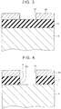
- a resist layer is formed on a whole surface of the insulating layer 5 by spin coating or the like, and the resist layer is patterned, thereby forming a resist mask 40 ( FIG. 3 ).
- the resist mask 40 has an opening 41 corresponding to the size of the formed gate electrode 24.
- the insulating layer 5 in an area exposed through an opening 41 of the resist mask 40 is next removed by dry etching.
- the insulating layer 5 positioned in the opening 41 of the resist mask 40 is removed, thereby exposing the SiC semiconductor substrate 4 inside the opening 41.
- the width of the opening 41 in the transverse direction of the figure may be set to two ⁇ m, for example.
- a portion of the insulating layer 5 is removed, and the cap insulating layer 6, and the interlayer insulating layer 7 are thereby formed.
- Electrode metal layer formation step and ohmic electrode layer formation step Electrode metal layer formation step and ohmic electrode layer formation step
- Ni layer 52 is the ohmic electrode layer 52 which forms an ohmic contact with the SiC semiconductor substrate 4 by sintering, as described below.
- the thickness of the Ni layer 52 may be set to 50 nm, for example.
- Fe layer 54 is formed on a whole surface of the Ni layer 52. Therefore, the Fe layer 54 is formed above the resist mask 40.
- the Fe layer 54 becomes austenite by the sintering described below and serves as a carbon adsorbing layer which adsorbs carbon (C).
- the thickness of the Fe layer 54 may be set to 50 nm, for example.
- the Au layer 56 is formed on a whole surface of the Fe layer 54 and above the resist mask 40.
- the Au layer 56 is a protective metal layer which protects the Ni layer 52 and the Fe layer 54 in a side etching step described below.
- the thickness of the Au layer 56 may be set to 50 nm, for example.
- the resist mask 40 is next removed by use of an organic peeling agent ( FIG. 6 ). At this point, the Ni layer 52, the Fe layer 54, and the Au layer 56 that are vapor-deposited on the surface of the resist mask 40 are also removed. Accordingly, a metal layer in which the Ni layer 52, the Fe layer 54, and the Au layer 56 are stacked is formed in an area inside the opening 41 of the surface of the SiC semiconductor substrate 4.
- Dilute hydrofluoric acid can be used as an etching solution for wet etching, for example.
- the etching rates of the etching solution are high in the insulating layers 6, 7, the Ni layer 52, and the Fe layer 54 and low in the Au layer 56. Therefore, as shown in FIG. 7 , upper surfaces and side surfaces, which are in the opening 41, of the insulating layers 6, 7 are removed by the wet etching. The side surfaces of the insulating layers 6, 7 are removed, thereby increasing the width of the opening 41 (the gap between the insulating layer 6 and the insulating layer 7).
- the lengths of the etched side surfaces of the Ni layer 52 and the Fe layer 54 are preferably approximately 1.5 times (150 nm) of the sum of the thickness of the Ni layer 52 and the Fe layer 54.
- Sintering is next performed in which the SiC semiconductor substrate 4 is heated by a heating device ( FIG. 8 ).
- An infrared lamp RTA (Rapid Thermal Anneal) device (not shown) can be used as the heating device, for example.
- the heating device may be of an open-atmosphere type.
- the sintering is performed in a temperature range which is not lower than the melting point (1065°C) of the Au layer 56 and where the Fe layer 54 becomes austenite. A heating period is one minute, for example.
- the sintering allows the Ni layer 52 to react with the SiC semiconductor substrate 4, thereby forming nickel silicide 62 (Ni 2 Si).
- the nickel silicide 62 reduces the contact resistance between the Ni layer 52 and the SiC semiconductor substrate 4, thereby forming the ohmic contact between the Ni layer 52 and the SiC semiconductor substrate 4.
- the Au layer 56 which laterally protrudes with respect to the Ni layer 52 and the Fe layer 54 melts by the sintering. Accordingly, as shown in FIG. 8 , the melted Au layer 56 covers the side surfaces of the Ni layer 52 and the Fe layer 54. After the Au layer 56 melts, gaps are formed between the Au layer 56 and the cap insulating layer 6 and between the Au layer 56 and the interlayer insulating layer 7.
- the aluminum vapor deposition layer 8 is finally formed to cover the gate electrode 24, the cap insulating layer 6, and the interlayer insulating layer 7.
- the aluminum vapor deposition layer 8 is formed by vapor-depositing titanium (Ti) in a thickness of 500 nm by sputtering and vapor-depositing aluminum (Al) in a thickness of four ⁇ m thereon.
- Ti titanium
- Al aluminum
- the sintering is performed in a state where gaps are formed between the Ni layer 52 and the insulating layers (SiO 2 ) 6, 7.
- the Ni layer 52 does not contact with the insulating layer 6 or the insulating layer 7 during the sintering, generation of metal oxides (for example, nickel oxide (NiO)) is hindered.
- NiO nickel oxide
- the Au layer 56 covers an upper surface of the Fe layer 54. Accordingly, in the side etching step, the Ni layer 52 is removed from their lateral sides. In other words, etching of the Ni layer 52 from its upper surface is hindered. This hinders excessive etching of the Ni layer 52. As a result, an increase in contact resistance between the Ni layer 52 and the SiC semiconductor substrate 4 can be hindered.
- both of the Ni layer 52 and the Fe layer 54 that are positioned below the Au layer 56 are removed like their lateral sides are scooped. Accordingly, ends of the Au layer 56 laterally protrude with respect to the side surfaces of both of the Ni layer 52 and the Fe layer 54.
- the Au layer melts by the sintering step, thereby covering the side surfaces of both of the Ni layer 52 and the Fe layer 54.
- the Au layer 56 covers surfaces of portions of the Ni layer 52 and the Fe layer 54 that are exposed on the SiC semiconductor substrate 4. Accordingly, the Ni layer 52 contacts with the insulating layers (SiO 2 ) 6, 7 to generate metal oxides (for example, NiO), and an increase in contact resistance can thereby be hindered.
- the Au layer 56 covers the surfaces of the portions of the Ni layer 52 and the Fe layer 54 that are exposed on the SiC semiconductor substrate 4. This hinders the Ni layer 52 and the Fe layer 54 from being oxidized during the sintering. Accordingly, the sintering can be performed in an environment where oxygen is present. Therefore, a sintering device is not required to include an expensive vacuum mechanism, thereby reducing device cost. In addition, it is not required to perform purge for creating a vacuum in the sintering device, thereby allowing reduction in time required for the sintering.
- the Ni layer 52 reacts with silicon (Si) in the SiC semiconductor substrate 4, resulting in formation of nickel silicides (for example, Ni 2 Si).
- the Ni layer 52 reacts with silicon (Si) in the SiC semiconductor substrate 4, thus generating carbon (C) as a byproduct from the SiC semiconductor substrate 4.
- the byproduct carbon segregates to an interface or the like between the Ni layer 52 and the SiC semiconductor substrate 4, a byproduct layer is formed.
- the byproduct layer may increase the contact resistance between the SiC semiconductor substrate 4 and the Ni layer 52.
- the source electrode 10 includes the Fe layer 54.
- the Fe layer 54 has austenite or martensite in at least a portion thereof. Accordingly, the byproduct carbon generated from the SiC semiconductor substrate 4 can be dissolved in the Fe layer 54. Therefore, an increase in contact resistance between the SiC semiconductor substrate 4 and the Ni layer 52 due to deposition of carbon on the contact interface between the SiC semiconductor substrate 4 and the Ni layer 52 can be hindered.
- the Ni layer 52 is used as the ohmic electrode layer 52.
- titanium (Ti) or aluminum (Al) may be used as a material of the ohmic electrode layer 52.
- the protective metal layer 56 is formed of Au, but the present invention is not limited thereto.
- the protective metal layer 56 may be formed of silver (Ag) or platinum (Pt). In such a case, it is sufficient that the temperature of the sintering be not less than the melting point of silver (960°C) or the melting point of platinum (1770°C).
- the carbon adsorbing metal layer 54 is formed of Fe, but the present invention is not limited thereto.
- the carbon adsorbing metal layer 54 may be formed of tungsten (W) or titanium (Ti).
Landscapes
- Electrodes Of Semiconductors (AREA)
- Chemical & Material Sciences (AREA)
- Chemical Kinetics & Catalysis (AREA)
- General Chemical & Material Sciences (AREA)
- Bipolar Transistors (AREA)
Claims (3)
- Herstellungsverfahren einer Halbleitervorrichtung, wobei das Verfahren aufweist:Ausbilden einer Isolierschicht auf einer Oberfläche eines Halbleitersubstrats (4) aus Siliziumkarbid (SiC);Ausbilden einer Resistschicht (40) mit einer Öffnung auf einer Oberfläche der Isolierschicht;Entfernen der Isolierschicht in einem Bereich, der durch die Öffnung der Resistschicht (40) freiliegt;Ausbilden einer Elektroden-Metallschicht durch Ablagern von Metall als einem Elektrodenmaterial auf der Oberfläche des SiC-Halbleitersubstrats (4) und einer Oberfläche der Resistschicht in einem Zustand, bei dem die Resistschicht auf der Isolierschicht ausgebildet ist, nachdem die Isolierschicht entfernt wurde;Entfernen der Resistschicht (40), auf der die Elektroden-Metallschicht abgelagert ist, nachdem die Elektroden-Metallschicht ausgebildet wurde;Verbreitern einer Lücke zwischen einer Innenwandoberfläche einer Öffnung, die in der Isolierschicht ausgebildet ist, und der Elektroden-Metallschicht durch Ätzen der Isolierschicht, nachdem die Resistschicht (40) entfernt wurde; undAusbilden eines ohmischen Kontakts zwischen der Elektroden-Metallschicht und dem SiC-Halbleitersubstrat (4) durch Erwärmen des SiC-Halbleitersubstrats (4) und der Elektroden-Metallschicht, nachdem das Ätzen durchgeführt wurde, wobei das Ausbilden der Elektroden-Metallschicht beinhaltet:Ausbilden einer ohmischen Elektrodenschicht (52) durch Ablagern eines Metallmaterials, das einen ohmischen Kontakt mit dem SiC-Halbleitersubstrat (4) auf der Oberfläche des SiC-Halbleitersubstrats (4) und der Oberfläche der Resistschicht ausbildet; undAusbilden einer schützenden Metallschicht (56) durch Ablagern eines Metallmaterials, das die ohmische Elektrodenschicht (52) schützt, auf einer Stirnseite der ohmischen Elektrodenschicht (52), nachdem die ohmische Elektrodenschicht (52) ausgebildet wurde, und wobei bei dem Ätzen der Isolierschicht die Seitenwände der ohmischen Elektrodenschicht (52) weiter geätzt werden, wobei die schützende Metallschicht (56) nicht geätzt wird, und wobei das Erwärmen bei einer Temperatur durchgeführt wird, die nicht niedriger ist als ein Schmelzpunkt der schützenden Metallschicht (56).
- Verfahren einer Halbleitervorrichtung nach Anspruch 1, wobei das Ätzen ein Nassätzen ist, bei dem eine Ätzlösung verwendet wird, und
wobei eine Ätzrate der Ätzlösung für die schützende Metallschicht (56) niedriger ist als eine Ätzrate der Ätzlösung für die Isolierschicht und niedriger als eine Ätzrate der Ätzlösung für die ohmische Elektrodenschicht. - Verfahren einer Halbleitervorrichtung nach Anspruch 1 oder 2, ferner aufweisend das Ausbilden einer kohlenstoffadsorbierenden Metallschicht durch Ablagern eines Metallmaterials, das Kohlenstoff auf einer Oberfläche der ohmischen Elektrodenschicht zwischen dem Ausbilden der ohmischen Elektrodenschicht und dem Ausbilden der schützenden Metallschicht adsorbiert.
Applications Claiming Priority (2)
| Application Number | Priority Date | Filing Date | Title |
|---|---|---|---|
| JP2012231547A JP5838951B2 (ja) | 2012-10-19 | 2012-10-19 | 半導体装置及び半導体装置の製造方法 |
| PCT/IB2013/002112 WO2014060804A2 (en) | 2012-10-19 | 2013-09-24 | Semiconductor device and manufacturing method of semiconductor device |
Publications (3)
| Publication Number | Publication Date |
|---|---|
| EP2883239A2 EP2883239A2 (de) | 2015-06-17 |
| EP2883239B1 true EP2883239B1 (de) | 2017-10-25 |
| EP2883239B8 EP2883239B8 (de) | 2018-02-14 |
Family
ID=49726810
Family Applications (1)
| Application Number | Title | Priority Date | Filing Date |
|---|---|---|---|
| EP13802420.3A Not-in-force EP2883239B8 (de) | 2012-10-19 | 2013-09-24 | Verfahren zur herstellung eines halbleiterbauelements |
Country Status (6)
| Country | Link |
|---|---|
| US (1) | US9607836B2 (de) |
| EP (1) | EP2883239B8 (de) |
| JP (1) | JP5838951B2 (de) |
| CN (1) | CN104885194B (de) |
| TW (1) | TWI562369B (de) |
| WO (1) | WO2014060804A2 (de) |
Families Citing this family (1)
| Publication number | Priority date | Publication date | Assignee | Title |
|---|---|---|---|---|
| KR102452691B1 (ko) * | 2017-11-20 | 2022-10-11 | 현대자동차주식회사 | 전력반도체 소자 제조방법 및 전력반도체 소자 |
Family Cites Families (10)
| Publication number | Priority date | Publication date | Assignee | Title |
|---|---|---|---|---|
| JP4671314B2 (ja) * | 2000-09-18 | 2011-04-13 | 独立行政法人産業技術総合研究所 | オーミック電極構造体の製造方法、接合型fet又は接合型sitのオーミック電極構造体の製造方法、及び半導体装置の製造方法 |
| US6759683B1 (en) * | 2001-08-27 | 2004-07-06 | The United States Of America As Represented By The Secretary Of The Army | Formulation and fabrication of an improved Ni based composite Ohmic contact to n-SiC for high temperature and high power device applications |
| CN100537847C (zh) * | 2005-02-24 | 2009-09-09 | 关东化学株式会社 | 钛、铝金属层叠膜蚀刻液组合物 |
| JP2006332230A (ja) * | 2005-05-25 | 2006-12-07 | Ecotron:Kk | ショットキーバリアダイオード及びその製造方法 |
| JP2008227405A (ja) * | 2007-03-15 | 2008-09-25 | Toyota Motor Corp | n型4H−SiC基板上にオーミック電極を形成する方法 |
| DE102007029829A1 (de) * | 2007-06-28 | 2009-01-02 | Infineon Technologies Austria Ag | Halbleiterbauelement mit einem ohmschen Kontakt |
| JP5358584B2 (ja) * | 2008-10-23 | 2013-12-04 | 本田技研工業株式会社 | 電極、半導体装置、およびその製造方法 |
| JP2011176183A (ja) | 2010-02-25 | 2011-09-08 | Toyota Motor Corp | 半導体装置の製造方法 |
| JP2011204804A (ja) * | 2010-03-24 | 2011-10-13 | Toshiba Corp | 化合物半導体装置及びその製造方法 |
| JP5284389B2 (ja) * | 2011-03-07 | 2013-09-11 | 株式会社東芝 | 半導体装置 |
-
2012
- 2012-10-19 JP JP2012231547A patent/JP5838951B2/ja not_active Expired - Fee Related
-
2013
- 2013-09-24 WO PCT/IB2013/002112 patent/WO2014060804A2/en not_active Ceased
- 2013-09-24 US US14/417,902 patent/US9607836B2/en not_active Expired - Fee Related
- 2013-09-24 EP EP13802420.3A patent/EP2883239B8/de not_active Not-in-force
- 2013-09-24 CN CN201380040446.0A patent/CN104885194B/zh not_active Expired - Fee Related
- 2013-10-04 TW TW102136017A patent/TWI562369B/zh not_active IP Right Cessation
Non-Patent Citations (1)
| Title |
|---|
| None * |
Also Published As
| Publication number | Publication date |
|---|---|
| EP2883239A2 (de) | 2015-06-17 |
| CN104885194B (zh) | 2017-06-27 |
| JP5838951B2 (ja) | 2016-01-06 |
| JP2014086438A (ja) | 2014-05-12 |
| TWI562369B (en) | 2016-12-11 |
| WO2014060804A3 (en) | 2014-06-12 |
| EP2883239B8 (de) | 2018-02-14 |
| CN104885194A (zh) | 2015-09-02 |
| US20150214052A1 (en) | 2015-07-30 |
| WO2014060804A2 (en) | 2014-04-24 |
| TW201417296A (zh) | 2014-05-01 |
| US9607836B2 (en) | 2017-03-28 |
Similar Documents
| Publication | Publication Date | Title |
|---|---|---|
| CN103872103B (zh) | 用于碳化硅装置中欧姆接触的系统和方法 | |
| TWI307938B (en) | Method and process to make multiple-threshold metal_gates cmos technology | |
| CN105144382A (zh) | 制造集成结构的方法和形成垂直堆叠存储器单元的方法 | |
| JP5452876B2 (ja) | 半導体装置およびその製造方法 | |
| JP2006182781A5 (de) | ||
| JP4606525B2 (ja) | 半導体デバイス | |
| JP2012160485A (ja) | 半導体装置とその製造方法 | |
| US20240213336A1 (en) | Gate-all-around transistor, method for manufacturing the same, and semiconductor device | |
| US9704743B2 (en) | Method for manufacturing silicon carbide semiconductor device | |
| EP2883239B1 (de) | Verfahren zur herstellung eines halbleiterbauelements | |
| US8796123B2 (en) | Method of manufacturing silicon carbide semiconductor device | |
| JPS5830147A (ja) | 半導体装置 | |
| US7041585B2 (en) | Process for producing an integrated electronic component | |
| JP2010171327A (ja) | 半導体装置の製造方法 | |
| JP7663035B2 (ja) | 炭化珪素半導体装置およびその製造方法 | |
| JP7548232B2 (ja) | 炭化珪素半導体装置の製造方法及び炭化珪素半導体装置 | |
| CN116779652A (zh) | 使用二维材料提高性能的半导体开关器件 | |
| JP2021034400A (ja) | 半導体装置の製造方法 | |
| JP5181710B2 (ja) | 半導体装置の製造方法 | |
| JP4694846B2 (ja) | 半導体装置の製造方法 | |
| US10049879B2 (en) | Self aligned silicon carbide contact formation using protective layer | |
| KR20230140691A (ko) | 반도체 장치 | |
| JP2022146600A (ja) | 炭化珪素半導体装置の製造方法 | |
| JPS61283153A (ja) | 半導体装置 | |
| KR20100063336A (ko) | 실리콘 카바이드 반도체 소자의 제작 방법 |
Legal Events
| Date | Code | Title | Description |
|---|---|---|---|
| PUAI | Public reference made under article 153(3) epc to a published international application that has entered the european phase |
Free format text: ORIGINAL CODE: 0009012 |
|
| 17P | Request for examination filed |
Effective date: 20150126 |
|
| AK | Designated contracting states |
Kind code of ref document: A2 Designated state(s): AL AT BE BG CH CY CZ DE DK EE ES FI FR GB GR HR HU IE IS IT LI LT LU LV MC MK MT NL NO PL PT RO RS SE SI SK SM TR |
|
| AX | Request for extension of the european patent |
Extension state: BA ME |
|
| DAX | Request for extension of the european patent (deleted) | ||
| GRAP | Despatch of communication of intention to grant a patent |
Free format text: ORIGINAL CODE: EPIDOSNIGR1 |
|
| STAA | Information on the status of an ep patent application or granted ep patent |
Free format text: STATUS: GRANT OF PATENT IS INTENDED |
|
| INTG | Intention to grant announced |
Effective date: 20170406 |
|
| GRAS | Grant fee paid |
Free format text: ORIGINAL CODE: EPIDOSNIGR3 |
|
| RIN1 | Information on inventor provided before grant (corrected) |
Inventor name: FUJIWARA, HIROKAZU Inventor name: SOEJIMA, NARUMASA |
|
| GRAA | (expected) grant |
Free format text: ORIGINAL CODE: 0009210 |
|
| STAA | Information on the status of an ep patent application or granted ep patent |
Free format text: STATUS: THE PATENT HAS BEEN GRANTED |
|
| RAP1 | Party data changed (applicant data changed or rights of an application transferred) |
Owner name: TOYOTA JIDOSHA KABUSHIKI KAISHA |
|
| AK | Designated contracting states |
Kind code of ref document: B1 Designated state(s): AL AT BE BG CH CY CZ DE DK EE ES FI FR GB GR HR HU IE IS IT LI LT LU LV MC MK MT NL NO PL PT RO RS SE SI SK SM TR |
|
| REG | Reference to a national code |
Ref country code: GB Ref legal event code: FG4D |
|
| REG | Reference to a national code |
Ref country code: CH Ref legal event code: EP |
|
| REG | Reference to a national code |
Ref country code: AT Ref legal event code: REF Ref document number: 940649 Country of ref document: AT Kind code of ref document: T Effective date: 20171115 |
|
| REG | Reference to a national code |
Ref country code: IE Ref legal event code: FG4D |
|
| REG | Reference to a national code |
Ref country code: DE Ref legal event code: R096 Ref document number: 602013028485 Country of ref document: DE |
|
| RIN2 | Information on inventor provided after grant (corrected) |
Inventor name: FUJIWARA, HIROKAZU Inventor name: SOEJIMA, NARUMASA |
|
| REG | Reference to a national code |
Ref country code: DE Ref legal event code: R083 Ref document number: 602013028485 Country of ref document: DE |
|
| REG | Reference to a national code |
Ref country code: NL Ref legal event code: MP Effective date: 20171025 |
|
| REG | Reference to a national code |
Ref country code: LT Ref legal event code: MG4D |
|
| REG | Reference to a national code |
Ref country code: AT Ref legal event code: MK05 Ref document number: 940649 Country of ref document: AT Kind code of ref document: T Effective date: 20171025 |
|
| PG25 | Lapsed in a contracting state [announced via postgrant information from national office to epo] |
Ref country code: NL Free format text: LAPSE BECAUSE OF FAILURE TO SUBMIT A TRANSLATION OF THE DESCRIPTION OR TO PAY THE FEE WITHIN THE PRESCRIBED TIME-LIMIT Effective date: 20171025 |
|
| PG25 | Lapsed in a contracting state [announced via postgrant information from national office to epo] |
Ref country code: SE Free format text: LAPSE BECAUSE OF FAILURE TO SUBMIT A TRANSLATION OF THE DESCRIPTION OR TO PAY THE FEE WITHIN THE PRESCRIBED TIME-LIMIT Effective date: 20171025 Ref country code: ES Free format text: LAPSE BECAUSE OF FAILURE TO SUBMIT A TRANSLATION OF THE DESCRIPTION OR TO PAY THE FEE WITHIN THE PRESCRIBED TIME-LIMIT Effective date: 20171025 Ref country code: LT Free format text: LAPSE BECAUSE OF FAILURE TO SUBMIT A TRANSLATION OF THE DESCRIPTION OR TO PAY THE FEE WITHIN THE PRESCRIBED TIME-LIMIT Effective date: 20171025 Ref country code: FI Free format text: LAPSE BECAUSE OF FAILURE TO SUBMIT A TRANSLATION OF THE DESCRIPTION OR TO PAY THE FEE WITHIN THE PRESCRIBED TIME-LIMIT Effective date: 20171025 Ref country code: NO Free format text: LAPSE BECAUSE OF FAILURE TO SUBMIT A TRANSLATION OF THE DESCRIPTION OR TO PAY THE FEE WITHIN THE PRESCRIBED TIME-LIMIT Effective date: 20180125 |
|
| PG25 | Lapsed in a contracting state [announced via postgrant information from national office to epo] |
Ref country code: LV Free format text: LAPSE BECAUSE OF FAILURE TO SUBMIT A TRANSLATION OF THE DESCRIPTION OR TO PAY THE FEE WITHIN THE PRESCRIBED TIME-LIMIT Effective date: 20171025 Ref country code: AT Free format text: LAPSE BECAUSE OF FAILURE TO SUBMIT A TRANSLATION OF THE DESCRIPTION OR TO PAY THE FEE WITHIN THE PRESCRIBED TIME-LIMIT Effective date: 20171025 Ref country code: HR Free format text: LAPSE BECAUSE OF FAILURE TO SUBMIT A TRANSLATION OF THE DESCRIPTION OR TO PAY THE FEE WITHIN THE PRESCRIBED TIME-LIMIT Effective date: 20171025 Ref country code: GR Free format text: LAPSE BECAUSE OF FAILURE TO SUBMIT A TRANSLATION OF THE DESCRIPTION OR TO PAY THE FEE WITHIN THE PRESCRIBED TIME-LIMIT Effective date: 20180126 Ref country code: RS Free format text: LAPSE BECAUSE OF FAILURE TO SUBMIT A TRANSLATION OF THE DESCRIPTION OR TO PAY THE FEE WITHIN THE PRESCRIBED TIME-LIMIT Effective date: 20171025 Ref country code: BG Free format text: LAPSE BECAUSE OF FAILURE TO SUBMIT A TRANSLATION OF THE DESCRIPTION OR TO PAY THE FEE WITHIN THE PRESCRIBED TIME-LIMIT Effective date: 20180125 Ref country code: IS Free format text: LAPSE BECAUSE OF FAILURE TO SUBMIT A TRANSLATION OF THE DESCRIPTION OR TO PAY THE FEE WITHIN THE PRESCRIBED TIME-LIMIT Effective date: 20180225 |
|
| REG | Reference to a national code |
Ref country code: DE Ref legal event code: R084 Ref document number: 602013028485 Country of ref document: DE |
|
| REG | Reference to a national code |
Ref country code: DE Ref legal event code: R097 Ref document number: 602013028485 Country of ref document: DE |
|
| PG25 | Lapsed in a contracting state [announced via postgrant information from national office to epo] |
Ref country code: DK Free format text: LAPSE BECAUSE OF FAILURE TO SUBMIT A TRANSLATION OF THE DESCRIPTION OR TO PAY THE FEE WITHIN THE PRESCRIBED TIME-LIMIT Effective date: 20171025 Ref country code: CY Free format text: LAPSE BECAUSE OF FAILURE TO SUBMIT A TRANSLATION OF THE DESCRIPTION OR TO PAY THE FEE WITHIN THE PRESCRIBED TIME-LIMIT Effective date: 20171025 Ref country code: EE Free format text: LAPSE BECAUSE OF FAILURE TO SUBMIT A TRANSLATION OF THE DESCRIPTION OR TO PAY THE FEE WITHIN THE PRESCRIBED TIME-LIMIT Effective date: 20171025 Ref country code: CZ Free format text: LAPSE BECAUSE OF FAILURE TO SUBMIT A TRANSLATION OF THE DESCRIPTION OR TO PAY THE FEE WITHIN THE PRESCRIBED TIME-LIMIT Effective date: 20171025 Ref country code: SK Free format text: LAPSE BECAUSE OF FAILURE TO SUBMIT A TRANSLATION OF THE DESCRIPTION OR TO PAY THE FEE WITHIN THE PRESCRIBED TIME-LIMIT Effective date: 20171025 |
|
| PG25 | Lapsed in a contracting state [announced via postgrant information from national office to epo] |
Ref country code: PL Free format text: LAPSE BECAUSE OF FAILURE TO SUBMIT A TRANSLATION OF THE DESCRIPTION OR TO PAY THE FEE WITHIN THE PRESCRIBED TIME-LIMIT Effective date: 20171025 Ref country code: RO Free format text: LAPSE BECAUSE OF FAILURE TO SUBMIT A TRANSLATION OF THE DESCRIPTION OR TO PAY THE FEE WITHIN THE PRESCRIBED TIME-LIMIT Effective date: 20171025 Ref country code: IT Free format text: LAPSE BECAUSE OF FAILURE TO SUBMIT A TRANSLATION OF THE DESCRIPTION OR TO PAY THE FEE WITHIN THE PRESCRIBED TIME-LIMIT Effective date: 20171025 Ref country code: SM Free format text: LAPSE BECAUSE OF FAILURE TO SUBMIT A TRANSLATION OF THE DESCRIPTION OR TO PAY THE FEE WITHIN THE PRESCRIBED TIME-LIMIT Effective date: 20171025 |
|
| PLBE | No opposition filed within time limit |
Free format text: ORIGINAL CODE: 0009261 |
|
| STAA | Information on the status of an ep patent application or granted ep patent |
Free format text: STATUS: NO OPPOSITION FILED WITHIN TIME LIMIT |
|
| 26N | No opposition filed |
Effective date: 20180726 |
|
| PG25 | Lapsed in a contracting state [announced via postgrant information from national office to epo] |
Ref country code: SI Free format text: LAPSE BECAUSE OF FAILURE TO SUBMIT A TRANSLATION OF THE DESCRIPTION OR TO PAY THE FEE WITHIN THE PRESCRIBED TIME-LIMIT Effective date: 20171025 |
|
| PG25 | Lapsed in a contracting state [announced via postgrant information from national office to epo] |
Ref country code: MC Free format text: LAPSE BECAUSE OF FAILURE TO SUBMIT A TRANSLATION OF THE DESCRIPTION OR TO PAY THE FEE WITHIN THE PRESCRIBED TIME-LIMIT Effective date: 20171025 |
|
| REG | Reference to a national code |
Ref country code: CH Ref legal event code: PL |
|
| GBPC | Gb: european patent ceased through non-payment of renewal fee |
Effective date: 20180924 |
|
| REG | Reference to a national code |
Ref country code: BE Ref legal event code: MM Effective date: 20180930 |
|
| REG | Reference to a national code |
Ref country code: IE Ref legal event code: MM4A |
|
| PG25 | Lapsed in a contracting state [announced via postgrant information from national office to epo] |
Ref country code: LU Free format text: LAPSE BECAUSE OF NON-PAYMENT OF DUE FEES Effective date: 20180924 |
|
| PG25 | Lapsed in a contracting state [announced via postgrant information from national office to epo] |
Ref country code: IE Free format text: LAPSE BECAUSE OF NON-PAYMENT OF DUE FEES Effective date: 20180924 |
|
| PG25 | Lapsed in a contracting state [announced via postgrant information from national office to epo] |
Ref country code: LI Free format text: LAPSE BECAUSE OF NON-PAYMENT OF DUE FEES Effective date: 20180930 Ref country code: CH Free format text: LAPSE BECAUSE OF NON-PAYMENT OF DUE FEES Effective date: 20180930 Ref country code: FR Free format text: LAPSE BECAUSE OF NON-PAYMENT OF DUE FEES Effective date: 20180930 Ref country code: BE Free format text: LAPSE BECAUSE OF NON-PAYMENT OF DUE FEES Effective date: 20180930 |
|
| PG25 | Lapsed in a contracting state [announced via postgrant information from national office to epo] |
Ref country code: GB Free format text: LAPSE BECAUSE OF NON-PAYMENT OF DUE FEES Effective date: 20180924 |
|
| PG25 | Lapsed in a contracting state [announced via postgrant information from national office to epo] |
Ref country code: MT Free format text: LAPSE BECAUSE OF NON-PAYMENT OF DUE FEES Effective date: 20180924 |
|
| PG25 | Lapsed in a contracting state [announced via postgrant information from national office to epo] |
Ref country code: TR Free format text: LAPSE BECAUSE OF FAILURE TO SUBMIT A TRANSLATION OF THE DESCRIPTION OR TO PAY THE FEE WITHIN THE PRESCRIBED TIME-LIMIT Effective date: 20171025 |
|
| REG | Reference to a national code |
Ref country code: DE Ref legal event code: R081 Ref document number: 602013028485 Country of ref document: DE Owner name: DENSO CORPORATION, KARIYA-CITY, JP Free format text: FORMER OWNER: TOYOTA JIDOSHA KABUSHIKI KAISHA, TOYOTA-SHI, AICHI, JP Ref country code: DE Ref legal event code: R082 Ref document number: 602013028485 Country of ref document: DE Representative=s name: KUHNEN & WACKER PATENT- UND RECHTSANWALTSBUERO, DE |
|
| PG25 | Lapsed in a contracting state [announced via postgrant information from national office to epo] |
Ref country code: HU Free format text: LAPSE BECAUSE OF FAILURE TO SUBMIT A TRANSLATION OF THE DESCRIPTION OR TO PAY THE FEE WITHIN THE PRESCRIBED TIME-LIMIT; INVALID AB INITIO Effective date: 20130924 Ref country code: PT Free format text: LAPSE BECAUSE OF FAILURE TO SUBMIT A TRANSLATION OF THE DESCRIPTION OR TO PAY THE FEE WITHIN THE PRESCRIBED TIME-LIMIT Effective date: 20171025 |
|
| PG25 | Lapsed in a contracting state [announced via postgrant information from national office to epo] |
Ref country code: MK Free format text: LAPSE BECAUSE OF NON-PAYMENT OF DUE FEES Effective date: 20171025 |
|
| PG25 | Lapsed in a contracting state [announced via postgrant information from national office to epo] |
Ref country code: AL Free format text: LAPSE BECAUSE OF FAILURE TO SUBMIT A TRANSLATION OF THE DESCRIPTION OR TO PAY THE FEE WITHIN THE PRESCRIBED TIME-LIMIT Effective date: 20171025 |
|
| PGFP | Annual fee paid to national office [announced via postgrant information from national office to epo] |
Ref country code: DE Payment date: 20200925 Year of fee payment: 8 |
|
| REG | Reference to a national code |
Ref country code: DE Ref legal event code: R119 Ref document number: 602013028485 Country of ref document: DE |
|
| PG25 | Lapsed in a contracting state [announced via postgrant information from national office to epo] |
Ref country code: DE Free format text: LAPSE BECAUSE OF NON-PAYMENT OF DUE FEES Effective date: 20220401 |