EP2875517B1 - Dispositif de traitement d'un objet par plasma - Google Patents
Dispositif de traitement d'un objet par plasma Download PDFInfo
- Publication number
- EP2875517B1 EP2875517B1 EP13756581.8A EP13756581A EP2875517B1 EP 2875517 B1 EP2875517 B1 EP 2875517B1 EP 13756581 A EP13756581 A EP 13756581A EP 2875517 B1 EP2875517 B1 EP 2875517B1
- Authority
- EP
- European Patent Office
- Prior art keywords
- plasma
- treatment
- subassemblies
- subassembly
- gas
- Prior art date
- Legal status (The legal status is an assumption and is not a legal conclusion. Google has not performed a legal analysis and makes no representation as to the accuracy of the status listed.)
- Active
Links
Images


Classifications
-
- H—ELECTRICITY
- H01—ELECTRIC ELEMENTS
- H01J—ELECTRIC DISCHARGE TUBES OR DISCHARGE LAMPS
- H01J37/00—Discharge tubes with provision for introducing objects or material to be exposed to the discharge, e.g. for the purpose of examination or processing thereof
- H01J37/32—Gas-filled discharge tubes
- H01J37/32009—Arrangements for generation of plasma specially adapted for examination or treatment of objects, e.g. plasma sources
- H01J37/32082—Radio frequency generated discharge
-
- H—ELECTRICITY
- H01—ELECTRIC ELEMENTS
- H01J—ELECTRIC DISCHARGE TUBES OR DISCHARGE LAMPS
- H01J37/00—Discharge tubes with provision for introducing objects or material to be exposed to the discharge, e.g. for the purpose of examination or processing thereof
- H01J37/32—Gas-filled discharge tubes
- H01J37/32009—Arrangements for generation of plasma specially adapted for examination or treatment of objects, e.g. plasma sources
- H01J37/32357—Generation remote from the workpiece, e.g. down-stream
-
- H—ELECTRICITY
- H01—ELECTRIC ELEMENTS
- H01J—ELECTRIC DISCHARGE TUBES OR DISCHARGE LAMPS
- H01J37/00—Discharge tubes with provision for introducing objects or material to be exposed to the discharge, e.g. for the purpose of examination or processing thereof
- H01J37/32—Gas-filled discharge tubes
- H01J37/32009—Arrangements for generation of plasma specially adapted for examination or treatment of objects, e.g. plasma sources
- H01J37/32366—Localised processing
-
- H—ELECTRICITY
- H01—ELECTRIC ELEMENTS
- H01J—ELECTRIC DISCHARGE TUBES OR DISCHARGE LAMPS
- H01J37/00—Discharge tubes with provision for introducing objects or material to be exposed to the discharge, e.g. for the purpose of examination or processing thereof
- H01J37/32—Gas-filled discharge tubes
- H01J37/32009—Arrangements for generation of plasma specially adapted for examination or treatment of objects, e.g. plasma sources
- H01J37/32403—Treating multiple sides of workpieces, e.g. 3D workpieces
-
- H—ELECTRICITY
- H01—ELECTRIC ELEMENTS
- H01J—ELECTRIC DISCHARGE TUBES OR DISCHARGE LAMPS
- H01J37/00—Discharge tubes with provision for introducing objects or material to be exposed to the discharge, e.g. for the purpose of examination or processing thereof
- H01J37/32—Gas-filled discharge tubes
- H01J37/32431—Constructional details of the reactor
- H01J37/3244—Gas supply means
- H01J37/32449—Gas control, e.g. control of the gas flow
-
- H—ELECTRICITY
- H01—ELECTRIC ELEMENTS
- H01J—ELECTRIC DISCHARGE TUBES OR DISCHARGE LAMPS
- H01J2237/00—Discharge tubes exposing object to beam, e.g. for analysis treatment, etching, imaging
- H01J2237/32—Processing objects by plasma generation
- H01J2237/33—Processing objects by plasma generation characterised by the type of processing
- H01J2237/334—Etching
-
- Y—GENERAL TAGGING OF NEW TECHNOLOGICAL DEVELOPMENTS; GENERAL TAGGING OF CROSS-SECTIONAL TECHNOLOGIES SPANNING OVER SEVERAL SECTIONS OF THE IPC; TECHNICAL SUBJECTS COVERED BY FORMER USPC CROSS-REFERENCE ART COLLECTIONS [XRACs] AND DIGESTS
- Y10—TECHNICAL SUBJECTS COVERED BY FORMER USPC
- Y10T—TECHNICAL SUBJECTS COVERED BY FORMER US CLASSIFICATION
- Y10T428/00—Stock material or miscellaneous articles
- Y10T428/24—Structurally defined web or sheet [e.g., overall dimension, etc.]
- Y10T428/24802—Discontinuous or differential coating, impregnation or bond [e.g., artwork, printing, retouched photograph, etc.]
Definitions
- the invention relates to the field of plasma surface treatments.
- plasma surface treatment is meant, within the meaning of the present invention, different types of applications.
- a plasma is a partially ionized gas containing electrically charged species (ions and electrons) as well as electrically neutral but chemically very active species, free radicals: these are atoms and molecules in an "excited" electronic state but having no no electron lost. Thanks to these radicals and / or these ions and to a controlled vacuum environment, the plasma offers unique possibilities for the deposition, etching and removal of materials.
- microwave plasmas At present, there are two main types of plasma technologies for the surface treatment of semiconductors: microwave plasmas and plasmas by inductive coupling. These technologies each have advantages and disadvantages.
- the main advantage of microwave plasmas comes from their ability to generate a high density of active chemical species (greater than 10 17 cm -3 ).
- this technology has many drawbacks, such as the complexity of the plasma source and the non-uniformity of the treatment.
- the plasma source requires the vertical assembly of many parts (waveguide, magnetron, ...), which generates a large footprint and makes it unreliable.
- the plasma source is positioned upstream (with respect to the gas flow) and in the center of a treatment chamber, which gives an insufficient uniformity in the density of the active species of the plasma, and therefore of the treatment. of the substrate (placed in the treatment chamber) between the center of the chamber (where the density of active species is very high) and its edge (where the density of active species is very low).
- this type of plasma source also has the disadvantage to require very high electrical power, as well as very high gas flow rates. All these drawbacks make this plasma process expensive, difficult to make reliable and difficult to control.
- ICP plasmas by inductive coupling are easier to implement than microwave plasma: the technology is simpler, less expensive and more easily controllable than micro technology -waves.
- the main drawback of this technology comes from the low density of active chemical species (approximately 10 15 cm -3 ) obtained.
- ICP plasmas suffer from a problem of non-uniformity of density of active species between the center of the chamber (where the density of active species is higher) and its edge. (where the density of active species is lower), which makes the surface treatment not uniform.
- the processing speeds required by the users make it necessary to use high power for the RF generators which are very expensive and cause the gases used to heat up.
- the plasma generated by ICP sources can induce significant ion bombardment of substrates (for example semiconductor plates or wafers or “ wafers ” according to English terminology) voluntary ( reactive ion etching mode or "RIE" according to Anglo-Saxon terminology) or not.
- substrates for example semiconductor plates or wafers or “ wafers ” according to English terminology
- RIE reactive ion etching mode or "RIE" according to Anglo-Saxon terminology
- the ICP and microwave sources reach a gas dissociation rate which does not exceed 30%, which causes a considerable dilution of the active species generated, and a very high gas consumption. They are used in a unitary manner: only one source is used per treatment chamber and the size of the source is proportional to the volume treated. All this requires the use of bulky sources which operate at high power, creating undesirable thermal effects on the substrates and significantly increasing the cost of these systems.
- microwave plasmas are the densest in terms of active chemical species, but control of the process is difficult.
- ICP plasma technology with medium density of active chemical species is predominant today.
- plasmas contain, in addition to free radicals which are electrically neutral, ions, electrons and UV radiation in the form of energetic photons which damage semiconductor devices. The latter become more and more sensitive to this damage as they are miniaturized on a nanometric scale.
- the object of the present invention is therefore to provide a method for the plasma treatment of an object which overcomes these drawbacks.
- the plasma generated by a sub-assembly is a partially ionized gas or gas mixture of a chemical nature different from the plasma generated by the other or the other sub-assemblies.
- a control device controls each of the sub-assemblies according to a specific configuration by applying the radiofrequency power Pi and / or the gas flow rate neither specific to each sub-assembly.
- each sub-assembly comprises a gas inlet specific to the sub-assembly connected to the gas inlet of each plasma source of the sub-assembly.
- each sub-assembly comprises a conductive element connected to the device for coupling each plasma source of the sub-assembly.
- the sub-assemblies are arranged in concentric rings.
- the sub-assemblies are arranged in parallel.
- each plasma source comprising at least two discharge chambers in series.
- composite object is meant in particular, within the meaning of the present invention, an assembly of materials of very different nature, which can in particular be in the form of a stack of thin layers.
- composite objects which can be treated by the process of the invention, mention may be made in particular of semiconductor devices, and in particular silicon " wafers ", comprising the structures and materials of transistors and other elements components of integrated circuits covered with one or more layers of silicon oxide SiO 2 covered with silicon nitride Si 3 N 4 .
- the steps of generation of plasmas are repeated alternately, or with partial or total recovery, and preferably with a partial recovery of the steps of at most 25%.
- spacers more particularly the thinning or removal of spacers
- STI structures shallow trench Isolation ”
- Anglo-Saxon terminology more particularly the total or partial withdrawal " pull back " according to the Anglo-Saxon terminology of the STI mask
- the transistors and the advanced CMOS circuits comprising layers of silicon nitride Si 3 N 4 (material A) on layers of silicon oxide SiO 2 (material B), the silicon nitride then often being a sacrificial material.
- This embodiment of the method according to the invention has the major advantage of combining high selectivity with a high etching speed.
- selectivity is meant the ratio of the etching speed of the target material (material A, for example Si 3 N 4 ) to the etching speed of another material exposed or capable of being exposed in the course of treatment (here material B, for example SiO 2 ), which ideally should not be etched.
- the manufacture of advanced CMOS circuits requires removing the silicon nitride Si 3 N 4 with very high selectivity, in particular with respect to SiO 2 and / or Si: the Si removal 3 N 4 must not damage other materials.
- the two methods used to carry out this step of removing the silicon nitride are, on the one hand, the wet methods (so-called “ wet ” methods) with phosphoric acid, and the plasma methods ( so-called “ dry ” processes) with a fluorocarbon plasma containing a gas mixture C x F y H z / O 2 / H 2 / N 2 .
- sync pulsing is a technique consisting in switching the source RF power and the RF power of the substrate holder on / off with a period of approximately 100 ps.
- This type of directional engraving is often used for the subsequent removal of the spacer.
- such a method has the disadvantage of inducing a loss of silicon at the foot of the spacer as well as the faceting of neighboring patterns such as the edge of the active area or the edge of the grid.
- the etching method according to the invention overcomes the drawbacks of the prior art and makes it possible to combine high selectivity with a high etching speed.
- the steps of treatment using the first plasma and treatment using the second plasma are carried out alternately at a frequency varying between 0.5 seconds and 120 seconds, and preferably from 2 to 30 seconds, so as to repeat the sequence of plasma treatment steps a plurality of times until the desired material A shrinkage is obtained.
- the ratio of the duration of the activation or passivation step to the duration of the withdrawal varies between 0.1 to 10, and preferably between 0.5 and 2.
- a plasma treatment device comprises different elements: a treatment chamber 10, a set 20 of plasma sources 201, 202, 203, a gas dispersion system 30 and / or isolation of the chamber treatment 10 vis-à-vis the damaging species generated by each of the plasma sources, a gas confinement system 31, and a pumping system 40.
- the treatment chamber 10 consists of an enclosure made of material specially treated for not or little to interact with the active species created in the plasma and of a shape adapted to the treatment of the desired parts, which can be cylindrical, cubic, or of another shape allowing the industrial use of the chamber.
- One side of the processing chamber is dedicated to loading. This is the "door".
- Other faces are dedicated to the entry of the species, this is where the plasma sources 201, 202, 203 are fixed, and another face more often in front of the sources or at the base of the room 10 is dedicated to pumping the room.
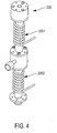
- Each plasma source as shown in figure 2 , here consists of a gas inlet system 25, a discharge chamber in the form of a tube of 201, 202, 203 made of a material inert to plasma and whose diameter is adapted to optimize the transfer of radio frequency power.
- a coupling device 26 for example an antenna
- a tuning box and an RF generator upstream and an isolation discharge capacity downstream, not shown.
- the vacuum in the treatment chamber 10, necessary for the creation of the plasma and for the circulation of the gases, is obtained by pumping using a pump 40.
- the pump 40 is for example a primary or turbomolecular pump connected to the bottom from chamber 10, most often facing sources 201, 202, 203.
- the gas enriched in active species therefore circulates in chamber 10 before being pumped.
- FIG 3 shows a functional perspective view of a configuration of the plasma sources into two independent sub-assemblies 21, 22 in accordance with the treatment method according to the invention.
- the sub-assemblies 21, 22 are arranged in concentric rings. Other configurations are however possible depending on the result that one wishes to obtain in the end.
- Each sub-assembly 21, 22 comprises at least one plasma source making it possible to generate a plasma.
- the figure 3 shows that each subset includes three plasma sources (210, 211 and 212 for the subset 21 and 220, 221 and 222 for the subset 22).
- each source comprises a single discharge chamber (here in the form of a tube), while in the sub-assembly 22, each source 220, 221 and 222 comprises two discharge chambers in series (here in the form of tubes also: tubes 2201 and 2202 as illustrated on the figure 4 ).
- Each plasma source of a subset is supplied by a radiofrequency power Pi and by a gas i of flow n i independent.
- the plasma generated by a sub-assembly (for example the sub-assembly 21) is a gas or a gaseous mixture partially ionized with a chemical nature different from the plasma generated by the other sub-assembly 22.
- a control device controls each of the sub-assemblies 21, 22 according to a specific setting by applying a radio frequency power and a gas flow rate specific to each sub-assembly.
- the plasma processing system therefore makes it possible to control the plasma sources independently of one another by applying a radiofrequency power and / or a different gas flow rate at each subset of sources, in order to be able to control the uniformity of treatment, in particular between the center and the edge of a part to be treated.
- the various plasma sources 210, 211, 212, 220, 221, 222 are advantageously small, with discharge chambers of small dimension, here in the form of tubes of small diameter, which thus allows their multiplication in a subset (in the case of a source comprising a single discharge chamber (here in the form of a tube) or the multiplication of sources (in the case of a source comprising discharge chambers in series).
- the multiplication of sources also makes it possible to increase the number of active species generated by this subset in the treatment chamber. It also makes it possible to optimize and standardize the treatments, even for large diameter plates. Indeed, by the adequate combination of the cones of diffusion of the sources, by using their overlap and / or their superposition, as well as by the management of the circulation of the gas via the pumping of the chamber, it is possible to obtain a uniform treatment surfaces.
- these plasma sources can be placed in different strategic places so as to correspond to the form to be treated, for an optimization of its treatment or of the uniformity of its treatment.
- the method is scalable without limits object size to be treated, particularly for wafer diameters ( "wafers") of 300 mm and 450 mm, adding additional peripheral zones to each other.
- a treatment system here comprising two sub-assemblies arranged in two concentric rings, as illustrated in the figure 3 .
- the central ring 21 here consists of three discharge chambers (here in the form of tubes 210, 211 and 212) constituting the plasma sources (generally between one and six discharge chambers) arranged in the center of the source and supplied by a power radio frequency P1 and by a gas consisting of a mixture of, for example, O 2 , Ar, CF 4 , CHF 3 , NF 3 , H 2 O, H 2 , Cl 2 , CF 3 Br, C x H y F z ..., mixed in a block F1, where F1 implements a mixing operation from a gas 1 of flow 1.1, a gas 2 of flow 2.1, a gas 3 of flow 3.1, etc. up to a gas n of flow n.1.
- a second ring 22 surrounds the central ring, which for example consists of three sources (but preferably between four and eight sources), each consisting of two discharge chambers in series, the ring 22 being concentric with the central ring 21.
- the different discharge chambers (here in the form of tubes) of the ring 22 are supplied by a radiofrequency power P2 and by a gas mixed in a block F2, here a mixture of, for example, gas O 2 , Ar, CF 4 , CHF 3 , NF 3 , H 2 O, H 2 , Cl 2 , CF 3 Br, C x H y F z . .., where the block F2 implements a mixing operation starting from a gas 1 of flow rate 1. 2 , of a gas 2 of flow rate 2.2, of a gas 3 of flow rate 3. 2 , etc. up to a gas n of flow n.2.
- a third ring 23 surrounding the second ring 22 described above comprising from eight to sixteen discharge chambers (here in the form of tubes), the tubes being supplied by a radiofrequency power P3 and supplied by gases mixed in a block F3, which gases are, for example, O 2 , Ar, CF 4 , CHF 3 , NF 3 , H 2 O, H 2 , Cl 2 , CF 3 Br, C x H y F z , etc, where the block F3 implements a mixing operation from a gas 1 of flow 1.3, a gas 2 of flow 2.3, a gas 3 of flow 3.3, etc. up to gas n of flow n.3.
- gases are, for example, O 2 , Ar, CF 4 , CHF 3 , NF 3 , H 2 O, H 2 , Cl 2 , CF 3 Br, C x H y F z , etc, where the block F3 implements a mixing operation from a gas 1 of flow 1.3, a gas 2 of flow 2.3,
- the uniformity of the processes is ensured by the independent control of the different zones of the source in terms of gas flow F1, F2, F3 and radio frequency power P1, P2, P3.
- each ring corresponds to a subset of sources, which subset comprises a gas inlet which is specific to the subset, connected to the gas inlet of each plasma source of the considered subset.
- a control device controls the gas flow in the gas inlet of each sub-assembly. The control device also controls the gas mixture injected into the gas inlet of each sub-assembly.
- each sub-assembly here comprises a conductive element connected to the antenna 26 of each discharge chamber (here in the form of a tube) of the sub-assembly.
- the control device controls the RF power supplied to the conductive element of a sub-assembly.
- the substrate is also put in rotational movement to average the processing speed and thus improve the uniformity.
- concentric rings of anodized aluminum or quartz are typically added between each source and the substrate to be treated, typically in the upper part of the treatment chamber 10, these rings being shower heads (or “ showerheads ”) according to Anglo-Saxon terminology) which are commonly used in semiconductor manufacturing equipment to distribute the injection of chemical species into hundreds of injection points.
- Such rings form small holes drilled in their underside, facing the substrate to be treated. In the present case they make it possible to further improve the uniformity of the treatment or even to reduce the number of discharge chambers necessary for treating a substrate of 300 and 450 mm.
- the parameters of gas flow and radiofrequency power are adjusted on the basis of a performance measurement in terms of uniformity of the process.
- Such an adjustment of the parameters of gas flow and of radiofrequency power is for example carried out in the form of a closed loop or in the form of a loop in advance or " Feed Forward " according to the Anglo-Saxon terminology.
- a “ Feed Forward ” adjustment consists here of measuring the surface condition of the wafer before treatment (such as the thickness of resin for example) in order to adjust the process parameters to compensate for the non-uniformity already present.
- the closed loop here consists in measuring the surface condition of the wafer after treatment in order to adjust the process parameters before treating the next wafer.
- the advantages provided by the plasma processing system described are notably better uniformity and better efficiency in terms of processing speed.
- the multiplexing of the sources allows independent control of the flow of active species in terms of quantity, dissociation rate, chemical composition, and energy in certain work areas, and thus makes it possible to actively correct the treatment of sensitive components.
- the system therefore makes it possible to treat substrates without size limit, which provides a very wide potential for applications, beyond cleaning and removal applications (or “ stripping ” according to Anglo-Saxon terminology).
- the system also allows a uniform distribution of the gas flow of active species. It improves the cleaning efficiency of the residues and the etching speeds, while considerably increasing the selectivity compared to current performance.
- Selectivity is the ratio of the etching speed of the target material (e.g. silicon nitride Si 3 N 4 ) to the etching speed of another exposed material, which ideally should not be etched (e.g. silicon oxide SiO 2 ). Selectivity is critical and must be constantly increased as new technological generations emerge.
- the device with its multiple discharge chambers (here in the form of tubes) makes it possible to increase the selectivity of the plasma processes by independently controlling the etching speed of the target material and that of the other exposed material (s). (s).
- the device provides infinite selectivity.
- the alternating use, or partial recovery, of a withdrawal plasma generated by a sub-assembly and a passivation plasma generated by another sub-assembly makes it possible to substantially improve this selectivity.
- the selectivity is measured by making the ratio, after treatment, of the thickness removed on the material A compared to the thickness removed on the material B for the same duration of treatment. This can also be expressed in the form of the ratio of the etching or shrinking speeds of the two materials.
- Silicon substrates covered with a layer of silicon nitride (Si 3 N 4 ) and silicon substrates covered with a layer of silicon oxide (SiO 2 ) were respectively etched with phosphoric acid .
- Si02 To determine the etching rate of Si02, use an Si substrate covered with Si02 only i.e. Si02 / Si, from which the Si02 is partially removed. To determine the etching speed of Si3N4, use an Si substrate covered with Si3N4 only i.e. Si3N4 / Si or more often an Si substrate with Si3N4 on Si02 i.e. Si3N4 / SiO2 / Si from which the Si3N4 is partially removed.
- the method is applied to the real structure on Si substrate.
- the real structure is most often composite, that is to say made of Si02 zones and Si3N4 / SiO2 zones.
- the geometry and topography of the zones depend on the manufacturing stage (the figure 15 is an example).
- Test plates as above were engraved by the plasma process of the prior art presented by the IMEC R&D center (Belgium) during the PESM 2012 conference in Grenob the.
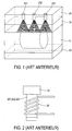
- the plasma etching treatments were carried out in an etching machine from the company LAM RESEARCH as illustrated in the figure 5 : it includes a single discharge chamber and a single chemistry.
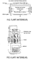
- the applicant carried out selective etching experiments of Si 3 N 4 based on equipment comprising a plasma source composed of several discharge chambers (here in the form of tubes) as illustrated on the figure 6 .
- the discharge tubes are all connected in parallel and controlled with a single generator. It is not possible to independently control the tubes, i.e. to apply different RF power to the different tubes.
- the active gases of type O 2 , N 2 , CF 4 ... are mixed before being injected into the discharge tubes. It is also not possible to inject different gases into the different tubes.
- the plasma source used by the depositor although composed of several discharge tubes, generates a single type of plasma in the treatment chamber, just like traditional plasma sources (microwave or by inductive coupling).
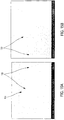
- the comparative examples therefore show that it is not possible to combine a high selectivity with a high etching speed (see the results presented on the figure 8 and comparative example 2).
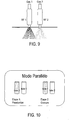
- This process is implemented using a plasma processing device according to the invention comprising two different sets of plasma sources (here represented by the tubes 1 and 2 on the figure 9 ), each tube performing a step (passivation or etching) of the invention (as illustrated in the figure 10 ).
- the operating timing diagrams for each source are shown on the Figures 11A, 11B and 11C , respectively for operation with alternating withdrawal and passivation steps without any overlap, ( figure 11A ), for operation with partially overlapping passivation and removal steps ( figure 11B ) and completely overlapping removal and passivation steps ( figure 11C ).
- the layer of silicon nitride Si 3 N 4 is selectively etched as a mask for the production of so-called STI isolation composite structures ( " Shallow trench Isolation " according to Anglo-Saxon terminology).
- the sequence of passivation and removal steps implementing the conditions 1 of Example 1 is repeated eight times consecutively for a duration of 7 and 15 s respectively.
- the composite structure before removal is illustrated in figure 15A (left), while that after treatment is illustrated in figure 15B (right).
- the silicon nitride Si 3 N 4 is referenced 151 and the silicon oxide 153. There is a suppression of the silicon nitride while the silicon oxide is intact.
Landscapes
- Physics & Mathematics (AREA)
- Engineering & Computer Science (AREA)
- Plasma & Fusion (AREA)
- Chemical & Material Sciences (AREA)
- Analytical Chemistry (AREA)
- Drying Of Semiconductors (AREA)
Applications Claiming Priority (2)
| Application Number | Priority Date | Filing Date | Title |
|---|---|---|---|
| FR1257037A FR2993576B1 (fr) | 2012-07-20 | 2012-07-20 | Dispositif de traitement d'un objet par plasma |
| PCT/FR2013/051768 WO2014013209A1 (fr) | 2012-07-20 | 2013-07-22 | Dispositif de traitement d'un objet par plasma |
Publications (2)
| Publication Number | Publication Date |
|---|---|
| EP2875517A1 EP2875517A1 (fr) | 2015-05-27 |
| EP2875517B1 true EP2875517B1 (fr) | 2020-05-27 |
Family
ID=47227933
Family Applications (1)
| Application Number | Title | Priority Date | Filing Date |
|---|---|---|---|
| EP13756581.8A Active EP2875517B1 (fr) | 2012-07-20 | 2013-07-22 | Dispositif de traitement d'un objet par plasma |
Country Status (9)
Families Citing this family (8)
| Publication number | Priority date | Publication date | Assignee | Title |
|---|---|---|---|---|
| US9378975B2 (en) | 2014-02-10 | 2016-06-28 | Tokyo Electron Limited | Etching method to form spacers having multiple film layers |
| WO2018044713A1 (en) * | 2016-08-29 | 2018-03-08 | Tokyo Electron Limited | Method of quasi-atomic layer etching of silicon nitride |
| JP6836953B2 (ja) * | 2016-12-13 | 2021-03-03 | 東京エレクトロン株式会社 | 窒化シリコンから形成された第1領域を酸化シリコンから形成された第2領域に対して選択的にエッチングする方法 |
| KR102537742B1 (ko) | 2017-02-23 | 2023-05-26 | 도쿄엘렉트론가부시키가이샤 | 자가 정렬 블록 구조물들의 제조를 위한 실리콘 질화물 맨드렐의 이방성 추출 방법 |
| WO2018156975A1 (en) | 2017-02-23 | 2018-08-30 | Tokyo Electron Limited | Method of quasi-atomic layer etching of silicon nitride |
| KR102440367B1 (ko) * | 2017-06-22 | 2022-09-05 | 삼성전자주식회사 | Rps를 이용한 식각 방법 및 그 식각 방법을 포함한 반도체 소자 제조방법 |
| US10658192B2 (en) * | 2017-09-13 | 2020-05-19 | Tokyo Electron Limited | Selective oxide etching method for self-aligned multiple patterning |
| US10607852B2 (en) * | 2017-09-13 | 2020-03-31 | Tokyo Electron Limited | Selective nitride etching method for self-aligned multiple patterning |
Citations (1)
| Publication number | Priority date | Publication date | Assignee | Title |
|---|---|---|---|---|
| JP2007088509A (ja) * | 1996-02-22 | 2007-04-05 | Freescale Semiconductor Inc | 誘導結合プラズマ・リアクタとその方法 |
Family Cites Families (25)
| Publication number | Priority date | Publication date | Assignee | Title |
|---|---|---|---|---|
| US5273609A (en) * | 1990-09-12 | 1993-12-28 | Texas Instruments Incorporated | Method and apparatus for time-division plasma chopping in a multi-channel plasma processing equipment |
| US5296272A (en) * | 1990-10-10 | 1994-03-22 | Hughes Aircraft Company | Method of implanting ions from a plasma into an object |
| JP3752468B2 (ja) * | 1991-04-04 | 2006-03-08 | 株式会社日立製作所 | 半導体装置の製造方法 |
| US6267074B1 (en) * | 1997-02-24 | 2001-07-31 | Foi Corporation | Plasma treatment systems |
| EP1055249A1 (en) * | 1998-02-09 | 2000-11-29 | Applied Materials, Inc. | Plasma assisted processing chamber with separate control of species density |
| US6051073A (en) * | 1998-02-11 | 2000-04-18 | Silicon Genesis Corporation | Perforated shield for plasma immersion ion implantation |
| US20010002584A1 (en) * | 1998-12-01 | 2001-06-07 | Wei Liu | Enhanced plasma mode and system for plasma immersion ion implantation |
| US20060124588A1 (en) * | 1999-01-05 | 2006-06-15 | Berg & Berg Enterprises, Llc | System and method for reducing metal oxides with hydrogen radicals |
| JP2002100623A (ja) * | 2000-09-20 | 2002-04-05 | Fuji Daiichi Seisakusho:Kk | 薄膜半導体製造装置 |
| JP2004265627A (ja) * | 2003-02-14 | 2004-09-24 | Masato Toshima | プラズマ発生装置およびプラズマエッチング装置 |
| US20060276043A1 (en) * | 2003-03-21 | 2006-12-07 | Johnson Mark A L | Method and systems for single- or multi-period edge definition lithography |
| AT412719B (de) * | 2003-06-16 | 2005-06-27 | Eckelt Glas Gmbh | Verfahren und vorrichtung zum bereichsweisen entschichten von glasscheiben |
| US7015415B2 (en) * | 2004-02-18 | 2006-03-21 | Dry Plasma Systems, Inc. | Higher power density downstream plasma |
| TWI349042B (en) * | 2006-02-09 | 2011-09-21 | Sputtering system providing large area sputtering and plasma-assisted reactive gas dissociation | |
| KR100799175B1 (ko) * | 2006-04-21 | 2008-02-01 | 주식회사 뉴파워 프라즈마 | 플라즈마 프로세싱 시스템 및 그 제어 방법 |
| EP1936656A1 (en) * | 2006-12-21 | 2008-06-25 | Nederlandse Organisatie voor Toegepast-Natuuurwetenschappelijk Onderzoek TNO | Plasma generator and method for cleaning an object |
| US7976674B2 (en) * | 2007-06-13 | 2011-07-12 | Tokyo Electron Limited | Embedded multi-inductive large area plasma source |
| CN201228282Y (zh) * | 2007-12-24 | 2009-04-29 | 杨思泽 | 脉冲高能量密度等离子体辅助多源复合材料表面改性装置 |
| JP5214261B2 (ja) * | 2008-01-25 | 2013-06-19 | ルネサスエレクトロニクス株式会社 | 半導体装置の製造方法 |
| US20090286397A1 (en) * | 2008-05-15 | 2009-11-19 | Lam Research Corporation | Selective inductive double patterning |
| US8207470B2 (en) * | 2008-10-20 | 2012-06-26 | Industry-University Cooperation Foundation Hanyang University | Apparatus for generating remote plasma |
| JP2010161350A (ja) * | 2008-12-09 | 2010-07-22 | Hitachi Kokusai Electric Inc | 基板処理方法 |
| CN102110650A (zh) * | 2009-12-29 | 2011-06-29 | 中国科学院微电子研究所 | 一种半导体器件及其制造方法 |
| US8574447B2 (en) * | 2010-03-31 | 2013-11-05 | Lam Research Corporation | Inorganic rapid alternating process for silicon etch |
| US9155181B2 (en) * | 2010-08-06 | 2015-10-06 | Lam Research Corporation | Distributed multi-zone plasma source systems, methods and apparatus |
-
2012
- 2012-07-20 FR FR1257037A patent/FR2993576B1/fr active Active
-
2013
- 2013-07-22 SG SG11201500389UA patent/SG11201500389UA/en unknown
- 2013-07-22 KR KR1020157004383A patent/KR102060671B1/ko active Active
- 2013-07-22 JP JP2015522156A patent/JP6298814B2/ja active Active
- 2013-07-22 WO PCT/FR2013/051768 patent/WO2014013209A1/fr active Application Filing
- 2013-07-22 TW TW102126199A patent/TWI601181B/zh active
- 2013-07-22 EP EP13756581.8A patent/EP2875517B1/fr active Active
- 2013-07-22 US US14/415,976 patent/US20150243485A1/en not_active Abandoned
- 2013-07-22 CN CN201380038733.8A patent/CN104685605B/zh active Active
-
2018
- 2018-01-13 US US15/870,890 patent/US11075057B2/en active Active
Patent Citations (1)
| Publication number | Priority date | Publication date | Assignee | Title |
|---|---|---|---|---|
| JP2007088509A (ja) * | 1996-02-22 | 2007-04-05 | Freescale Semiconductor Inc | 誘導結合プラズマ・リアクタとその方法 |
Also Published As
| Publication number | Publication date |
|---|---|
| TWI601181B (zh) | 2017-10-01 |
| CN104685605A (zh) | 2015-06-03 |
| JP2015526897A (ja) | 2015-09-10 |
| US11075057B2 (en) | 2021-07-27 |
| US20150243485A1 (en) | 2015-08-27 |
| FR2993576B1 (fr) | 2018-05-18 |
| FR2993576A1 (fr) | 2014-01-24 |
| EP2875517A1 (fr) | 2015-05-27 |
| TW201415520A (zh) | 2014-04-16 |
| WO2014013209A1 (fr) | 2014-01-23 |
| JP6298814B2 (ja) | 2018-03-20 |
| US20180158651A1 (en) | 2018-06-07 |
| KR20150038172A (ko) | 2015-04-08 |
| SG11201500389UA (en) | 2015-03-30 |
| CN104685605B (zh) | 2017-05-17 |
| KR102060671B1 (ko) | 2019-12-30 |
Similar Documents
| Publication | Publication Date | Title |
|---|---|---|
| EP2875517B1 (fr) | Dispositif de traitement d'un objet par plasma | |
| JP6882469B2 (ja) | 高アスペクト比の構造体のための除去方法 | |
| US10566206B2 (en) | Systems and methods for anisotropic material breakthrough | |
| JP5038151B2 (ja) | 基板最適化のためのプラズマ処理ステップ交互実行方法及び装置 | |
| EP2939262B1 (fr) | Procédé microélectronique de gravure d'une couche | |
| US9190290B2 (en) | Halogen-free gas-phase silicon etch | |
| US20140342569A1 (en) | Near surface etch selectivity enhancement | |
| FR3017241A1 (fr) | Procede de gravure plasma | |
| FR2492591A1 (fr) | Procede de fabrication d'un circuit integre | |
| US20210111033A1 (en) | Isotropic silicon nitride removal | |
| US10283324B1 (en) | Oxygen treatment for nitride etching | |
| US20240290623A1 (en) | Processing methods to improve etched silicon-and-germanium-containing material surface roughness | |
| CN114068320A (zh) | 硅的干蚀刻方法 | |
| KR102469451B1 (ko) | 마이크로전자 공작물의 제조를 위해 실리콘 질화물층을 영역 선택 에칭하는 방법 | |
| US11328909B2 (en) | Chamber conditioning and removal processes | |
| US10886137B2 (en) | Selective nitride removal | |
| US10128086B1 (en) | Silicon pretreatment for nitride removal | |
| US20250022714A1 (en) | Cyclic etch of silicon oxide and silicon nitride | |
| CN120033146B (zh) | 高深宽比刻蚀结构形貌改善方法、刻蚀设备及半导体结构 | |
| JP6259610B2 (ja) | プラズマ処理装置およびプラズマ処理方法 | |
| WO2014001709A1 (fr) | Équipement de traitement de surface par plasma généré ex-situ et procédé associé | |
| FR2805185A1 (fr) | Procede de nettoyage a passivation exempt d'oxygene dans un reacteur plasma a couplage inductif |
Legal Events
| Date | Code | Title | Description |
|---|---|---|---|
| PUAI | Public reference made under article 153(3) epc to a published international application that has entered the european phase |
Free format text: ORIGINAL CODE: 0009012 |
|
| 17P | Request for examination filed |
Effective date: 20141231 |
|
| AK | Designated contracting states |
Kind code of ref document: A1 Designated state(s): AL AT BE BG CH CY CZ DE DK EE ES FI FR GB GR HR HU IE IS IT LI LT LU LV MC MK MT NL NO PL PT RO RS SE SI SK SM TR |
|
| AX | Request for extension of the european patent |
Extension state: BA ME |
|
| DAX | Request for extension of the european patent (deleted) | ||
| STAA | Information on the status of an ep patent application or granted ep patent |
Free format text: STATUS: EXAMINATION IS IN PROGRESS |
|
| 17Q | First examination report despatched |
Effective date: 20170309 |
|
| 19U | Interruption of proceedings before grant |
Effective date: 20150527 |
|
| 19W | Proceedings resumed before grant after interruption of proceedings |
Effective date: 20191202 |
|
| RAP1 | Party data changed (applicant data changed or rights of an application transferred) |
Owner name: PLASMA-THERM, LLC |
|
| GRAP | Despatch of communication of intention to grant a patent |
Free format text: ORIGINAL CODE: EPIDOSNIGR1 |
|
| STAA | Information on the status of an ep patent application or granted ep patent |
Free format text: STATUS: GRANT OF PATENT IS INTENDED |
|
| INTG | Intention to grant announced |
Effective date: 20200310 |
|
| GRAS | Grant fee paid |
Free format text: ORIGINAL CODE: EPIDOSNIGR3 |
|
| GRAA | (expected) grant |
Free format text: ORIGINAL CODE: 0009210 |
|
| STAA | Information on the status of an ep patent application or granted ep patent |
Free format text: STATUS: THE PATENT HAS BEEN GRANTED |
|
| AK | Designated contracting states |
Kind code of ref document: B1 Designated state(s): AL AT BE BG CH CY CZ DE DK EE ES FI FR GB GR HR HU IE IS IT LI LT LU LV MC MK MT NL NO PL PT RO RS SE SI SK SM TR |
|
| REG | Reference to a national code |
Ref country code: GB Ref legal event code: FG4D Free format text: NOT ENGLISH |
|
| REG | Reference to a national code |
Ref country code: CH Ref legal event code: EP |
|
| REG | Reference to a national code |
Ref country code: AT Ref legal event code: REF Ref document number: 1275440 Country of ref document: AT Kind code of ref document: T Effective date: 20200615 |
|
| REG | Reference to a national code |
Ref country code: DE Ref legal event code: R096 Ref document number: 602013069414 Country of ref document: DE |
|
| REG | Reference to a national code |
Ref country code: CH Ref legal event code: NV Representative=s name: NOVAGRAAF INTERNATIONAL SA, CH |
|
| REG | Reference to a national code |
Ref country code: LT Ref legal event code: MG4D |
|
| PG25 | Lapsed in a contracting state [announced via postgrant information from national office to epo] |
Ref country code: SE Free format text: LAPSE BECAUSE OF FAILURE TO SUBMIT A TRANSLATION OF THE DESCRIPTION OR TO PAY THE FEE WITHIN THE PRESCRIBED TIME-LIMIT Effective date: 20200527 Ref country code: LT Free format text: LAPSE BECAUSE OF FAILURE TO SUBMIT A TRANSLATION OF THE DESCRIPTION OR TO PAY THE FEE WITHIN THE PRESCRIBED TIME-LIMIT Effective date: 20200527 Ref country code: PT Free format text: LAPSE BECAUSE OF FAILURE TO SUBMIT A TRANSLATION OF THE DESCRIPTION OR TO PAY THE FEE WITHIN THE PRESCRIBED TIME-LIMIT Effective date: 20200928 Ref country code: IS Free format text: LAPSE BECAUSE OF FAILURE TO SUBMIT A TRANSLATION OF THE DESCRIPTION OR TO PAY THE FEE WITHIN THE PRESCRIBED TIME-LIMIT Effective date: 20200927 Ref country code: FI Free format text: LAPSE BECAUSE OF FAILURE TO SUBMIT A TRANSLATION OF THE DESCRIPTION OR TO PAY THE FEE WITHIN THE PRESCRIBED TIME-LIMIT Effective date: 20200527 Ref country code: NO Free format text: LAPSE BECAUSE OF FAILURE TO SUBMIT A TRANSLATION OF THE DESCRIPTION OR TO PAY THE FEE WITHIN THE PRESCRIBED TIME-LIMIT Effective date: 20200827 Ref country code: GR Free format text: LAPSE BECAUSE OF FAILURE TO SUBMIT A TRANSLATION OF THE DESCRIPTION OR TO PAY THE FEE WITHIN THE PRESCRIBED TIME-LIMIT Effective date: 20200828 |
|
| REG | Reference to a national code |
Ref country code: NL Ref legal event code: MP Effective date: 20200527 |
|
| PG25 | Lapsed in a contracting state [announced via postgrant information from national office to epo] |
Ref country code: RS Free format text: LAPSE BECAUSE OF FAILURE TO SUBMIT A TRANSLATION OF THE DESCRIPTION OR TO PAY THE FEE WITHIN THE PRESCRIBED TIME-LIMIT Effective date: 20200527 Ref country code: BG Free format text: LAPSE BECAUSE OF FAILURE TO SUBMIT A TRANSLATION OF THE DESCRIPTION OR TO PAY THE FEE WITHIN THE PRESCRIBED TIME-LIMIT Effective date: 20200827 Ref country code: HR Free format text: LAPSE BECAUSE OF FAILURE TO SUBMIT A TRANSLATION OF THE DESCRIPTION OR TO PAY THE FEE WITHIN THE PRESCRIBED TIME-LIMIT Effective date: 20200527 Ref country code: LV Free format text: LAPSE BECAUSE OF FAILURE TO SUBMIT A TRANSLATION OF THE DESCRIPTION OR TO PAY THE FEE WITHIN THE PRESCRIBED TIME-LIMIT Effective date: 20200527 |
|
| REG | Reference to a national code |
Ref country code: AT Ref legal event code: MK05 Ref document number: 1275440 Country of ref document: AT Kind code of ref document: T Effective date: 20200527 |
|
| PG25 | Lapsed in a contracting state [announced via postgrant information from national office to epo] |
Ref country code: NL Free format text: LAPSE BECAUSE OF FAILURE TO SUBMIT A TRANSLATION OF THE DESCRIPTION OR TO PAY THE FEE WITHIN THE PRESCRIBED TIME-LIMIT Effective date: 20200527 Ref country code: AL Free format text: LAPSE BECAUSE OF FAILURE TO SUBMIT A TRANSLATION OF THE DESCRIPTION OR TO PAY THE FEE WITHIN THE PRESCRIBED TIME-LIMIT Effective date: 20200527 |
|
| PG25 | Lapsed in a contracting state [announced via postgrant information from national office to epo] |
Ref country code: RO Free format text: LAPSE BECAUSE OF FAILURE TO SUBMIT A TRANSLATION OF THE DESCRIPTION OR TO PAY THE FEE WITHIN THE PRESCRIBED TIME-LIMIT Effective date: 20200527 Ref country code: IT Free format text: LAPSE BECAUSE OF FAILURE TO SUBMIT A TRANSLATION OF THE DESCRIPTION OR TO PAY THE FEE WITHIN THE PRESCRIBED TIME-LIMIT Effective date: 20200527 Ref country code: CZ Free format text: LAPSE BECAUSE OF FAILURE TO SUBMIT A TRANSLATION OF THE DESCRIPTION OR TO PAY THE FEE WITHIN THE PRESCRIBED TIME-LIMIT Effective date: 20200527 Ref country code: SM Free format text: LAPSE BECAUSE OF FAILURE TO SUBMIT A TRANSLATION OF THE DESCRIPTION OR TO PAY THE FEE WITHIN THE PRESCRIBED TIME-LIMIT Effective date: 20200527 Ref country code: EE Free format text: LAPSE BECAUSE OF FAILURE TO SUBMIT A TRANSLATION OF THE DESCRIPTION OR TO PAY THE FEE WITHIN THE PRESCRIBED TIME-LIMIT Effective date: 20200527 Ref country code: AT Free format text: LAPSE BECAUSE OF FAILURE TO SUBMIT A TRANSLATION OF THE DESCRIPTION OR TO PAY THE FEE WITHIN THE PRESCRIBED TIME-LIMIT Effective date: 20200527 Ref country code: ES Free format text: LAPSE BECAUSE OF FAILURE TO SUBMIT A TRANSLATION OF THE DESCRIPTION OR TO PAY THE FEE WITHIN THE PRESCRIBED TIME-LIMIT Effective date: 20200527 Ref country code: DK Free format text: LAPSE BECAUSE OF FAILURE TO SUBMIT A TRANSLATION OF THE DESCRIPTION OR TO PAY THE FEE WITHIN THE PRESCRIBED TIME-LIMIT Effective date: 20200527 |
|
| PG25 | Lapsed in a contracting state [announced via postgrant information from national office to epo] |
Ref country code: SK Free format text: LAPSE BECAUSE OF FAILURE TO SUBMIT A TRANSLATION OF THE DESCRIPTION OR TO PAY THE FEE WITHIN THE PRESCRIBED TIME-LIMIT Effective date: 20200527 Ref country code: MC Free format text: LAPSE BECAUSE OF FAILURE TO SUBMIT A TRANSLATION OF THE DESCRIPTION OR TO PAY THE FEE WITHIN THE PRESCRIBED TIME-LIMIT Effective date: 20200527 Ref country code: PL Free format text: LAPSE BECAUSE OF FAILURE TO SUBMIT A TRANSLATION OF THE DESCRIPTION OR TO PAY THE FEE WITHIN THE PRESCRIBED TIME-LIMIT Effective date: 20200527 |
|
| REG | Reference to a national code |
Ref country code: DE Ref legal event code: R097 Ref document number: 602013069414 Country of ref document: DE |
|
| PLBE | No opposition filed within time limit |
Free format text: ORIGINAL CODE: 0009261 |
|
| STAA | Information on the status of an ep patent application or granted ep patent |
Free format text: STATUS: NO OPPOSITION FILED WITHIN TIME LIMIT |
|
| REG | Reference to a national code |
Ref country code: BE Ref legal event code: MM Effective date: 20200731 |
|
| PG25 | Lapsed in a contracting state [announced via postgrant information from national office to epo] |
Ref country code: LU Free format text: LAPSE BECAUSE OF NON-PAYMENT OF DUE FEES Effective date: 20200722 |
|
| 26N | No opposition filed |
Effective date: 20210302 |
|
| PG25 | Lapsed in a contracting state [announced via postgrant information from national office to epo] |
Ref country code: SI Free format text: LAPSE BECAUSE OF FAILURE TO SUBMIT A TRANSLATION OF THE DESCRIPTION OR TO PAY THE FEE WITHIN THE PRESCRIBED TIME-LIMIT Effective date: 20200527 Ref country code: BE Free format text: LAPSE BECAUSE OF NON-PAYMENT OF DUE FEES Effective date: 20200731 |
|
| PG25 | Lapsed in a contracting state [announced via postgrant information from national office to epo] |
Ref country code: IE Free format text: LAPSE BECAUSE OF NON-PAYMENT OF DUE FEES Effective date: 20200722 |
|
| PG25 | Lapsed in a contracting state [announced via postgrant information from national office to epo] |
Ref country code: TR Free format text: LAPSE BECAUSE OF FAILURE TO SUBMIT A TRANSLATION OF THE DESCRIPTION OR TO PAY THE FEE WITHIN THE PRESCRIBED TIME-LIMIT Effective date: 20200527 Ref country code: MT Free format text: LAPSE BECAUSE OF FAILURE TO SUBMIT A TRANSLATION OF THE DESCRIPTION OR TO PAY THE FEE WITHIN THE PRESCRIBED TIME-LIMIT Effective date: 20200527 Ref country code: CY Free format text: LAPSE BECAUSE OF FAILURE TO SUBMIT A TRANSLATION OF THE DESCRIPTION OR TO PAY THE FEE WITHIN THE PRESCRIBED TIME-LIMIT Effective date: 20200527 |
|
| PG25 | Lapsed in a contracting state [announced via postgrant information from national office to epo] |
Ref country code: MK Free format text: LAPSE BECAUSE OF FAILURE TO SUBMIT A TRANSLATION OF THE DESCRIPTION OR TO PAY THE FEE WITHIN THE PRESCRIBED TIME-LIMIT Effective date: 20200527 |
|
| P01 | Opt-out of the competence of the unified patent court (upc) registered |
Effective date: 20230524 |
|
| PGFP | Annual fee paid to national office [announced via postgrant information from national office to epo] |
Ref country code: DE Payment date: 20240719 Year of fee payment: 12 |
|
| PGFP | Annual fee paid to national office [announced via postgrant information from national office to epo] |
Ref country code: GB Payment date: 20240725 Year of fee payment: 12 |
|
| PGFP | Annual fee paid to national office [announced via postgrant information from national office to epo] |
Ref country code: FR Payment date: 20240730 Year of fee payment: 12 |
|
| PGFP | Annual fee paid to national office [announced via postgrant information from national office to epo] |
Ref country code: CH Payment date: 20240801 Year of fee payment: 12 |