JP6836953B2 - 窒化シリコンから形成された第1領域を酸化シリコンから形成された第2領域に対して選択的にエッチングする方法 - Google Patents
窒化シリコンから形成された第1領域を酸化シリコンから形成された第2領域に対して選択的にエッチングする方法 Download PDFInfo
- Publication number
- JP6836953B2 JP6836953B2 JP2017086521A JP2017086521A JP6836953B2 JP 6836953 B2 JP6836953 B2 JP 6836953B2 JP 2017086521 A JP2017086521 A JP 2017086521A JP 2017086521 A JP2017086521 A JP 2017086521A JP 6836953 B2 JP6836953 B2 JP 6836953B2
- Authority
- JP
- Japan
- Prior art keywords
- gas
- region
- plasma
- chamber
- film
- Prior art date
- Legal status (The legal status is an assumption and is not a legal conclusion. Google has not performed a legal analysis and makes no representation as to the accuracy of the status listed.)
- Active
Links
- 238000000034 method Methods 0.000 title claims description 201
- 238000005530 etching Methods 0.000 title claims description 63
- HQVNEWCFYHHQES-UHFFFAOYSA-N silicon nitride Chemical compound N12[Si]34N5[Si]62N3[Si]51N64 HQVNEWCFYHHQES-UHFFFAOYSA-N 0.000 title claims description 39
- 229910052581 Si3N4 Inorganic materials 0.000 title claims description 38
- VYPSYNLAJGMNEJ-UHFFFAOYSA-N Silicium dioxide Chemical compound O=[Si]=O VYPSYNLAJGMNEJ-UHFFFAOYSA-N 0.000 title claims description 35
- 229910052814 silicon oxide Inorganic materials 0.000 title claims description 32
- 239000007789 gas Substances 0.000 claims description 379
- 230000008569 process Effects 0.000 claims description 56
- 239000001301 oxygen Substances 0.000 claims description 47
- 229910052760 oxygen Inorganic materials 0.000 claims description 47
- 238000012545 processing Methods 0.000 claims description 47
- QVGXLLKOCUKJST-UHFFFAOYSA-N atomic oxygen Chemical compound [O] QVGXLLKOCUKJST-UHFFFAOYSA-N 0.000 claims description 46
- 239000001257 hydrogen Substances 0.000 claims description 46
- 229910052739 hydrogen Inorganic materials 0.000 claims description 46
- UFHFLCQGNIYNRP-UHFFFAOYSA-N Hydrogen Chemical compound [H][H] UFHFLCQGNIYNRP-UHFFFAOYSA-N 0.000 claims description 41
- 229910052731 fluorine Inorganic materials 0.000 claims description 36
- 239000011737 fluorine Substances 0.000 claims description 36
- YCKRFDGAMUMZLT-UHFFFAOYSA-N Fluorine atom Chemical compound [F] YCKRFDGAMUMZLT-UHFFFAOYSA-N 0.000 claims description 34
- 229910052710 silicon Inorganic materials 0.000 claims description 33
- 239000010703 silicon Substances 0.000 claims description 32
- 150000002500 ions Chemical class 0.000 claims description 7
- 230000015572 biosynthetic process Effects 0.000 claims description 6
- 230000001590 oxidative effect Effects 0.000 claims description 2
- XUIMIQQOPSSXEZ-UHFFFAOYSA-N Silicon Chemical compound [Si] XUIMIQQOPSSXEZ-UHFFFAOYSA-N 0.000 description 31
- 238000002474 experimental method Methods 0.000 description 31
- 238000010586 diagram Methods 0.000 description 22
- 238000010926 purge Methods 0.000 description 13
- FZHAPNGMFPVSLP-UHFFFAOYSA-N silanamine Chemical compound [SiH3]N FZHAPNGMFPVSLP-UHFFFAOYSA-N 0.000 description 10
- 230000004048 modification Effects 0.000 description 8
- 238000012986 modification Methods 0.000 description 8
- 239000000463 material Substances 0.000 description 7
- 239000002243 precursor Substances 0.000 description 7
- 230000003647 oxidation Effects 0.000 description 6
- 238000007254 oxidation reaction Methods 0.000 description 6
- 229910052782 aluminium Inorganic materials 0.000 description 5
- XAGFODPZIPBFFR-UHFFFAOYSA-N aluminium Chemical compound [Al] XAGFODPZIPBFFR-UHFFFAOYSA-N 0.000 description 5
- NBVXSUQYWXRMNV-UHFFFAOYSA-N fluoromethane Chemical compound FC NBVXSUQYWXRMNV-UHFFFAOYSA-N 0.000 description 5
- -1 for example Chemical class 0.000 description 5
- 238000004519 manufacturing process Methods 0.000 description 5
- 238000001020 plasma etching Methods 0.000 description 5
- 238000009832 plasma treatment Methods 0.000 description 5
- 230000000052 comparative effect Effects 0.000 description 4
- 230000005669 field effect Effects 0.000 description 4
- 125000004435 hydrogen atom Chemical group [H]* 0.000 description 4
- MYMOFIZGZYHOMD-UHFFFAOYSA-N Dioxygen Chemical compound O=O MYMOFIZGZYHOMD-UHFFFAOYSA-N 0.000 description 3
- 229910003902 SiCl 4 Inorganic materials 0.000 description 3
- 125000004429 atom Chemical group 0.000 description 3
- 239000002131 composite material Substances 0.000 description 3
- 229910001882 dioxygen Inorganic materials 0.000 description 3
- 150000002431 hydrogen Chemical class 0.000 description 3
- 239000010453 quartz Substances 0.000 description 3
- 230000009467 reduction Effects 0.000 description 3
- 238000002407 reforming Methods 0.000 description 3
- IJGRMHOSHXDMSA-UHFFFAOYSA-N Atomic nitrogen Chemical compound N#N IJGRMHOSHXDMSA-UHFFFAOYSA-N 0.000 description 2
- 125000003277 amino group Chemical group 0.000 description 2
- 238000000231 atomic layer deposition Methods 0.000 description 2
- 239000000919 ceramic Substances 0.000 description 2
- 238000006243 chemical reaction Methods 0.000 description 2
- 125000001309 chloro group Chemical group Cl* 0.000 description 2
- 239000011248 coating agent Substances 0.000 description 2
- 238000000576 coating method Methods 0.000 description 2
- 229910001873 dinitrogen Inorganic materials 0.000 description 2
- 125000001153 fluoro group Chemical group F* 0.000 description 2
- 238000009616 inductively coupled plasma Methods 0.000 description 2
- 239000011261 inert gas Substances 0.000 description 2
- 239000012528 membrane Substances 0.000 description 2
- 229910052751 metal Inorganic materials 0.000 description 2
- 239000002184 metal Substances 0.000 description 2
- 125000004430 oxygen atom Chemical group O* 0.000 description 2
- 230000002093 peripheral effect Effects 0.000 description 2
- 238000004062 sedimentation Methods 0.000 description 2
- 238000004544 sputter deposition Methods 0.000 description 2
- 238000003860 storage Methods 0.000 description 2
- 238000012546 transfer Methods 0.000 description 2
- RYGMFSIKBFXOCR-UHFFFAOYSA-N Copper Chemical compound [Cu] RYGMFSIKBFXOCR-UHFFFAOYSA-N 0.000 description 1
- 101001139126 Homo sapiens Krueppel-like factor 6 Proteins 0.000 description 1
- 101150087840 UL11 gene Proteins 0.000 description 1
- 239000006227 byproduct Substances 0.000 description 1
- 229910052801 chlorine Inorganic materials 0.000 description 1
- 239000004020 conductor Substances 0.000 description 1
- 229910052802 copper Inorganic materials 0.000 description 1
- 239000010949 copper Substances 0.000 description 1
- 230000008878 coupling Effects 0.000 description 1
- 238000010168 coupling process Methods 0.000 description 1
- 238000005859 coupling reaction Methods 0.000 description 1
- 239000003989 dielectric material Substances 0.000 description 1
- 238000010438 heat treatment Methods 0.000 description 1
- 230000006698 induction Effects 0.000 description 1
- 239000011810 insulating material Substances 0.000 description 1
- 239000013067 intermediate product Substances 0.000 description 1
- 230000007246 mechanism Effects 0.000 description 1
- 230000000149 penetrating effect Effects 0.000 description 1
- 229910021420 polycrystalline silicon Inorganic materials 0.000 description 1
- 239000000047 product Substances 0.000 description 1
- 239000003507 refrigerant Substances 0.000 description 1
- 239000013049 sediment Substances 0.000 description 1
- 239000004065 semiconductor Substances 0.000 description 1
- 238000000992 sputter etching Methods 0.000 description 1
- 229910001220 stainless steel Inorganic materials 0.000 description 1
- 239000010935 stainless steel Substances 0.000 description 1
- XLYOFNOQVPJJNP-UHFFFAOYSA-N water Substances O XLYOFNOQVPJJNP-UHFFFAOYSA-N 0.000 description 1
Images


Classifications
-
- H—ELECTRICITY
- H01—ELECTRIC ELEMENTS
- H01J—ELECTRIC DISCHARGE TUBES OR DISCHARGE LAMPS
- H01J37/00—Discharge tubes with provision for introducing objects or material to be exposed to the discharge, e.g. for the purpose of examination or processing thereof
- H01J37/32—Gas-filled discharge tubes
- H01J37/32009—Arrangements for generation of plasma specially adapted for examination or treatment of objects, e.g. plasma sources
- H01J37/32082—Radio frequency generated discharge
- H01J37/321—Radio frequency generated discharge the radio frequency energy being inductively coupled to the plasma
- H01J37/3211—Antennas, e.g. particular shapes of coils
-
- H—ELECTRICITY
- H01—ELECTRIC ELEMENTS
- H01J—ELECTRIC DISCHARGE TUBES OR DISCHARGE LAMPS
- H01J37/00—Discharge tubes with provision for introducing objects or material to be exposed to the discharge, e.g. for the purpose of examination or processing thereof
- H01J37/32—Gas-filled discharge tubes
- H01J37/32009—Arrangements for generation of plasma specially adapted for examination or treatment of objects, e.g. plasma sources
- H01J37/32082—Radio frequency generated discharge
- H01J37/32137—Radio frequency generated discharge controlling of the discharge by modulation of energy
-
- H—ELECTRICITY
- H01—ELECTRIC ELEMENTS
- H01J—ELECTRIC DISCHARGE TUBES OR DISCHARGE LAMPS
- H01J37/00—Discharge tubes with provision for introducing objects or material to be exposed to the discharge, e.g. for the purpose of examination or processing thereof
- H01J37/32—Gas-filled discharge tubes
- H01J37/32009—Arrangements for generation of plasma specially adapted for examination or treatment of objects, e.g. plasma sources
- H01J37/32082—Radio frequency generated discharge
- H01J37/32174—Circuits specially adapted for controlling the RF discharge
-
- H—ELECTRICITY
- H01—ELECTRIC ELEMENTS
- H01J—ELECTRIC DISCHARGE TUBES OR DISCHARGE LAMPS
- H01J37/00—Discharge tubes with provision for introducing objects or material to be exposed to the discharge, e.g. for the purpose of examination or processing thereof
- H01J37/32—Gas-filled discharge tubes
- H01J37/32431—Constructional details of the reactor
- H01J37/3244—Gas supply means
- H01J37/32449—Gas control, e.g. control of the gas flow
-
- H—ELECTRICITY
- H01—ELECTRIC ELEMENTS
- H01L—SEMICONDUCTOR DEVICES NOT COVERED BY CLASS H10
- H01L21/00—Processes or apparatus adapted for the manufacture or treatment of semiconductor or solid state devices or of parts thereof
- H01L21/02—Manufacture or treatment of semiconductor devices or of parts thereof
- H01L21/04—Manufacture or treatment of semiconductor devices or of parts thereof the devices having at least one potential-jump barrier or surface barrier, e.g. PN junction, depletion layer or carrier concentration layer
- H01L21/18—Manufacture or treatment of semiconductor devices or of parts thereof the devices having at least one potential-jump barrier or surface barrier, e.g. PN junction, depletion layer or carrier concentration layer the devices having semiconductor bodies comprising elements of Group IV of the Periodic System or AIIIBV compounds with or without impurities, e.g. doping materials
- H01L21/30—Treatment of semiconductor bodies using processes or apparatus not provided for in groups H01L21/20 - H01L21/26
- H01L21/302—Treatment of semiconductor bodies using processes or apparatus not provided for in groups H01L21/20 - H01L21/26 to change their surface-physical characteristics or shape, e.g. etching, polishing, cutting
- H01L21/306—Chemical or electrical treatment, e.g. electrolytic etching
- H01L21/3065—Plasma etching; Reactive-ion etching
-
- H—ELECTRICITY
- H01—ELECTRIC ELEMENTS
- H01L—SEMICONDUCTOR DEVICES NOT COVERED BY CLASS H10
- H01L21/00—Processes or apparatus adapted for the manufacture or treatment of semiconductor or solid state devices or of parts thereof
- H01L21/02—Manufacture or treatment of semiconductor devices or of parts thereof
- H01L21/04—Manufacture or treatment of semiconductor devices or of parts thereof the devices having at least one potential-jump barrier or surface barrier, e.g. PN junction, depletion layer or carrier concentration layer
- H01L21/18—Manufacture or treatment of semiconductor devices or of parts thereof the devices having at least one potential-jump barrier or surface barrier, e.g. PN junction, depletion layer or carrier concentration layer the devices having semiconductor bodies comprising elements of Group IV of the Periodic System or AIIIBV compounds with or without impurities, e.g. doping materials
- H01L21/30—Treatment of semiconductor bodies using processes or apparatus not provided for in groups H01L21/20 - H01L21/26
- H01L21/31—Treatment of semiconductor bodies using processes or apparatus not provided for in groups H01L21/20 - H01L21/26 to form insulating layers thereon, e.g. for masking or by using photolithographic techniques; After treatment of these layers; Selection of materials for these layers
- H01L21/3105—After-treatment
- H01L21/311—Etching the insulating layers by chemical or physical means
- H01L21/31105—Etching inorganic layers
- H01L21/31111—Etching inorganic layers by chemical means
- H01L21/31116—Etching inorganic layers by chemical means by dry-etching
-
- H—ELECTRICITY
- H01—ELECTRIC ELEMENTS
- H01L—SEMICONDUCTOR DEVICES NOT COVERED BY CLASS H10
- H01L21/00—Processes or apparatus adapted for the manufacture or treatment of semiconductor or solid state devices or of parts thereof
- H01L21/67—Apparatus specially adapted for handling semiconductor or electric solid state devices during manufacture or treatment thereof; Apparatus specially adapted for handling wafers during manufacture or treatment of semiconductor or electric solid state devices or components ; Apparatus not specifically provided for elsewhere
- H01L21/67005—Apparatus not specifically provided for elsewhere
- H01L21/67011—Apparatus for manufacture or treatment
- H01L21/67017—Apparatus for fluid treatment
- H01L21/67063—Apparatus for fluid treatment for etching
- H01L21/67069—Apparatus for fluid treatment for etching for drying etching
-
- H—ELECTRICITY
- H01—ELECTRIC ELEMENTS
- H01J—ELECTRIC DISCHARGE TUBES OR DISCHARGE LAMPS
- H01J2237/00—Discharge tubes exposing object to beam, e.g. for analysis treatment, etching, imaging
- H01J2237/32—Processing objects by plasma generation
- H01J2237/33—Processing objects by plasma generation characterised by the type of processing
- H01J2237/334—Etching
- H01J2237/3341—Reactive etching
Description
・チャンバ12cの圧力:400[mTorr](53.33[Pa])
・高周波電源70A及び70Bの高周波:27[MHz]、600[W]
・バイアス用の高周波:0[W]
・NF3ガスの流量:45[sccm]
・O2ガスの流量:300[sccm]
・Arガスの流量:100[sccm]
・処理時間:10[秒]
・チャンバ12cの圧力:30[mTorr](4[Pa])
・高周波電源70A及び70Bの高周波:0[W]
・バイアス用の高周波:13.56[MHz]、50[W]
・H2ガスの流量:100[sccm]
・処理時間:15[秒]
<第2の実験における工程ST2のパラメータ>
・チャンバ12cの圧力:400[mTorr](53.33[Pa])
・高周波電源70A及び70Bの高周波:27[MHz]、600[W]
・バイアス用の高周波:0[W]
・NF3ガスの流量:45[sccm]
・H2ガスの流量:60[sccm]
・O2ガスの流量:300[sccm]
・Arガスの流量:100[sccm]
・処理時間:10[秒]
・チャンバ12cの圧力:30[mTorr](4[Pa])
・高周波電源70A及び70Bの高周波:0[W]
・バイアス用の高周波:13.56[MHz]、50[W]
・H2ガスの流量:100[sccm]
・O2ガスの流量:0[sccm]
・処理時間:15[秒]
<第3の実験における実験サンプル1用の方法MTの工程ST2のパラメータ>
・チャンバ12cの圧力:400[mTorr](53.33[Pa])
・高周波電源70A及び70Bの高周波:27[MHz]、600[W]
・バイアス用の高周波:0[W]
・NF3ガスの流量:45[sccm]
・H2ガスの流量:60[sccm]
・O2ガスの流量:300[sccm]
・Arガスの流量:100[sccm]
・処理時間:10[秒]
・チャンバ12cの圧力:30[mTorr](4[Pa])
・高周波電源70A及び70Bの高周波:0[W]
・バイアス用の高周波:13.56[MHz]、50[W]
・H2ガスの流量:100[sccm]
・O2ガスの流量:9[sccm]
・処理時間:15[秒]
<第3の実験における実験サンプル2用の方法MTの工程ST2のパラメータ>
・チャンバ12cの圧力:400[mTorr](53.33[Pa])
・高周波電源70A及び70Bの高周波:27[MHz]、600[W]
・バイアス用の高周波:0[W]
・NF3ガスの流量:45[sccm]
・H2ガスの流量:60[sccm]
・O2ガスの流量:300[sccm]
・Arガスの流量:100[sccm]
・処理時間:10[秒]
・チャンバ12cの圧力:50[mTorr](6.666[Pa])
・高周波電源70A及び70Bの高周波:27[MHz]、200[W]
・バイアス用の高周波:50[W]
・CH3Fガスの流量:30[sccm]
・O2ガスの流量:15[sccm]
・Heガスの流量:500[sccm]
Claims (17)
- 窒化シリコンから形成された第1領域を酸化シリコンから形成された第2領域に対して選択的にエッチングする方法であって、
前記第1領域及び前記第2領域を有する被加工物をプラズマ処理装置のチャンバ本体によって提供されるチャンバ内に準備する工程と、
水素の活性種によって前記第1領域の一部を改質して改質領域を形成するよう、前記チャンバ内で水素を含有するガスを含む第1のガスのプラズマを生成する工程と、
フッ素の活性種によって前記改質領域を除去するよう、前記チャンバ内でフッ素を含有するガスを含む第2のガスのプラズマを生成する工程と、
を含み、
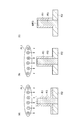
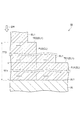
前記第1領域は、それらの高さが互いに異なる複数の凸領域を有し、
被加工物を準備する前記工程は、
前記複数の凸領域の表面上にコンフォーマルに、酸化シリコンから形成された第1の膜を形成する工程と、
前記第1の膜上に酸化シリコンから形成された第2の膜を形成する工程であり、該第2の膜は、その形成位置の高さ方向の位置が高いほど、厚く形成される、該工程と、
前記第1の膜及び前記第2の膜をエッチングする工程であり、前記複数の凸領域のうち一部の凸領域の上端面の上の前記第1の膜及び前記第2の膜が除去され、残された前記第1の膜及び前記第2の膜が前記第2領域を形成する、該工程と、
を含む、方法。 - 前記チャンバ内において前記被加工物は、イオンを該被加工物に引き込むための高周波が供給され得る電極を含むステージ上に搭載され、
第1のガスのプラズマを生成する前記工程において、前記電極に前記高周波が供給される、
請求項1に記載の方法。 - 前記チャンバ内において前記被加工物は、イオンを該被加工物に引き込むための高周波が供給され得る電極を含むステージ上に搭載され、
第2のガスのプラズマを生成する前記工程において、前記電極に前記高周波が供給されない、
請求項1に記載の方法。 - 前記第2のガスは、フッ素を含有する前記ガスとしてNF3ガスを含む、請求項1〜3の何れか一項に記載の方法。
- 前記第2のガスは水素を更に含み、
前記第2のガス中の前記フッ素の原子数に対する前記第2のガス中の前記水素の原子数の比率は、8/9以上である、請求項1〜4の何れか一項に記載の方法。 - 前記第2のガスは、H2ガスを更に含む、請求項4に記載の方法。
- 前記第2のガス中の前記NF3ガスの流量に対する前記第2のガスにおける前記H2ガスの流量の比率は、3/4以上である、請求項6に記載の方法。
- 前記第1のガスは、水素を含有する前記ガスとしてH2ガスを含む、請求項1〜7の何れか一項に記載の方法。
- 第1のガスのプラズマを生成する前記工程及び第2のガスのプラズマを生成する前記工程を各々が含む複数のシーケンスが順に実行される、請求項1〜8の何れか一項に記載の方法。
- 前記被加工物は、シリコンから形成された第3領域を更に含み、
前記第1のガスは、酸素を含有するガスを更に含む、
請求項1〜9の何れか一項に記載の方法。 - 窒化シリコンから形成された第1領域を酸化シリコンから形成された第2領域に対して選択的にエッチングする方法であって、
前記第1領域及び前記第2領域を有する被加工物をプラズマ処理装置のチャンバ本体によって提供されるチャンバ内に準備する工程と、
水素の活性種によって前記第1領域の一部を改質して改質領域を形成するよう、前記チャンバ内で水素を含有するガスを含む第1のガスのプラズマを生成する工程と、
フッ素の活性種によって前記改質領域を除去するよう、前記チャンバ内でフッ素を含有するガスを含む第2のガスのプラズマを生成する工程と、
を含み、
前記被加工物は、シリコンから形成された第3領域を更に含み、
前記第1のガスは、O 2 ガスを更に含む、
方法。 - 前記第1領域は、前記第2領域及び前記第3領域を覆うように設けられている、請求項10に記載の方法。
- 窒化シリコンから形成された第1領域を酸化シリコンから形成された第2領域に対して選択的にエッチングする方法であって、
前記第1領域及び前記第2領域を有する被加工物をプラズマ処理装置のチャンバ本体によって提供されるチャンバ内に準備する工程と、
水素の活性種によって前記第1領域の一部を改質して改質領域を形成するよう、前記チャンバ内で水素を含有するガスを含む第1のガスのプラズマを生成する工程と、
フッ素の活性種によって前記改質領域を除去するよう、前記チャンバ内でフッ素を含有するガスを含む第2のガスのプラズマを生成する工程と、
を含み、
第1のガスのプラズマを生成する前記工程及び第2のガスのプラズマを生成する前記工程を各々が含む複数のシーケンスが順に実行され、
前記被加工物は、シリコンから形成された第3領域を更に有し、
前記複数のシーケンスの実行前に、前記第1領域は前記第2領域及び前記第3領域を覆うように設けられており、
前記複数のシーケンスは、前記第3領域が露出する直前まで、又は、前記第3領域が露出するまで実行される一以上の第1シーケンス、該一以上の第1シーケンスの後に実行される一以上の第2シーケンスであり前記第3領域の表面を酸化させるための該一以上の第2シーケンスを含み、
少なくとも一以上の第2シーケンスにおいて、前記第1のガスは、酸素を含有するガスを更に含む、
方法。 - 前記一以上の第1シーケンスにおいて、前記第1のガスは、酸素を含有する前記ガスを含まない、請求項13に記載の方法。
- 前記複数のシーケンスは、前記一以上の第2シーケンスの後に実行される一以上の第3シーケンスを更に含み、前記一以上の第3シーケンスにおいて、前記第1のガスは、酸素を含有する前記ガスを含まない、請求項13又は14に記載の方法。
- 前記第1のガスにおける水素を含有する前記ガスの流量に対する前記第1のガスにおける酸素を含有する前記ガスの流量の比率は、3/100以上、9/100以下である、請求項10〜15の何れか一項に記載の方法。
- 酸素を含有する前記ガスは、O2ガスである、請求項10及び13〜16の何れか一項に記載の方法。
Priority Applications (7)
| Application Number | Priority Date | Filing Date | Title |
|---|---|---|---|
| KR1020170165222A KR102484252B1 (ko) | 2016-12-13 | 2017-12-04 | 질화 실리콘으로 형성된 제 1 영역을 산화 실리콘으로 형성된 제 2 영역에 대하여 선택적으로 에칭하는 방법 |
| US15/837,195 US10319613B2 (en) | 2016-12-13 | 2017-12-11 | Method of selectively etching first region made of silicon nitride against second region made of silicon oxide |
| CN202111453386.8A CN114156156A (zh) | 2016-12-13 | 2017-12-13 | 蚀刻装置 |
| CN201711326482.XA CN108231579B (zh) | 2016-12-13 | 2017-12-13 | 相对于氧化硅区域有选择地蚀刻氮化硅区域的方法 |
| US16/394,089 US10600660B2 (en) | 2016-12-13 | 2019-04-25 | Method of selectively etching first region made of silicon nitride against second region made of silicon oxide |
| US16/794,391 US11637025B2 (en) | 2016-12-13 | 2020-02-19 | Apparatus for selectively etching first region made of silicon nitride against second region made of silicon oxide |
| KR1020220184475A KR102617192B1 (ko) | 2016-12-13 | 2022-12-26 | 질화 실리콘으로 형성된 제 1 영역을 산화 실리콘으로 형성된 제 2 영역에 대하여 선택적으로 에칭하는 방법 |
Applications Claiming Priority (2)
| Application Number | Priority Date | Filing Date | Title |
|---|---|---|---|
| JP2016240871 | 2016-12-13 | ||
| JP2016240871 | 2016-12-13 |
Publications (2)
| Publication Number | Publication Date |
|---|---|
| JP2018098480A JP2018098480A (ja) | 2018-06-21 |
| JP6836953B2 true JP6836953B2 (ja) | 2021-03-03 |
Family
ID=62633795
Family Applications (1)
| Application Number | Title | Priority Date | Filing Date |
|---|---|---|---|
| JP2017086521A Active JP6836953B2 (ja) | 2016-12-13 | 2017-04-25 | 窒化シリコンから形成された第1領域を酸化シリコンから形成された第2領域に対して選択的にエッチングする方法 |
Country Status (3)
| Country | Link |
|---|---|
| JP (1) | JP6836953B2 (ja) |
| KR (2) | KR102484252B1 (ja) |
| CN (2) | CN108231579B (ja) |
Families Citing this family (4)
| Publication number | Priority date | Publication date | Assignee | Title |
|---|---|---|---|---|
| JP7174634B2 (ja) | 2019-01-18 | 2022-11-17 | 東京エレクトロン株式会社 | 膜をエッチングする方法 |
| JP7333752B2 (ja) | 2019-12-25 | 2023-08-25 | 東京エレクトロン株式会社 | 基板処理方法及び基板処理装置 |
| KR102594634B1 (ko) * | 2020-12-09 | 2023-10-25 | 에스케이스페셜티 주식회사 | 실리콘 함유막의 에칭 방법 및 이를 포함한 반도체 디바이스의 제조방법 |
| US20230386793A1 (en) * | 2021-02-19 | 2023-11-30 | Hitachi High-Tech Corporation | Etching method and etching apparatus |
Family Cites Families (17)
| Publication number | Priority date | Publication date | Assignee | Title |
|---|---|---|---|---|
| US7094670B2 (en) * | 2000-08-11 | 2006-08-22 | Applied Materials, Inc. | Plasma immersion ion implantation process |
| JP4123428B2 (ja) | 2001-11-30 | 2008-07-23 | 東京エレクトロン株式会社 | エッチング方法 |
| TWI462179B (zh) * | 2006-09-28 | 2014-11-21 | Tokyo Electron Ltd | 用以形成氧化矽膜之成膜方法與裝置 |
| US7977249B1 (en) * | 2007-03-07 | 2011-07-12 | Novellus Systems, Inc. | Methods for removing silicon nitride and other materials during fabrication of contacts |
| US8252696B2 (en) * | 2007-10-22 | 2012-08-28 | Applied Materials, Inc. | Selective etching of silicon nitride |
| JP4959733B2 (ja) * | 2008-02-01 | 2012-06-27 | 東京エレクトロン株式会社 | 薄膜形成方法、薄膜形成装置及びプログラム |
| WO2011108663A1 (ja) * | 2010-03-04 | 2011-09-09 | 東京エレクトロン株式会社 | プラズマエッチング方法、半導体デバイスの製造方法、及びプラズマエッチング装置 |
| US8268184B2 (en) * | 2010-06-29 | 2012-09-18 | Tokyo Electron Limited | Etch process for reducing silicon recess |
| US8716154B2 (en) * | 2011-03-04 | 2014-05-06 | Applied Materials, Inc. | Reduced pattern loading using silicon oxide multi-layers |
| JP5712874B2 (ja) * | 2011-09-05 | 2015-05-07 | 東京エレクトロン株式会社 | 成膜装置、成膜方法及び記憶媒体 |
| FR2993576B1 (fr) * | 2012-07-20 | 2018-05-18 | Nanoplas | Dispositif de traitement d'un objet par plasma |
| US8956980B1 (en) * | 2013-09-16 | 2015-02-17 | Applied Materials, Inc. | Selective etch of silicon nitride |
| US8980758B1 (en) * | 2013-09-17 | 2015-03-17 | Applied Materials, Inc. | Methods for etching an etching stop layer utilizing a cyclical etching process |
| JP6230954B2 (ja) | 2014-05-09 | 2017-11-15 | 東京エレクトロン株式会社 | エッチング方法 |
| JP6235981B2 (ja) | 2014-07-01 | 2017-11-22 | 東京エレクトロン株式会社 | 被処理体を処理する方法 |
| JP2016058643A (ja) * | 2014-09-11 | 2016-04-21 | 株式会社Screenホールディングス | プラズマエッチング方法 |
| JP6521848B2 (ja) * | 2015-01-16 | 2019-05-29 | 東京エレクトロン株式会社 | エッチング方法 |
-
2017
- 2017-04-25 JP JP2017086521A patent/JP6836953B2/ja active Active
- 2017-12-04 KR KR1020170165222A patent/KR102484252B1/ko active IP Right Grant
- 2017-12-13 CN CN201711326482.XA patent/CN108231579B/zh active Active
- 2017-12-13 CN CN202111453386.8A patent/CN114156156A/zh active Pending
-
2022
- 2022-12-26 KR KR1020220184475A patent/KR102617192B1/ko active IP Right Grant
Also Published As
| Publication number | Publication date |
|---|---|
| CN108231579A (zh) | 2018-06-29 |
| JP2018098480A (ja) | 2018-06-21 |
| KR102484252B1 (ko) | 2023-01-03 |
| KR20180068290A (ko) | 2018-06-21 |
| CN108231579B (zh) | 2021-12-21 |
| KR20230007289A (ko) | 2023-01-12 |
| CN114156156A (zh) | 2022-03-08 |
| KR102617192B1 (ko) | 2023-12-27 |
Similar Documents
| Publication | Publication Date | Title |
|---|---|---|
| US10600660B2 (en) | Method of selectively etching first region made of silicon nitride against second region made of silicon oxide | |
| JP6235981B2 (ja) | 被処理体を処理する方法 | |
| JP5706946B2 (ja) | プラズマエッチング方法及びプラズマエッチング装置 | |
| KR102617192B1 (ko) | 질화 실리콘으로 형성된 제 1 영역을 산화 실리콘으로 형성된 제 2 영역에 대하여 선택적으로 에칭하는 방법 | |
| TWI627724B (zh) | 在先進圖案化製程中用於間隔物沉積與選擇性移除的設備與方法 | |
| TWI657499B (zh) | 蝕刻方法 | |
| TWI818033B (zh) | 用來釋放薄膜的應力的原位高功率植入 | |
| US11462412B2 (en) | Etching method | |
| TWI722187B (zh) | 蝕刻方法 | |
| US10755944B2 (en) | Etching method and plasma processing apparatus | |
| TW202002014A (zh) | 基板處理方法及基板處理裝置 | |
| US20220246440A1 (en) | Substrate processing method and substrate processing apparatus | |
| JP7296602B2 (ja) | SiC基板の製造方法 | |
| CN114188218A (zh) | 蚀刻处理方法以及基板处理装置 |
Legal Events
| Date | Code | Title | Description |
|---|---|---|---|
| A621 | Written request for application examination |
Free format text: JAPANESE INTERMEDIATE CODE: A621 Effective date: 20191225 |
|
| A977 | Report on retrieval |
Free format text: JAPANESE INTERMEDIATE CODE: A971007 Effective date: 20201019 |
|
| A131 | Notification of reasons for refusal |
Free format text: JAPANESE INTERMEDIATE CODE: A131 Effective date: 20201027 |
|
| A521 | Request for written amendment filed |
Free format text: JAPANESE INTERMEDIATE CODE: A523 Effective date: 20201208 |
|
| TRDD | Decision of grant or rejection written | ||
| A01 | Written decision to grant a patent or to grant a registration (utility model) |
Free format text: JAPANESE INTERMEDIATE CODE: A01 Effective date: 20210112 |
|
| A61 | First payment of annual fees (during grant procedure) |
Free format text: JAPANESE INTERMEDIATE CODE: A61 Effective date: 20210208 |
|
| R150 | Certificate of patent or registration of utility model |
Ref document number: 6836953 Country of ref document: JP Free format text: JAPANESE INTERMEDIATE CODE: R150 |
|
| R250 | Receipt of annual fees |
Free format text: JAPANESE INTERMEDIATE CODE: R250 |